WO2010137164A1 - キャッシュ制御装置およびキャッシュ制御方法 - Google Patents
キャッシュ制御装置およびキャッシュ制御方法 Download PDFInfo
- Publication number
- WO2010137164A1 WO2010137164A1 PCT/JP2009/059871 JP2009059871W WO2010137164A1 WO 2010137164 A1 WO2010137164 A1 WO 2010137164A1 JP 2009059871 W JP2009059871 W JP 2009059871W WO 2010137164 A1 WO2010137164 A1 WO 2010137164A1
- Authority
- WO
- WIPO (PCT)
- Prior art keywords
- cache
- power consumption
- predetermined threshold
- operation rate
- data
- Prior art date
- Legal status (The legal status is an assumption and is not a legal conclusion. Google has not performed a legal analysis and makes no representation as to the accuracy of the status listed.)
- Ceased
Links
Images

Classifications
-
- G—PHYSICS
- G06—COMPUTING OR CALCULATING; COUNTING
- G06F—ELECTRIC DIGITAL DATA PROCESSING
- G06F12/00—Accessing, addressing or allocating within memory systems or architectures
- G06F12/02—Addressing or allocation; Relocation
- G06F12/08—Addressing or allocation; Relocation in hierarchically structured memory systems, e.g. virtual memory systems
- G06F12/0802—Addressing of a memory level in which the access to the desired data or data block requires associative addressing means, e.g. caches
- G06F12/0891—Addressing of a memory level in which the access to the desired data or data block requires associative addressing means, e.g. caches using clearing, invalidating or resetting means
-
- G—PHYSICS
- G06—COMPUTING OR CALCULATING; COUNTING
- G06F—ELECTRIC DIGITAL DATA PROCESSING
- G06F2212/00—Indexing scheme relating to accessing, addressing or allocation within memory systems or architectures
- G06F2212/10—Providing a specific technical effect
- G06F2212/1028—Power efficiency
-
- G—PHYSICS
- G06—COMPUTING OR CALCULATING; COUNTING
- G06F—ELECTRIC DIGITAL DATA PROCESSING
- G06F2212/00—Indexing scheme relating to accessing, addressing or allocation within memory systems or architectures
- G06F2212/50—Control mechanisms for virtual memory, cache or TLB
- G06F2212/502—Control mechanisms for virtual memory, cache or TLB using adaptive policy
-
- G—PHYSICS
- G06—COMPUTING OR CALCULATING; COUNTING
- G06F—ELECTRIC DIGITAL DATA PROCESSING
- G06F2212/00—Indexing scheme relating to accessing, addressing or allocation within memory systems or architectures
- G06F2212/60—Details of cache memory
- G06F2212/603—Details of cache memory of operating mode, e.g. cache mode or local memory mode
-
- Y—GENERAL TAGGING OF NEW TECHNOLOGICAL DEVELOPMENTS; GENERAL TAGGING OF CROSS-SECTIONAL TECHNOLOGIES SPANNING OVER SEVERAL SECTIONS OF THE IPC; TECHNICAL SUBJECTS COVERED BY FORMER USPC CROSS-REFERENCE ART COLLECTIONS [XRACs] AND DIGESTS
- Y02—TECHNOLOGIES OR APPLICATIONS FOR MITIGATION OR ADAPTATION AGAINST CLIMATE CHANGE
- Y02D—CLIMATE CHANGE MITIGATION TECHNOLOGIES IN INFORMATION AND COMMUNICATION TECHNOLOGIES [ICT], I.E. INFORMATION AND COMMUNICATION TECHNOLOGIES AIMING AT THE REDUCTION OF THEIR OWN ENERGY USE
- Y02D10/00—Energy efficient computing, e.g. low power processors, power management or thermal management
Definitions
- the present invention relates to a cache control device and a cache control method for controlling a cache memory.
- the cache control circuit is provided with an external circuit for controlling the operation clock or an external circuit for performing voltage fluctuation control, and these external circuits vary the operation clock and voltage.
- Patent Documents 10 to 12 a technique for temporarily disconnecting a cache memory when power consumption is high is known (for example, Patent Documents 10 to 12). Specifically, when it is determined that the power consumption is high, after the dirty data that is not stored in the main storage device and exists only in the cache memory is written from the cache memory to the main storage device, Performs processing to separate cache memory.
- JP-A-8-45275 JP-A-2-040194 Japanese Patent Laid-Open No. 9-274796 Japanese Patent Laid-Open No. 2-310762 JP 2008-146812 A JP-A-8-8991 JP-A-11-177737 JP-A-5-94227 JP 2004-303206 A JP 2001-109729 A Special table 2003-530640 gazette Japanese Patent Laid-Open No. 2-151950
- the dirty data stored in the cache memory is written to the main storage device. Therefore, the processing load for writing the dirty data to the main storage device may increase, and the separation process is performed. As a result, it took time, and there was a problem that power consumption could not be reduced immediately.
- the disclosed technology has been made in view of the above, and aims to reduce power consumption immediately without increasing the circuit scale.
- the cache control device disclosed in the present application is, when it is determined that the power consumption is equal to or higher than a predetermined threshold, or when the cache memory operation rate is determined to be equal to or lower than the predetermined threshold,
- the cache memory is controlled to degenerate the same information storage area that stores only the same information as the information stored on the main storage device.
- the cache control device disclosed in the present application it is possible to immediately reduce power consumption without increasing the circuit scale.
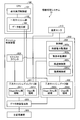
- FIG. 1 is a block diagram illustrating the configuration of the information processing apparatus according to the first embodiment.
- FIG. 2 is a diagram for explaining the data structure of the secondary cache directory unit.
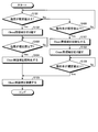
- FIG. 3 is a flowchart illustrating the flow of the disconnection process and the return process of the cache control device according to the first embodiment.
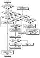
- FIG. 4 is a flowchart illustrating the flow of the cache registration process of the cache control device according to the first embodiment.
- FIG. 1 is a block diagram illustrating the configuration of the cache control apparatus 200 according to the first embodiment.
- the information processing system 10 includes a CPU 100, a temperature sensor 110, a cache control device 200, and a main storage device 300, which are connected to each other via a bus or the like. The processing of each of these units will be described below.
- the CPU 100 is a processor core block and includes an instruction execution control unit 101 and a primary cache unit 102.
- the instruction execution control unit 101 retrieves an instruction from the main storage device 300 via the primary cache, and executes and executes the instruction.
- the primary cache unit 102 has a data restoration unit 103, receives a request from the instruction execution unit 101, and accesses data to the primary cache. Further, the primary cache unit 102 accesses the secondary cache when data is not registered in the primary cache.
- the temperature sensor 110 measures the temperature of its own device and notifies the control unit 205 of the cache control device 200 of the temperature information.
- the data restoration unit 103 restores the data received from the cache control device 200. Specifically, when receiving data and a data inversion flag from the cache control device 200, the data restoration unit 103 determines whether to invert data using the inversion flag. That is, when the data inversion flag is “1”, the data restoration unit 103 restores the data by inverting the data.
- the cache control device 200 receives a request from the primary cache unit 102 and accesses data to the secondary cache. When the cache control device 200 is not registered in the secondary cache, the cache control device 200 accesses the main storage device 300. If it is registered in the secondary cache, it reads out from the data part and responds to the primary cache part 102.
- the cache control device 200 includes a secondary cache directory unit 201, a secondary cache data unit 202, a data inspection / restoration unit 203, a request counter 204, and a control unit 205. The processing of each of these units will be described below.
- the secondary cache directory unit 201 records status information related to the status of data registered in the secondary cache data unit 202.
- the secondary cache directory unit 201 includes a Clean / Dirty area 2011 for storing state information regarding Clean registration data and a state information regarding Dirty registration data, and a Clean area storing only state information regarding Clean registration data. 2012.
- FIG. 2 is a diagram for explaining the data structure of the secondary cache directory unit. Specifically, as shown in FIG. 2, the secondary cache directory unit 201 displays a “physical address” indicating the address of the registered data, a “status” indicating the status of the registered data in the secondary cache, and the status of the registered data. “Inversion flag” indicating “first cache status” indicating the state of registered data in the primary cache is stored.
- the “inversion flag” indicating the status of the registration data is “0”, it indicates that the registration data is registered as it is, and when the “inversion flag” is “1”, Indicates that registration data is reversed and registered.
- the registration data in the primary cache indicates that the registration data is invalid, and “10: clean”. Indicates that the registration data matches the data in the main storage device 300. If “11: exclusive”, the registration data may not match the data in the main storage device 300. Show.
- the secondary cache data section 202 stores the recorded data body.
- the secondary cache data unit 202 includes a Clean / Dirty area 2021 for storing Clean registration data and Dirty registration data, and a Clean area 2022 for storing only Clean registration data.
- the secondary cache data unit 202 is roughly divided into a Clean / Dirty area 2021 and a Clean area 2022.
- the area may be divided in the way direction, for example.
- the dirty data is data updated by the CPU 100 and means data that is not stored in the main storage device 300 and exists only in the cache memory.
- the clean data refers to the same data as the data stored on the main storage device 300.
- the secondary cache data unit 202 registers the data in the Clean / Dirty area 2021 because the data may become Dirty. If the request from the CPU 100 is a read command, the data is Clean, and therefore, the request is registered in the Clean area 2022 or the Clean / Dirty area 2021.
- the data inspection / restoration unit 203 counts the number of “1” s in the data, and sends the inverted data to the secondary cache data unit 202 if the number is greater than half the data length. If not, send the data as it is. In addition, when the data is inverted, the data inspection / restoration unit 203 notifies the secondary cache directory unit 201 that the data has been inverted. In the case of a write back, the reverse flag is received from the secondary cache directory unit 201 and the restored data is sent to the main storage device 300.
- the request counter 204 measures the number of requests to the secondary cache within a predetermined time and notifies the control unit 205 of it.
- the control unit 205 performs degeneration control processing and recovery control processing on the secondary cache data unit 202, and in particular includes a power consumption monitoring unit 205a, an operation rate monitoring unit 205b, a degeneration control unit 205c, and a recovery control unit 205d. .
- the power consumption monitoring unit 205a monitors information related to the power consumption of the own device, and determines whether the information related to power consumption is equal to or greater than a predetermined threshold. Specifically, the power consumption monitoring unit 205a receives temperature information from the temperature sensor 110 as information regarding power consumption, and determines whether the temperature of the own device is equal to or higher than a predetermined threshold. As a result, when the temperature of the own device is equal to or higher than a predetermined threshold, the power consumption monitoring unit 205a notifies the degeneration control unit 205c to that effect.
- the power consumption monitoring unit 205a receives temperature information from the temperature sensor 110 and determines whether the temperature of the own device is equal to or lower than a predetermined threshold. As a result, the power consumption monitoring unit 205a notifies the return control unit 205d of the fact that the temperature of the device itself is equal to or lower than a predetermined threshold value.
- the operation rate monitoring unit 205b monitors the operation rate of the secondary cache memory and determines whether the secondary cache memory operation rate is equal to or less than a predetermined threshold. Specifically, the operation rate monitoring unit 205b receives the number of requests to the secondary cache within a predetermined time from the request counter 204 as the operation rate of the secondary cache memory, and the number of requests is equal to or less than a predetermined threshold. Determine whether. As a result, when the number of requests is equal to or less than a predetermined threshold, the operation rate monitoring unit 205b notifies the degeneration control unit 205c to that effect.
- the operation rate monitoring unit 205b receives the number of requests to the secondary cache within a predetermined time from the request counter 204, and the number of requests is a predetermined threshold value. It is determined whether it is above. As a result, when the number of requests is equal to or greater than a predetermined threshold, the power consumption monitoring unit 205a notifies the return control unit 205d to that effect.
- the degeneration control unit 205c uses the Clean for the secondary cache data unit 202. Control is performed so that the area 2022 is degenerated. Specifically, when the degeneration control unit 205c receives a notification from the power consumption monitoring unit 205a that the temperature of its own device is equal to or higher than a predetermined threshold, the degeneration control unit 205c promptly uses the Clean area of the secondary cache data unit 202. Disconnecting 2022 is performed.
- the degeneration control unit 205c when the degeneration control unit 205c receives a notification from the operation rate monitoring unit 205b that the number of requests is equal to or less than a predetermined threshold, the degeneration control unit 205c initializes the Clean area 2012 of the secondary cache directory unit 201, After the initialization is completed, the Clean area 2022 of the secondary cache data unit 202 is disconnected.
- the power consumed by the separated Clean area 2022 is reduced. Further, since the Clean area 2022 is disconnected and the number of cache misses increases, the number of accesses to the main storage device 300 increases. As a result, the operating rate of the CPU 100 decreases, and the operating power of the CPU 100 is also reduced.
- the Clean data exists on the main storage device 300, even if the Clean area 2022 in which the Clean data is registered is disconnected, the data can be acquired by accessing the main storage device 300 again. . Therefore, in this disconnection operation, it is not necessary to write out dirty data to the main storage device, so that the degeneration control process can be executed immediately.
- a method for separating the Clean area 2022 of the secondary cache data unit 202 As a method for separating the Clean area 2022 of the secondary cache data unit 202, a method of suppressing access, a method of suppressing application of a clock, a method of stopping power supply using a power gate, and the like can be considered. Any method may be used as long as power consumption is reduced.
- the return control unit 205d uses the Clean for the secondary cache data unit 202. Control is performed so that the area 2022 is restored.
- the recovery control unit 205d determines that the temperature state has recovered when receiving a notification from the power consumption monitoring unit 205a that the temperature of its own device is equal to or lower than a predetermined threshold,
- the Clean area 2012 of the cache directory unit 201 is initialized, and after the initialization is completed, the Clean area 2022 of the secondary cache data unit 202 is reconnected.
- the restoration control unit 205d promptly reconnects the Clean area 2022 of the secondary cache data unit 202. Do.
- the cache control device 200 is in a state where the power consumption is over when the temperature of the device itself is equal to or higher than a predetermined threshold, and the immediacy of power saving is required.
- the Clean area 2022 is immediately separated without initializing the Clean area 2012 of the unit 201. Thereafter, the cache control device 200 cancels the state where the power consumption has exceeded, and immediately before the re-connection of the Clean area 2022 of the secondary cache data section 202, the initial state of the Clean area 2012 of the secondary cache directory section 201 is established. To do.
- the cache control device 200 when the number of requests to the secondary cache is equal to or less than the predetermined threshold, the cache control device 200 is not in a state where the power consumption is over, but is required to have immediate power saving. Therefore, after the Clean area 2012 of the secondary cache directory unit 201 is initialized, the Clean area 2022 is disconnected. Thereafter, when the number of requests to the secondary cache exceeds a predetermined threshold, the cache control apparatus 200 wants to immediately return the Clean area 2022, so the Clean area 2022 of the secondary cache data unit 202 is used. Reconnect quickly.
- the main storage device 300 includes a main memory of the information processing device, and stores all instructions and data necessary for arithmetic processing by the CPU 100. Of these instructions and data, frequently used ones are stored in the secondary cache data unit 202 or the primary cache unit 102 in the CPU 100.
- FIG. 3 is a flowchart illustrating the flow of the disconnection process and the return process of the cache control device according to the first embodiment.
- FIG. 4 is a flowchart illustrating the flow of the cache registration process of the cache control device according to the first embodiment.
- the power consumption monitoring unit 205 a of the cache control device 200 receives temperature information from the temperature sensor 110 as information regarding power consumption, and determines whether the temperature of the own device is equal to or higher than a predetermined threshold. (Step S101). As a result, when it is determined that the temperature of the own device is equal to or higher than the predetermined threshold value (Yes in step S101), the degeneration control unit 205c quickly separates the Clean area 2022 of the secondary cache data unit 202. (Step S102).
- the power consumption monitoring unit 205a receives the temperature information from the temperature sensor 110 and determines whether the temperature of the own apparatus is equal to or lower than a predetermined threshold ( Step S103).
- Step S104 the return control unit 205d initializes the Clean area 2012 of the secondary cache directory unit 201 ( Step S104) After the initialization is completed, reconnection of the Clean area 2022 of the secondary cache data unit 202 is performed (Step S105).
- the operation rate monitoring unit 205b has the number of requests as the operation rate of the secondary cache memory equal to or less than the predetermined threshold. Is determined (step S106). As a result, when it is determined that the number of requests is not equal to or less than the predetermined threshold (No at Step S106), the process returns to S101.
- the degeneration control unit 205c initializes the Clean area 2012 of the secondary cache directory unit 201 (Step S107). After the initialization is completed, the Clean area 2022 of the secondary cache data unit 202 is disconnected (step S108).
- the operation rate monitoring unit 205b receives the number of requests to the secondary cache within a predetermined time from the request counter 204, and the number of requests is a predetermined threshold value. It is determined whether this is the case (step S109). As a result, when it is determined that the number of requests is not equal to or greater than the predetermined threshold (No at Step S109), the process returns to S109.
- Step S109 If it is determined that the number of requests is equal to or greater than the predetermined threshold (Yes at Step S109), the return control unit 205d promptly reconnects the Clean area 2022 of the secondary cache data unit 202 (Step S109). S105).
- the cache control device 200 determines whether the request from the CPU 100 is a store instruction and hits the Clean area 2022 of the secondary cache data unit 202 (step S301).
- Step S301 if it is determined that the cache control device 200 is not a store instruction or has not hit the Clean area 2022 (No at Step S301), the cache control device 200 determines whether the secondary cache data unit 202 has been hit (No). Step S302).
- the cache control device 200 determines whether the replacement data of the primary cache is Dirty data (Step S303).
- the cache control device 200 writes back to the secondary cache according to the inversion flag (Step S304). Then, the cache control device 200 reads the requested data from the secondary cache data unit 202 and transfers it to the CPU 100 together with the data inversion flag (step S315).
- the cache control device 200 reads the requested data from the secondary cache data unit 202 without writing back to the secondary cache. Then, the data is transferred together with the data inversion flag to the CPU 100 (step S315).
- the cache controller 200 determines whether the request is a read command (step S302). S305). As a result, when the request is a read command (Yes at Step S305), the cache control device 200 determines whether or not there is a vacancy in the Clean area 2022 (Step S306). As a result, when the Clean area 2022 is free (Yes at Step S306), the cache control device 200 uses the free entry (Step S309).
- the cache control apparatus 200 determines whether there is a space in the Clean / Dirty area 2021 (Step S307). As a result, when the Clean / Dirty area 2021 has a free space (Yes at Step S307), the cache control device 200 uses the free entry (Step S309).
- the cache control apparatus 200 determines the replacement target as the Clean area 2022, and the entry that is least used in the Clean area 2022 is used. Is deleted to create a space (step S308).
- the cache control device 200 reads the main storage device 300 data (step S310), and determines whether “1” is more in the read data (step S311). If there is more “1” in the read data (Yes at Step S311), the cache control device 200 inverts the data (Step S312). Further, when “1” is less in the read data (No at Step S311), the cache control device 200 does not invert the data (Step S313).
- the cache control device 200 registers the data in the secondary cache data unit 202 (step S314), reads the requested data from the secondary cache data unit 202 without writing back to the secondary cache, and inverts the data. It transfers to CPU100 with a flag (step S315).
- step S301 when the cache control device 200 determines in S301 that the request from the CPU 100 is a store instruction and hits the Clean area 2022 of the secondary cache data unit 202 (Yes in step S301), The hit entry in the Clean area 2022 is deleted (step S316).
- the cache control device 200 determines whether or not there is a free space in the Clean / Dirty area 2022 (Step S317). As a result, when the Clean / Dirty area 2022 is empty (Yes at Step S317), the cache control apparatus 200 proceeds to Step S309 described above.
- the cache control apparatus 200 determines whether the data of the least used entry in the Clean / Dirty area 2021 is Clean data. Determination is made (step S318).
- Step S318 when the data of the least used entry in the Clean / Dirty area 2021 is Clean data (Yes in Step S318), the cache control apparatus 200 sets the replacement target in the Clean / Dirty area 2021. decide. Then, the cache control device 200 deletes the entry of the Clean data in the Clean / Dirty area 2021 to create a space (Step S319), and proceeds to Step S310 described above.
- the cache control apparatus 200 determines the replacement target as the Clean / Dirty area 2021. . Then, the cache control device 200 transfers the Dirtyna data together with the inversion information to the data restoration unit 103, writes the data restored by the CPU 100 in accordance with the inversion information to the main storage device 300 to create a space (step S320), and the steps described above. The process proceeds to S310.
- the cache control device 200 has the Clean area 2022 in the secondary cache data unit 202 that stores only the same information as the information stored in the main storage device 300. Then, the cache control device 200 monitors information related to the power consumption of the own device, determines whether the information related to power consumption is equal to or greater than a predetermined threshold, monitors the operation rate of the secondary cache memory, and the operation rate is predetermined. It is judged whether it is below the threshold value.
- the cache control device 200 Control is performed so that the Clean area 2022 on the secondary cache data section 202 is degenerated. For this reason, the cache control apparatus 200 does not need to write out dirty data to the main storage device 300 in the degeneration control of the Clean area 2022, and therefore can execute the degeneration control process immediately. As a result, the cache control device 200 has an effect that power consumption can be immediately reduced without increasing the circuit scale.
- the cache control device 200 indicates the state of data stored in the Clean area 2022 when it is determined that the operation rate of the secondary cache memory is equal to or less than a predetermined threshold.
- the cache directory is initialized, and control is performed so that the Clean area 2022 is degenerated. Therefore, the cache control device 200 can quickly reconnect the Clean area 2022 of the secondary cache data unit 202 when the cache usage frequency becomes high.
- the cache control apparatus 200 monitors the information regarding power consumption after the Clean area 2022 is degenerated, and the information regarding power consumption is equal to or less than a predetermined threshold. Determine whether.
- the cache control apparatus 200 monitors the operation rate of the secondary cache memory after the control is performed so that the Clean area 2022 is degenerated, and determines whether the operation rate is equal to or higher than a predetermined threshold.
- the cache control device 200 determines that the information regarding the power consumption is equal to or lower than the predetermined threshold value, or when the operation rate of the secondary cache memory is determined to be equal to or higher than the predetermined threshold value, the cache control device 200 Control is performed so that the work area 2022 returns. For this reason, the cache control device 200 can immediately execute the restoration process of the Clean area 2022 when the power consumption over is resolved or the use frequency of the cache becomes high.
- the cache control device 200 initializes the cache directory stored in the Clean area 2012 when it is determined that the information regarding the power consumption is equal to or less than the predetermined threshold. Control is performed so that the Clean area 2022 of the secondary cache data unit 202 is restored. For this reason, the cache control device 200 initializes the Clean area 2012 of the secondary cache directory unit 201 immediately before reconnecting the Clean area 2022, and performs the degeneration control, the secondary cache directory Since the Clean area 2012 of the unit 201 is not initialized, the Clean area 2022 can be quickly separated.
- the cache control device 200 monitors the temperature of its own device as information regarding the power consumption of its own device, and determines whether the temperature is equal to or higher than a predetermined threshold. It is possible to determine whether or not the power consumption of the own device is high.
- the cache control device 200 monitors the number of requests to the secondary cache data unit 202 in a predetermined time as the operation rate of the cache memory, and the number of requests in the predetermined time is equal to or less than a predetermined threshold value. Therefore, it is possible to determine whether or not the operation rate of the cache memory is high by using the number of requests within a predetermined time.
- each component of each illustrated apparatus is functionally conceptual and does not necessarily need to be physically configured as illustrated.
- the specific form of distribution / integration of each device is not limited to that shown in the figure, and all or a part thereof may be functionally or physically distributed or arbitrarily distributed in arbitrary units according to various loads or usage conditions. Can be integrated and configured.
- the degeneration control unit 205c and the return control unit 205d may be integrated.
- all or any part of each processing function performed in each device may be realized by a CPU and a program analyzed and executed by the CPU, or may be realized as hardware by wired logic.
- the cache control method described in the present embodiment can be realized by executing a prepared program on a computer such as a personal computer or a workstation.
- This program can be distributed via a network such as the Internet.
- the program can also be executed by being recorded on a computer-readable recording medium such as a hard disk, a flexible disk (FD), a CD-ROM, an MO, and a DVD and being read from the recording medium by the computer.
- a computer-readable recording medium such as a hard disk, a flexible disk (FD), a CD-ROM, an MO, and a DVD and being read from the recording medium by the computer.
Landscapes
- Engineering & Computer Science (AREA)
- Theoretical Computer Science (AREA)
- Physics & Mathematics (AREA)
- General Engineering & Computer Science (AREA)
- General Physics & Mathematics (AREA)
- Memory System Of A Hierarchy Structure (AREA)
Abstract
キャッシュ制御装置(200)は、主記憶装置(300)上に格納されている情報と同一の情報のみを記憶するClean用領域(2022)を二次キャッシュデータ部(202)上に有する。そして、キャッシュ制御装置(200)は、自装置の消費電力に関する情報を監視し、消費電力に関する情報が所定の閾値以上であるかを判定し、また、キャッシュメモリの動作率を監視し、動作率が所定の閾値以下であるかを判定する。続いて、キャッシュ制御装置(200)は、消費電力に関する情報が所定の閾値以上であると判定された場合、または、二次キャッシュメモリの動作率が所定の閾値以下であると判定された場合には、二次キャッシュデータ部(202)上のClean用領域(2022)を縮退するように制御する。
Description
この発明は、キャッシュメモリを制御するキャッシュ制御装置およびキャッシュ制御方法に関する。
従来より、処理速度を上げるために、主記憶装置ではなくアクセス速度の速いキャッシュメモリにデータを確保するキャッシュ制御回路が知られている。近年、このようなキャッシュ制御回路において、半導体製造技術が向上し微細化が進むにつれ、集積度や漏れ電流の増大により消費電力が大きく、省電力化が注目されている(例えば、特許文献1~7参照)。
例えば、省電力を目的とした技術として、動作クロックや電圧を変動するように制御する技術が知られている(例えば、特許文献8、9参照)。具体的には、キャッシュ制御回路に動作クロックの制御を行う外部回路または電圧の変動制御を行うための外部回路が設けられ、これらの外部回路が動作クロックや電圧を変動させる。
また、省電力化を目的とした技術として、消費電力が高い場合に、キャッシュメモリを一時的に切り離す技術が知られている(例えば、特許文献10~12)。具体的には、消費電力が高いと判定された場合に、主記憶装置上に格納されておらずキャッシュメモリにのみ存在するデータであるDirtyなデータをキャッシュメモリから主記憶装置へ書き出した後に、キャッシュメモリを切り離す処理を行う。
しかしながら、上記の動作クロックや電圧を変動する技術では、動作クロックの制御を行う外部回路または電圧の変動制御を行うための複雑な外部回路が必要であり、回路規模が大きくなり、製造コストが大きくなるという課題があった。
また、上記のキャッシュメモリを切り離す技術では、キャッシュメモリに格納されたDirtyなデータを主記憶装置へ書き出すので、Dirtyなデータを主記憶装置へ書き出す処理負荷が高くなる場合があり、切り離し処理を行うまでに時間が掛かる結果、即時に消費電力の削減を行えないという課題があった。
開示の技術は、上記に鑑みてなされたものであって、回路規模を大きくすることなく、消費電力の即時削減を行うことを目的とする。
本願の開示するキャッシュ制御装置は、一つの態様において、消費電力が所定の閾値以上であると判定された場合、または、キャッシュメモリ動作率が所定の閾値以下であると判定された場合には、主記憶装置上に格納されている情報と同一の情報のみを記憶する同一情報記憶領域を縮退するようにキャッシュメモリを制御する。
本願の開示するキャッシュ制御装置の一つの態様によれば、回路規模を大きくすることなく、消費電力の即時削減を行うことができるという効果を奏する。
以下に添付図面を参照して、この発明に係るキャッシュ制御装置およびキャッシュ制御方法の実施例を詳細に説明する。
以下の実施例では、実施例1に係るキャッシュ制御装置の構成および処理の流れを順に説明し、最後に実施例1による効果を説明する。
[キャッシュ制御装置の構成]
まず最初に、図1を用いて、実施例1に係るキャッシュ制御装置200を含む情報処理システム10の構成を説明する。図1は、実施例1に係るキャッシュ制御装置200の構成を示すブロック図である。
まず最初に、図1を用いて、実施例1に係るキャッシュ制御装置200を含む情報処理システム10の構成を説明する。図1は、実施例1に係るキャッシュ制御装置200の構成を示すブロック図である。
図1に示すように、この情報処理システム10は、CPU100、温度センサ110、キャッシュ制御装置200、主記憶装置300を有し、バス等を介してそれぞれ接続されている。以下にこれらの各部の処理を説明する。
CPU100は、プロセッサコアブロックであって、命令実行制御部101および1次キャッシュ部102を有する。命令実行制御部101は、一次キャッシュ経由で主記憶装置300から命令を取り出し、命令の実行・演算を行なう。
1次キャッシュ部102は、データ復元部103を有し、命令実行部101からのリクエストを受け、データのアクセスを一次キャッシュに対して行なう。また、1次キャッシュ部102は、一次キャッシュにデータが登録されていなかった場合には、二次キャッシュをアクセスする。温度センサ110は、自装置の温度を測定し、温度情報をキャッシュ制御装置200の制御部205に通知する。
データ復元部103は、キャッシュ制御装置200から受信したデータを復元する。具体的には、データ復元部103は、キャッシュ制御装置200からデータとデータ反転フラグとを受信すると、反転フラグを用いてデータを反転させるか否かを判断する。つまり、データ復元部103は、データ反転フラグが「1」である場合には、データを反転させてデータを復元する。
キャッシュ制御装置200は、一次キャッシュ部102からのリクエストを受け、データのアクセスを二次キャッシュに対して行なう。そして、キャッシュ制御装置200は、二次キャッシュに登録されていなかった場合は、主記憶装置300をアクセスする。また、二次キャッシュに登録されていた場合、データ部から読み出して一次キャッシュ部102へ応答する。
また、キャッシュ制御装置200は、二次キャッシュディレクトリ部201、二次キャッシュデータ部202、データ検査復元部203、リクエストカウンタ204、制御部205を有する。以下にこれらの各部の処理を説明する。
二次キャッシュディレクトリ部201は、二次キャッシュデータ部202に登録されたデータの状態に関する状態情報を記録する。また、二次キャッシュディレクトリ部201は、Cleanな登録データに関する状態情報およびDirtyな登録データに関する状態情報を記憶するClean/Dirty用領域2011と、Cleanな登録データに関する状態情報のみを記憶するClean用領域2012とを有する。
ここで二次キャッシュディレクトリ部201が記憶する状態情報について具体的に説明する。図2は、二次キャッシュディレクトリ部のデータ構成について説明するための図である。具体的には、二次キャッシュディレクトリ部201は、図2に示すように、登録データのアドレスを示す「物理アドレス」、二次キャッシュにおける登録データの状態を示す「ステータス」、登録データの状態を示す「反転フラグ」、一次キャッシュにおける登録データの状態を示す「一次キャッシュステータス」を記憶する。
例えば、二次キャッシュにおける登録データの状態を示す「ステータス」において、「00:invalid」である場合には、登録データが無効であることを示し、「10:clean」である場合には、登録データが主記憶装置300のデータと一致していることを示し、「11:dirty」である場合には、登録データが主記憶装置300のデータと一致していないことを示す。
また、例えば、登録データの状態を示す「反転フラグ」が「0」である場合には、登録データがそのまま登録されていることを示し、「反転フラグ」が「1」である場合には、登録データが反転して登録されていることを示す。
また、例えば、一次キャッシュにおける登録データの状態を示す「一次キャッシュステータス」において、「00:invalid」である場合には、登録データが無効であることを示し、「10:clean」である場合には、登録データが主記憶装置300のデータと一致していることを示し、「11:exclusive」である場合には、登録データが主記憶装置300のデータと一致していない場合があることを示す。
二次キャッシュデータ部202は、記録されたデータ本体が格納されている。また、二次キャッシュデータ部202は、Cleanな登録データおよびDirtyな登録データを記憶するClean/Dirty用領域2021と、Cleanな登録データのみを記憶するClean用領域2022とを有する。
つまり、二次キャッシュデータ部202は、Clean/Dirty用領域2021とClean用領域2022とで大きく二つに分けられている。なお、領域の分割は、例えばWay方向で行なってもよい。ここで、Dirtyなデータとは、CPU100により更新されたデータであり、主記憶装置300上に格納されておらずキャッシュメモリにのみ存在するデータのことをいう。一方、Cleanなデータとは、主記憶装置300上に格納されているデータと同一のデータのことをいう。
ここで、Clean/Dirty用領域2021またはClean用領域2022のデータの登録先を分ける処理について説明する。なお、詳細な処理の流れについては、後に図5を用いて詳述する。二次キャッシュデータ部202は、CPU100からのリクエストがstore命令である場合には、そのデータがDirtyとなる可能性があるため、Clean/Dirty用領域2021へ登録する。また、CPU100からのリクエストがread命令である場合には、そのデータがCleanであるため、Clean用領域2022またはClean/Dirty用領域2021へ登録する。
データ検査復元部203は、データ中の「1」の数を数え、データ長の半分よりも多い場合、反転したデータを二次キャッシュデータ部202へ送る。そうでなかった場合には、そのままのデータを送る。また、データ検査復元部203は、データが反転した場合は、さらに二次キャッシュディレクトリ部201へ反転したことを通知する。またwrite backの際は、二次キャッシュディレクトリ部201から反転フラグを受け取り、復元したデータを主記憶装置300へと送る。
リクエストカウンタ204は、所定の時間内における二次キャッシュへのリクエスト数を測定し、制御部205に通知する。制御部205は、二次キャッシュデータ部202に対して縮退制御処理および復帰制御処理を行うが、特に、消費電力監視部205a、動作率監視部205b、縮退制御部205c、復帰制御部205dを有する。
消費電力監視部205aは、自装置の消費電力に関する情報を監視し、消費電力に関する情報が所定の閾値以上であるかを判定する。具体的には、消費電力監視部205aは、消費電力に関する情報として、温度センサ110から温度情報を受信し、自装置の温度が所定の閾値以上であるかを判定する。この結果、消費電力監視部205aは、自装置の温度が所定の閾値以上である場合には、その旨を縮退制御部205cに通知する。
また、消費電力監視部205aは、縮退制御部205cによって縮退制御が行われた後においては、温度センサ110から温度情報を受信し、自装置の温度が所定の閾値以下であるかを判定する。この結果、消費電力監視部205aは、自装置の温度が所定の閾値以下である場合には、その旨を復帰制御部205dに通知する。
動作率監視部205bは、二次キャッシュメモリの動作率を監視し、二次キャッシュメモリ動作率が所定の閾値以下であるかを判定する。具体的には、動作率監視部205bは、二次キャッシュメモリの動作率として、リクエストカウンタ204から所定の時間内における二次キャッシュへのリクエスト数を受信し、リクエスト数が所定の閾値以下であるかを判定する。この結果、動作率監視部205bは、リクエスト数が所定の閾値以下である場合には、その旨を縮退制御部205cに通知する。
また、動作率監視部205bは、縮退制御部205cによって縮退制御が行われた後においては、リクエストカウンタ204から所定の時間内における二次キャッシュへのリクエスト数を受信し、リクエスト数が所定の閾値以上であるかを判定する。この結果、消費電力監視部205aは、リクエスト数が所定の閾値以上である場合には、その旨を復帰制御部205dに通知する。
縮退制御部205cは、消費電力に関する情報が所定の閾値以上であると判定された場合、または動作率が所定の閾値以下であると判定された場合には、二次キャッシュデータ部202のClean用領域2022を縮退するように制御する。具体的には、縮退制御部205cは、消費電力監視部205aから自装置の温度が所定の閾値以上である旨の通知を受信した場合には、速やかに二次キャッシュデータ部202のClean用領域2022の切り離しを行う。
また、縮退制御部205cは、動作率監視部205bからリクエスト数が所定の閾値以下である旨の通知を受信した場合には、二次キャッシュディレクトリ部201のClean用領域2012の初期化を行ない、初期化が完了した後、二次キャッシュデータ部202のClean用領域2022の切り離しを行う。
つまり、この切り離し処理を行うことで、切り離されたClean用領域2022が消費していた電力が削減される。また、Clean用領域2022が切り離されて、キャッシュミスが増加することにより、主記憶装置300にアクセスする回数が増える結果、CPU100の動作率が低下するため、CPU100の動作電力も削減される。
また、Cleanなデータについては、主記憶装置300上にも存在するため、Cleanなデータを登録したClean用領域2022が切り離されたとしても、再度主記憶装置300をアクセスする事によってデータが取得出来る。従って、この切り離し動作において、Dirtyなデータを主記憶装置へ書き出す処理が不要であるため、縮退制御処理を即時に実行することが可能である。
なお、二次キャッシュデータ部202のClean用領域2022の切り離し方法については、アクセスを抑止する方法、クロックの印加を抑止する方法、パワーゲートを用いて電源供給を停止する方法などが考えられるが、消費電力が削減されるのであれば、いずれの方法を用いていてもかまわない。
復帰制御部205dは、消費電力に関する情報が所定の閾値以下であると判定された場合、または動作率が所定の閾値以上であると判定された場合には、二次キャッシュデータ部202のClean用領域2022を復帰するように制御する。
具体的には、復帰制御部205dは、消費電力監視部205aから自装置の温度が所定の閾値以下である旨の通知を受信した場合には、温度状態が回復したと判断して、二次キャッシュディレクトリ部201のClean用領域2012の初期化を行ない、初期化が完了した後、二次キャッシュデータ部202のClean用領域2022の再接続を行う。
また、復帰制御部205dは、動作率監視部205bからリクエスト数が所定の閾値以上である旨の通知を受信した場合には、二次キャッシュデータ部202のClean用領域2022の再接続を速やかに行う。
つまり、キャッシュ制御装置200は、自装置の温度が所定の閾値以上となっている場合には、消費電力がオーバーしている状態であり、省電力の即時性が求められるため、二次キャッシュディレクトリ部201のClean用領域2012の初期化を行わずに、速やかにClean用領域2022の切り離しを行う。その後、キャッシュ制御装置200は、消費電力がオーバーした状態が解消して、二次キャッシュデータ部202のClean用領域2022の再接続を行う直前に二次キャッシュディレクトリ部201のClean用領域2012の初期化を行う。
一方、キャッシュ制御装置200は、二次キャッシュへのリクエスト数が所定の閾値以下となっている場合には、消費電力がオーバーしている状態ではなく、省電力の即時性が求められているわけではないため、二次キャッシュディレクトリ部201のClean用領域2012の初期化を行った後に、Clean用領域2022の切り離しを行う。その後、キャッシュ制御装置200は、二次キャッシュへのリクエスト数が所定の閾値以上となった場合には、Clean用領域2022を即時に復帰させたいので、二次キャッシュデータ部202のClean用領域2022の再接続を速やかに行う。
主記憶装置300は、情報処理装置のメインメモリを備えており、CPU100による演算処理に必要な命令およびデータをすべて格納している。そして、これらの命令およびデータのうち、頻繁に使用されるものが二次キャッシュデータ部202やCPU100内の一次キャッシュ部102に格納されている。
[キャッシュ制御装置による処理]
次に、図3、図4を用いて、実施例1に係るキャッシュ制御装置200による処理を説明する。図3は、実施例1に係るキャッシュ制御装置の切り離し処理および復帰処理の流れを示すフローチャートである。図4は、実施例1に係るキャッシュ制御装置のキャッシュ登録処理の流れを示すフローチャートである。
次に、図3、図4を用いて、実施例1に係るキャッシュ制御装置200による処理を説明する。図3は、実施例1に係るキャッシュ制御装置の切り離し処理および復帰処理の流れを示すフローチャートである。図4は、実施例1に係るキャッシュ制御装置のキャッシュ登録処理の流れを示すフローチャートである。
図3に示すように、キャッシュ制御装置200の消費電力監視部205aは、消費電力に関する情報として、温度センサ110から温度情報を受信し、自装置の温度が所定の閾値以上であるかを判定する(ステップS101)。この結果、自装置の温度が所定の閾値以上であると判定された場合には(ステップS101肯定)、縮退制御部205cは、二次キャッシュデータ部202のClean用領域2022の切り離しを速やかに行う(ステップS102)。
その後、消費電力監視部205aは、縮退制御部205cによって縮退制御が行われた後においては、温度センサ110から温度情報を受信し、自装置の温度が所定の閾値以下であるかを判定する(ステップS103)。
この結果、自装置の温度が所定の閾値以下であると判定された場合には(ステップS103肯定)、復帰制御部205dは、二次キャッシュディレクトリ部201のClean用領域2012の初期化を行ない(ステップS104)、初期化が完了した後、二次キャッシュデータ部202のClean用領域2022の再接続を行う(ステップS105)。
一方、自装置の温度が所定の閾値以上でないと判定された場合には(ステップS101否定)、動作率監視部205bは、二次キャッシュメモリの動作率として、リクエスト数が所定の閾値以下であるかを判定する(ステップS106)。この結果、リクエスト数が所定の閾値以下でないと判定された場合には(ステップS106否定)、S101の処理に戻る。
また、リクエスト数が所定の閾値以下であると判定された場合には(ステップS106肯定)、縮退制御部205cは、二次キャッシュディレクトリ部201のClean用領域2012の初期化を行ない(ステップS107)、初期化が完了した後、二次キャッシュデータ部202のClean用領域2022の切り離しを行う(ステップS108)。
その後、動作率監視部205bは、縮退制御部205cによって縮退制御が行われた後においては、リクエストカウンタ204から所定の時間内における二次キャッシュへのリクエスト数を受信し、リクエスト数が所定の閾値以上であるかを判定する(ステップS109)。この結果、リクエスト数が所定の閾値以上でないと判定した場合には(ステップS109否定)、S109の処理に戻る。
また、リクエスト数が所定の閾値以上であると判定された場合には(ステップS109肯定)、復帰制御部205dは、二次キャッシュデータ部202のClean用領域2022の再接続を速やかに行う(ステップS105)。
次に、実施例1に係るキャッシュ制御装置200のキャッシュ登録処理の流れを説明する。図4に示すように、キャッシュ制御装置200は、CPU100からのリクエストがストア命令であって、かつ、二次キャッシュデータ部202のClean用領域2022にヒットしたか判定する(ステップS301)。
この結果、キャッシュ制御装置200は、ストア命令でない、または、Clean用領域2022にヒットしていないと判定した場合には(ステップS301否定)、二次キャッシュデータ部202にヒットしたかを判定する(ステップS302)。
この結果、キャッシュ制御装置200は、二次キャッシュデータ部202にヒットしたと判定した場合には(ステップS302肯定)、一次キャッシュのリプレイスデータがDirtyなデータであるか判定する(ステップS303)。
その結果、キャッシュ制御装置200は、一次キャッシュのリプレイスデータがDirtyなデータである場合には(ステップS303肯定)、反転フラグに従って二次キャッシュにライトバックする(ステップS304)。そして、キャッシュ制御装置200は、リクエストされたデータを二次キャッシュデータ部202から読み出し、データ反転フラグとともにCPU100へ転送する(ステップS315)。
また、キャッシュ制御装置200は、一次キャッシュのリプレイスデータがDirtyなデータでない場合には(ステップS303否定)、二次キャッシュにライトバックせずに、リクエストされたデータを二次キャッシュデータ部202から読み出し、データ反転フラグとともにCPU100へ転送する(ステップS315)。
一方、キャッシュ制御装置200は、S302において、CPU100からのリクエストが二次キャッシュデータ部202にヒットしていないと判定した場合には(ステップS302否定)、リクエストがリード命令であるか判定する(ステップS305)。この結果、キャッシュ制御装置200は、リクエストがリード命令である場合には(ステップS305肯定)、Clean用領域2022に空きがあるか判定する(ステップS306)。この結果、キャッシュ制御装置200は、Clean用領域2022に空きがある場合には(ステップS306肯定)、空きエントリを使用する(ステップS309)。
また、キャッシュ制御装置200は、Clean用領域2022に空きがない場合には(ステップS306否定)、Clean/Dirty用領域2021に空きがあるか判定する(ステップS307)。この結果、キャッシュ制御装置200は、Clean/Dirty用領域2021に空きがある場合には(ステップS307肯定)、空きエントリを使用する(ステップS309)。
また、キャッシュ制御装置200は、Clean/Dirty用領域2021に空きがない場合には(ステップS307否定)、リプレイス対象をClean用領域2022に決定し、Clean用領域2022で一番使用されていないエントリを削除して空きを作る(ステップS308)。
そして、キャッシュ制御装置200は、主記憶装置300データを読み出し(ステップS310)、読み出したデータに「1」の方が多いか判定する(ステップS311)。そして、キャッシュ制御装置200は、読み出したデータに「1」の方が多い場合には(ステップS311肯定)、データを反転させる(ステップS312)。また、キャッシュ制御装置200は、読み出したデータに「1」の方が少ない場合には(ステップS311否定)、データを反転しない(ステップS313)。
その後、キャッシュ制御装置200は、二次キャッシュデータ部202へデータを登録し(ステップS314)、二次キャッシュにライトバックせずに、リクエストされたデータを二次キャッシュデータ部202から読み出し、データ反転フラグとともにCPU100へ転送する(ステップS315)。
一方、キャッシュ制御装置200は、S301において、CPU100からのリクエストがストア命令であって、かつ、二次キャッシュデータ部202のClean用領域2022にヒットしたと判定した場合には(ステップS301肯定)、Clean用領域2022のヒットしたエントリを削除する(ステップS316)。
そして、キャッシュ制御装置200は、Clean/Dirty用領域2022に空きがあるか判定する(ステップS317)。この結果、キャッシュ制御装置200は、Clean/Dirty用領域2022に空きがある場合には(ステップS317肯定)、上記したステップS309に進む。
また、キャッシュ制御装置200は、Clean/Dirty用領域2022に空きがない場合には(ステップS317否定)、Clean/Dirty用領域2021の一番使用されていないエントリのデータがCleanなデータであるか判定する(ステップS318)。
この結果、キャッシュ制御装置200は、Clean/Dirty用領域2021の一番使用されていないエントリのデータがCleanなデータである場合には(ステップS318肯定)、リプレイス対象をClean/Dirty用領域2021に決定する。そして、キャッシュ制御装置200は、Clean/Dirty用領域2021のCleanなデータのエントリを削除して空きを作って(ステップS319)、上記したステップS310に進む。
また、キャッシュ制御装置200は、Clean/Dirty用領域2021の一番使用されていないエントリのデータがCleanなデータでない場合には(ステップS318否定)、リプレイス対象をClean/Dirty用領域2021に決定する。そして、キャッシュ制御装置200は、反転情報とともにDirtynaデータをデータ復元部へ103転送し、CPU100が反転情報に従って復元したデータを主記憶装置300へ書き出して空きを作って(ステップS320)、上記したステップS310に進む。
[実施例1の効果]
上述してきたように、キャッシュ制御装置200は、主記憶装置300上に格納されている情報と同一の情報のみを記憶するClean用領域2022を二次キャッシュデータ部202上に有する。そして、キャッシュ制御装置200は、自装置の消費電力に関する情報を監視し、消費電力に関する情報が所定の閾値以上であるかを判定し、二次キャッシュメモリの動作率を監視し、動作率が所定の閾値以下であるかを判定する。続いて、キャッシュ制御装置200は、消費電力に関する情報が所定の閾値以上であると判定された場合、または、二次キャッシュメモリの動作率が所定の閾値以下であると判定された場合には、二次キャッシュデータ部202上のClean用領域2022を縮退するように制御する。このため、キャッシュ制御装置200は、Clean用領域2022の縮退制御において、Dirtyなデータを主記憶装置300へ書き出す処理が不要となるため、縮退制御処理を即時に実行することができる。この結果、キャッシュ制御装置200は、回路規模を大きくすることなく、消費電力の即時削減を行うことができるという効果を奏する。
上述してきたように、キャッシュ制御装置200は、主記憶装置300上に格納されている情報と同一の情報のみを記憶するClean用領域2022を二次キャッシュデータ部202上に有する。そして、キャッシュ制御装置200は、自装置の消費電力に関する情報を監視し、消費電力に関する情報が所定の閾値以上であるかを判定し、二次キャッシュメモリの動作率を監視し、動作率が所定の閾値以下であるかを判定する。続いて、キャッシュ制御装置200は、消費電力に関する情報が所定の閾値以上であると判定された場合、または、二次キャッシュメモリの動作率が所定の閾値以下であると判定された場合には、二次キャッシュデータ部202上のClean用領域2022を縮退するように制御する。このため、キャッシュ制御装置200は、Clean用領域2022の縮退制御において、Dirtyなデータを主記憶装置300へ書き出す処理が不要となるため、縮退制御処理を即時に実行することができる。この結果、キャッシュ制御装置200は、回路規模を大きくすることなく、消費電力の即時削減を行うことができるという効果を奏する。
また、実施例1によれば、キャッシュ制御装置200は、二次キャッシュメモリの動作率が所定の閾値以下であると判定された場合には、Clean用領域2022に記憶されたデータの状態を示すキャッシュディレクトリの初期化を行なって、Clean用領域2022を縮退するように制御する。このため、キャッシュ制御装置200は、キャッシュの使用頻度が高くなった場合には、二次キャッシュデータ部202のClean用領域2022の再接続を速やかに行うことが可能である。
また、実施例1によれば、キャッシュ制御装置200は、Clean用領域2022が縮退するように制御された後においては、消費電力に関する情報を監視し、消費電力に関する情報が所定の閾値以下であるかを判定する。また、キャッシュ制御装置200は、Clean用領域2022が縮退するように制御された後においては、二次キャッシュメモリの動作率を監視し、動作率が所定の閾値以上であるかを判定する。そして、キャッシュ制御装置200は、消費電力に関する情報が所定の閾値以下であると判定された場合、または、二次キャッシュメモリの動作率が所定の閾値以上であると判定された場合には、Clean用領域2022が復帰するように制御する。このため、キャッシュ制御装置200は、消費電力オーバーが解消された場合やキャッシュの使用頻度が高くなった場合には、Clean用領域2022の復帰処理を即時に実行することが可能である。
また、実施例1によれば、キャッシュ制御装置200は、消費電力に関する情報が所定の閾値以下であると判定された場合には、Clean用領域2012に記憶されたキャッシュディレクトリの初期化を行なって、二次キャッシュデータ部202のClean用領域2022が復帰するように制御する。このため、キャッシュ制御装置200は、Clean用領域2022の再接続を行う直前に二次キャッシュディレクトリ部201のClean用領域2012の初期化を行って、縮退制御を行う際には、二次キャッシュディレクトリ部201のClean用領域2012の初期化を行わないので、速やかにClean用領域2022の切り離しを行うことが可能である。
また、実施例1によれば、キャッシュ制御装置200は、自装置の消費電力に関する情報として、自装置の温度を監視し、温度が所定の閾値以上であるかを判定するので、自装置の温度を用いて、自装置の消費電力が高いか否かを判定することが可能である。
また、実施例1によれば、キャッシュ制御装置200は、キャッシュメモリの動作率として、所定時間における二次キャッシュデータ部202へのリクエスト数を監視し、所定時間内のリクエスト数が所定の閾値以下であるかを判定するので、所定時間内のリクエスト数を用いて、キャッシュメモリの動作率が高いか否かを判定することが可能である。
さて、これまで本実施例について説明したが、上述した実施例以外にも、種々の異なる形態にて実施されてよいものである。そこで、以下では実施例2として本発明に含まれる他の実施例を説明する。
(1)システム構成等
また、図示した各装置の各構成要素は機能概念的なものであり、必ずしも物理的に図示の如く構成されていることを要しない。すなわち、各装置の分散・統合の具体的形態は図示のものに限られず、その全部または一部を、各種の負荷や使用状況などに応じて、任意の単位で機能的または物理的に分散・統合して構成することができる。例えば、縮退制御部205cと復帰制御部205dを統合してもよい。さらに、各装置にて行なわれる各処理機能は、その全部または任意の一部が、CPUおよび当該CPUにて解析実行されるプログラムにて実現され、あるいは、ワイヤードロジックによるハードウェアとして実現され得る。
また、図示した各装置の各構成要素は機能概念的なものであり、必ずしも物理的に図示の如く構成されていることを要しない。すなわち、各装置の分散・統合の具体的形態は図示のものに限られず、その全部または一部を、各種の負荷や使用状況などに応じて、任意の単位で機能的または物理的に分散・統合して構成することができる。例えば、縮退制御部205cと復帰制御部205dを統合してもよい。さらに、各装置にて行なわれる各処理機能は、その全部または任意の一部が、CPUおよび当該CPUにて解析実行されるプログラムにて実現され、あるいは、ワイヤードロジックによるハードウェアとして実現され得る。
また、本実施例において説明した各処理のうち、自動的におこなわれるものとして説明した処理の全部または一部を手動的におこなうこともでき、あるいは、手動的におこなわれるものとして説明した処理の全部または一部を公知の方法で自動的におこなうこともできる。この他、上記文書中や図面中で示した処理手順、制御手順、具体的名称、各種のデータやパラメータを含む情報については、特記する場合を除いて任意に変更することができる。
(2)プログラム
なお、本実施例で説明したキャッシュ制御方法は、あらかじめ用意されたプログラムをパーソナルコンピュータやワークステーションなどのコンピュータで実行することによって実現することができる。このプログラムは、インターネットなどのネットワークを介して配布することができる。また、このプログラムは、ハードディスク、フレキシブルディスク(FD)、CD-ROM、MO、DVDなどのコンピュータで読み取り可能な記録媒体に記録され、コンピュータによって記録媒体から読み出されることによって実行することもできる。
なお、本実施例で説明したキャッシュ制御方法は、あらかじめ用意されたプログラムをパーソナルコンピュータやワークステーションなどのコンピュータで実行することによって実現することができる。このプログラムは、インターネットなどのネットワークを介して配布することができる。また、このプログラムは、ハードディスク、フレキシブルディスク(FD)、CD-ROM、MO、DVDなどのコンピュータで読み取り可能な記録媒体に記録され、コンピュータによって記録媒体から読み出されることによって実行することもできる。
100 CPU
101 命令実行制御部
102 一次キャッシュ部
103 データ復元部
110 温度センサ
200 キャッシュ制御装置
201 二次キャッシュディレクトリ部
2011 Clean/Dirty用領域
2012 Clean用領域
202 二次キャッシュデータ部
2021 Clean/Dirty用領域
2022 Clean用領域
203 データ検査復元部
204 リクエストカウンタ
205 制御部
205a 消費電力監視部
205b 動作率監視部
205c 縮退制御部
205d 復帰制御部
300 主記憶装置
101 命令実行制御部
102 一次キャッシュ部
103 データ復元部
110 温度センサ
200 キャッシュ制御装置
201 二次キャッシュディレクトリ部
2011 Clean/Dirty用領域
2012 Clean用領域
202 二次キャッシュデータ部
2021 Clean/Dirty用領域
2022 Clean用領域
203 データ検査復元部
204 リクエストカウンタ
205 制御部
205a 消費電力監視部
205b 動作率監視部
205c 縮退制御部
205d 復帰制御部
300 主記憶装置
Claims (7)
- 主記憶装置上に格納されている情報と同一の情報のみを記憶する同一情報記憶領域を有するキャッシュメモリと、
自装置の消費電力に関する情報を監視し、当該消費電力に関する情報が所定の閾値以上であるかを判定する消費電力監視部と、
前記キャッシュメモリの動作率を監視し、当該動作率が所定の閾値以下であるかを判定する動作率監視部と、
前記消費電力監視部によって前記消費電力に関する情報が所定の閾値以上であると判定された場合、または、前記動作率監視部によって前記動作率が所定の閾値以下であると判定された場合には、前記キャッシュメモリの同一情報記憶領域を縮退するように制御する縮退制御部と、
を備えることを特徴とするキャッシュ制御装置。 - 前記縮退制御部は、前記動作率監視部によって前記動作率が所定の閾値以下であると判定された場合には、前記同一情報記憶領域に記憶された情報の状態を示すキャッシュディレクトリの初期化を行なって、前記キャッシュメモリの同一情報記憶領域を縮退するように制御することを特徴とする請求項1に記載のキャッシュ制御装置。
- 前記消費電力監視部は、前記縮退制御部によって前記同一情報記憶領域が縮退するように制御された後においては、前記消費電力に関する情報を監視し、当該消費電力に関する情報が所定の閾値以下であるかを判定し、
前記動作率監視部は、前記縮退制御部によって前記同一情報記憶領域が縮退するように制御された後においては、前記動作率を監視し、当該動作率が所定の閾値以上であるかを判定し、
前記消費電力監視部によって前記消費電力に関する情報が所定の閾値以下であると判定された場合、または、前記動作率監視部によって前記動作率が所定の閾値以上であると判定された場合には、前記キャッシュメモリの同一情報記憶領域が復帰するように制御する復帰制御部をさらに備えることを特徴とする請求項1または2に記載のキャッシュ制御装置。 - 前記復帰制御部は、前記消費電力監視部によって前記消費電力に関する情報が所定の閾値以下であると判定された場合には、前記キャッシュディレクトリの初期化を行なって、前記キャッシュメモリの同一情報記憶領域が復帰するように制御することを特徴とする請求項1に記載のキャッシュ制御装置。
- 前記消費電力監視部は、前記自装置の消費電力に関する情報として、自装置の温度を監視し、当該温度が所定の閾値以上であるかを判定することを特徴とする請求項1に記載のキャッシュ制御装置。
- 前記動作率監視部は、前記キャッシュメモリの動作率として、所定時間における前記キャッシュメモリへのリクエスト数を監視し、当該リクエスト数が所定の閾値以下であるかを判定することを特徴とする請求項1に記載のキャッシュ制御装置。
- 自装置の消費電力に関する情報を監視し、当該消費電力に関する情報が所定の閾値以上であるかを判定する消費電力監視ステップと、
前記キャッシュメモリの動作率を監視し、当該動作率が所定の閾値以下であるかを判定する動作率監視ステップと、
前記消費電力監視ステップによって前記消費電力に関する情報が所定の閾値以上であると判定された場合、または、前記動作率監視ステップによって前記動作率が所定の閾値以下であると判定された場合には、前記キャッシュメモリにおける主記憶装置上に格納されている情報と同一の情報のみを記憶する同一情報記憶領域を縮退するように制御する縮退制御ステップと、
を含んだことを特徴とするキャッシュ制御方法。
Priority Applications (3)
| Application Number | Priority Date | Filing Date | Title |
|---|---|---|---|
| PCT/JP2009/059871 WO2010137164A1 (ja) | 2009-05-29 | 2009-05-29 | キャッシュ制御装置およびキャッシュ制御方法 |
| JP2011515819A JP5338905B2 (ja) | 2009-05-29 | 2009-05-29 | キャッシュ制御装置およびキャッシュ制御方法 |
| US13/373,048 US20120047387A1 (en) | 2009-05-29 | 2011-11-03 | Cache control device and cache control method |
Applications Claiming Priority (1)
| Application Number | Priority Date | Filing Date | Title |
|---|---|---|---|
| PCT/JP2009/059871 WO2010137164A1 (ja) | 2009-05-29 | 2009-05-29 | キャッシュ制御装置およびキャッシュ制御方法 |
Related Child Applications (1)
| Application Number | Title | Priority Date | Filing Date |
|---|---|---|---|
| US13/373,048 Continuation US20120047387A1 (en) | 2009-05-29 | 2011-11-03 | Cache control device and cache control method |
Publications (1)
| Publication Number | Publication Date |
|---|---|
| WO2010137164A1 true WO2010137164A1 (ja) | 2010-12-02 |
Family
ID=43222305
Family Applications (1)
| Application Number | Title | Priority Date | Filing Date |
|---|---|---|---|
| PCT/JP2009/059871 Ceased WO2010137164A1 (ja) | 2009-05-29 | 2009-05-29 | キャッシュ制御装置およびキャッシュ制御方法 |
Country Status (3)
| Country | Link |
|---|---|
| US (1) | US20120047387A1 (ja) |
| JP (1) | JP5338905B2 (ja) |
| WO (1) | WO2010137164A1 (ja) |
Cited By (4)
| Publication number | Priority date | Publication date | Assignee | Title |
|---|---|---|---|---|
| JP2017016427A (ja) * | 2015-07-01 | 2017-01-19 | 株式会社東芝 | プロセッサシステム、メモリ制御回路およびメモリシステム |
| US10528264B2 (en) | 2016-11-04 | 2020-01-07 | Samsung Electronics Co., Ltd. | Storage device and data processing system including the same |
| US10649896B2 (en) | 2016-11-04 | 2020-05-12 | Samsung Electronics Co., Ltd. | Storage device and data processing system including the same |
| JP2024544329A (ja) * | 2021-12-20 | 2024-11-28 | アドバンスト・マイクロ・ディバイシズ・インコーポレイテッド | 低電力キャッシュ |
Families Citing this family (3)
| Publication number | Priority date | Publication date | Assignee | Title |
|---|---|---|---|---|
| US10115444B1 (en) * | 2017-08-09 | 2018-10-30 | Qualcomm Incorporated | Data bit inversion tracking in cache memory to reduce data bits written for write operations |
| CN107678698B (zh) * | 2017-10-31 | 2020-11-17 | 太仓市昊博技术服务有限公司 | 缓存数据清理方法、服务器、终端及计算机可读存储介质 |
| CN108647156A (zh) * | 2018-04-10 | 2018-10-12 | 平安科技(深圳)有限公司 | 缓存清理方法、装置、计算机装置及存储介质 |
Citations (6)
| Publication number | Priority date | Publication date | Assignee | Title |
|---|---|---|---|---|
| JPH0950401A (ja) * | 1995-08-09 | 1997-02-18 | Toshiba Corp | キャッシュメモリ及びそれを備えた情報処理装置 |
| JPH10124202A (ja) * | 1996-10-04 | 1998-05-15 | Internatl Business Mach Corp <Ibm> | 電子回路内の電力消費を減少させる方法及びシステム |
| JP2005316842A (ja) * | 2004-04-30 | 2005-11-10 | Nec Corp | キャッシュメモリおよびキャッシュ制御方法 |
| JP2006309734A (ja) * | 2005-03-31 | 2006-11-09 | Semiconductor Energy Lab Co Ltd | 演算処理装置および演算処理装置を用いた電子機器 |
| JP2009505306A (ja) * | 2005-08-22 | 2009-02-05 | インテル・コーポレーション | 電力削減のための動的メモリサイジング |
| JP2009514114A (ja) * | 2005-12-30 | 2009-04-02 | インテル・コーポレーション | ダイナミックメモリサイジングのレイテンシを最適化する方法およびシステム |
Family Cites Families (4)
| Publication number | Priority date | Publication date | Assignee | Title |
|---|---|---|---|---|
| US5745737A (en) * | 1996-03-28 | 1998-04-28 | Sun Microsystems, Inc. | System and method for visually indicating cache activity in a computer system |
| US7290093B2 (en) * | 2003-01-07 | 2007-10-30 | Intel Corporation | Cache memory to support a processor's power mode of operation |
| JP4634268B2 (ja) * | 2005-10-03 | 2011-02-16 | 株式会社日立製作所 | ストレージシステムの省電力化方法及びストレージシステム |
| US7467280B2 (en) * | 2006-07-05 | 2008-12-16 | International Business Machines Corporation | Method for reconfiguring cache memory based on at least analysis of heat generated during runtime, at least by associating an access bit with a cache line and associating a granularity bit with a cache line in level-2 cache |
-
2009
- 2009-05-29 JP JP2011515819A patent/JP5338905B2/ja not_active Expired - Fee Related
- 2009-05-29 WO PCT/JP2009/059871 patent/WO2010137164A1/ja not_active Ceased
-
2011
- 2011-11-03 US US13/373,048 patent/US20120047387A1/en not_active Abandoned
Patent Citations (6)
| Publication number | Priority date | Publication date | Assignee | Title |
|---|---|---|---|---|
| JPH0950401A (ja) * | 1995-08-09 | 1997-02-18 | Toshiba Corp | キャッシュメモリ及びそれを備えた情報処理装置 |
| JPH10124202A (ja) * | 1996-10-04 | 1998-05-15 | Internatl Business Mach Corp <Ibm> | 電子回路内の電力消費を減少させる方法及びシステム |
| JP2005316842A (ja) * | 2004-04-30 | 2005-11-10 | Nec Corp | キャッシュメモリおよびキャッシュ制御方法 |
| JP2006309734A (ja) * | 2005-03-31 | 2006-11-09 | Semiconductor Energy Lab Co Ltd | 演算処理装置および演算処理装置を用いた電子機器 |
| JP2009505306A (ja) * | 2005-08-22 | 2009-02-05 | インテル・コーポレーション | 電力削減のための動的メモリサイジング |
| JP2009514114A (ja) * | 2005-12-30 | 2009-04-02 | インテル・コーポレーション | ダイナミックメモリサイジングのレイテンシを最適化する方法およびシステム |
Cited By (5)
| Publication number | Priority date | Publication date | Assignee | Title |
|---|---|---|---|---|
| JP2017016427A (ja) * | 2015-07-01 | 2017-01-19 | 株式会社東芝 | プロセッサシステム、メモリ制御回路およびメモリシステム |
| US10528264B2 (en) | 2016-11-04 | 2020-01-07 | Samsung Electronics Co., Ltd. | Storage device and data processing system including the same |
| US10649896B2 (en) | 2016-11-04 | 2020-05-12 | Samsung Electronics Co., Ltd. | Storage device and data processing system including the same |
| JP2024544329A (ja) * | 2021-12-20 | 2024-11-28 | アドバンスト・マイクロ・ディバイシズ・インコーポレイテッド | 低電力キャッシュ |
| JP7602700B2 (ja) | 2021-12-20 | 2024-12-18 | アドバンスト・マイクロ・ディバイシズ・インコーポレイテッド | 低電力キャッシュ |
Also Published As
| Publication number | Publication date |
|---|---|
| JPWO2010137164A1 (ja) | 2012-11-12 |
| JP5338905B2 (ja) | 2013-11-13 |
| US20120047387A1 (en) | 2012-02-23 |
Similar Documents
| Publication | Publication Date | Title |
|---|---|---|
| JP5338905B2 (ja) | キャッシュ制御装置およびキャッシュ制御方法 | |
| JP5387776B2 (ja) | 割込制御方法、マルチコアプロセッサシステム、および割込制御プログラム | |
| US7085945B2 (en) | Using multiple thermal points to enable component level power and thermal management | |
| KR101529419B1 (ko) | 휴대용 컴퓨팅 디바이스에서의 열 로드 관리 | |
| EP3433742B1 (en) | Using multiple memory elements in an input-output memory management unit for performing virtual address to physical address translations | |
| JP4837456B2 (ja) | 情報処理装置 | |
| US20140143503A1 (en) | Cache and method for cache bypass functionality | |
| TW201225102A (en) | Hardware dynamic cache power management | |
| WO2017123357A1 (en) | Non-volatile random access system memory with dram program caching | |
| CN109313604B (zh) | 用于压缩虚拟存储器的动态配置的计算系统、装置和方法 | |
| CN107710175B (zh) | 存储器模块以及操作系统和方法 | |
| US20130166848A1 (en) | Virtual computer system, virtual computer control method, virtual computer control program, recording medium, and integrated circuit | |
| US20120226832A1 (en) | Data transfer device, ft server and data transfer method | |
| JP2017033501A (ja) | 記憶装置および制御方法 | |
| KR20180066073A (ko) | 컴퓨팅 디바이스에서 운영 시스템 독립적 에러 제어를 제공하는 시스템 및 방법 | |
| CN105531683A (zh) | 定向窥探介入 | |
| JP2003108439A (ja) | プロセッサ・システム | |
| CN105874431A (zh) | 减少数据交换负载的计算系统以及相关的数据交换方法 | |
| CN112654965A (zh) | 动态模块的外部分页和交换 | |
| US7734842B2 (en) | Computer-implemented method, apparatus, and computer program product for managing DMA write page faults using a pool of substitute pages | |
| JP6092019B2 (ja) | プロセッサ | |
| JP4533713B2 (ja) | 情報処理装置およびデータ転送制御方法 | |
| JP2009020555A (ja) | スワップ処理装置 | |
| WO2016100037A1 (en) | System and method for managing bandwidth and power consumption through data filtering | |
| JP5783348B2 (ja) | 制御装置、制御プログラム、画像形成装置 |
Legal Events
| Date | Code | Title | Description |
|---|---|---|---|
| 121 | Ep: the epo has been informed by wipo that ep was designated in this application |
Ref document number: 09845231 Country of ref document: EP Kind code of ref document: A1 |
|
| ENP | Entry into the national phase |
Ref document number: 2011515819 Country of ref document: JP Kind code of ref document: A |
|
| NENP | Non-entry into the national phase |
Ref country code: DE |
|
| 122 | Ep: pct application non-entry in european phase |
Ref document number: 09845231 Country of ref document: EP Kind code of ref document: A1 |