WO2010033449A2 - Circuit and method to improve energy harvesting efficiency in piezoelectric harvesters - Google Patents
Circuit and method to improve energy harvesting efficiency in piezoelectric harvesters Download PDFInfo
- Publication number
- WO2010033449A2 WO2010033449A2 PCT/US2009/056792 US2009056792W WO2010033449A2 WO 2010033449 A2 WO2010033449 A2 WO 2010033449A2 US 2009056792 W US2009056792 W US 2009056792W WO 2010033449 A2 WO2010033449 A2 WO 2010033449A2
- Authority
- WO
- WIPO (PCT)
- Prior art keywords
- module
- converters
- energy
- harvesting
- voltage
- Prior art date
- Legal status (The legal status is an assumption and is not a legal conclusion. Google has not performed a legal analysis and makes no representation as to the accuracy of the status listed.)
- Ceased
Links
Classifications
-
- H—ELECTRICITY
- H02—GENERATION; CONVERSION OR DISTRIBUTION OF ELECTRIC POWER
- H02N—ELECTRIC MACHINES NOT OTHERWISE PROVIDED FOR
- H02N2/00—Electric machines in general using piezoelectric effect, electrostriction or magnetostriction
- H02N2/18—Electric machines in general using piezoelectric effect, electrostriction or magnetostriction producing electrical output from mechanical input, e.g. generators
- H02N2/181—Circuits; Control arrangements or methods
Definitions
- the invention is related to the field of energy harvesting, and in particular to improving energy harvesting efficiency of piezoelectric harvesters.
- Energy harvesting is an area of growing importance to reduce the dependence of handheld, portable and implantable electronics on batteries.
- Harvesting ambient vibration energy through piezoelectric means is a popular energy harvesting technique which can supply 100's of ⁇ W of available power.
- a piezoelectric element converts mechanical energy in the form of vibrations into electrical energy and vice-versa. It can be modeled as a current source in parallel with a complex impedance.
- a piezoelectric harvester is usually represented electrically as a current source in parallel with a capacitor (Cp) and resistor (Rp).
- the current source provides current proportional to the input vibration amplitude.
- the input vibrations are assumed to be sinusoidal in nature and hence the current is represented as:
- FIG. 1 shows a full-bridge rectifier
- FIG. 2 shows a rectifier 10 which also acts as a voltage doubler.
- the analysis also assumes ideal diodes 6, 14.
- the electrical power that is extractable from the full-bridge rectifier using the circuit shown in FlG. 1 is given by:
- the output voltage at which this is achieved is twice the value as given by eq. (3).
- the main limitation of the full-bridge rectifier 2 is that, most of the current available from the harvester 4 does not go into the output at high voltages. This is because, the current first has to go into the capacitor C p to charge it up to before the current can go into the output. This happens every time current changes direction from positive to negative and vice-versa. In each of those occasions, the voltage across C p has to change from + or from This loss in charge due to charging and discharging of C p limits the maximum power that can be extracted using the full-bridge rectifier.
- DC-DC converters are required to regulate the output of the rectifier to its maximum power point and to efficiently transfer the energy obtained to the load circuits.
- These converters can be inductor-based to achieve high efficiency.
- an energy harvester circuit includes a harvesting module for extracting energy from an ambient source.
- a bias flip module manages the manner in which voltage across the harvesting module transitions when input current to the harvesting module changes direction so as to allow a majority of the charge available from the harvesting module to be extracted.
- a voltage transitioning module is shared amongst one or more DC-DC converters for efficient energy management.
- a method of performing energy harvesting The method includes providing a harvesting module for extracting energy from an ambient source.
- the method includes implementing a bias flip module to manage the manner in which voltage across the harvesting module transitions when input current to the harvesting module changes direction so as to allow a majority of the charge available from the harvesting module to be extracted. Furthermore, the method includes implementing a voltage transitioning module that is shared amongst one or more DC-DC converters for efficiency energy management.
- FIG. 1 is a circuit diagram illustrating a full-bridge rectifier
- FIG. 2 is a circuit diagram illustrating a voltage doubler rectifier
- FIG. 3 is a circuit diagram illustrating a bias-flip rectifier
- FIG 4 is a circuit diagram illustrating a switch-only rectifier
- FIG. 5 is a circuit diagram illustrating a full DC-DC converter system
- FIG. 6 is a circuit diagram illustrating a buck/boost DC-DC converter
- FIG. 7 is a schematic diagram illustrating an inductor sharing scheme implemented using an arbiter used in accordance with the invention
- FIG. 8 is a circuit diagram illustrating an inductor bias-flip rectifier shown with the bias-flip switches
- FIGs. 9A-9B are circuit diagrams illustrating a bias-flip switch gate-drive circuitries. DETAILED DESCRIPTION OF THE INVENTION
- the invention provides a circuit technique to improve the energy harvesting efficiency of piezoelectric harvesters.
- the circuit uses a bias-flip rectifier technique which improves multi-fold, the power extraction capability as compared to conventional full-bridge rectifiers and voltage doublers.
- the bias-flip rectifier uses an inductor which can be shared with a multiplicity of DC-DC converters on the same energy processing circuit through an arbiter which controls access to the inductor.
- the circuit can be used in energy harvesting scenarios as a battery life-time enhancer or to completely eliminate the battery altogether.
- the invention is not limited to piezoelectric harvesters and can be used in general with any input having similar electrical characteristics to a piezoelectric harvester.
- FIG. 3 shows a schematic of an exemplary embodiment of the bias-flip rectifier circuit 20 in accordance with the invention.
- the circuit 20 includes a regular full-bridge rectifier, having the diode arrangement 24, with the addition of an inductor and a switch
- the inductor operates by flipping in a very efficient manner using the switch F , the voltage across C p from to and vice-versa when the input current changes direction. This way the majority of the charge available from the harvester 22 can go into the output capacitor (C REF ) without having to charge and discharge
- the bias-flip rectifier improves upon the maximum power extractable by a factor of
- the bias-flip rectifier 20 can theoretically provide an improvement of 9.15X in extractable power.
- the parasitic resistances associated with inductive charge transfer and the overhead power involved in controlling the bias-flip rectifier circuitry limit the improvement of the extractable power to 6 - 8X.
- the ratio of the power extractable by the bias-flip rectifier 20 compared to the maximum power extractable as predicted by the maximum power transfer theory is given by,
- FIG. 4 shows a schematic of an exemplary embodiment of the switch-only rectifier circuit 78 in accordance with the invention.
- the circuit 78 includes a regular full-bridge rectifier, having the diode arrangement 82, with the addition of a switch ⁇ so.
- the switch ⁇ so helps in discharging the voltage across C p from ⁇ V RECT to ground when the input current changes direction. This way the charge lost in the full- bridge and voltage doubler cases can be reduced by half. This helps in increasing the power output from the harvester 80 by 2X compared to a full-bridge rectifier or voltage doubler.
- FIG. 5 shows an exemplary circuit architecture 30 which uses a bias-flip rectifier 34.
- the output of the rectifier 34 is fed to a main DC-DC converter 36 whose output is an energy buffer.
- the energy buffer can be a battery or a large storage capacitor This output can then feed a multiplicity of DC-DC converters each of which can cater to its own load circuitry V
- DC-DC converters buck/boost DCDC_2-DCDC_N downstream or the system 30 might just have the main DC-DC converter 36.
- DC-DC converters will themselves employ inductors.
- the bias-flip rectifier can help improve the power extracted from piezoelectric harvesters by 6 - 8X.
- this inductor can be the same one used in the many different DC-DC converters present in the system using the arbiter as shown in FIG. 5.
- FIG. 6 shows a circuit architecture 40 with a bias-flip rectifier system 42.
- the output voltage of the rectifier V T needs to be regulated at its optimum point for maximal power transfer.
- a buck DC-DC converter 44 is used to regulate V and efficiently pass on the energy V S T O obtained to a storage capacitor CS TO or a rechargeable battery.
- a boost DC-DC converter 48 is used to generate a high voltage V HIGH ( ⁇ 5V) which is used to power the switches of the bias-flip rectifier 42.
- Both the buck and boost DC-DC converters 44,48 employ an inductor-based architecture for improved efficiency.
- the arbiter block 46 is used to control access to the shared inductor (L SH ARE) which is shared between the bias-flip rectifier 42, buck and boost DC-DC converters 44, 48, as shown in FIG. 7.
- L SH ARE shared inductor
- the arbiter receives requests for usage of the inductor (L SHARE ) from the rectifier 42 and the different DC-DC converters 44, 48.
- the inductor (L S HARE ) can be allocated to the different requestors using a FIFO approach or based on a priority scheme as needed. This inductor sharing approach requires the use of only one inductor for the entire system thereby minimizing area, volume and cost.
- FIG. 8 shows an exemplary circuit architecture 56 including a bias-flip rectifier 60 having an inductor L QF that is connected in parallel with the PE harvester 58.
- the switches Ml and M2 are turned ON for a brief time when the PE current I p crosses zero in either direction.
- the inductor L BF helps in flipping the voltage V BF across C P .
- the series resistance along the C p resonant path limits the magnitude of this voltage inversion.
- the PE current I p needs to supply a smaller amount of charge to C p to bring it up to This significantly improves the power extractable from the harvester 58.
- the output power that can be obtained with the bias-flip rectifier can be given by Eq. 10.
- the bias- flip switches Ml and M2 are turned ON when the current from the harvester 58 crosses zero. At this point one of the voltages V H ⁇ R _ P or V HAR _N is close to and the other one is close to zero. Let the maximum gate overdrive allowed by the technology in use be For most efficient charge transfer through the inductor L BF , the gate overdrive of the bias-flip switches Ml and M2 needs to be The gate-drive circuitry shown in FIGs. 9A-9B accomplishes this while maintaining the bias-flip switches Ml and M2 within breakdown limits.
- FIG. 9A shows a circuit 66 that drives the bias flip transistor switch Ml of FIG. 7.
- the circuit 66 includes switches 68 that are closed at a respective pulse ⁇ , and switches 70 that are closed at a respective state ⁇ 2 .
- FIG. 9B shows a circuit 70 that drives the bias flip transistor switch M2 of FIG. 7.
- the circuit 72 includes switches 74 that are closed at a respective pulse phase ⁇ t and switches 76 that are closed at a respective pulse phase ⁇ 2 .
- the gate-drive circuitries 66, 72 include a capacitor C G D which can be implemented on-chip.
- phase ⁇ 2 begins, where the voltage across C GD remains almost the same, but the voltage referenced to ground at and T becomes ( respectively. This turns ON the bias-flip switches Ml and M2 and keeps them ON till the flipping of voltage across C 0 has taken place. After this, phase ⁇ 2 ends and the bias-flip switches Ml and M2 are turned OFF.
- the voltage can be obtained using a boost DC-DC converter using the same shared inductor controlled by the arbiter. This simple scheme can be implemented on-chip and prevents the bias-flip switches from breaking down due to high voltage.
Landscapes
- Dc-Dc Converters (AREA)
Abstract
An energy harvester circuit is provided. The energy harvester circuit includes a harvesting module for extracting energy from an ambient source. A bias flip module manages the manner in which voltage across the harvesting module transitions when input current from the harvesting module changes direction so as to allow a majority of the charge available from the harvesting module to be extracted. A voltage transitioning module is shared amongst one or more DC-DC converters for efficient energy management.
Description
CIRCUIT AND METHOD TO IMPROVE ENERGY HARVESTING EFFICIENCY IN PIEZOELECTRIC HARVESTERS
SPONSORSHIP INFORMATION
This invention was made with governmental support under Grant Number
W15P7T-08-C-P408, awarded by the US Air Force The government has certain rights in the invention.
PRIORITY INFORMATION
This application claims priority from provisional application Ser. No. 61/098,873 filed September 22, 2008, which is incorporated herein by reference in its entirety.
BACKGROUND OF THE INVENTION
The invention is related to the field of energy harvesting, and in particular to improving energy harvesting efficiency of piezoelectric harvesters.
Energy harvesting is an area of growing importance to reduce the dependence of handheld, portable and implantable electronics on batteries. Harvesting ambient vibration energy through piezoelectric means is a popular energy harvesting technique which can supply 100's of μW of available power. A piezoelectric element converts mechanical energy in the form of vibrations into electrical energy and vice-versa. It can be modeled as a current source in parallel with a complex impedance.
Ambient mechanical vibrations produce an AC current in the piezoelectric element which must be rectified to get a DC voltage output. Conventional rectifiers use a full-bridge rectifier 2 or a voltage doublet1 10 circuit as shown in FIGs. 1 and 2.
The problem with a simple full-bridge strategy is that most of the available power of the harvester 4 is just wasted in charging and discharging the input capacitor.
A piezoelectric harvester is usually represented electrically as a current source in parallel with a capacitor (Cp) and resistor (Rp). The current source provides current proportional to the input vibration amplitude. For the sake of the following analysis, the input vibrations are assumed to be sinusoidal in nature and hence the current is represented as:

Some of the prior art in extracting electrical power from piezoelectric harvesters 2, 10 is shown in FIGs. 1 and 2. FIG. 1 shows a full-bridge rectifier and FIG. 2 shows a rectifier 10 which also acts as a voltage doubler. The analysis also assumes ideal diodes 6, 14. The electrical power that is extractable from the full-bridge rectifier using the circuit shown in FlG. 1 is given by:


Following the rectifier, additional DC-DC converters are required to regulate the output of the rectifier to its maximum power point and to efficiently transfer the energy obtained to the load circuits. These converters can be inductor-based to achieve high efficiency.
SUMMARY OF THE INVENTION
According to one aspect of the invention, there is provided an energy harvester circuit. The energy harvester circuit includes a harvesting module for extracting energy from an ambient source. A bias flip module manages the manner in which voltage across the harvesting module transitions when input current to the harvesting module changes direction so as to allow a majority of the charge available from the harvesting module to be extracted. A voltage transitioning module is shared amongst one or more DC-DC converters for efficient energy management.
According to another aspect of the invention, there is provided a method of performing energy harvesting, The method includes providing a harvesting module for extracting energy from an ambient source. Also, the method includes implementing a bias flip module to manage the manner in which voltage across the harvesting module transitions when input current to the harvesting module changes direction so as to allow a majority of the charge available from the harvesting module to be extracted. Furthermore, the method includes implementing a voltage transitioning module that is shared amongst one or more DC-DC converters for efficiency energy management.
BRIEF DESCRIPTION OF THE DRAWINGS FIG. 1 is a circuit diagram illustrating a full-bridge rectifier; FIG. 2 is a circuit diagram illustrating a voltage doubler rectifier; FIG. 3 is a circuit diagram illustrating a bias-flip rectifier; FIG 4 is a circuit diagram illustrating a switch-only rectifier
FIG. 5 is a circuit diagram illustrating a full DC-DC converter system; FIG. 6 is a circuit diagram illustrating a buck/boost DC-DC converter; FIG. 7 is a schematic diagram illustrating an inductor sharing scheme implemented using an arbiter used in accordance with the invention; FIG. 8 is a circuit diagram illustrating an inductor bias-flip rectifier shown with the bias-flip switches; and
FIGs. 9A-9B are circuit diagrams illustrating a bias-flip switch gate-drive circuitries.
DETAILED DESCRIPTION OF THE INVENTION
The invention provides a circuit technique to improve the energy harvesting efficiency of piezoelectric harvesters. The circuit uses a bias-flip rectifier technique which improves multi-fold, the power extraction capability as compared to conventional full-bridge rectifiers and voltage doublers. The bias-flip rectifier uses an inductor which can be shared with a multiplicity of DC-DC converters on the same energy processing circuit through an arbiter which controls access to the inductor. The circuit can be used in energy harvesting scenarios as a battery life-time enhancer or to completely eliminate the battery altogether. The invention is not limited to piezoelectric harvesters and can be used in general with any input having similar electrical characteristics to a piezoelectric harvester.
FIG. 3 shows a schematic of an exemplary embodiment of the bias-flip rectifier circuit 20 in accordance with the invention. The circuit 20 includes a regular full-bridge rectifier, having the diode arrangement 24, with the addition of an inductor and a switch

The inductor
 ) operates by flipping in a very efficient manner using the switch F , the voltage across Cp from
 to and vice-versa when the
 input current changes direction. This way the majority of the charge available from the harvester 22 can go into the output capacitor (CREF) without having to charge and discharge

All practical piezoelectric harvesters have a parallel resistance Rp. This resistance limits the maximum power achievable. From maximum power transfer theory, this maximum power limit is,

In the presence of the resistor Rp, the power available from a full-bridge rectifier is limited to

which can be re-written as,


For the bias-flip rectifier 20 of FIG. 3, the presence of limits the power extractable
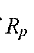 to
to


In systems where it is prohibitive to use an inductor to improve power output or when the series resistance of the piezoelectric harvester is high, a switch-only rectifier scheme can be used. FIG. 4 shows a schematic of an exemplary embodiment of the switch-only rectifier circuit 78 in accordance with the invention. The circuit 78 includes a regular full-bridge rectifier, having the diode arrangement 82, with the addition of a switch Φso.
The switch Φso helps in discharging the voltage across Cp from ±VRECT to ground when the input current changes direction. This way the charge lost in the full- bridge and voltage doubler cases can be reduced by half. This helps in increasing the
power output from the harvester 80 by 2X compared to a full-bridge rectifier or voltage doubler.
FIG. 5 shows an exemplary circuit architecture 30 which uses a bias-flip rectifier 34. The output of the rectifier 34 is fed to a main DC-DC converter 36 whose output is an energy buffer. The energy buffer can be a battery or a large storage capacitor This output can then feed a multiplicity of DC-DC converters


 each of which can cater to its own load circuitry V

Depending on the system being built, there can be many different DC-DC converters (buck/boost) DCDC_2-DCDC_N downstream or the system 30 might just have the main DC-DC converter 36. These DC-DC converters will themselves employ inductors.
The bias-flip rectifier can help improve the power extracted from piezoelectric harvesters by 6 - 8X. However, it requires the use of an inductor. In the proposed implementation here, this inductor can be the same one used in the many different DC-DC converters present in the system using the arbiter as shown in FIG. 5.
FIG. 6 shows a circuit architecture 40 with a bias-flip rectifier system 42. The output voltage of the rectifier V
 T needs to be regulated at its optimum point for maximal power transfer. A buck DC-DC converter 44 is used to regulate V and
 efficiently pass on the energy VSTO obtained to a storage capacitor CSTO or a rechargeable battery. A boost DC-DC converter 48 is used to generate a high voltage VHIGH (~5V) which is used to power the switches of the bias-flip rectifier 42. Both the buck and boost DC-DC converters 44,48 employ an inductor-based architecture for improved efficiency. The arbiter block 46 is used to control access to the shared inductor (LSHARE) which is shared between the bias-flip rectifier 42, buck and boost DC-DC converters 44, 48, as shown in FIG. 7.
Thus, effectively, the inductor
efficiently pass on the energy VSTO obtained to a storage capacitor CSTO or a rechargeable battery. A boost DC-DC converter 48 is used to generate a high voltage VHIGH (~5V) which is used to power the switches of the bias-flip rectifier 42. Both the buck and boost DC-DC converters 44,48 employ an inductor-based architecture for improved efficiency. The arbiter block 46 is used to control access to the shared inductor (LSHARE) which is shared between the bias-flip rectifier 42, buck and boost DC-DC converters 44, 48, as shown in FIG. 7.
Thus, effectively, the inductor
 can be time shared between the rectifier 42 and the many different DC-DC converters 44, 46. This is done with the help of the arbiter block 46 as shown in more detail in FIG. 6. The arbiter receives requests
 for usage of the inductor (LSHARE) from the rectifier 42 and the
 different DC-DC converters 44, 48. It then allocates the inductor (LSHARE) to the requestor if the inductor (LSIIΛRE) is unoccupied or enters the request into a queue if the inductor
 is occupied. The inductor (LSHARE) can be allocated to the different requestors using a FIFO approach or based on a priority scheme as needed. This inductor
 sharing approach requires the use of only one inductor for the entire system thereby minimizing area, volume and cost.
FIG. 8 shows an exemplary circuit architecture 56 including a bias-flip rectifier 60 having an inductor LQF that is connected in parallel with the PE harvester 58. The switches Ml and M2 are turned ON for a brief time when the PE current Ip crosses zero in either direction. When the switches Ml and M2 are ON, the inductor LBF helps in flipping the voltage VBF across CP . The series resistance along the
 Cp resonant path limits the magnitude of this voltage inversion. After the switches close, the PE current Ip needs to supply a smaller amount of charge to Cp to bring it up to This significantly improves the power extractable from the harvester
 58. The output power that can be obtained with the bias-flip rectifier can be given by Eq. 10.
The bias- flip switches Ml and M2 are turned ON when the current from the harvester 58 crosses zero. At this point one of the voltages VHΛR_P or VHAR_N is close to and the other one is close to zero. Let the maximum gate overdrive allowed by
 the technology in use be For most efficient charge transfer through the inductor
 LBF , the gate overdrive of the bias-flip switches Ml and M2 needs to be The
 gate-drive circuitry shown in FIGs. 9A-9B accomplishes this while maintaining the bias-flip switches Ml and M2 within breakdown limits.
In particular, FIG. 9A shows a circuit 66 that drives the bias flip transistor switch Ml of FIG. 7. The circuit 66 includes switches 68 that are closed at a respective pulse Φ, and switches 70 that are closed at a respective state Φ2 . FIG. 9B shows a circuit 70 that drives the bias flip transistor switch M2 of FIG. 7. The circuit 72 includes switches 74 that are closed at a respective pulse phase Φt and switches 76 that are closed at a respective pulse phase Φ2 . The gate-drive circuitries 66, 72 include a capacitor CGD which can be implemented on-chip. During phase when the bias-flip switches Ml and M2 are
 OFF, the capacitor CGD gets charged to
 and the gate voltages of both the bias- flip Ml and M2 switches are brought to ground. Wl] en Ip crosses zero the bias- flipping takes place, phase Φ2 begins, where the voltage across CGD remains almost the same, but the voltage referenced to ground at
 and
and
 T becomes (
 respectively. This turns ON the bias-flip switches Ml

 and M2 and keeps them ON till the flipping of voltage across C0 has taken place. After this, phase Φ2 ends and the bias-flip switches Ml and M2 are turned OFF. The voltage can be obtained using a boost DC-DC converter using the same shared
 inductor controlled by the arbiter. This simple scheme can be implemented on-chip and prevents the bias-flip switches from breaking down due to high voltage.
Although the present invention has been shown and described with respect to several preferred embodiments thereof, various changes, omissions and additions to the form and detail thereof, may be made therein, without departing from the spirit and scope of the invention. What is claimed is:
Claims
CLAIMS 1. An energy harvester circuit comprising: a harvesting module for extracting energy from an ambient source; a bias flip module for managing the manner in which voltage across said harvesting module transitions when input current to said harvesting module changes direction so as to allow a majority of the charge available from the harvesting module to be extracted; and a voltage transitioning module that is shared amongst one or more DC-DC converters for efficient energy management.
2. The energy harvester circuit of claim 1, wherein said one or more DC-DC converters comprising a main DC-DC converter coupled to one or more of secondary DC-DC converters.
3. The energy harvester circuit of claim 1, wherein said voltage transitioning module comprises an inductor mechanism or switching mechanism.
4. The energy harvester circuit of claim 3, wherein said inductor mechanism is shared amongst said main DC-DC converter and said one or more secondary DC-DC converters.
5. The energy harvester circuit of claim 3, wherein said inductor mechanism utilizes an arbiter to share inductance with said main DC-DC converter and said one or more secondary DC-DC converters
6. The energy harvester circuit of claim 1, wherein said voltage transitioning module comprises one or more switches.
7. The energy harvester circuit of claim 1, wherein said bias flip module is coupled to a capacitance at its output.
8. The energy harvester circuit of claim 1, wherein said bias flip module comprises a plurality of diodes.
9. The energy harvester circuit of claim 5, wherein said arbiter receives input signals from said bias flip module and said one or more DC-DC converters as to determining sharing of inductance.
10. The energy harvester circuit of claim 1, wherein said harvesting module comprises a piezoelectric harvester.
11. A method of performing energy harvesting comprising: providing a harvesting module for extracting energy from an ambient source; implementing a bias flip module for managing the manner in which voltage across said harvesting module transitions when input current to said harvesting module changes direction so as to allow a majority of the charge available from the harvesting module to be extracted; and implementing a voltage transitioning module that is shared amongst one or more DC-DC converters for efficient energy management.
12. The method of claim 11, wherein said one or more DC-DC converters comprising a main DC-DC converter coupled to one or more of secondary DC-DC converters.
13. The method of claim 1 1, wherein said voltage transitioning module comprises an inductor mechanism or switching mechanism.
14. The method of claim 13, wherein said inductor mechanism is shared amongst said main DC-DC converter and said one or more secondary DC-DC converters.
15. The method of claim 13, wherein said inductor mechanism utilizes an arbiter to share inductance with said main DC-DC converter and said one or more secondary DC-DC converters
16. The method of claim 11, wherein said voltage transitioning module comprises one or more switches.
17. The method of claim 1 1, wherein said bias flip module is coupled to a capacitance at its output.
18. The method of claim 11, wherein said bias flip module comprises a plurality of diodes.
19. The method of claim 15, wherein said arbiter receives input signals from said bias flip module and said one or more DC-DC converters as to determining sharing of inductance.
20. The method of claim 11, wherein said harvesting module comprises a piezoelectric harvester.
Applications Claiming Priority (2)
| Application Number | Priority Date | Filing Date | Title |
|---|---|---|---|
| US9887308P | 2008-09-22 | 2008-09-22 | |
| US61/098,873 | 2008-09-22 |
Publications (2)
| Publication Number | Publication Date |
|---|---|
| WO2010033449A2 true WO2010033449A2 (en) | 2010-03-25 |
| WO2010033449A3 WO2010033449A3 (en) | 2010-06-24 |
Family
ID=42040081
Family Applications (1)
| Application Number | Title | Priority Date | Filing Date |
|---|---|---|---|
| PCT/US2009/056792 Ceased WO2010033449A2 (en) | 2008-09-22 | 2009-09-14 | Circuit and method to improve energy harvesting efficiency in piezoelectric harvesters |
Country Status (2)
| Country | Link |
|---|---|
| US (1) | US8026650B2 (en) |
| WO (1) | WO2010033449A2 (en) |
Cited By (8)
| Publication number | Priority date | Publication date | Assignee | Title |
|---|---|---|---|---|
| CN102545691A (en) * | 2010-11-15 | 2012-07-04 | 精工爱普生株式会社 | Power generating device and electronic component |
| JP2012152009A (en) * | 2011-01-19 | 2012-08-09 | Seiko Epson Corp | Power generator, secondary battery, and electronic apparatus |
| CN103647463A (en) * | 2013-11-06 | 2014-03-19 | 大连理工大学 | Low-frequency and low-loss energy management chip based on piezoelectric effect |
| CN105490563A (en) * | 2016-01-21 | 2016-04-13 | 湖南大学 | Piezoelectric energy acquisition rectifier of short-circuit capacitance split structure |
| KR20160103391A (en) * | 2015-02-24 | 2016-09-01 | 서울대학교산학협력단 | Energy harvester and wireless switch using the same |
| US9888337B1 (en) | 2015-07-25 | 2018-02-06 | Gary M. Zalewski | Wireless coded communication (WCC) devices with power harvesting power sources for WiFi communication |
| US9911290B1 (en) | 2015-07-25 | 2018-03-06 | Gary M. Zalewski | Wireless coded communication (WCC) devices for tracking retail interactions with goods and association to user accounts |
| WO2019177346A1 (en) * | 2018-03-15 | 2019-09-19 | 주식회사 커널로그 | Energy harvesting apparatus capable of recycling remaining charges by using voltage supervisor |
Families Citing this family (26)
| Publication number | Priority date | Publication date | Assignee | Title |
|---|---|---|---|---|
| DE102010018293A1 (en) * | 2010-04-26 | 2011-10-27 | Siemens Aktiengesellschaft | Interface circuit for energy-self-sufficient system utilized for energy-self-sufficient pressure monitoring in vehicle tire, has control branches arranged in series with shift member, where circuit has free configurable voltage potential |
| US8368290B2 (en) | 2010-05-18 | 2013-02-05 | Georgia Tech Research Corporation | Rectifier-free piezoelectric energy harverster and battery charger |
| JP4835889B1 (en) * | 2010-11-18 | 2011-12-14 | セイコーエプソン株式会社 | Power generation device, electronic device and moving means |
| JP4811537B1 (en) * | 2011-02-17 | 2011-11-09 | セイコーエプソン株式会社 | Power generator |
| US8653718B2 (en) * | 2011-05-06 | 2014-02-18 | Seiko Epson Corporation | Power generation unit, electronic apparatus, transportation unit, battery, method of controlling power generation unit |
| JP5888486B2 (en) | 2011-10-03 | 2016-03-22 | セイコーエプソン株式会社 | Power generation device, power generation device control method, electronic device, and moving means |
| JP5879887B2 (en) | 2011-10-03 | 2016-03-08 | セイコーエプソン株式会社 | Power generator |
| US9048420B2 (en) | 2011-10-03 | 2015-06-02 | Seiko Epson Corporation | Power generation unit, electronic apparatus, transportation device, and method of controlling power generation unit |
| JP6015917B2 (en) | 2011-10-03 | 2016-10-26 | セイコーエプソン株式会社 | Power generation device, electronic device and moving means |
| US9112433B2 (en) | 2011-10-03 | 2015-08-18 | Seiko Epson Corporation | Power generation unit, battery, electronic apparatus, transportation device, and method of controlling power generation unit |
| JP5979369B2 (en) * | 2011-10-03 | 2016-08-24 | セイコーエプソン株式会社 | Power generation device, electronic device, moving means, battery, and method for controlling power generation device |
| US9344014B2 (en) * | 2012-09-05 | 2016-05-17 | Texas Instruments Incorporated | Piezoelectric device |
| JP5962412B2 (en) * | 2012-10-05 | 2016-08-03 | 株式会社ソシオネクスト | Bridge rectifier circuit |
| WO2015022794A1 (en) | 2013-08-13 | 2015-02-19 | 国立大学法人東北大学 | Power generating apparatus |
| WO2015111259A1 (en) | 2014-01-22 | 2015-07-30 | 株式会社村田製作所 | Piezoelectric power generation module and remote controller |
| WO2017014003A1 (en) * | 2015-07-17 | 2017-01-26 | 株式会社村田製作所 | Power generation device and electric apparatus provided with same |
| CN106100293B (en) * | 2016-08-24 | 2018-10-09 | 西安电子科技大学 | current detection circuit and piezoelectric rectifier applied to piezoelectric rectifier |
| TWI595750B (en) * | 2016-12-23 | 2017-08-11 | 德利威電子股份有限公司 | Two-way Trigger Type Piezo Device |
| CN108955866B (en) * | 2017-05-21 | 2023-11-07 | 天津大学(青岛)海洋工程研究院有限公司 | A piezoelectric vibration frequency sensor system based on bias flipping circuit |
| NL2019135B1 (en) * | 2017-06-28 | 2019-01-07 | Nowi Energy B V | An energy harvester to convert incident radio frequency, RF, energy associated with an RF signal to direct current energy as well as a corresponding method and sensor. |
| KR101870829B1 (en) * | 2017-07-07 | 2018-06-29 | 주식회사 커널로그 | An energy collecting device capable of reusing residual charge using a piezoelectric element |
| JP6842092B2 (en) * | 2018-05-31 | 2021-03-17 | 国立大学法人 東京大学 | Power supply circuit and vibration power generator |
| CN109039155B (en) * | 2018-08-15 | 2020-03-13 | 天津大学 | Self-adaptive bias flip circuit for piezoelectric energy collecting device |
| EP4068402B1 (en) | 2021-03-29 | 2023-03-22 | Cairdac | Module with optimised extraction of the energy from a piezoelectric transducer, in particular for recharging the battery of an implantable medical device such as a leadless autonomous cardiac capsule |
| KR102787103B1 (en) * | 2021-06-17 | 2025-03-26 | 한국전력공사 | Rectifier for energy harvester |
| KR102768985B1 (en) * | 2021-08-11 | 2025-02-19 | 한국전력공사 | Rectifier for energy harvester |
Family Cites Families (10)
| Publication number | Priority date | Publication date | Assignee | Title |
|---|---|---|---|---|
| GB1400101A (en) * | 1972-04-06 | 1975-07-16 | Suwa Seikosha Kk | Electronic oscillator circuit for a timepiece |
| JPH07245970A (en) * | 1994-03-02 | 1995-09-19 | Calsonic Corp | Piezoelectric power generator |
| US6522048B1 (en) * | 2001-08-20 | 2003-02-18 | Ocean Power Technologies, Inc. | Sensors for power conversion systems |
| US6528928B1 (en) * | 2001-08-20 | 2003-03-04 | Ocean Power Technologies, Inc. | Switched resonant power conversion electronics |
| US20030057778A1 (en) * | 2001-09-25 | 2003-03-27 | George Ai | Multiple DC control for single power supply |
| US6807853B2 (en) * | 2002-05-10 | 2004-10-26 | Michelin Recherche Et Technique S.A. | System and method for generating electric power from a rotating tire's mechanical energy using piezoelectric fiber composites |
| US20050285728A1 (en) * | 2004-06-29 | 2005-12-29 | Tyndall Patrick A | Power conversion from piezoelectric source |
| GB2425160B (en) | 2005-04-12 | 2010-11-17 | Perpetuum Ltd | An Electromechanical Generator for, and method of, Converting Mechanical Vibrational Energy into Electrical Energy |
| US7550873B2 (en) * | 2007-01-28 | 2009-06-23 | Ming Jiang | Uninterruptible power supply for home/office networking and communication system |
| US8129887B2 (en) * | 2009-01-30 | 2012-03-06 | The Curators Of The University Of Missouri | System and method for harvesting energy from environmental vibrations |
-
2009
- 2009-09-14 WO PCT/US2009/056792 patent/WO2010033449A2/en not_active Ceased
- 2009-09-14 US US12/558,820 patent/US8026650B2/en not_active Expired - Fee Related
Cited By (30)
| Publication number | Priority date | Publication date | Assignee | Title |
|---|---|---|---|---|
| CN102545691A (en) * | 2010-11-15 | 2012-07-04 | 精工爱普生株式会社 | Power generating device and electronic component |
| JP2012152009A (en) * | 2011-01-19 | 2012-08-09 | Seiko Epson Corp | Power generator, secondary battery, and electronic apparatus |
| CN103647463A (en) * | 2013-11-06 | 2014-03-19 | 大连理工大学 | Low-frequency and low-loss energy management chip based on piezoelectric effect |
| CN103647463B (en) * | 2013-11-06 | 2016-08-17 | 大连理工大学 | A kind of low frequency low-loss energy management chip based on piezoelectric effect |
| KR101696427B1 (en) * | 2015-02-24 | 2017-01-13 | 서울대학교산학협력단 | Energy harvester and wireless switch using the same |
| KR20160103391A (en) * | 2015-02-24 | 2016-09-01 | 서울대학교산학협력단 | Energy harvester and wireless switch using the same |
| WO2016137124A1 (en) * | 2015-02-24 | 2016-09-01 | 서울대학교산학협력단 | Energy collection apparatus and wireless switch using same |
| US10142822B1 (en) | 2015-07-25 | 2018-11-27 | Gary M. Zalewski | Wireless coded communication (WCC) devices with power harvesting power sources triggered with incidental mechanical forces |
| US10510219B1 (en) | 2015-07-25 | 2019-12-17 | Gary M. Zalewski | Machine learning methods and systems for managing retail store processes involving cashier-less transactions |
| US9888337B1 (en) | 2015-07-25 | 2018-02-06 | Gary M. Zalewski | Wireless coded communication (WCC) devices with power harvesting power sources for WiFi communication |
| US9894471B1 (en) | 2015-07-25 | 2018-02-13 | Gary M. Zalewski | Wireless coded communication (WCC) devices with power harvesting power sources for processing biometric identified functions |
| US9911290B1 (en) | 2015-07-25 | 2018-03-06 | Gary M. Zalewski | Wireless coded communication (WCC) devices for tracking retail interactions with goods and association to user accounts |
| US10038992B1 (en) | 2015-07-25 | 2018-07-31 | Gary M. Zalewski | Wireless coded communication (WCC) devices with power harvesting power sources used in switches |
| US10140820B1 (en) | 2015-07-25 | 2018-11-27 | Gary M. Zalewski | Devices for tracking retail interactions with goods and association to user accounts for cashier-less transactions |
| US11417179B1 (en) | 2015-07-25 | 2022-08-16 | Gary M. Zalewski | Using image and voice tracking to contextually respond to a user in a shopping environment |
| US10187773B1 (en) | 2015-07-25 | 2019-01-22 | Gary M. Zalewski | Wireless coded communication (WCC) devices with power harvesting power sources for monitoring state data of objects |
| US10355730B1 (en) | 2015-07-25 | 2019-07-16 | Gary M. Zalewski | Wireless coded communication (WCC) devices with power harvesting power sources for processing internet purchase transactions |
| US11315393B1 (en) | 2015-07-25 | 2022-04-26 | Gary M. Zalewski | Scenario characterization using machine learning user tracking and profiling for a cashier-less retail store |
| US11288933B1 (en) | 2015-07-25 | 2022-03-29 | Gary M. Zalewski | Devices for tracking retail interactions with goods and association to user accounts for cashier-less transactions |
| US10573134B1 (en) | 2015-07-25 | 2020-02-25 | Gary M. Zalewski | Machine learning methods and system for tracking label coded items in a retail store for cashier-less transactions |
| US10582358B1 (en) | 2015-07-25 | 2020-03-03 | Gary M. Zalewski | Wireless coded communication (WCC) devices with energy harvesting power functions for wireless communication |
| US10681518B1 (en) | 2015-07-25 | 2020-06-09 | Gary M. Zalewski | Batteryless energy harvesting state monitoring device |
| US10681519B1 (en) | 2015-07-25 | 2020-06-09 | Gary M. Zalewski | Methods for tracking shopping activity in a retail store having cashierless checkout |
| US10834562B1 (en) | 2015-07-25 | 2020-11-10 | Gary M. Zalewski | Lighting devices having wireless communication and built-in artificial intelligence bot |
| US10977907B1 (en) | 2015-07-25 | 2021-04-13 | Gary M. Zalewski | Devices for tracking retail interactions with goods including contextual voice input processing and artificial intelligent responses |
| US11195388B1 (en) | 2015-07-25 | 2021-12-07 | Gary M. Zalewski | Machine learning methods and systems for managing retail store processes involving the automatic gathering of items |
| CN105490563B (en) * | 2016-01-21 | 2018-01-16 | 湖南大学 | A kind of piezoelectric energy collection rectifier of short-circuit type electric capacity splitted construction |
| CN105490563A (en) * | 2016-01-21 | 2016-04-13 | 湖南大学 | Piezoelectric energy acquisition rectifier of short-circuit capacitance split structure |
| US11205904B2 (en) | 2018-03-15 | 2021-12-21 | Conalog Co., Ltd. | Energy collecting device capable of reusing residual charge using voltage supervisors |
| WO2019177346A1 (en) * | 2018-03-15 | 2019-09-19 | 주식회사 커널로그 | Energy harvesting apparatus capable of recycling remaining charges by using voltage supervisor |
Also Published As
| Publication number | Publication date |
|---|---|
| US8026650B2 (en) | 2011-09-27 |
| WO2010033449A3 (en) | 2010-06-24 |
| US20100079034A1 (en) | 2010-04-01 |
Similar Documents
| Publication | Publication Date | Title |
|---|---|---|
| US8026650B2 (en) | Circuit and method to improve energy harvesting efficiency in piezoelectric harvesters | |
| Shahzad et al. | Interleaved LLC converter with cascaded voltage-doubler rectifiers for deeply depleted PEV battery charging | |
| Ramadass et al. | An efficient piezoelectric energy harvesting interface circuit using a bias-flip rectifier and shared inductor | |
| CN109891354B (en) | Feedback control for efficient high-speed battery charging | |
| CN107689663B (en) | Battery Charging Architecture | |
| US10454291B2 (en) | DC-DC conversion for multi-cell batteries | |
| KR100723353B1 (en) | System to Control Power Delivery to DC Computer Components | |
| US9287792B2 (en) | Control method to reduce switching loss on MOSFET | |
| JP5674817B2 (en) | Battery charge equalization system | |
| KR101942970B1 (en) | Balancing method and battery system | |
| US20180175726A1 (en) | Hybrid DCDC Power Converter with Increased Efficiency | |
| CN110289757B (en) | Single inductance DC-DC converter with regulated output and energy harvesting system | |
| CN110417101B (en) | Battery charging circuit and battery charging method | |
| US8754545B2 (en) | High efficiency backup-power circuits for switch-mode power supplies | |
| US20140354247A1 (en) | Bridgeless pfc power converter with reduced emi noise | |
| EP3667865A1 (en) | Converter device and method | |
| JP4881952B2 (en) | DC / DC power converter | |
| US20130015820A1 (en) | System and method for balancing electrical energy storage devices via differential power bus and capacitive load switched-mode power supply | |
| US12463532B2 (en) | Multi-stage DC-DC converter | |
| EP3484042B1 (en) | Reconfigurable front end converter for full power energy storage applications | |
| US20160233697A1 (en) | Power storage device, power storage control device, and power storage control method | |
| Yang et al. | A quad-mode structure-reconfigurable regulating rectifier with shared-inductor DC–DC energy recycling in a wireless power receiver | |
| CN116261825A (en) | power supply circuit | |
| CN111211688A (en) | DC-DC converter and bidirectional DC-DC converter and uninterruptible power supply including the same | |
| Babenko et al. | DC/DC buck-boost converter with single inductance |
Legal Events
| Date | Code | Title | Description |
|---|---|---|---|
| 121 | Ep: the epo has been informed by wipo that ep was designated in this application |
Ref document number: 09815021 Country of ref document: EP Kind code of ref document: A2 |
|
| NENP | Non-entry into the national phase |
Ref country code: DE |
|
| 122 | Ep: pct application non-entry in european phase |
Ref document number: 09815021 Country of ref document: EP Kind code of ref document: A2 |