WO2009147719A1 - Test system - Google Patents
Test system Download PDFInfo
- Publication number
- WO2009147719A1 WO2009147719A1 PCT/JP2008/060171 JP2008060171W WO2009147719A1 WO 2009147719 A1 WO2009147719 A1 WO 2009147719A1 JP 2008060171 W JP2008060171 W JP 2008060171W WO 2009147719 A1 WO2009147719 A1 WO 2009147719A1
- Authority
- WO
- WIPO (PCT)
- Prior art keywords
- wafer
- semiconductor wafer
- test
- semiconductor
- alignment mark
- Prior art date
Links
Images


Classifications
-
- G—PHYSICS
- G01—MEASURING; TESTING
- G01R—MEASURING ELECTRIC VARIABLES; MEASURING MAGNETIC VARIABLES
- G01R31/00—Arrangements for testing electric properties; Arrangements for locating electric faults; Arrangements for electrical testing characterised by what is being tested not provided for elsewhere
- G01R31/28—Testing of electronic circuits, e.g. by signal tracer
- G01R31/2851—Testing of integrated circuits [IC]
- G01R31/2886—Features relating to contacting the IC under test, e.g. probe heads; chucks
- G01R31/2891—Features relating to contacting the IC under test, e.g. probe heads; chucks related to sensing or controlling of force, position, temperature
-
- H—ELECTRICITY
- H01—ELECTRIC ELEMENTS
- H01L—SEMICONDUCTOR DEVICES NOT COVERED BY CLASS H10
- H01L23/00—Details of semiconductor or other solid state devices
- H01L23/544—Marks applied to semiconductor devices or parts, e.g. registration marks, alignment structures, wafer maps
-
- H—ELECTRICITY
- H01—ELECTRIC ELEMENTS
- H01L—SEMICONDUCTOR DEVICES NOT COVERED BY CLASS H10
- H01L21/00—Processes or apparatus adapted for the manufacture or treatment of semiconductor or solid state devices or of parts thereof
- H01L21/67—Apparatus specially adapted for handling semiconductor or electric solid state devices during manufacture or treatment thereof; Apparatus specially adapted for handling wafers during manufacture or treatment of semiconductor or electric solid state devices or components ; Apparatus not specifically provided for elsewhere
- H01L21/68—Apparatus specially adapted for handling semiconductor or electric solid state devices during manufacture or treatment thereof; Apparatus specially adapted for handling wafers during manufacture or treatment of semiconductor or electric solid state devices or components ; Apparatus not specifically provided for elsewhere for positioning, orientation or alignment
-
- H—ELECTRICITY
- H01—ELECTRIC ELEMENTS
- H01L—SEMICONDUCTOR DEVICES NOT COVERED BY CLASS H10
- H01L2223/00—Details relating to semiconductor or other solid state devices covered by the group H01L23/00
- H01L2223/544—Marks applied to semiconductor devices or parts
- H01L2223/54453—Marks applied to semiconductor devices or parts for use prior to dicing
-
- H—ELECTRICITY
- H01—ELECTRIC ELEMENTS
- H01L—SEMICONDUCTOR DEVICES NOT COVERED BY CLASS H10
- H01L2924/00—Indexing scheme for arrangements or methods for connecting or disconnecting semiconductor or solid-state bodies as covered by H01L24/00
- H01L2924/0001—Technical content checked by a classifier
- H01L2924/0002—Not covered by any one of groups H01L24/00, H01L24/00 and H01L2224/00
Definitions
- the present invention relates to a test system for testing a semiconductor chip.
- the present invention relates to a test system for testing a plurality of semiconductor chips formed on a semiconductor wafer.
- the wafer under test and the probe card are unloaded from the inspection apparatus after the inspection is completed, and the wafer under test to be inspected next is adsorbed to the probe card. That is, not only the wafer to be tested but also the probe card must be unloaded from the inspection apparatus. For this reason, in the next test, both the alignment between the wafer under test and the probe card and the alignment of the probe card in the inspection apparatus must be adjusted. For this reason, the efficiency of a test will fall.
- an object of the present invention is to provide a test system that can solve the above problems. This object is achieved by a combination of features described in the independent claims.
- the dependent claims define further advantageous specific examples of the present invention.
- a test system for testing a plurality of semiconductor chips formed on a semiconductor wafer, the chamber in which the semiconductor wafer is transferred, and the fixing in the chamber A test wafer provided with a plurality of bumps that are electrically connected to a plurality of semiconductor chip pads at once and a semiconductor wafer placed in the chamber and moved to test the semiconductor wafer
- the semiconductor wafer is moved relative to the wafer stage so as to be placed on the wafer stage, the wafer stage being moved to a position opposite to the wafer, and the wafer stage.
- the position of the alignment mark provided on the semiconductor wafer is determined.
- a measuring unit for output, based on the position of the alignment mark measurement unit was measured, providing a test system comprising a position controller for adjusting the position of the placed semiconductor wafer on the wafer stage.
- a test system for testing a plurality of semiconductor chips formed on a semiconductor wafer, a chamber in which the semiconductor wafer is transferred, and a pad of the plurality of semiconductor chips fixed in the chamber. And a test wafer provided with a plurality of bumps that are electrically connected together and a semiconductor wafer placed and moved in the chamber to move the semiconductor wafer to a position facing the test wafer A wafer stage to be moved, and a measurement unit that is provided in a movement path of the wafer stage and detects the position of the alignment mark provided on the semiconductor wafer by scanning at least a part of the surface of the semiconductor wafer placed on the wafer stage And position control to adjust the position of the semiconductor wafer based on the position of the alignment mark measured by the measurement unit Providing a test system comprising and.
- FIG. 1 is a diagram showing an outline of a test system 400 according to one embodiment.
- 2 is a diagram for explaining an outline of a test in a test system 400.
- FIG. 5 is a diagram for explaining an example of a method for aligning a semiconductor wafer 300 at a predetermined position on a wafer stage 410.
- FIG. A part of the image scanned by the measurement unit 406 is shown.
- 2 is a diagram illustrating an example of an internal structure of a chamber 20.
- FIG. It is a figure explaining the example which detects the alignment mark 226 while the wafer stage 410 is moving. It is a figure explaining the other example which detects the alignment mark 226 while the wafer stage 410 is moving.
- 1 is an example of a cross-sectional view of a test wafer 100.
- FIG. 3 is a diagram illustrating a configuration example of a circuit unit 110.
- FIG. 2 is a diagram showing a configuration example in which a test wafer 100 and a semiconductor wafer
- ⁇ Logic comparison unit 140 ⁇ Characteristic measurement unit, 142 ⁇ Power supply unit, 150 ⁇ Intermediate pad, 204 ⁇ Support unit, 212 ⁇ ⁇ ⁇ Device-side anisotropic conductive sheet, 213 ⁇ Penetration , 214... Device side seal portion, 218... Wafer side anisotropic conductive sheet, 219... Through hole, 220... Fixing ring, 222. 226 ... alignment mark, 230 ... intake path, 232 ... intake path, 234 ... decompression section, 236 ... decompressor, 238 ... decompressor, 240 ... through-hole, 242 ... through hole, 300 ... semiconductor wafer, 310 ... semiconductor chip, 400 ... test system, 402 ...
- motherboard 404 ... performance board, 406 ... measurement unit, 407 ..Image sensor, 408... Wafer tray, 410... Wafer stage, 412... Horizontal stage, 416... Vertical stage, 418. Guide portion, wafer position detecting unit for 422 ... test, 450 ... position controller
- FIG. 1 is a diagram showing an outline of a test system 400 according to one embodiment.
- the test system 400 tests a plurality of semiconductor chips formed on the semiconductor wafer 300.
- the test system 400 may test a plurality of semiconductor wafers 300 in parallel.
- the test system 400 includes a control device 10, a plurality of chambers 20, a transfer unit 40, and a wafer cassette 60.
- the control device 10 controls the test system 400.
- the control device 10 may control the chamber 20, the transfer unit 40, and the wafer cassette 60.
- the chamber 20 sequentially receives the semiconductor wafers 300 to be tested and tests the semiconductor wafers 300 inside the chamber 20.
- Each chamber 20 may independently test the semiconductor wafer 300. That is, each chamber 20 may test the semiconductor wafer 300 without synchronizing with the other chambers 20.
- the wafer cassette 60 stores a plurality of semiconductor wafers 300.
- the transfer unit 40 sequentially transfers a plurality of semiconductor wafers 300 to be tested to the respective chambers 20. For example, the transfer unit 40 transfers each semiconductor wafer 300 stored in the wafer cassette 60 into one of the vacant chambers 20. Further, the transfer unit 40 may unload the semiconductor wafer 300 that has been tested from the chamber 20 and store it in the wafer cassette 60.
- FIG. 2 is a diagram for explaining the outline of the test in the test system 400.
- the test system 400 uses the test wafer 100 to test each semiconductor chip 310 of the semiconductor wafer 300.
- the test wafer 100 is previously installed in each chamber 20 shown in FIG.
- the test wafer 100 may be formed of the same semiconductor material as the semiconductor wafer 300 to be tested.
- the semiconductor wafer 300 may be a disk-shaped semiconductor wafer. More specifically, the semiconductor wafer 300 may be silicon, a compound semiconductor, or other semiconductor wafers.
- test wafer 100 may have substantially the same diameter as the semiconductor wafer 300 to be tested.
- the semiconductor wafer 300 is aligned at a predetermined position facing the test wafer 100 in the chamber 20. Then, by moving the semiconductor wafer 300 so as to overlap the test wafer 100, the plurality of wafer-side connection pads 112 of the test wafer 100 and the inspection pads of the plurality of semiconductor chips 310 are collectively collected. Electrically connected.
- the semiconductor wafer 300 is placed on a wafer stage in the chamber 20 and moved to a position facing the test wafer 100 by the wafer stage.
- the relative positions of the test wafer 100 and the wafer stage are adjusted in advance.
- the test system 400 may align the semiconductor wafer 300 at a predetermined position with respect to the test wafer 100 by placing the semiconductor wafer 300 at a predetermined position on the surface of the wafer stage.
- a plurality of pads corresponding to the pads of the semiconductor chip 310 may be formed on the surface of the test wafer 100 facing the semiconductor wafer 300.
- the test wafer 100 and the semiconductor wafer 300 may be electrically connected by direct contact, or may be electrically connected by non-contact coupling such as electrostatic coupling or inductive coupling. . Further, the test wafer 100 and the semiconductor wafer 300 may pass signals through the optical transmission path.
- the test wafer 100 may be electrically connected to the semiconductor wafer 300 to be tested to transmit a signal between the control device 10 and the semiconductor wafer 300.
- the semiconductor wafer 300 may supply the test signal generated by the control device 10 to each semiconductor chip 310 of the semiconductor wafer 300. Further, the test wafer 100 may transmit a signal output from each semiconductor chip 310 to the control device 10.
- the test wafer 100 may include a plurality of circuit units 110 corresponding to the plurality of semiconductor chips 310.
- the test wafer 100 may have a plurality of circuit units 110 in a one-to-one correspondence with the plurality of semiconductor chips 310.
- Each circuit unit 110 may generate a signal to be supplied to the corresponding semiconductor chip 310, and may process a signal output from the corresponding semiconductor chip 310.
- Each circuit unit 110 may independently test the corresponding semiconductor chip 310.
- the control device 10 may supply power supply power, a control signal, and the like to each circuit unit 110.
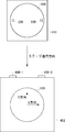
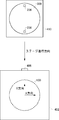
- FIG. 3 is a diagram for explaining an example of a method for aligning the semiconductor wafer 300 at a predetermined position on the wafer stage 410.
- FIG. 3 shows a top view of the wafer stage 410 and the semiconductor wafer 300.
- the test system 400 of this example includes a measurement unit 406 whose relative position with respect to the wafer stage 410 is predetermined.
- An alignment mark 226 is formed at a predetermined position on the semiconductor wafer 300.
- the measurement unit 406 scans at least a part of the surface of the semiconductor wafer 300 when the semiconductor wafer 300 is moving relative to the wafer stage 410 in order to place the semiconductor wafer 300 on the wafer stage 410.
- the position of the alignment mark provided on the semiconductor wafer 300 is detected.
- the measurement unit 406 is provided so as to image a predetermined fixed scan position in a region through which the semiconductor wafer 300 passes, and the semiconductor wafer 300 passes through the scan position, so that the surface of the semiconductor wafer 300 is detected. At least a portion may be scanned.
- the measurement unit 406 may image the semiconductor wafer 300 that is provided on the wafer stage 410 and passes above.
- the measurement unit 406 is provided above the wafer stage 410 and images the semiconductor wafer 300 that passes below. It's okay.
- the transfer unit 40 controls in advance the relative position of the handler that holds and moves the semiconductor wafer 300 with respect to the semiconductor wafer 300. Therefore, before the semiconductor wafer 300 is transferred into the chamber 20, the relative position between the semiconductor wafer 300 and the wafer stage 410 is generally adjusted. Using 406, the position of the semiconductor wafer 300 is finely adjusted.
- the measurement unit 406 is preferably provided at a position corresponding to the position of the alignment mark 226.
- the test system 400 may be given in advance the position of the alignment mark 226 on the semiconductor wafer 300. As described above, the relative position between the semiconductor wafer 300 and the wafer stage 410 is generally adjusted before the semiconductor wafer 300 is transferred into the chamber 20.
- the measurement unit 406 has an imaging range in a direction (hereinafter referred to as X direction) perpendicular to the traveling direction of the semiconductor wafer 300 (hereinafter referred to as Y direction). It may be provided to be smaller than the diameter.
- the imaging range in the X direction of the measurement unit 406 may be about 2 to 3 times the alignment mark 226.
- the measurement unit 406 includes a plurality of image sensors arranged at a predetermined pitch along the X direction so that the position of the alignment mark 226 in the X direction can be detected.
- the measurement unit 406 may be provided so that the position in the X direction can be changed.
- the test system 400 may change the position of the measurement unit 406 in the X direction based on position data of the alignment mark 226 given in advance.
- a plurality of measuring units 406 may be provided at different positions on the X-direction axis. In this case, since the positions of the plurality of alignment marks 226 can be detected, the position of the semiconductor wafer 300 can be detected with higher accuracy.
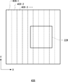
- FIG. 4 shows a part of an image scanned by the measurement unit 406.
- the measurement unit 406 since the measurement unit 406 includes the plurality of image sensors 407 along the X direction, the position of the alignment mark 226 in the X direction can be detected with a resolution corresponding to the pitch of the image sensors 407.
- the pitch of the imaging elements 407 is preferably smaller than the width of the alignment mark 226 in the X direction. Further, it is preferable that the pitch of the image pickup elements 407 is smaller than the allowable range of alignment errors determined according to the terminal widths of the semiconductor wafer 300 and the test wafer 100.
- the test system 400 detects the position of each alignment mark 226 in the X direction from the image captured by each measurement unit 406.
- the position control unit of the test system 400 may calculate the position in the Y direction of each alignment mark 226 based on the timing at which each measurement unit 406 detects each alignment mark 226. For example, the position control unit may detect the wafer stage based on how much the handler moves the semiconductor wafer 300 in the Y direction and places it on the wafer stage 410 after each measurement unit 406 detects the alignment mark 226. The position in the Y direction of the alignment mark 226 after the semiconductor wafer 300 is placed on 410 may be detected.
- the position control unit of the test system 400 may calculate the rotation amount of the semiconductor wafer 300 based on the position in the X direction and the position in the Y direction of each alignment mark 226 detected by the method described above. .
- the amount of rotation of the semiconductor wafer 300 indicates the amount of rotation of the semiconductor wafer 300 from its normal position around the center in a plane parallel to the wafer stage 410.
- the position control unit of the test system 400 may calculate the rotation angle between the detected position of each alignment mark 226 and the normal position of the alignment mark 226 given in advance.
- the rotation angle can be obtained from the difference between the detection position of the alignment mark 226 and the normal position of the alignment mark 226 in the X direction and the Y direction, and the distance from the center of the semiconductor wafer 300 to the alignment mark 226.
- the position controller of the test system 400 may be given a distance between the center of the semiconductor wafer 300 and the alignment mark 226 in advance.
- the position control unit of the test system 400 may control the wafer stage 410 based on the position in the X direction, the position in the Y direction, and the rotation amount of the alignment mark 226 detected by the method described above.
- Wafer stage 410 has a horizontal stage that can adjust the X direction, the Y direction, and the amount of rotation with semiconductor wafer 300 placed thereon. Further, the position control unit of the test system 400 controls the horizontal stage based on the position of the alignment mark 226 measured by the measurement unit 406, so that the X direction and Y direction of the semiconductor wafer 300 placed on the wafer stage 410 are controlled. The position and the amount of rotation may be adjusted.
- FIG. 5 is a diagram showing an example of the internal structure of the chamber 20.
- the semiconductor wafer 300 to be tested is sequentially transferred to the chamber 20 and is electrically connected to the test wafer 100 fixed in the chamber 20.
- a test wafer 100 Inside the chamber 20, a test wafer 100, a performance board 404, a mother board 402, a wafer tray 408, a wafer stage 410, a guide unit 420, a stage support unit 418, a measurement unit 406, and a position control unit 450 are provided.
- the test wafer 100 is fixed in the chamber 20.
- the test wafer 100 is fixed to the performance board 404 in the chamber 20.
- the performance board 404 may be a printed board on which wiring is formed, for example.
- the performance board 404 may be fixed to the mother board 402 in the chamber 20.
- the mother board 402 transmits a signal between the control device 10 and the test wafer 100 via the performance board 404.
- a membrane having a plurality of bumps is provided on the surface of the test wafer 100 that faces the semiconductor wafer 300.
- the test wafer 100 is electrically connected collectively to the pads of the plurality of semiconductor wafers 300 formed on the semiconductor wafer 300 by the plurality of bumps.
- the wafer stage 410 places and moves the semiconductor wafer 300 in the chamber 20.
- the semiconductor wafer 300 is fixed to the wafer tray 408 by suction or the like, and the wafer stage 410 places the wafer tray 408 thereon.
- Wafer stage 410 is connected to guide unit 420 via stage support unit 418 and moves along guide unit 420.
- the guide unit 420 moves the wafer stage 410 along a predetermined path between a receiving position A where the semiconductor wafer 300 is received from the transfer unit 40 and a predetermined position B facing the test wafer 100.
- the guide part 420 may be a rail provided along the predetermined route.
- the wafer stage 410 moves to a predetermined position B facing the test wafer 100, and then moves the semiconductor wafer 300 in the vertical direction so as to be electrically connected to the test wafer 100.
- the wafer stage 410 has a horizontal stage 412 and a vertical stage 416.
- the horizontal stage 412 mounts the wafer tray 408 and adjusts the position of the semiconductor wafer 300 in a plane parallel to the surface of the semiconductor wafer 300.
- the horizontal stage 412 adjusts the position of the semiconductor wafer 300 in the X and Y directions in the plane and the amount of rotation of the semiconductor wafer 300 in the plane. Thereby, the position of the semiconductor wafer 300 can be adjusted so that each pad of the semiconductor wafer 300 is electrically connected to each bump of the test wafer 100.
- the vertical stage 416 mounts the horizontal stage 412 and controls the position of the horizontal stage 412 in the vertical direction.
- the vertical stage 416 causes the semiconductor wafer 300 and the test wafer 100 to be electrically connected by bringing the horizontal stage 412 on which the semiconductor wafer 300 is placed close to the test wafer 100 at a position facing the test wafer 100. You may connect to.
- the vertical stage 416 brings the semiconductor wafer 300 close to the test wafer 100 to a predetermined distance, the space between the semiconductor wafer 300 and the test wafer 100 is depressurized, thereby the semiconductor wafer 300.
- the test wafer 100 may be electrically connected.
- a stage support 418 may be fixed to the vertical stage 416.
- the position control unit 450 controls the position of the wafer stage 410 based on the image captured by the measurement unit 406 as described with reference to FIG.
- the position controller 450 controls the position of the horizontal stage 412 to adjust the position of the semiconductor wafer 300 so that each pad of the semiconductor wafer 300 is disposed at a position corresponding to each bump of the test wafer 100. To do.
- the test wafer position detector 422 is fixed to the wafer stage 410 and measures the position of the test wafer 100 in advance.
- the test wafer position detection unit 422 may measure in advance the relative position in the horizontal plane of the alignment mark of the test wafer 100 with respect to the wafer stage 410 arranged at the predetermined position B. Since the position of the horizontal stage 412 varies in the horizontal plane, the test wafer position detection unit 422 is preferably provided on the vertical stage 416.
- the position controller 450 controls the horizontal stage 412 further based on the position of the test wafer 100 measured by the test wafer position detector 422 in order to connect the terminals of the test wafer 100 and the semiconductor wafer 300 with high accuracy. It's okay.
- the position of the semiconductor wafer 300 with respect to the test wafer 100 can be adjusted, and the plurality of terminals of the semiconductor wafer 300 and the plurality of terminals of the test wafer 100 can be electrically connected.
- the test wafer position detection unit 422 measures the position of the test wafer 100 every time the semiconductor wafer 300 is replaced. Not necessary.
- the test wafer position detection unit 422 may measure the position of the test wafer 100 for each predetermined period. For this reason, a plurality of semiconductor wafers 300 can be efficiently tested.
- the measurement unit 406 detects the position of the alignment mark 226 on the semiconductor wafer 300 while moving the semiconductor wafer 300 to place it on the wafer stage 410.
- the measurement unit 406 places the semiconductor wafer 300 on the wafer stage 410 and moves the position of the alignment mark 226 on the semiconductor wafer 300 while the wafer stage 410 is moving from position A to position B. It may be detected.
- the measurement unit 406 is provided on the moving path of the wafer stage 410 and scans at least a part of the surface of the semiconductor wafer 300 placed on the moving wafer stage 410.
- FIG. 6 is a diagram illustrating an example in which the alignment mark 226 is detected while the wafer stage 410 is moving.
- the measurement unit 406 of this example is fixed at a predetermined position with respect to the mother board 402 and images a part of the semiconductor wafer 300 passing below.
- the traveling direction of the wafer stage 410 is the Y direction
- the direction perpendicular to the traveling direction is the X direction.
- the measurement unit 406 detects an image similar to that of the measurement unit 406 described with reference to FIGS. Further, the position control unit 450 controls the horizontal stage 412 based on the image detected by the measurement unit 406.
- the position control unit 450 may detect the position of the alignment mark 226 in the Y direction based on the position of the wafer stage 410 in the Y direction when the measurement unit 406 detects the alignment mark 226.
- the position of the alignment mark 226 in the Y direction can be detected from the difference between the position in the Y direction of the wafer stage 410 when the measurement unit 406 detects the alignment mark 226 and the position B in the Y direction shown in FIG. it can.
- the position controller 450 adjusts the position of the horizontal stage 412 in the X direction and the Y direction and the amount of rotation based on the positions of the alignment marks 226 detected in this way in the X direction and the Y direction. As described above, even while the wafer stage 410 is moving, the position of the alignment mark 226 in the X direction and the Y direction can be detected and the position of the semiconductor wafer 300 can be adjusted.
- FIG. 7 is a diagram for explaining another example of detecting the alignment mark 226 while the wafer stage 410 is moving.
- the test system 400 of this example includes one measurement unit 406.
- the alignment mark 226 is similarly used using the single measuring unit 406. May be detected.
- the semiconductor wafer 300 may be provided with a plurality of alignment marks 226 at substantially the same position on the axis in the X direction, as shown in FIG.
- the measurement unit 406 is arranged so that the positions of these alignment marks 226 can be detected. Even with such a configuration, it is possible to detect a positional shift and a rotation amount of the semiconductor wafer 300 in the X direction and the Y direction.
- FIGS. 3 to 7 show the rectangular alignment mark 226 as an example, the shape of the alignment mark 226 is not limited to the shape.
- the alignment mark 226 may have a predetermined shape such as a cross. Further, the alignment mark 226 may have a plurality of pads arranged along a predetermined shape.
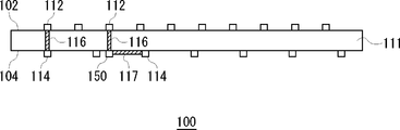
- FIG. 8 is an example of a cross-sectional view of the test wafer 100.
- the test wafer 100 of this example transmits signals between the control device 10 and the semiconductor wafer 300.
- the test wafer 100 includes a wafer side connection pad 112, an apparatus side connection pad 114, a through hole 116, an intermediate pad 150, and a wiring 117.
- the test wafer 100 has a wafer connection surface 102 and an apparatus connection surface 104 formed on the back surface of the wafer connection surface 102.
- Wafer connection surface 102 may refer to the surface facing semiconductor wafer 300.
- the device connection surface 104 may refer to a surface that is electrically connected to the control device 10.
- the plurality of wafer side connection pads 112 are formed on the wafer connection surface 102 of the test wafer 100. Further, at least one wafer side connection pad 112 is provided for each semiconductor chip 310. For example, one wafer side connection pad 112 may be provided for each input / output terminal of each semiconductor chip 310. That is, when each semiconductor chip 310 has a plurality of input / output terminals, a plurality of wafer side connection pads 112 may be provided for each semiconductor chip 310.
- the respective wafer side connection pads 112 are provided at the same intervals as the respective input / output terminals in the semiconductor wafer 300 and are electrically connected to the corresponding input / output terminals of the semiconductor chip 310.
- “electrically connected” may refer to a state in which an electric signal can be transmitted between two members.
- the wafer side connection pads 112 and the input / output terminals of the semiconductor chip 310 may be electrically connected by direct contact or indirectly through other conductors.
- the wafer side connection pads 112 of this example are electrically connected to the input / output terminals of the semiconductor chip 310 via a membrane described later in FIG. Bumps are formed on the membrane at positions corresponding to the pads.
- the input / output terminals of the wafer side connection pads 112 and the semiconductor chip 310 may be electrically connected in a non-contact state, such as capacitive coupling (electrostatic coupling) or inductive coupling (magnetic coupling). Further, a part of the transmission line between the wafer side connection pad 112 and the input / output terminal of the semiconductor chip 310 may be an optical transmission line.
- the plurality of device side connection pads 114 are formed on the device connection surface 104 of the test wafer 100 and are electrically connected to the performance board 404.
- the device side connection pads 114 are provided in one-to-one correspondence with the plurality of wafer side connection pads 112.
- the device side connection pads 114 are provided at the same intervals as the terminals of the performance board 404. Therefore, as shown in FIG. 8, the apparatus side connection pads 114 may be provided at a different interval from the wafer side connection pads 112.
- the through hole 116, the intermediate pad 150, and the wiring 117 are formed on the test wafer 100, and electrically connect the corresponding wafer side connection pad 112 and the apparatus side connection pad 114.
- the intermediate pad 150 is provided at a position facing the wafer side connection pad 112 on the apparatus connection surface 104.
- the through hole 116 is formed through the test wafer 100 so that one end is connected to the wafer side connection pad 112 and the other end is connected to the intermediate pad 150.
- the wiring 117 electrically connects the intermediate pad 150 and the device-side connection pad 114 on the device connection surface 104. With such a configuration, the apparatus side connection pads 114 and the wafer side connection pads 112 having different arrangement intervals are electrically connected.
- the wafer side connection pads 112 are arranged at the same intervals as the input terminals so as to be electrically connected to the input terminals of the semiconductor chip 310. For this reason, as shown in FIG. 2, for example, the wafer side connection pads 112 are provided in a predetermined region for each semiconductor chip 310 at a minute interval.
- the device-side connection pads 114 may be provided at intervals wider than the intervals between the plurality of wafer-side connection pads 112 corresponding to one semiconductor chip 310.
- the device side connection pads 114 may be arranged at equal intervals in the surface of the device connection surface 104 so that the distribution of the device side connection pads 114 is substantially uniform.
- test wafer 100 of this example is formed of the same semiconductor material as that of the semiconductor wafer 300, the electrical connection between the test wafer 100 and the semiconductor wafer 300 can be achieved even when the ambient temperature varies. Connection can be maintained well. For this reason, for example, even when the test is performed by heating the semiconductor wafer 300, the semiconductor wafer 300 can be accurately tested.
- the test wafer 100 is formed of a semiconductor material, a large number of wafer side connection pads 112 and the like can be easily formed on the test wafer 100.
- the wafer-side connection pad 112, the device-side connection pad 114, the through hole 116, and the wiring 117 can be easily formed by a semiconductor process using exposure or the like. Therefore, a large number of wafer side connection pads 112 corresponding to a large number of semiconductor chips 310 can be easily formed on the test wafer 100.
- the terminals of the test wafer 100 may be formed by plating, evaporating, or the like on the test wafer 100 with a conductive material.
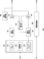
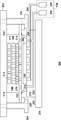
- FIG. 9 is a diagram illustrating a configuration example of the circuit unit 110.
- the circuit unit 110 includes a pattern generation unit 122, a waveform shaping unit 130, a driver 132, a comparator 134, a timing generation unit 136, a logic comparison unit 138, a characteristic measurement unit 140, and a power supply unit 142.
- the circuit unit 110 may have the configuration shown in FIG. 9 for each input / output pin of the semiconductor chip 310 to be connected.
- the pattern generator 122 generates a logic pattern of the test signal.
- the pattern generation unit 122 of this example includes a pattern memory 124, an expected value memory 126, and a fail memory 128.
- the pattern generator 122 may output a logical pattern stored in advance in the pattern memory 124.
- the pattern memory 124 may store a logical pattern given from the control device 10 before starting the test.
- the pattern generator 122 may generate the logical pattern based on an algorithm given in advance.
- the waveform shaping unit 130 shapes the waveform of the test signal based on the logical pattern given from the pattern generation unit 122.
- the waveform shaping unit 130 may shape the waveform of the test signal by outputting a voltage corresponding to each logic value of the logic pattern for each predetermined bit period.
- the driver 132 outputs a test signal corresponding to the waveform given from the waveform shaping unit 130.
- the driver 132 may output a test signal in accordance with the timing signal given from the timing generator 136.
- the driver 132 may output a test signal having the same cycle as the timing signal.
- the test signal output from the driver 132 is supplied to the corresponding semiconductor chip 310 via a switching unit or the like.
- the comparator 134 measures the response signal output from the semiconductor chip 310.
- the comparator 134 may measure the logical pattern of the response signal by sequentially detecting the logical value of the response signal in accordance with the strobe signal supplied from the timing generator 136.
- the logic comparison unit 138 functions as a determination unit that determines the quality of the corresponding semiconductor chip 310 based on the logic pattern of the response signal measured by the comparator 134. For example, the logic comparison unit 138 may determine the quality of the semiconductor chip 310 based on whether or not the expected value pattern given from the pattern generation unit 122 matches the logic pattern detected by the comparator 134.
- the pattern generation unit 122 may supply the expected value pattern stored in advance in the expected value memory 126 to the logic comparison unit 138.
- the expected value memory 126 may store a logic pattern given from the control device 10 before the test is started.
- the pattern generation unit 122 may generate the expected value pattern based on an algorithm given in advance.
- the fail memory 128 stores the comparison result in the logical comparison unit 138.
- the fail memory 128 may store the pass / fail judgment result in the logic comparison unit 138 for each address of the semiconductor chip 310.
- the control device 10 may read the pass / fail judgment result stored in the fail memory 128.
- the apparatus-side connection pad 114 may output the pass / fail determination result stored in the fail memory 128 to the control apparatus 10 outside the test wafer 100.
- the characteristic measurement unit 140 measures the voltage or current waveform output by the driver 132.
- the characteristic measurement unit 140 may function as a determination unit that determines whether the semiconductor chip 310 is good or not based on whether a waveform of a current or voltage supplied from the driver 132 to the semiconductor chip 310 satisfies a predetermined specification. .
- the power supply unit 142 supplies power for driving the semiconductor chip 310.
- the power supply unit 142 may supply power to the semiconductor chip 310 according to the power supplied from the control device 10 during the test. Further, the power supply unit 142 may supply driving power to each component of the circuit unit 110.
- the test system 400 in which the scale of the control device 10 is reduced can be realized.
- a general-purpose personal computer or the like can be used as the control device 10.
- FIG. 10 is a diagram illustrating a configuration example in which the test wafer 100 and the semiconductor wafer 300 are electrically connected.
- the test system 400 of this example places the test wafer 100 and the semiconductor wafer 300 in a sealed space, and depressurizes the sealed space, thereby bringing the test wafer 100 and the semiconductor wafer 300 close to each other and making electrical Connect to.
- a sealed space is formed between the performance board 404 to which the test wafer 100 is fixed and the wafer tray 408 on which the semiconductor wafer 300 is placed.
- An anisotropic conductive sheet is provided between the performance board 404, the test wafer 100, and the semiconductor wafer 300. Then, by reducing the pressure in the sealed space, the anisotropic conductive sheet is pressed by the test wafer 100 or the like, and the test wafer 100 or the like is electrically connected. Therefore, the test wafer 100 is fixed to the performance board 404 so as to be movable in the vertical direction.
- the range in which the test wafer 100 can be moved in the horizontal direction is preferably within an allowable range of alignment error between the test wafer 100 and the semiconductor wafer 300.
- the range in which the test wafer 100 can move in the horizontal direction is preferably sufficiently smaller than the pad width of the test wafer 100 and the semiconductor wafer 300.
- the test wafer 100 is fixed to the performance board 404 by the support unit 204.
- the support unit 204 fixes the device-side anisotropic conductive sheet 212, the device-side seal 214, the test wafer 100, the wafer-side anisotropic conductive sheet 218, the membrane 222, and the fixing ring 220 to the performance board 404.
- the apparatus-side anisotropic conductive sheet 212 is provided between the test wafer 100 and the performance board 404 and is electrically pressed to electrically connect the electrode of the test wafer 100 and the electrode of the performance board 404. .
- the test wafer 100 presses the apparatus-side anisotropic conductive sheet 212 so that the position in the vertical direction with respect to the lower surface of the performance board 404 can be displaced within a predetermined range to the extent that it can be electrically connected to the performance board 404. Supported.
- the device-side seal 214 is provided along the periphery of the surface of the membrane 222 on the performance board 404 side, and seals between the periphery of the surface of the membrane 222 on the performance board 404 side and the performance board 404.
- the device-side seal portion 214 may be formed of an elastic material having elasticity to the extent that the membrane 222 can be electrically connected to the performance board 404 via the device-side anisotropic conductive sheet 212.
- the wafer side anisotropic conductive sheet 218 is provided between the test wafer 100 and the membrane 222.
- the wafer side anisotropic conductive sheet 218 is pressed, the wafer side connection terminal provided on the surface of the test wafer 100 on the semiconductor wafer 300 side and the bump terminal of the membrane 222 are electrically connected.
- the membrane 222 is provided between the wafer side anisotropic conductive sheet 218 and the semiconductor wafer 300.
- the membrane 222 may have bump terminals that electrically connect the terminals of the semiconductor wafer 300 and the wafer-side connection terminals of the test wafer 100.
- the fixing ring 220 fixes the membrane 222 to the device-side seal portion 214.
- the fixing ring 220 may be provided in an annular shape along the peripheral edge of the surface of the membrane 222 on the semiconductor wafer 300 side.
- the inner diameter of the fixing ring 220 may be larger than the diameters of the wafer side anisotropic conductive sheet 218 and the semiconductor wafer 300.
- the membrane 222 has a circular shape having substantially the same diameter as that of the fixing ring 220, and an end portion thereof is fixed to the fixing ring 220.
- the apparatus-side anisotropic conductive sheet 212, the test wafer 100, and the wafer-side anisotropic conductive sheet 218 are disposed between the membrane 222 and the performance board 404. Held in position. As shown in FIG. 10, a gap may be provided between the apparatus-side anisotropic conductive sheet 212, the test wafer 100, the wafer-side anisotropic conductive sheet 218, and the apparatus-side seal portion 214. . With such a configuration, the semiconductor wafer 300 and the test wafer 100 can be electrically connected by pressing the membrane 222 with the semiconductor wafer 300.
- the support unit 204 may support the membrane 222 and the like by supporting the fixing ring 220.
- the support unit 204 supports the test wafer 100 so that the membrane 222 can approach the lower surface of the performance board 404 within a predetermined range.
- the support unit 204 supports the lower end of the fixing ring 220 at a position away from the lower surface of the performance board 404 by a predetermined distance so that the lower end of the fixing ring 220 cannot exceed a predetermined distance from the lower surface of the performance board 404. You can do it.
- the wafer tray 408 is provided so as to form a sealed space with the performance board 404 when placed at a predetermined position.
- the wafer tray 408 of this example forms a sealed space with the performance board 404, the apparatus-side seal 214, and the wafer-side seal 224.
- the wafer tray 408 places the semiconductor wafer 300 on the surface of the sealed space side.
- the wafer side seal portion 224 is provided along the region corresponding to the peripheral portion of the membrane 222 on the surface of the wafer tray 408, and seals between the peripheral portion of the surface of the membrane 222 on the wafer tray side and the wafer tray 408.
- the wafer side seal portion 224 may be formed in an annular shape on the surface of the wafer tray 408.
- the wafer-side seal portion 224 may be formed in a lip shape in which the annular diameter increases as the distance from the surface of the wafer tray 408 increases.
- the tip of the wafer-side seal portion 224 bends according to the pressing force, thereby bringing the distance between the membrane 222 and the semiconductor wafer 300 closer.
- the wafer-side seal portion 224 is formed so that the height from the surface of the wafer tray 408 is higher than the height of the semiconductor wafer 300 when not pressed against the membrane 222.
- the vertical stage 416 described with reference to FIG. 5 moves the wafer tray 408 to a position where the upper end portion of the wafer-side seal portion 224 is in close contact with the membrane 222.
- the performance board 404, the wafer tray 408, the apparatus-side seal portion 214, and the wafer-side seal portion 224 can form a sealed space in which the test wafer 100 and the semiconductor wafer 300 are stored.
- the horizontal stage 412 preferably adjusts the position and inclination of the semiconductor wafer 300 in the horizontal plane before the vertical stage 416 moves the wafer tray 408 in the vertical direction.
- the decompression unit 234 decompresses the sealed space between the performance board 404 and the wafer tray 408, which is formed by the performance board 404, the wafer tray 408, the apparatus side seal unit 214, and the wafer side seal unit 224.
- the decompression unit 234 decompresses the sealed space after the wafer stage 410 moves the wafer tray 408 to form the sealed space.
- the decompression unit 234 moves the wafer tray 408 closer to the performance board 404 to a predetermined position.
- the wafer tray 408 is disposed at the predetermined position, thereby applying a pressing force to the apparatus-side anisotropic conductive sheet 212 and the wafer-side anisotropic conductive sheet 218 to electrically connect the performance board 404 and the test wafer 100.
- the test wafer 100 and the semiconductor wafer 300 are electrically connected.
- the wafer side seal portion 224 may contact the membrane 222 inside the fixing ring 220.
- the membrane 222 divides the sealed space into a space on the performance board 404 side and a space on the wafer tray 408 side. For this reason, it is preferable that the membrane 222 is provided with a through hole 242 connecting these spaces.
- the test wafer 100, the apparatus-side anisotropic conductive sheet 212, and the wafer-side anisotropic conductive sheet 218 are also provided with a through hole 240, a through hole 213, and a through hole 219.
- the through-holes provided in the membrane 222, the test wafer 100, the apparatus-side anisotropic conductive sheet 212, and the wafer-side anisotropic conductive sheet 218 are preferably distributed substantially uniformly in each plane. With such a configuration, the air sucked in the process of depressurizing the sealed space flows in a dispersed manner through the many through holes.
- the through hole 242, the through hole 240, the through hole 213, and the through hole 219 may be provided at corresponding positions, or may be provided at different positions.
- the pressing force applied to the apparatus-side anisotropic conductive sheet 212 and the wafer-side anisotropic conductive sheet 218 is distributed substantially evenly in the respective planes. Stress strain can be greatly reduced. For this reason, it is possible to prevent cracking of the test wafer 100, distortion of the anisotropic conductive sheet, and the like.
- the space between the performance board 404 and the membrane 222 and the space between the membrane 222 and the semiconductor wafer 300 can be decompressed with a single decompression unit 234.
- the decompression unit 234 may adsorb the semiconductor wafer 300 to the wafer tray 408.
- the decompression unit 234 of this example includes a decompressor 236 for a sealed space and a decompressor 238 for a semiconductor wafer.
- the wafer tray 408 is formed with an air intake path 232 for a sealed space and an air intake path 230 for a semiconductor wafer.
- the test wafer 100 fixed to the performance board 404 and the semiconductor wafer 300 can be electrically connected. As described above, since the test wafer 100 is fixed to the performance board 404, alignment between the test wafer 100 and the semiconductor wafer 300 can be easily performed.
Abstract
A test system comprising a chamber into which a semiconductor wafer (300) is carried in, a test wafer which is fixed inside the chamber and is formed with a plurality of bumps to be collectively electrically connected to pads of a plurality of semiconductor chips formed on the semiconductor wafer, a wafer stage (410) which moves with the semiconductor wafer placed thereon to move the semiconductor wafer to a position facing the test wafer in the chamber, a measuring portion (406) which is disposed at a predetermined site with respect to the wafer stage and detects the position of an alignment mark (226) formed on the semiconductor wafer by scanning at least part of the surface of the semiconductor wafer while the semiconductor wafer is moved with respect to the wafer stage to be placed on the wafer stage, and a position controlling portion for adjusting the position of the semiconductor wafer placed on the wafer stage based on the position of the alignment mark measured by the measuring portion. This test system permits efficient alignment.
Description
本発明は、半導体チップを試験する試験システムに関する。特に本発明は、半導体ウエハに形成された複数の半導体チップを試験する試験システムに関する。
The present invention relates to a test system for testing a semiconductor chip. In particular, the present invention relates to a test system for testing a plurality of semiconductor chips formed on a semiconductor wafer.
半導体ウエハに形成された複数の半導体チップを試験する装置として、ウエハ上の多数のパッド電極に対して一括してコンタクトできるプローブカードを用いた装置が知られている(例えば、特許文献1参照)。当該装置は、プローブカードと、被試験ウエハとを一体に吸着させた状態で検査装置に投入して、高温中での検査等を行う。
特開2006-173503号公報
As an apparatus for testing a plurality of semiconductor chips formed on a semiconductor wafer, an apparatus using a probe card that can collectively contact a large number of pad electrodes on the wafer is known (see, for example, Patent Document 1). . In this apparatus, the probe card and the wafer to be tested are sucked together and put into an inspection apparatus to perform inspection at a high temperature.
JP 2006-173503 A
しかし、上述した装置では、検査終了後に被試験ウエハおよびプローブカードを検査装置から搬出して、次に検査すべき被試験ウエハを、当該プローブカードに吸着させる。つまり、被試験ウエハだけでなく、プローブカードも検査装置から搬出しなければならない。このため、次の試験では、被試験ウエハおよびプローブカード間のアライメントと、検査装置内におけるプローブカードのアライメントの双方を調整しなければならない。このため、試験の効率が低下してしまう。
However, in the apparatus described above, the wafer under test and the probe card are unloaded from the inspection apparatus after the inspection is completed, and the wafer under test to be inspected next is adsorbed to the probe card. That is, not only the wafer to be tested but also the probe card must be unloaded from the inspection apparatus. For this reason, in the next test, both the alignment between the wafer under test and the probe card and the alignment of the probe card in the inspection apparatus must be adjusted. For this reason, the efficiency of a test will fall.
そこで本発明は、上記の課題を解決することのできる試験システムを提供することを目的とする。この目的は請求の範囲における独立項に記載の特徴の組み合わせにより達成される。また従属項は本発明の更なる有利な具体例を規定する。
Therefore, an object of the present invention is to provide a test system that can solve the above problems. This object is achieved by a combination of features described in the independent claims. The dependent claims define further advantageous specific examples of the present invention.
上記課題を解決するために、本発明の第1の形態においては、半導体ウエハに形成された複数の半導体チップを試験する試験システムであって、半導体ウエハが搬送されるチャンバと、チャンバ内において固定され、複数の半導体チップのパッドと一括して電気的に接続される複数のバンプが設けられた試験用ウエハと、チャンバ内において、半導体ウエハを載置して移動することで、半導体ウエハを試験用ウエハと対向する位置に移動させるウエハステージと、ウエハステージに対して所定の位置に設けられ、半導体ウエハをウエハステージに載置すべく、ウエハステージに対して半導体ウエハが移動しているときに、半導体ウエハの表面の少なくとも一部をスキャンすることで、半導体ウエハに設けられたアライメントマークの位置を検出する測定部と、測定部が測定したアライメントマークの位置に基づいて、ウエハステージに載置された半導体ウエハの位置を調整する位置制御部とを備える試験システムを提供する。
In order to solve the above-described problem, in a first embodiment of the present invention, a test system for testing a plurality of semiconductor chips formed on a semiconductor wafer, the chamber in which the semiconductor wafer is transferred, and the fixing in the chamber A test wafer provided with a plurality of bumps that are electrically connected to a plurality of semiconductor chip pads at once and a semiconductor wafer placed in the chamber and moved to test the semiconductor wafer When the semiconductor wafer is moved relative to the wafer stage so as to be placed on the wafer stage, the wafer stage being moved to a position opposite to the wafer, and the wafer stage. By scanning at least a part of the surface of the semiconductor wafer, the position of the alignment mark provided on the semiconductor wafer is determined. A measuring unit for output, based on the position of the alignment mark measurement unit was measured, providing a test system comprising a position controller for adjusting the position of the placed semiconductor wafer on the wafer stage.
本発明の第2の形態においては、半導体ウエハに形成された複数の半導体チップを試験する試験システムであって、半導体ウエハが搬送されるチャンバと、チャンバ内において固定され、複数の半導体チップのパッドと一括して電気的に接続される複数のバンプが設けられた試験用ウエハと、チャンバ内において、半導体ウエハを載置して移動することで、半導体ウエハを試験用ウエハと対向する位置に移動させるウエハステージと、ウエハステージの移動経路に設けられ、ウエハステージに載置された半導体ウエハの表面の少なくとも一部をスキャンすることで、半導体ウエハに設けられたアライメントマークの位置を検出する測定部と、測定部が測定したアライメントマークの位置に基づいて、半導体ウエハの位置を調整する位置制御部とを備える試験システムを提供する。
According to a second aspect of the present invention, there is provided a test system for testing a plurality of semiconductor chips formed on a semiconductor wafer, a chamber in which the semiconductor wafer is transferred, and a pad of the plurality of semiconductor chips fixed in the chamber. And a test wafer provided with a plurality of bumps that are electrically connected together and a semiconductor wafer placed and moved in the chamber to move the semiconductor wafer to a position facing the test wafer A wafer stage to be moved, and a measurement unit that is provided in a movement path of the wafer stage and detects the position of the alignment mark provided on the semiconductor wafer by scanning at least a part of the surface of the semiconductor wafer placed on the wafer stage And position control to adjust the position of the semiconductor wafer based on the position of the alignment mark measured by the measurement unit Providing a test system comprising and.
なお、上記の発明の概要は、発明の必要な特徴の全てを列挙したものではなく、これらの特徴群のサブコンビネーションもまた、発明となりうる。
It should be noted that the above summary of the invention does not enumerate all the necessary features of the invention, and sub-combinations of these feature groups can also be the invention.
10・・・制御装置、20・・・チャンバ、40・・・搬送部、60・・・ウエハカセット、100・・・試験用ウエハ、102・・・ウエハ接続面、104・・・装置接続面、110・・・回路部、112・・・ウエハ側接続パッド、114・・・装置側接続パッド、116・・・スルーホール、117・・・配線、122・・・パターン発生部、124・・・パターンメモリ、126・・・期待値メモリ、128・・・フェイルメモリ、130・・・波形成形部、132・・・ドライバ、134・・・コンパレータ、136・・・タイミング発生部、138・・・論理比較部、140・・・特性測定部、142・・・電源供給部、150・・・中間パッド、204・・・支持部、212・・・装置側異方性導電シート、213・・・貫通孔、214・・・装置側シール部、218・・・ウエハ側異方性導電シート、219・・・貫通孔、220・・・固定リング、222・・・メンブレン、224・・・ウエハ側シール部、226・・・アライメントマーク、230・・・吸気経路、232・・・吸気経路、234・・・減圧部、236・・・減圧器、238・・・減圧器、240・・・貫通孔、242・・・貫通孔、300・・・半導体ウエハ、310・・・半導体チップ、400・・・試験システム、402・・・マザーボード、404・・・パフォーマンスボード、406・・・測定部、407・・・撮像素子、408・・・ウエハトレイ、410・・・ウエハステージ、412・・・水平ステージ、416・・・垂直ステージ、418・・・ステージ支持部、420・・・ガイド部、422・・・試験用ウエハ位置検出部、450・・・位置制御部
DESCRIPTION OF SYMBOLS 10 ... Control apparatus, 20 ... Chamber, 40 ... Transfer part, 60 ... Wafer cassette, 100 ... Test wafer, 102 ... Wafer connection surface, 104 ... Device connection surface , 110 ... Circuit part, 112 ... Wafer side connection pad, 114 ... Device side connection pad, 116 ... Through hole, 117 ... Wiring, 122 ... Pattern generation part, 124 ... Pattern memory 126 ... Expected value memory 128 ... Fail memory 130 ... Waveform shaping unit 132 ... Driver 134 ... Comparator 136 ... Timing generating unit 138 ... · Logic comparison unit, 140 ··· Characteristic measurement unit, 142 ··· Power supply unit, 150 ··· Intermediate pad, 204 ··· Support unit, 212 · · · Device-side anisotropic conductive sheet, 213・ Penetration , 214... Device side seal portion, 218... Wafer side anisotropic conductive sheet, 219... Through hole, 220... Fixing ring, 222. 226 ... alignment mark, 230 ... intake path, 232 ... intake path, 234 ... decompression section, 236 ... decompressor, 238 ... decompressor, 240 ... through-hole, 242 ... through hole, 300 ... semiconductor wafer, 310 ... semiconductor chip, 400 ... test system, 402 ... motherboard, 404 ... performance board, 406 ... measurement unit, 407 ..Image sensor, 408... Wafer tray, 410... Wafer stage, 412... Horizontal stage, 416... Vertical stage, 418. Guide portion, wafer position detecting unit for 422 ... test, 450 ... position controller
以下、発明の実施の形態を通じて本発明を説明するが、以下の実施形態は請求の範囲にかかる発明を限定するものではない。また、実施形態の中で説明されている特徴の組み合わせの全てが発明の解決手段に必須であるとは限らない。
Hereinafter, the present invention will be described through embodiments of the invention. However, the following embodiments do not limit the invention according to the claims. In addition, not all the combinations of features described in the embodiments are essential for the solving means of the invention.
図1は、一つの実施形態に係る試験システム400の概要を示す図である。試験システム400は、半導体ウエハ300に形成される複数の半導体チップを試験する。また、試験システム400は、複数の半導体ウエハ300を並列に試験してよい。試験システム400は、制御装置10、複数のチャンバ20、搬送部40、および、ウエハカセット60を備える。
FIG. 1 is a diagram showing an outline of a test system 400 according to one embodiment. The test system 400 tests a plurality of semiconductor chips formed on the semiconductor wafer 300. The test system 400 may test a plurality of semiconductor wafers 300 in parallel. The test system 400 includes a control device 10, a plurality of chambers 20, a transfer unit 40, and a wafer cassette 60.
制御装置10は、試験システム400を制御する。例えば制御装置10は、チャンバ20、搬送部40、および、ウエハカセット60を制御してよい。チャンバ20は、試験すべき半導体ウエハ300を順次受け取り、チャンバ20の内部で半導体ウエハ300を試験する。それぞれのチャンバ20は、独立に半導体ウエハ300を試験してよい。つまり、それぞれのチャンバ20は、他のチャンバ20と同期せずに、半導体ウエハ300を試験してよい。
The control device 10 controls the test system 400. For example, the control device 10 may control the chamber 20, the transfer unit 40, and the wafer cassette 60. The chamber 20 sequentially receives the semiconductor wafers 300 to be tested and tests the semiconductor wafers 300 inside the chamber 20. Each chamber 20 may independently test the semiconductor wafer 300. That is, each chamber 20 may test the semiconductor wafer 300 without synchronizing with the other chambers 20.
ウエハカセット60は、複数の半導体ウエハ300を格納する。搬送部40は、試験すべき複数の半導体ウエハ300を、それぞれのチャンバ20に順次搬送する。例えば搬送部40は、ウエハカセット60が格納したそれぞれの半導体ウエハ300を、空いているいずれかのチャンバ20内に搬送する。また、搬送部40は、試験が終了した半導体ウエハ300を、チャンバ20から搬出してウエハカセット60に格納してよい。
The wafer cassette 60 stores a plurality of semiconductor wafers 300. The transfer unit 40 sequentially transfers a plurality of semiconductor wafers 300 to be tested to the respective chambers 20. For example, the transfer unit 40 transfers each semiconductor wafer 300 stored in the wafer cassette 60 into one of the vacant chambers 20. Further, the transfer unit 40 may unload the semiconductor wafer 300 that has been tested from the chamber 20 and store it in the wafer cassette 60.
図2は、試験システム400における試験の概要を説明する図である。試験システム400は、試験用ウエハ100を用いて、半導体ウエハ300のそれぞれの半導体チップ310を試験する。試験用ウエハ100は、図1に示したそれぞれのチャンバ20内に、予め設置される。
FIG. 2 is a diagram for explaining the outline of the test in the test system 400. The test system 400 uses the test wafer 100 to test each semiconductor chip 310 of the semiconductor wafer 300. The test wafer 100 is previously installed in each chamber 20 shown in FIG.
試験用ウエハ100は、試験対象の半導体ウエハ300と同一の半導体材料で形成されてよい。例えば、半導体ウエハ300は、円盤状の半導体ウエハであってよい。より具体的には、半導体ウエハ300はシリコン、化合物半導体、その他の半導体ウエハであってよい。
The test wafer 100 may be formed of the same semiconductor material as the semiconductor wafer 300 to be tested. For example, the semiconductor wafer 300 may be a disk-shaped semiconductor wafer. More specifically, the semiconductor wafer 300 may be silicon, a compound semiconductor, or other semiconductor wafers.
また、試験用ウエハ100は、試験対象の半導体ウエハ300と略同一の直径を有してよい。半導体ウエハ300は、チャンバ20内において試験用ウエハ100と対向する所定の位置にアライメントされる。そして、半導体ウエハ300を、試験用ウエハ100と重なるように移動させることで、試験用ウエハ100の複数のウエハ側接続パッド112と、複数の半導体チップ310における検査用のパッドとが、一括して電気的に接続される。
Further, the test wafer 100 may have substantially the same diameter as the semiconductor wafer 300 to be tested. The semiconductor wafer 300 is aligned at a predetermined position facing the test wafer 100 in the chamber 20. Then, by moving the semiconductor wafer 300 so as to overlap the test wafer 100, the plurality of wafer-side connection pads 112 of the test wafer 100 and the inspection pads of the plurality of semiconductor chips 310 are collectively collected. Electrically connected.
例えば半導体ウエハ300は、チャンバ20内においてウエハステージに載置され、ウエハステージにより試験用ウエハ100と対向する位置に移動される。試験用ウエハ100およびウエハステージの相対位置は予め調整される。このため、試験システム400は、半導体ウエハ300を、ウエハステージの表面における所定の位置に載置することで、試験用ウエハ100に対して所定の位置に半導体ウエハ300をアライメントしてよい。
For example, the semiconductor wafer 300 is placed on a wafer stage in the chamber 20 and moved to a position facing the test wafer 100 by the wafer stage. The relative positions of the test wafer 100 and the wafer stage are adjusted in advance. For this reason, the test system 400 may align the semiconductor wafer 300 at a predetermined position with respect to the test wafer 100 by placing the semiconductor wafer 300 at a predetermined position on the surface of the wafer stage.
試験用ウエハ100の、半導体ウエハ300と対向する面には、半導体チップ310のそれぞれのパッドに対応する、複数のパッドが形成されてよい。なお、試験用ウエハ100および半導体ウエハ300は、直接に接触することで電気的に接続されてよく、また、静電結合、誘導結合等の非接触の結合により、電気的に接続されてもよい。また、試験用ウエハ100および半導体ウエハ300は、光伝送路を介して信号を受け渡してもよい。
A plurality of pads corresponding to the pads of the semiconductor chip 310 may be formed on the surface of the test wafer 100 facing the semiconductor wafer 300. The test wafer 100 and the semiconductor wafer 300 may be electrically connected by direct contact, or may be electrically connected by non-contact coupling such as electrostatic coupling or inductive coupling. . Further, the test wafer 100 and the semiconductor wafer 300 may pass signals through the optical transmission path.
試験用ウエハ100は、試験対象の半導体ウエハ300と電気的に接続されることで、制御装置10と、半導体ウエハ300との間で信号を伝送してよい。例えば半導体ウエハ300は、制御装置10が生成した試験信号を、半導体ウエハ300のそれぞれの半導体チップ310に供給してよい。また、試験用ウエハ100は、それぞれの半導体チップ310が出力する信号を、制御装置10に伝送してよい。
The test wafer 100 may be electrically connected to the semiconductor wafer 300 to be tested to transmit a signal between the control device 10 and the semiconductor wafer 300. For example, the semiconductor wafer 300 may supply the test signal generated by the control device 10 to each semiconductor chip 310 of the semiconductor wafer 300. Further, the test wafer 100 may transmit a signal output from each semiconductor chip 310 to the control device 10.
また、試験用ウエハ100は、複数の半導体チップ310に対応する、複数の回路部110を有してよい。例えば試験用ウエハ100は、複数の半導体チップ310に一対一に対応して、複数の回路部110を有してよい。それぞれの回路部110は、対応する半導体チップ310に供給する信号を生成してよく、また、対応する半導体チップ310が出力する信号を処理してもよい。それぞれの回路部110は、対応する半導体チップ310を独立して試験してよい。この場合、制御装置10は、それぞれの回路部110に、電源電力および制御信号等を供給してよい。
In addition, the test wafer 100 may include a plurality of circuit units 110 corresponding to the plurality of semiconductor chips 310. For example, the test wafer 100 may have a plurality of circuit units 110 in a one-to-one correspondence with the plurality of semiconductor chips 310. Each circuit unit 110 may generate a signal to be supplied to the corresponding semiconductor chip 310, and may process a signal output from the corresponding semiconductor chip 310. Each circuit unit 110 may independently test the corresponding semiconductor chip 310. In this case, the control device 10 may supply power supply power, a control signal, and the like to each circuit unit 110.
図3は、ウエハステージ410の所定の位置に、半導体ウエハ300をアライメントする方法の一例を説明する図である。図3は、ウエハステージ410および半導体ウエハ300の上面図を示す。本例の試験システム400は、ウエハステージ410に対する相対位置が予め定められた測定部406を備える。また、半導体ウエハ300の予め定められた位置にアライメントマーク226が形成される。
FIG. 3 is a diagram for explaining an example of a method for aligning the semiconductor wafer 300 at a predetermined position on the wafer stage 410. FIG. 3 shows a top view of the wafer stage 410 and the semiconductor wafer 300. The test system 400 of this example includes a measurement unit 406 whose relative position with respect to the wafer stage 410 is predetermined. An alignment mark 226 is formed at a predetermined position on the semiconductor wafer 300.
測定部406は、半導体ウエハ300をウエハステージ410に載置すべく、ウエハステージ410に対して半導体ウエハ300が移動しているときに、半導体ウエハ300の表面の少なくとも一部をスキャンすることで、半導体ウエハ300に設けられたアライメントマークの位置を検出する。例えば測定部406は、半導体ウエハ300が通過する領域における、予め定められた固定のスキャン位置を撮像するように設けられ、当該スキャン位置を半導体ウエハ300が通過することにより、半導体ウエハ300の表面の少なくとも一部をスキャンしてよい。
The measurement unit 406 scans at least a part of the surface of the semiconductor wafer 300 when the semiconductor wafer 300 is moving relative to the wafer stage 410 in order to place the semiconductor wafer 300 on the wafer stage 410. The position of the alignment mark provided on the semiconductor wafer 300 is detected. For example, the measurement unit 406 is provided so as to image a predetermined fixed scan position in a region through which the semiconductor wafer 300 passes, and the semiconductor wafer 300 passes through the scan position, so that the surface of the semiconductor wafer 300 is detected. At least a portion may be scanned.
例えば、半導体ウエハ300において、ウエハステージ410と対向する面にアライメントマーク226が形成される場合、測定部406は、ウエハステージ410に設けられ、上方を通過する半導体ウエハ300を撮像してよい。また、半導体ウエハ300において、ウエハステージ410と対向する面の裏面にアライメントマーク226が形成される場合、測定部406は、ウエハステージ410の上方に設けられ、下方を通過する半導体ウエハ300を撮像してよい。
For example, when the alignment mark 226 is formed on the surface of the semiconductor wafer 300 that faces the wafer stage 410, the measurement unit 406 may image the semiconductor wafer 300 that is provided on the wafer stage 410 and passes above. When the alignment mark 226 is formed on the back surface of the semiconductor wafer 300 that faces the wafer stage 410, the measurement unit 406 is provided above the wafer stage 410 and images the semiconductor wafer 300 that passes below. It's okay.
なお、搬送部40は、半導体ウエハ300を保持して移動させるハンドラの、半導体ウエハ300に対する相対位置を予め制御する。このため、半導体ウエハ300がチャンバ20内に搬送される前に、半導体ウエハ300と、ウエハステージ410との相対位置は、概ね調整されているが、試験システム400は、チャンバ20内において、測定部406を用いて半導体ウエハ300の位置を微調整する。
Note that the transfer unit 40 controls in advance the relative position of the handler that holds and moves the semiconductor wafer 300 with respect to the semiconductor wafer 300. Therefore, before the semiconductor wafer 300 is transferred into the chamber 20, the relative position between the semiconductor wafer 300 and the wafer stage 410 is generally adjusted. Using 406, the position of the semiconductor wafer 300 is finely adjusted.
測定部406は、アライメントマーク226の位置に対応する位置に設けられることが好ましい。試験システム400には、半導体ウエハ300におけるアライメントマーク226の位置が予め与えられてよい。上述したように、半導体ウエハ300と、ウエハステージ410との相対位置は、半導体ウエハ300がチャンバ20内に搬送される前に概ね調整されている。
The measurement unit 406 is preferably provided at a position corresponding to the position of the alignment mark 226. The test system 400 may be given in advance the position of the alignment mark 226 on the semiconductor wafer 300. As described above, the relative position between the semiconductor wafer 300 and the wafer stage 410 is generally adjusted before the semiconductor wafer 300 is transferred into the chamber 20.
このため図3に示すように、測定部406は、半導体ウエハ300の進行方向(以下、Y方向と称する)に対して垂直な方向(以下、X方向と称する)における撮像範囲が、半導体ウエハ300の直径より小さくなるように設けられてよい。例えば測定部406のX方向における撮像範囲は、アライメントマーク226の2~3倍程度であってよい。測定部406は、X方向におけるアライメントマーク226の位置を検出できるように、X方向に沿って所定のピッチで配列された複数の撮像素子を有する。
For this reason, as shown in FIG. 3, the measurement unit 406 has an imaging range in a direction (hereinafter referred to as X direction) perpendicular to the traveling direction of the semiconductor wafer 300 (hereinafter referred to as Y direction). It may be provided to be smaller than the diameter. For example, the imaging range in the X direction of the measurement unit 406 may be about 2 to 3 times the alignment mark 226. The measurement unit 406 includes a plurality of image sensors arranged at a predetermined pitch along the X direction so that the position of the alignment mark 226 in the X direction can be detected.
また、測定部406は、X方向における位置が変更可能に設けられてよい。試験システム400は、予め与えられるアライメントマーク226の位置データに基づいて、測定部406のX方向における位置を変更してよい。
Further, the measurement unit 406 may be provided so that the position in the X direction can be changed. The test system 400 may change the position of the measurement unit 406 in the X direction based on position data of the alignment mark 226 given in advance.
また、測定部406は、X方向の軸上において異なる位置に複数設けられてよい。この場合、複数のアライメントマーク226の位置を検出することができるので、より精度よく半導体ウエハ300の位置を検出することができる。
Further, a plurality of measuring units 406 may be provided at different positions on the X-direction axis. In this case, since the positions of the plurality of alignment marks 226 can be detected, the position of the semiconductor wafer 300 can be detected with higher accuracy.
図4は、測定部406がスキャンした画像の一部を示す。上述したように、測定部406は、X方向に沿って複数の撮像素子407を有するので、X方向におけるアライメントマーク226の位置を、撮像素子407のピッチに応じた分解能で検出することができる。撮像素子407のピッチは、アライメントマーク226のX方向における幅より小さいことが好ましい。また、撮像素子407のピッチは、半導体ウエハ300および試験用ウエハ100の端子幅に応じて定まる、アライメント誤差の許容範囲より小さいことが好ましい。試験システム400は、それぞれの測定部406が撮像した画像から、それぞれのアライメントマーク226のX方向における位置を検出する。
FIG. 4 shows a part of an image scanned by the measurement unit 406. As described above, since the measurement unit 406 includes the plurality of image sensors 407 along the X direction, the position of the alignment mark 226 in the X direction can be detected with a resolution corresponding to the pitch of the image sensors 407. The pitch of the imaging elements 407 is preferably smaller than the width of the alignment mark 226 in the X direction. Further, it is preferable that the pitch of the image pickup elements 407 is smaller than the allowable range of alignment errors determined according to the terminal widths of the semiconductor wafer 300 and the test wafer 100. The test system 400 detects the position of each alignment mark 226 in the X direction from the image captured by each measurement unit 406.
また、試験システム400の位置制御部は、それぞれの測定部406が、それぞれのアライメントマーク226を検出したタイミングに基づいて、それぞれのアライメントマーク226のY方向における位置を算出してよい。例えば、位置制御部は、それぞれの測定部406がアライメントマーク226を検出してから、ハンドラが半導体ウエハ300をどれだけY方向に移動させてウエハステージ410に載置させたかに基づいて、ウエハステージ410に半導体ウエハ300を載置した後におけるアライメントマーク226のY方向における位置を検出してよい。
Further, the position control unit of the test system 400 may calculate the position in the Y direction of each alignment mark 226 based on the timing at which each measurement unit 406 detects each alignment mark 226. For example, the position control unit may detect the wafer stage based on how much the handler moves the semiconductor wafer 300 in the Y direction and places it on the wafer stage 410 after each measurement unit 406 detects the alignment mark 226. The position in the Y direction of the alignment mark 226 after the semiconductor wafer 300 is placed on 410 may be detected.
また、試験システム400の位置制御部は、上述した方法により検出した、それぞれのアライメントマーク226のX方向における位置、および、Y方向における位置に基づいて、半導体ウエハ300の回転量を算出してよい。半導体ウエハ300の回転量とは、ウエハステージ410と平行な面内において、半導体ウエハ300が中心を軸として、正規の位置から回転した量を示す。
Further, the position control unit of the test system 400 may calculate the rotation amount of the semiconductor wafer 300 based on the position in the X direction and the position in the Y direction of each alignment mark 226 detected by the method described above. . The amount of rotation of the semiconductor wafer 300 indicates the amount of rotation of the semiconductor wafer 300 from its normal position around the center in a plane parallel to the wafer stage 410.
例えば試験システム400の位置制御部は、検出したそれぞれのアライメントマーク226の位置と、予め与えられるアライメントマーク226の正規位置との回転角を算出してよい。当該回転角は、X方向およびY方向における、アライメントマーク226の検出位置と、アライメントマーク226の正規位置との差分、および、半導体ウエハ300の中心からアライメントマーク226までの距離から求めることができる。試験システム400の位置制御部には、半導体ウエハ300の中心と、アライメントマーク226との距離が予め与えられてよい。
For example, the position control unit of the test system 400 may calculate the rotation angle between the detected position of each alignment mark 226 and the normal position of the alignment mark 226 given in advance. The rotation angle can be obtained from the difference between the detection position of the alignment mark 226 and the normal position of the alignment mark 226 in the X direction and the Y direction, and the distance from the center of the semiconductor wafer 300 to the alignment mark 226. The position controller of the test system 400 may be given a distance between the center of the semiconductor wafer 300 and the alignment mark 226 in advance.
試験システム400の位置制御部は、上述した方法により検出した、アライメントマーク226のX方向における位置、Y方向における位置、および、回転量に基づいて、ウエハステージ410を制御してよい。ウエハステージ410は、半導体ウエハ300を載置した状態で、X方向、Y方向、および、回転量を調整できる水平ステージを有する。また、試験システム400の位置制御部は、測定部406が測定したアライメントマーク226の位置に基づいて水平ステージを制御することにより、ウエハステージ410に載置された半導体ウエハ300のX方向、Y方向における位置、および、回転量を調整してよい。
The position control unit of the test system 400 may control the wafer stage 410 based on the position in the X direction, the position in the Y direction, and the rotation amount of the alignment mark 226 detected by the method described above. Wafer stage 410 has a horizontal stage that can adjust the X direction, the Y direction, and the amount of rotation with semiconductor wafer 300 placed thereon. Further, the position control unit of the test system 400 controls the horizontal stage based on the position of the alignment mark 226 measured by the measurement unit 406, so that the X direction and Y direction of the semiconductor wafer 300 placed on the wafer stage 410 are controlled. The position and the amount of rotation may be adjusted.
図5は、チャンバ20の内部構造の一例を示す図である。チャンバ20には、試験対象の半導体ウエハ300が順次搬送され、チャンバ20内において固定された試験用ウエハ100と電気的に接続される。チャンバ20の内部には、試験用ウエハ100、パフォーマンスボード404、マザーボード402、ウエハトレイ408、ウエハステージ410、ガイド部420、ステージ支持部418、測定部406、および、位置制御部450が設けられる。
FIG. 5 is a diagram showing an example of the internal structure of the chamber 20. The semiconductor wafer 300 to be tested is sequentially transferred to the chamber 20 and is electrically connected to the test wafer 100 fixed in the chamber 20. Inside the chamber 20, a test wafer 100, a performance board 404, a mother board 402, a wafer tray 408, a wafer stage 410, a guide unit 420, a stage support unit 418, a measurement unit 406, and a position control unit 450 are provided.
試験用ウエハ100は、チャンバ20内において固定される。本例では、試験用ウエハ100は、チャンバ20内のパフォーマンスボード404に固定される。パフォーマンスボード404は、例えば配線が形成されるプリント基板であってよい。また、パフォーマンスボード404は、チャンバ20内のマザーボード402に固定されてよい。マザーボード402は、パフォーマンスボード404を介して、制御装置10と試験用ウエハ100との間で信号を伝送する。上述したように、試験用ウエハ100における半導体ウエハ300と対向する面には、複数のバンプを有するメンブレンが設けられる。試験用ウエハ100は、当該複数のバンプにより、半導体ウエハ300に形成された複数の半導体ウエハ300のパッドと一括して電気的に接続される。
The test wafer 100 is fixed in the chamber 20. In this example, the test wafer 100 is fixed to the performance board 404 in the chamber 20. The performance board 404 may be a printed board on which wiring is formed, for example. The performance board 404 may be fixed to the mother board 402 in the chamber 20. The mother board 402 transmits a signal between the control device 10 and the test wafer 100 via the performance board 404. As described above, a membrane having a plurality of bumps is provided on the surface of the test wafer 100 that faces the semiconductor wafer 300. The test wafer 100 is electrically connected collectively to the pads of the plurality of semiconductor wafers 300 formed on the semiconductor wafer 300 by the plurality of bumps.
ウエハステージ410は、チャンバ20内において、半導体ウエハ300を載置して移動させる。本例では、半導体ウエハ300は、ウエハトレイ408に吸着等により固定され、ウエハステージ410は、ウエハトレイ408を載置する。また、ウエハステージ410は、ガイド部420と、ステージ支持部418を介して接続されており、ガイド部420に沿って移動する。
The wafer stage 410 places and moves the semiconductor wafer 300 in the chamber 20. In this example, the semiconductor wafer 300 is fixed to the wafer tray 408 by suction or the like, and the wafer stage 410 places the wafer tray 408 thereon. Wafer stage 410 is connected to guide unit 420 via stage support unit 418 and moves along guide unit 420.
例えば、ガイド部420は、ウエハステージ410を、半導体ウエハ300を搬送部40から受け取る受取位置Aと、試験用ウエハ100と対向する所定の位置Bとの間で、所定の経路で移動させる。ガイド部420は、当該所定の経路に沿って設けられるレールであってよい。
For example, the guide unit 420 moves the wafer stage 410 along a predetermined path between a receiving position A where the semiconductor wafer 300 is received from the transfer unit 40 and a predetermined position B facing the test wafer 100. The guide part 420 may be a rail provided along the predetermined route.
ウエハステージ410は、試験用ウエハ100に対向する所定の位置Bに移動してから、半導体ウエハ300を垂直方向に移動させて試験用ウエハ100と電気的に接続させる。ウエハステージ410は、水平ステージ412および垂直ステージ416を有する。
The wafer stage 410 moves to a predetermined position B facing the test wafer 100, and then moves the semiconductor wafer 300 in the vertical direction so as to be electrically connected to the test wafer 100. The wafer stage 410 has a horizontal stage 412 and a vertical stage 416.
水平ステージ412は、ウエハトレイ408を載置し、半導体ウエハ300の表面と水平な面内における半導体ウエハ300の位置を調整する。水平ステージ412は、当該面内におけるX方向およびY方向における半導体ウエハ300の位置、並びに、当該面内における半導体ウエハ300の回転量を調整する。これにより、半導体ウエハ300の各パッドが試験用ウエハ100の各バンプと電気的に接続するように、半導体ウエハ300の位置を調整できる。
The horizontal stage 412 mounts the wafer tray 408 and adjusts the position of the semiconductor wafer 300 in a plane parallel to the surface of the semiconductor wafer 300. The horizontal stage 412 adjusts the position of the semiconductor wafer 300 in the X and Y directions in the plane and the amount of rotation of the semiconductor wafer 300 in the plane. Thereby, the position of the semiconductor wafer 300 can be adjusted so that each pad of the semiconductor wafer 300 is electrically connected to each bump of the test wafer 100.
垂直ステージ416は、水平ステージ412を載置して、水平ステージ412の垂直方向における位置を制御する。例えば垂直ステージ416は、試験用ウエハ100と対向する位置において、半導体ウエハ300を載置した状態の水平ステージ412を試験用ウエハ100に接近させることで、半導体ウエハ300および試験用ウエハ100を電気的に接続させてよい。また、垂直ステージ416が、半導体ウエハ300を、試験用ウエハ100に対して所定の距離まで接近させた後に、半導体ウエハ300と試験用ウエハ100との間の空間を減圧することで、半導体ウエハ300と試験用ウエハ100とを電気的に接続してもよい。また、垂直ステージ416には、ステージ支持部418が固定されてよい。
The vertical stage 416 mounts the horizontal stage 412 and controls the position of the horizontal stage 412 in the vertical direction. For example, the vertical stage 416 causes the semiconductor wafer 300 and the test wafer 100 to be electrically connected by bringing the horizontal stage 412 on which the semiconductor wafer 300 is placed close to the test wafer 100 at a position facing the test wafer 100. You may connect to. Further, after the vertical stage 416 brings the semiconductor wafer 300 close to the test wafer 100 to a predetermined distance, the space between the semiconductor wafer 300 and the test wafer 100 is depressurized, thereby the semiconductor wafer 300. And the test wafer 100 may be electrically connected. Further, a stage support 418 may be fixed to the vertical stage 416.
位置制御部450は、図4に関連して説明したように、測定部406が撮像した画像に基づいて、ウエハステージ410の位置を制御する。位置制御部450は、水平ステージ412の位置を制御することにより、半導体ウエハ300の各パッドが、試験用ウエハ100の各バンプと対応する位置に配置されるように、半導体ウエハ300の位置を調整する。
The position control unit 450 controls the position of the wafer stage 410 based on the image captured by the measurement unit 406 as described with reference to FIG. The position controller 450 controls the position of the horizontal stage 412 to adjust the position of the semiconductor wafer 300 so that each pad of the semiconductor wafer 300 is disposed at a position corresponding to each bump of the test wafer 100. To do.
また、試験用ウエハ位置検出部422は、ウエハステージ410に固定され、試験用ウエハ100の位置を予め測定する。例えば試験用ウエハ位置検出部422は、所定の位置Bに配置されたウエハステージ410に対する、試験用ウエハ100のアライメントマークの、水平面内における相対位置を予め測定してよい。水平ステージ412は、水平面内での位置が変動するので、試験用ウエハ位置検出部422は、垂直ステージ416に設けられることが好ましい。
The test wafer position detector 422 is fixed to the wafer stage 410 and measures the position of the test wafer 100 in advance. For example, the test wafer position detection unit 422 may measure in advance the relative position in the horizontal plane of the alignment mark of the test wafer 100 with respect to the wafer stage 410 arranged at the predetermined position B. Since the position of the horizontal stage 412 varies in the horizontal plane, the test wafer position detection unit 422 is preferably provided on the vertical stage 416.
位置制御部450は、試験用ウエハ100および半導体ウエハ300の端子を精度よく接続させるべく、試験用ウエハ位置検出部422が測定した試験用ウエハ100の位置に更に基づいて、水平ステージ412を制御してよい。
The position controller 450 controls the horizontal stage 412 further based on the position of the test wafer 100 measured by the test wafer position detector 422 in order to connect the terminals of the test wafer 100 and the semiconductor wafer 300 with high accuracy. It's okay.
このような構成により、試験用ウエハ100に対する半導体ウエハ300の位置を調整することができ、半導体ウエハ300の複数の端子と、試験用ウエハ100の複数の端子とを電気的に接続することができる。また、本例の試験用ウエハ100の位置は、チャンバ20内で固定されているので、試験用ウエハ位置検出部422は、半導体ウエハ300を交換するたびに、試験用ウエハ100の位置を測定しなくともよい。試験用ウエハ位置検出部422は、所定の期間毎に、試験用ウエハ100の位置を測定すればよい。このため、複数の半導体ウエハ300を効率よく試験することができる。
With such a configuration, the position of the semiconductor wafer 300 with respect to the test wafer 100 can be adjusted, and the plurality of terminals of the semiconductor wafer 300 and the plurality of terminals of the test wafer 100 can be electrically connected. . In addition, since the position of the test wafer 100 in this example is fixed in the chamber 20, the test wafer position detection unit 422 measures the position of the test wafer 100 every time the semiconductor wafer 300 is replaced. Not necessary. The test wafer position detection unit 422 may measure the position of the test wafer 100 for each predetermined period. For this reason, a plurality of semiconductor wafers 300 can be efficiently tested.
以上においては、測定部406は、半導体ウエハ300をウエハステージ410に載置すべく移動させている間に、半導体ウエハ300のアライメントマーク226の位置を検出した。他の例では、測定部406は、半導体ウエハ300をウエハステージ410に載置して、ウエハステージ410が位置Aから位置Bに移動している間に、半導体ウエハ300のアライメントマーク226の位置を検出してもよい。この場合、測定部406は、ウエハステージ410の移動経路上に設けられ、移動するウエハステージ410に載置された半導体ウエハ300の表面の少なくとも一部をスキャンする。
In the above, the measurement unit 406 detects the position of the alignment mark 226 on the semiconductor wafer 300 while moving the semiconductor wafer 300 to place it on the wafer stage 410. In another example, the measurement unit 406 places the semiconductor wafer 300 on the wafer stage 410 and moves the position of the alignment mark 226 on the semiconductor wafer 300 while the wafer stage 410 is moving from position A to position B. It may be detected. In this case, the measurement unit 406 is provided on the moving path of the wafer stage 410 and scans at least a part of the surface of the semiconductor wafer 300 placed on the moving wafer stage 410.
図6は、ウエハステージ410が移動している間に、アライメントマーク226を検出する例を説明する図である。本例の測定部406は、一例としてマザーボード402に対して所定の位置に固定され、下方を通過する半導体ウエハ300の一部を撮像する。本例では、ウエハステージ410の進行方向をY方向として、当該進行方向に垂直な方向をX方向とする。
FIG. 6 is a diagram illustrating an example in which the alignment mark 226 is detected while the wafer stage 410 is moving. As an example, the measurement unit 406 of this example is fixed at a predetermined position with respect to the mother board 402 and images a part of the semiconductor wafer 300 passing below. In this example, the traveling direction of the wafer stage 410 is the Y direction, and the direction perpendicular to the traveling direction is the X direction.
本例においても、測定部406は、図3から図5に関連して説明した測定部406と同様の画像を検出する。また、位置制御部450は、測定部406が検出した画像に基づいて、水平ステージ412を制御する。
Also in this example, the measurement unit 406 detects an image similar to that of the measurement unit 406 described with reference to FIGS. Further, the position control unit 450 controls the horizontal stage 412 based on the image detected by the measurement unit 406.
ただし、位置制御部450は、測定部406がアライメントマーク226を検出したときの、ウエハステージ410のY方向における位置に基づいて、アライメントマーク226のY方向における位置を検出してよい。測定部406がアライメントマーク226を検出したときのウエハステージ410のY方向における位置と、図5に示したY方向における位置Bとの差分から、アライメントマーク226のY方向における位置を検出することができる。
However, the position control unit 450 may detect the position of the alignment mark 226 in the Y direction based on the position of the wafer stage 410 in the Y direction when the measurement unit 406 detects the alignment mark 226. The position of the alignment mark 226 in the Y direction can be detected from the difference between the position in the Y direction of the wafer stage 410 when the measurement unit 406 detects the alignment mark 226 and the position B in the Y direction shown in FIG. it can.
位置制御部450は、このように検出したそれぞれのアライメントマーク226のX方向およびY方向における位置に基づいて、水平ステージ412のX方向およびY方向における位置、および、回転量を調整する。このように、ウエハステージ410の移動中においても、アライメントマーク226のX方向およびY方向における位置を検出して、半導体ウエハ300の位置を調整することができる。
The position controller 450 adjusts the position of the horizontal stage 412 in the X direction and the Y direction and the amount of rotation based on the positions of the alignment marks 226 detected in this way in the X direction and the Y direction. As described above, even while the wafer stage 410 is moving, the position of the alignment mark 226 in the X direction and the Y direction can be detected and the position of the semiconductor wafer 300 can be adjusted.
図7は、ウエハステージ410が移動している間に、アライメントマーク226を検出する他の例を説明する図である。本例の試験システム400は、一つの測定部406を備える。また、図3に関連して説明した、ウエハステージ410に半導体ウエハ300を搬送している間に、アライメントマーク226を検出する場合においても、同様に一つの測定部406を用いて、アライメントマーク226を検出してよい。
FIG. 7 is a diagram for explaining another example of detecting the alignment mark 226 while the wafer stage 410 is moving. The test system 400 of this example includes one measurement unit 406. In the case where the alignment mark 226 is detected while the semiconductor wafer 300 is being transferred to the wafer stage 410 as described with reference to FIG. 3, the alignment mark 226 is similarly used using the single measuring unit 406. May be detected.
この場合、半導体ウエハ300には、図7に示すように、X方向の軸上において略同一の位置に、複数のアライメントマーク226が設けられてよい。測定部406は、これらのアライメントマーク226の位置を検出できるように配置される。このような構成によっても、半導体ウエハ300のX方向およびY方向における位置ずれ、および、回転量を検出することができる。
In this case, the semiconductor wafer 300 may be provided with a plurality of alignment marks 226 at substantially the same position on the axis in the X direction, as shown in FIG. The measurement unit 406 is arranged so that the positions of these alignment marks 226 can be detected. Even with such a configuration, it is possible to detect a positional shift and a rotation amount of the semiconductor wafer 300 in the X direction and the Y direction.
なお、図3から図7においては、矩形のアライメントマーク226を一例として示したが、アライメントマーク226の形状は、当該形状に限定されない。アライメントマーク226は、十字等の所定の形状を有してよい。また、アライメントマーク226は、所定の形状に沿って配列された複数のパッドを有してもよい。
Although FIGS. 3 to 7 show the rectangular alignment mark 226 as an example, the shape of the alignment mark 226 is not limited to the shape. The alignment mark 226 may have a predetermined shape such as a cross. Further, the alignment mark 226 may have a plurality of pads arranged along a predetermined shape.
図8は、試験用ウエハ100の断面図の一例である。本例の試験用ウエハ100は、上述したように、制御装置10および半導体ウエハ300との間で信号を伝送する。試験用ウエハ100は、ウエハ側接続パッド112、装置側接続パッド114、スルーホール116、中間パッド150、および、配線117を有する。
FIG. 8 is an example of a cross-sectional view of the test wafer 100. As described above, the test wafer 100 of this example transmits signals between the control device 10 and the semiconductor wafer 300. The test wafer 100 includes a wafer side connection pad 112, an apparatus side connection pad 114, a through hole 116, an intermediate pad 150, and a wiring 117.
試験用ウエハ100は、図8に示すように、ウエハ接続面102、および、ウエハ接続面102の裏面に形成される装置接続面104を有する。ウエハ接続面102は、半導体ウエハ300と対向する面を指してよい。また、装置接続面104は、制御装置10と電気的に接続される面を指してよい。
As shown in FIG. 8, the test wafer 100 has a wafer connection surface 102 and an apparatus connection surface 104 formed on the back surface of the wafer connection surface 102. Wafer connection surface 102 may refer to the surface facing semiconductor wafer 300. Further, the device connection surface 104 may refer to a surface that is electrically connected to the control device 10.
複数のウエハ側接続パッド112は、試験用ウエハ100のウエハ接続面102に形成される。また、ウエハ側接続パッド112は、それぞれの半導体チップ310に対して少なくとも一つずつ設けられる。例えばウエハ側接続パッド112は、それぞれの半導体チップ310のそれぞれの入出力端子に対して、一つずつ設けられてよい。つまり、それぞれの半導体チップ310が複数の入出力端子を有する場合、ウエハ側接続パッド112は、それぞれの半導体チップ310に対して複数個ずつ設けられてよい。
The plurality of wafer side connection pads 112 are formed on the wafer connection surface 102 of the test wafer 100. Further, at least one wafer side connection pad 112 is provided for each semiconductor chip 310. For example, one wafer side connection pad 112 may be provided for each input / output terminal of each semiconductor chip 310. That is, when each semiconductor chip 310 has a plurality of input / output terminals, a plurality of wafer side connection pads 112 may be provided for each semiconductor chip 310.
それぞれのウエハ側接続パッド112は、半導体ウエハ300におけるそれぞれの入出力端子と同一の間隔で設けられ、対応する半導体チップ310の入出力端子と電気的に接続される。なお、電気的に接続するとは、2つの部材間で電気信号を伝送可能となる状態を指してよい。例えば、ウエハ側接続パッド112および半導体チップ310の入出力端子は、直接に接触、または、他の導体を介して間接的に接触することで、電気的に接続されてよい。本例のウエハ側接続パッド112は、図10において後述するメンブレンを介して、半導体チップ310の入出力端子と電気的に接続される。メンブレンには、各パッドと対応する位置にバンプが形成される。
The respective wafer side connection pads 112 are provided at the same intervals as the respective input / output terminals in the semiconductor wafer 300 and are electrically connected to the corresponding input / output terminals of the semiconductor chip 310. Note that “electrically connected” may refer to a state in which an electric signal can be transmitted between two members. For example, the wafer side connection pads 112 and the input / output terminals of the semiconductor chip 310 may be electrically connected by direct contact or indirectly through other conductors. The wafer side connection pads 112 of this example are electrically connected to the input / output terminals of the semiconductor chip 310 via a membrane described later in FIG. Bumps are formed on the membrane at positions corresponding to the pads.
また、ウエハ側接続パッド112および半導体チップ310の入出力端子は、容量結合(静電結合)または誘導結合(磁気結合)等のように、非接触の状態で電気的に接続されてもよい。また、ウエハ側接続パッド112および半導体チップ310の入出力端子の間の伝送線路の一部が、光学的な伝送線路であってもよい。
The input / output terminals of the wafer side connection pads 112 and the semiconductor chip 310 may be electrically connected in a non-contact state, such as capacitive coupling (electrostatic coupling) or inductive coupling (magnetic coupling). Further, a part of the transmission line between the wafer side connection pad 112 and the input / output terminal of the semiconductor chip 310 may be an optical transmission line.
複数の装置側接続パッド114は、試験用ウエハ100の装置接続面104に形成され、パフォーマンスボード404と電気的に接続される。また、装置側接続パッド114は、複数のウエハ側接続パッド112と一対一に対応して設けられる。ここで、装置側接続パッド114は、パフォーマンスボード404の端子と同一の間隔で設けられる。このため図8に示すように、装置側接続パッド114は、ウエハ側接続パッド112とは異なる間隔で設けられてよい。
The plurality of device side connection pads 114 are formed on the device connection surface 104 of the test wafer 100 and are electrically connected to the performance board 404. The device side connection pads 114 are provided in one-to-one correspondence with the plurality of wafer side connection pads 112. Here, the device side connection pads 114 are provided at the same intervals as the terminals of the performance board 404. Therefore, as shown in FIG. 8, the apparatus side connection pads 114 may be provided at a different interval from the wafer side connection pads 112.
スルーホール116、中間パッド150、および配線117は、試験用ウエハ100に形成され、対応するウエハ側接続パッド112および装置側接続パッド114を電気的に接続する。例えば、中間パッド150は、装置接続面104において、ウエハ側接続パッド112と対向する位置に設けられる。スルーホール116は、一端がウエハ側接続パッド112に接続され、他端が中間パッド150に接続されるように、試験用ウエハ100を貫通して形成される。また、配線117は、装置接続面104において、中間パッド150および装置側接続パッド114を電気的に接続する。このような構成により、配列間隔が異なる装置側接続パッド114およびウエハ側接続パッド112を電気的に接続する。
The through hole 116, the intermediate pad 150, and the wiring 117 are formed on the test wafer 100, and electrically connect the corresponding wafer side connection pad 112 and the apparatus side connection pad 114. For example, the intermediate pad 150 is provided at a position facing the wafer side connection pad 112 on the apparatus connection surface 104. The through hole 116 is formed through the test wafer 100 so that one end is connected to the wafer side connection pad 112 and the other end is connected to the intermediate pad 150. In addition, the wiring 117 electrically connects the intermediate pad 150 and the device-side connection pad 114 on the device connection surface 104. With such a configuration, the apparatus side connection pads 114 and the wafer side connection pads 112 having different arrangement intervals are electrically connected.
例えば、ウエハ側接続パッド112は、半導体チップ310の各入力端子と電気的に接続するべく、各入力端子と同一の間隔で配置される。このため、ウエハ側接続パッド112は、例えば図2に示すように、半導体チップ310毎に予め定められた領域に、微小な間隔で設けられる。
For example, the wafer side connection pads 112 are arranged at the same intervals as the input terminals so as to be electrically connected to the input terminals of the semiconductor chip 310. For this reason, as shown in FIG. 2, for example, the wafer side connection pads 112 are provided in a predetermined region for each semiconductor chip 310 at a minute interval.
これに対し、それぞれの装置側接続パッド114は、一つの半導体チップ310に対応する複数のウエハ側接続パッド112の間隔より広い間隔で設けられてよい。例えば装置側接続パッド114は、装置接続面104の面内において、装置側接続パッド114の分布が略均等となるように等間隔に配置されてよい。
On the other hand, the device-side connection pads 114 may be provided at intervals wider than the intervals between the plurality of wafer-side connection pads 112 corresponding to one semiconductor chip 310. For example, the device side connection pads 114 may be arranged at equal intervals in the surface of the device connection surface 104 so that the distribution of the device side connection pads 114 is substantially uniform.
本例の試験用ウエハ100は、半導体ウエハ300と同一の半導体材料で形成されるので、周囲温度が変動したような場合であっても、試験用ウエハ100と半導体ウエハ300との間の電気的な接続を良好に維持することができる。このため、例えば半導体ウエハ300を加熱して試験を行うような場合であっても、半導体ウエハ300を精度よく試験することができる。
Since the test wafer 100 of this example is formed of the same semiconductor material as that of the semiconductor wafer 300, the electrical connection between the test wafer 100 and the semiconductor wafer 300 can be achieved even when the ambient temperature varies. Connection can be maintained well. For this reason, for example, even when the test is performed by heating the semiconductor wafer 300, the semiconductor wafer 300 can be accurately tested.
また、試験用ウエハ100が半導体材料で形成されるので、試験用ウエハ100に多数のウエハ側接続パッド112等を容易に形成することができる。例えば、露光等を用いた半導体プロセスにより、ウエハ側接続パッド112、装置側接続パッド114、スルーホール116、および、配線117を容易に形成することができる。このため、多数の半導体チップ310に対応する多数のウエハ側接続パッド112等を、試験用ウエハ100に容易に形成することができる。また、試験用ウエハ100の端子は、導電材料を試験用ウエハ100にメッキ、蒸着等することで形成されてよい。
Further, since the test wafer 100 is formed of a semiconductor material, a large number of wafer side connection pads 112 and the like can be easily formed on the test wafer 100. For example, the wafer-side connection pad 112, the device-side connection pad 114, the through hole 116, and the wiring 117 can be easily formed by a semiconductor process using exposure or the like. Therefore, a large number of wafer side connection pads 112 corresponding to a large number of semiconductor chips 310 can be easily formed on the test wafer 100. Further, the terminals of the test wafer 100 may be formed by plating, evaporating, or the like on the test wafer 100 with a conductive material.
図9は、回路部110の構成例を示す図である。回路部110は、パターン発生部122、波形成形部130、ドライバ132、コンパレータ134、タイミング発生部136、論理比較部138、特性測定部140、および、電源供給部142を有する。なお、回路部110は、接続される半導体チップ310の入出力ピンのピン毎に、図9に示した構成を有してよい。
FIG. 9 is a diagram illustrating a configuration example of the circuit unit 110. The circuit unit 110 includes a pattern generation unit 122, a waveform shaping unit 130, a driver 132, a comparator 134, a timing generation unit 136, a logic comparison unit 138, a characteristic measurement unit 140, and a power supply unit 142. The circuit unit 110 may have the configuration shown in FIG. 9 for each input / output pin of the semiconductor chip 310 to be connected.
パターン発生部122は、試験信号の論理パターンを生成する。本例のパターン発生部122は、パターンメモリ124、期待値メモリ126、および、フェイルメモリ128を有する。パターン発生部122は、パターンメモリ124に予め格納された論理パターンを出力してよい。パターンメモリ124は、試験開始前に制御装置10から与えられる論理パターンを格納してよい。また、パターン発生部122は、予め与えられるアルゴリズムに基づいて当該論理パターンを生成してもよい。
The pattern generator 122 generates a logic pattern of the test signal. The pattern generation unit 122 of this example includes a pattern memory 124, an expected value memory 126, and a fail memory 128. The pattern generator 122 may output a logical pattern stored in advance in the pattern memory 124. The pattern memory 124 may store a logical pattern given from the control device 10 before starting the test. The pattern generator 122 may generate the logical pattern based on an algorithm given in advance.
波形成形部130は、パターン発生部122から与えられる論理パターンに基づいて、試験信号の波形を成形する。例えば波形成形部130は、論理パターンの各論理値に応じた電圧を、所定のビット期間ずつ出力することで、試験信号の波形を成形してよい。
The waveform shaping unit 130 shapes the waveform of the test signal based on the logical pattern given from the pattern generation unit 122. For example, the waveform shaping unit 130 may shape the waveform of the test signal by outputting a voltage corresponding to each logic value of the logic pattern for each predetermined bit period.
ドライバ132は、波形成形部130から与えられる波形に応じた試験信号を出力する。ドライバ132は、タイミング発生部136から与えられるタイミング信号に応じて、試験信号を出力してよい。例えばドライバ132は、タイミング信号と同一周期の試験信号を出力してよい。ドライバ132が出力する試験信号は、切替部等を介して、対応する半導体チップ310に供給される。
The driver 132 outputs a test signal corresponding to the waveform given from the waveform shaping unit 130. The driver 132 may output a test signal in accordance with the timing signal given from the timing generator 136. For example, the driver 132 may output a test signal having the same cycle as the timing signal. The test signal output from the driver 132 is supplied to the corresponding semiconductor chip 310 via a switching unit or the like.
コンパレータ134は、半導体チップ310が出力する応答信号を測定する。例えばコンパレータ134は、タイミング発生部136から与えられるストローブ信号に応じて応答信号の論理値を順次検出することで、応答信号の論理パターンを測定してよい。
The comparator 134 measures the response signal output from the semiconductor chip 310. For example, the comparator 134 may measure the logical pattern of the response signal by sequentially detecting the logical value of the response signal in accordance with the strobe signal supplied from the timing generator 136.
論理比較部138は、コンパレータ134が測定した応答信号の論理パターンに基づいて、対応する半導体チップ310の良否を判定する判定部として機能する。例えば論理比較部138は、パターン発生部122から与えられる期待値パターンと、コンパレータ134が検出した論理パターンとが一致するか否かにより、半導体チップ310の良否を判定してよい。パターン発生部122は、期待値メモリ126に予め格納された期待値パターンを、論理比較部138に供給してよい。期待値メモリ126は、試験開始前に制御装置10から与えられる論理パターンを格納してよい。また、パターン発生部122は、予め与えられるアルゴリズムに基づいて当該期待値パターンを生成してもよい。
The logic comparison unit 138 functions as a determination unit that determines the quality of the corresponding semiconductor chip 310 based on the logic pattern of the response signal measured by the comparator 134. For example, the logic comparison unit 138 may determine the quality of the semiconductor chip 310 based on whether or not the expected value pattern given from the pattern generation unit 122 matches the logic pattern detected by the comparator 134. The pattern generation unit 122 may supply the expected value pattern stored in advance in the expected value memory 126 to the logic comparison unit 138. The expected value memory 126 may store a logic pattern given from the control device 10 before the test is started. The pattern generation unit 122 may generate the expected value pattern based on an algorithm given in advance.
フェイルメモリ128は、論理比較部138における比較結果を格納する。例えば、半導体チップ310のメモリ領域を試験する場合、フェイルメモリ128は、半導体チップ310のアドレス毎に、論理比較部138における良否判定結果を格納してよい。制御装置10は、フェイルメモリ128が格納した良否判定結果を読み出してよい。例えば、装置側接続パッド114は、フェイルメモリ128が格納した良否判定結果を、試験用ウエハ100の外部の制御装置10に出力してよい。
The fail memory 128 stores the comparison result in the logical comparison unit 138. For example, when testing the memory area of the semiconductor chip 310, the fail memory 128 may store the pass / fail judgment result in the logic comparison unit 138 for each address of the semiconductor chip 310. The control device 10 may read the pass / fail judgment result stored in the fail memory 128. For example, the apparatus-side connection pad 114 may output the pass / fail determination result stored in the fail memory 128 to the control apparatus 10 outside the test wafer 100.
また、特性測定部140は、ドライバ132が出力する電圧または電流の波形を測定する。例えば特性測定部140は、ドライバ132から半導体チップ310に供給する電流または電圧の波形が、所定の仕様を満たすか否かに基づいて、半導体チップ310の良否を判定する判定部として機能してよい。
Also, the characteristic measurement unit 140 measures the voltage or current waveform output by the driver 132. For example, the characteristic measurement unit 140 may function as a determination unit that determines whether the semiconductor chip 310 is good or not based on whether a waveform of a current or voltage supplied from the driver 132 to the semiconductor chip 310 satisfies a predetermined specification. .
電源供給部142は、半導体チップ310を駆動する電源電力を供給する。例えば電源供給部142は、試験中に制御装置10から与えられる電力に応じた電源電力を、半導体チップ310に供給してよい。また、電源供給部142は、回路部110の各構成要素に駆動電力を供給してもよい。
The power supply unit 142 supplies power for driving the semiconductor chip 310. For example, the power supply unit 142 may supply power to the semiconductor chip 310 according to the power supplied from the control device 10 during the test. Further, the power supply unit 142 may supply driving power to each component of the circuit unit 110.
回路部110がこのような構成を有することで、制御装置10の規模を低減した試験システム400を実現することができる。例えば制御装置10として、汎用のパーソナルコンピュータ等を用いることができる。
Since the circuit unit 110 has such a configuration, the test system 400 in which the scale of the control device 10 is reduced can be realized. For example, a general-purpose personal computer or the like can be used as the control device 10.
図10は、試験用ウエハ100および半導体ウエハ300を電気的に接続する構成例を示す図である。本例の試験システム400は、試験用ウエハ100および半導体ウエハ300を密閉空間内に配置して、当該密閉空間内を減圧することで、試験用ウエハ100および半導体ウエハ300を接近させて、電気的に接続させる。
FIG. 10 is a diagram illustrating a configuration example in which the test wafer 100 and the semiconductor wafer 300 are electrically connected. The test system 400 of this example places the test wafer 100 and the semiconductor wafer 300 in a sealed space, and depressurizes the sealed space, thereby bringing the test wafer 100 and the semiconductor wafer 300 close to each other and making electrical Connect to.
より具体的には、試験用ウエハ100が固定されるパフォーマンスボード404、および、半導体ウエハ300を載置するウエハトレイ408の間に密閉空間を形成する。また、パフォーマンスボード404、試験用ウエハ100、および、半導体ウエハ300の間にそれぞれ異方性導電シートを設ける。そして、密閉空間内を減圧することで、試験用ウエハ100等により異方性導電シートを押圧させ、試験用ウエハ100等を電気的に接続させる。このため、試験用ウエハ100は、垂直方向において移動可能なように、パフォーマンスボード404に固定される。
More specifically, a sealed space is formed between the performance board 404 to which the test wafer 100 is fixed and the wafer tray 408 on which the semiconductor wafer 300 is placed. An anisotropic conductive sheet is provided between the performance board 404, the test wafer 100, and the semiconductor wafer 300. Then, by reducing the pressure in the sealed space, the anisotropic conductive sheet is pressed by the test wafer 100 or the like, and the test wafer 100 or the like is electrically connected. Therefore, the test wafer 100 is fixed to the performance board 404 so as to be movable in the vertical direction.
また、試験用ウエハ100が、水平方向において移動可能な範囲は、試験用ウエハ100および半導体ウエハ300の間における、アライメント誤差の許容範囲内となることが好ましい。例えば、試験用ウエハ100が、水平方向において移動可能な範囲は、試験用ウエハ100および半導体ウエハ300のパッド幅に比べて、十分小さいことが好ましい。
The range in which the test wafer 100 can be moved in the horizontal direction is preferably within an allowable range of alignment error between the test wafer 100 and the semiconductor wafer 300. For example, the range in which the test wafer 100 can move in the horizontal direction is preferably sufficiently smaller than the pad width of the test wafer 100 and the semiconductor wafer 300.
試験用ウエハ100は、支持部204により、パフォーマンスボード404に固定される。支持部204は、装置側異方性導電シート212、装置側シール部214、試験用ウエハ100、ウエハ側異方性導電シート218、メンブレン222、および、固定リング220をパフォーマンスボード404に固定する。
The test wafer 100 is fixed to the performance board 404 by the support unit 204. The support unit 204 fixes the device-side anisotropic conductive sheet 212, the device-side seal 214, the test wafer 100, the wafer-side anisotropic conductive sheet 218, the membrane 222, and the fixing ring 220 to the performance board 404.
装置側異方性導電シート212は、試験用ウエハ100およびパフォーマンスボード404の間に設けられ、押圧されることにより、試験用ウエハ100の電極と、パフォーマンスボード404の電極とを電気的に接続する。試験用ウエハ100は、装置側異方性導電シート212を押圧して、パフォーマンスボード404と電気的に接続できる程度に、パフォーマンスボード404の下面に対する垂直方向の位置が所定の範囲で変位できるように支持される。
The apparatus-side anisotropic conductive sheet 212 is provided between the test wafer 100 and the performance board 404 and is electrically pressed to electrically connect the electrode of the test wafer 100 and the electrode of the performance board 404. . The test wafer 100 presses the apparatus-side anisotropic conductive sheet 212 so that the position in the vertical direction with respect to the lower surface of the performance board 404 can be displaced within a predetermined range to the extent that it can be electrically connected to the performance board 404. Supported.
装置側シール部214は、メンブレン222のパフォーマンスボード404側の面の周縁部に沿って設けられ、メンブレン222におけるパフォーマンスボード404側の面の周縁部、および、パフォーマンスボード404の間をシールする。装置側シール部214は、メンブレン222が装置側異方性導電シート212を介してパフォーマンスボード404と導通できる程度に、弾性を有する弾性材料で形成されてよい。
The device-side seal 214 is provided along the periphery of the surface of the membrane 222 on the performance board 404 side, and seals between the periphery of the surface of the membrane 222 on the performance board 404 side and the performance board 404. The device-side seal portion 214 may be formed of an elastic material having elasticity to the extent that the membrane 222 can be electrically connected to the performance board 404 via the device-side anisotropic conductive sheet 212.
ウエハ側異方性導電シート218は、試験用ウエハ100およびメンブレン222の間に設けられる。ウエハ側異方性導電シート218は、押圧されることで、試験用ウエハ100の半導体ウエハ300側の面に設けられたウエハ側接続端子と、メンブレン222のバンプ端子とを電気的に接続する。
The wafer side anisotropic conductive sheet 218 is provided between the test wafer 100 and the membrane 222. When the wafer side anisotropic conductive sheet 218 is pressed, the wafer side connection terminal provided on the surface of the test wafer 100 on the semiconductor wafer 300 side and the bump terminal of the membrane 222 are electrically connected.
メンブレン222は、ウエハ側異方性導電シート218および半導体ウエハ300の間に設けられる。メンブレン222は、半導体ウエハ300の端子と、試験用ウエハ100のウエハ側接続端子とを電気的に接続するバンプ端子を有してよい。固定リング220は、メンブレン222を装置側シール部214に対して固定する。
The membrane 222 is provided between the wafer side anisotropic conductive sheet 218 and the semiconductor wafer 300. The membrane 222 may have bump terminals that electrically connect the terminals of the semiconductor wafer 300 and the wafer-side connection terminals of the test wafer 100. The fixing ring 220 fixes the membrane 222 to the device-side seal portion 214.
例えば固定リング220は、メンブレン222における半導体ウエハ300側の面の周縁部に沿って環状に設けられてよい。固定リング220の内径は、ウエハ側異方性導電シート218および半導体ウエハ300の直径より大きくてよい。
For example, the fixing ring 220 may be provided in an annular shape along the peripheral edge of the surface of the membrane 222 on the semiconductor wafer 300 side. The inner diameter of the fixing ring 220 may be larger than the diameters of the wafer side anisotropic conductive sheet 218 and the semiconductor wafer 300.
メンブレン222は、固定リング220と略同一直径の円形状を有しており、端部が固定リング220に固定される。装置側異方性導電シート212、試験用ウエハ100、および、ウエハ側異方性導電シート218は、メンブレン222およびパフォーマンスボード404の間に配置され、メンブレン222により、パフォーマンスボード404に対して所定の位置に保持される。図10に示すように、装置側異方性導電シート212、試験用ウエハ100、および、ウエハ側異方性導電シート218と、装置側シール部214との間には、隙間が設けられてよい。このような構成により、半導体ウエハ300でメンブレン222を押圧することで、半導体ウエハ300と試験用ウエハ100とを電気的に接続することができる。
The membrane 222 has a circular shape having substantially the same diameter as that of the fixing ring 220, and an end portion thereof is fixed to the fixing ring 220. The apparatus-side anisotropic conductive sheet 212, the test wafer 100, and the wafer-side anisotropic conductive sheet 218 are disposed between the membrane 222 and the performance board 404. Held in position. As shown in FIG. 10, a gap may be provided between the apparatus-side anisotropic conductive sheet 212, the test wafer 100, the wafer-side anisotropic conductive sheet 218, and the apparatus-side seal portion 214. . With such a configuration, the semiconductor wafer 300 and the test wafer 100 can be electrically connected by pressing the membrane 222 with the semiconductor wafer 300.
支持部204は、固定リング220を支持することにより、メンブレン222等を支持してよい。支持部204は、メンブレン222が、パフォーマンスボード404の下面に対して所定の範囲で接近できるように、試験用ウエハ100を支持する。例えば支持部204は、固定リング220の下端が、パフォーマンスボード404の下面から所定の距離以上はなれないように、パフォーマンスボード404の下面から所定の距離だけ離れた位置で、固定リング220の下端を支持してよい。
The support unit 204 may support the membrane 222 and the like by supporting the fixing ring 220. The support unit 204 supports the test wafer 100 so that the membrane 222 can approach the lower surface of the performance board 404 within a predetermined range. For example, the support unit 204 supports the lower end of the fixing ring 220 at a position away from the lower surface of the performance board 404 by a predetermined distance so that the lower end of the fixing ring 220 cannot exceed a predetermined distance from the lower surface of the performance board 404. You can do it.
ウエハトレイ408は、所定の位置に配置された場合に、パフォーマンスボード404と密閉空間を形成するように設けられる。本例のウエハトレイ408は、パフォーマンスボード404、装置側シール部214、および、ウエハ側シール部224と、密閉空間を形成する。また、ウエハトレイ408は、当該密閉空間側の面に、半導体ウエハ300を載置する。
The wafer tray 408 is provided so as to form a sealed space with the performance board 404 when placed at a predetermined position. The wafer tray 408 of this example forms a sealed space with the performance board 404, the apparatus-side seal 214, and the wafer-side seal 224. The wafer tray 408 places the semiconductor wafer 300 on the surface of the sealed space side.
ウエハ側シール部224は、ウエハトレイ408の表面において、メンブレン222の周縁部に対応する領域に沿って設けられ、メンブレン222におけるウエハトレイ側の面の周縁部、および、ウエハトレイ408の間をシールする。ウエハ側シール部224は、ウエハトレイ408の表面において環状に形成されてよい。
The wafer side seal portion 224 is provided along the region corresponding to the peripheral portion of the membrane 222 on the surface of the wafer tray 408, and seals between the peripheral portion of the surface of the membrane 222 on the wafer tray side and the wafer tray 408. The wafer side seal portion 224 may be formed in an annular shape on the surface of the wafer tray 408.
また、ウエハ側シール部224は、ウエハトレイ408の表面からの距離が大きくなるに従い、環状の直径が大きくなるようなリップ状に形成されてよい。ウエハ側シール部224は、メンブレン222に押し付けられた場合に、その押圧力に応じて先端がたわむことで、メンブレン222と半導体ウエハ300との距離を接近させる。また、ウエハ側シール部224は、メンブレン222に押し付けられていない状態における、ウエハトレイ408の表面からの高さが、半導体ウエハ300の高さより高くなるように形成される。
Further, the wafer-side seal portion 224 may be formed in a lip shape in which the annular diameter increases as the distance from the surface of the wafer tray 408 increases. When the wafer-side seal portion 224 is pressed against the membrane 222, the tip of the wafer-side seal portion 224 bends according to the pressing force, thereby bringing the distance between the membrane 222 and the semiconductor wafer 300 closer. Further, the wafer-side seal portion 224 is formed so that the height from the surface of the wafer tray 408 is higher than the height of the semiconductor wafer 300 when not pressed against the membrane 222.
図5に関連して説明した垂直ステージ416は、ウエハ側シール部224の上端部が、メンブレン222と密着する位置まで、ウエハトレイ408を移動させる。このような構成により、パフォーマンスボード404、ウエハトレイ408、装置側シール部214、および、ウエハ側シール部224により、試験用ウエハ100および半導体ウエハ300を格納する密閉空間を形成することができる。なお、水平ステージ412は、垂直ステージ416が、ウエハトレイ408を垂直方向に移動させる前に、半導体ウエハ300の水平面内における位置および傾きを調整することが好ましい。
The vertical stage 416 described with reference to FIG. 5 moves the wafer tray 408 to a position where the upper end portion of the wafer-side seal portion 224 is in close contact with the membrane 222. With such a configuration, the performance board 404, the wafer tray 408, the apparatus-side seal portion 214, and the wafer-side seal portion 224 can form a sealed space in which the test wafer 100 and the semiconductor wafer 300 are stored. The horizontal stage 412 preferably adjusts the position and inclination of the semiconductor wafer 300 in the horizontal plane before the vertical stage 416 moves the wafer tray 408 in the vertical direction.
減圧部234は、パフォーマンスボード404、ウエハトレイ408、装置側シール部214、および、ウエハ側シール部224により形成される、パフォーマンスボード404およびウエハトレイ408の間の密閉空間を減圧する。減圧部234は、ウエハステージ410がウエハトレイ408を移動させて、上述した密閉空間が形成された後に、当該密閉空間を減圧する。
The decompression unit 234 decompresses the sealed space between the performance board 404 and the wafer tray 408, which is formed by the performance board 404, the wafer tray 408, the apparatus side seal unit 214, and the wafer side seal unit 224. The decompression unit 234 decompresses the sealed space after the wafer stage 410 moves the wafer tray 408 to form the sealed space.
これにより減圧部234は、ウエハトレイ408をパフォーマンスボード404に対して所定の位置まで接近させる。ウエハトレイ408は、当該所定の位置に配置されることで、装置側異方性導電シート212およびウエハ側異方性導電シート218に押圧力を印加して、パフォーマンスボード404および試験用ウエハ100を電気的に接続させ、且つ、試験用ウエハ100および半導体ウエハ300を電気的に接続させる。
Thereby, the decompression unit 234 moves the wafer tray 408 closer to the performance board 404 to a predetermined position. The wafer tray 408 is disposed at the predetermined position, thereby applying a pressing force to the apparatus-side anisotropic conductive sheet 212 and the wafer-side anisotropic conductive sheet 218 to electrically connect the performance board 404 and the test wafer 100. And the test wafer 100 and the semiconductor wafer 300 are electrically connected.
また、ウエハ側シール部224は、固定リング220の内側において、メンブレン222と接触してよい。この場合、メンブレン222により、密閉空間が、パフォーマンスボード404側の空間と、ウエハトレイ408側の空間に分断されてしまう。このため、メンブレン222には、これらの空間を接続する貫通孔242が設けられることが好ましい。
Also, the wafer side seal portion 224 may contact the membrane 222 inside the fixing ring 220. In this case, the membrane 222 divides the sealed space into a space on the performance board 404 side and a space on the wafer tray 408 side. For this reason, it is preferable that the membrane 222 is provided with a through hole 242 connecting these spaces.
また、試験用ウエハ100、装置側異方性導電シート212、および、ウエハ側異方性導電シート218にも、貫通孔240、貫通孔213、および、貫通孔219が設けられることが好ましい。メンブレン222、試験用ウエハ100、装置側異方性導電シート212、および、ウエハ側異方性導電シート218に設けられる貫通孔は、それぞれの面内において略均等に分散配置されることが好ましい。このような構成により、密閉空間を減圧する過程で吸気される空気は、多数の貫通孔により分散して流動する。なお、貫通孔242、貫通孔240、貫通孔213、および、貫通孔219は、対応する位置に設けられてよく、また、それぞれ異なる位置に設けられてもよい。
Further, it is preferable that the test wafer 100, the apparatus-side anisotropic conductive sheet 212, and the wafer-side anisotropic conductive sheet 218 are also provided with a through hole 240, a through hole 213, and a through hole 219. The through-holes provided in the membrane 222, the test wafer 100, the apparatus-side anisotropic conductive sheet 212, and the wafer-side anisotropic conductive sheet 218 are preferably distributed substantially uniformly in each plane. With such a configuration, the air sucked in the process of depressurizing the sealed space flows in a dispersed manner through the many through holes. Note that the through hole 242, the through hole 240, the through hole 213, and the through hole 219 may be provided at corresponding positions, or may be provided at different positions.
このため、密閉空間を減圧する過程において、装置側異方性導電シート212、および、ウエハ側異方性導電シート218にかかる押圧力が、それぞれの面内において略均等に分散され、減圧過程における応力歪を大幅に低減することができる。このため、試験用ウエハ100の割れ、異方性導電シートの歪み等を防ぐことができる。このような構成により、一つの減圧部234で、パフォーマンスボード404およびメンブレン222の間の空間と、メンブレン222および半導体ウエハ300の間の空間とを減圧することができる。
For this reason, in the process of depressurizing the sealed space, the pressing force applied to the apparatus-side anisotropic conductive sheet 212 and the wafer-side anisotropic conductive sheet 218 is distributed substantially evenly in the respective planes. Stress strain can be greatly reduced. For this reason, it is possible to prevent cracking of the test wafer 100, distortion of the anisotropic conductive sheet, and the like. With such a configuration, the space between the performance board 404 and the membrane 222 and the space between the membrane 222 and the semiconductor wafer 300 can be decompressed with a single decompression unit 234.
また、減圧部234は、半導体ウエハ300をウエハトレイ408に吸着させてよい。本例の減圧部234は、密閉空間用の減圧器236と、半導体ウエハ用の減圧器238とを有する。また、ウエハトレイ408には、密閉空間用の吸気経路232と、半導体ウエハ用の吸気経路230とが形成される。
Further, the decompression unit 234 may adsorb the semiconductor wafer 300 to the wafer tray 408. The decompression unit 234 of this example includes a decompressor 236 for a sealed space and a decompressor 238 for a semiconductor wafer. The wafer tray 408 is formed with an air intake path 232 for a sealed space and an air intake path 230 for a semiconductor wafer.
このような構成により、パフォーマンスボード404に固定される試験用ウエハ100と、半導体ウエハ300とを電気的に接続することができる。上述したように、試験用ウエハ100が、パフォーマンスボード404に固定されているので、試験用ウエハ100および半導体ウエハ300の間のアライメントを容易に行うことができる。
With such a configuration, the test wafer 100 fixed to the performance board 404 and the semiconductor wafer 300 can be electrically connected. As described above, since the test wafer 100 is fixed to the performance board 404, alignment between the test wafer 100 and the semiconductor wafer 300 can be easily performed.
以上、発明を実施の形態を用いて説明したが、発明の技術的範囲は上記実施の形態に記載の範囲には限定されない。上記実施の形態に、多様な変更または改良を加えることが可能であることが当業者に明らかである。その様な変更または改良を加えた形態も発明の技術的範囲に含まれ得ることが、請求の範囲の記載から明らかである。
As mentioned above, although the invention has been described using the embodiment, the technical scope of the invention is not limited to the scope described in the embodiment. It will be apparent to those skilled in the art that various modifications or improvements can be added to the above-described embodiment. It is apparent from the scope of the claims that the embodiments added with such changes or improvements can be included in the technical scope of the invention.
Claims (9)
- 半導体ウエハに形成された複数の半導体チップを試験する試験システムであって、
前記半導体ウエハが搬送されるチャンバと、
前記チャンバ内において固定され、複数の前記半導体チップのパッドと一括して電気的に接続される複数のバンプが設けられた試験用ウエハと、
前記チャンバ内において、前記半導体ウエハを載置して移動することで、前記半導体ウエハを前記試験用ウエハと対向する位置に移動させるウエハステージと、
前記ウエハステージに対して所定の位置に設けられ、前記半導体ウエハを前記ウエハステージに載置すべく、前記ウエハステージに対して前記半導体ウエハが移動しているときに、前記半導体ウエハの表面の少なくとも一部をスキャンすることで、前記半導体ウエハに設けられたアライメントマークの位置を検出する測定部と、
前記測定部が測定した前記アライメントマークの位置に基づいて、前記ウエハステージに載置された前記半導体ウエハの位置を調整する位置制御部と
を備える試験システム。 A test system for testing a plurality of semiconductor chips formed on a semiconductor wafer,
A chamber in which the semiconductor wafer is transferred;
A test wafer provided with a plurality of bumps fixed in the chamber and electrically connected to a plurality of pads of the semiconductor chip in a lump;
A wafer stage that moves the semiconductor wafer to a position facing the test wafer by placing and moving the semiconductor wafer in the chamber;
At least a surface of the semiconductor wafer provided at a predetermined position with respect to the wafer stage, when the semiconductor wafer is moving relative to the wafer stage to place the semiconductor wafer on the wafer stage; A measurement unit that detects the position of the alignment mark provided on the semiconductor wafer by scanning a part,
A test system comprising: a position control unit that adjusts a position of the semiconductor wafer placed on the wafer stage based on the position of the alignment mark measured by the measurement unit. - 前記測定部は、前記ウエハステージの進行方向と略垂直な垂直方向に配列された複数の撮像素子を有し、前記アライメントマークを撮像した撮像素子の位置に基づいて、前記垂直方向における前記アライメントマークの位置を検出し、
前記位置制御部は、前記測定部が測定した前記アライメントマークの位置に基づいて、前記半導体ウエハの前記垂直方向における位置を調整する
請求項1に記載の試験システム。 The measurement unit includes a plurality of imaging elements arranged in a vertical direction substantially perpendicular to the moving direction of the wafer stage, and the alignment mark in the vertical direction is based on the position of the imaging element that images the alignment mark. Detects the position of
The test system according to claim 1, wherein the position control unit adjusts the position of the semiconductor wafer in the vertical direction based on the position of the alignment mark measured by the measurement unit. - 前記位置制御部は、前記測定部が前記アライメントマークを検出したタイミングに基づいて、前記ウエハステージに載置された前記半導体ウエハの、前記進行方向における位置を調整する
請求項2に記載の試験システム。 The test system according to claim 2, wherein the position control unit adjusts the position of the semiconductor wafer placed on the wafer stage in the traveling direction based on timing when the measurement unit detects the alignment mark. . - 前記測定部は、前記垂直方向の軸上における異なる位置にそれぞれ設けられる
請求項3に記載の試験システム。 The test system according to claim 3, wherein the measurement units are respectively provided at different positions on the vertical axis. - 前記位置制御部は、それぞれの前記測定部が前記アライメントマークを検出したタイミング差に基づいて、前記ウエハステージに載置された前記半導体ウエハの回転量を調整する
請求項1に記載の試験システム。 The test system according to claim 1, wherein the position control unit adjusts a rotation amount of the semiconductor wafer placed on the wafer stage based on a timing difference at which each measurement unit detects the alignment mark. - 前記位置制御部は、前記半導体ウエハの中心と、前記アライメントマークとの距離が予め与えられ、前記距離に更に基づいて、前記半導体ウエハの回転量を調整する
請求項5に記載の試験システム。 The test system according to claim 5, wherein the position control unit is given in advance a distance between the center of the semiconductor wafer and the alignment mark, and further adjusts the rotation amount of the semiconductor wafer based on the distance. - 半導体ウエハに形成された複数の半導体チップを試験する試験システムであって、
前記半導体ウエハが搬送されるチャンバと、
前記チャンバ内において固定され、複数の前記半導体チップのパッドと一括して電気的に接続される複数のバンプが設けられた試験用ウエハと、
前記チャンバ内において、前記半導体ウエハを載置して移動することで、前記半導体ウエハを前記試験用ウエハと対向する位置に移動させるウエハステージと、
前記ウエハステージの移動経路に設けられ、前記ウエハステージに載置された前記半導体ウエハの表面の少なくとも一部をスキャンすることで、前記半導体ウエハに設けられたアライメントマークの位置を検出する測定部と、
前記測定部が測定した前記アライメントマークの位置に基づいて、前記半導体ウエハの位置を調整する位置制御部と
を備える試験システム。 A test system for testing a plurality of semiconductor chips formed on a semiconductor wafer,
A chamber in which the semiconductor wafer is transferred;
A test wafer provided with a plurality of bumps fixed in the chamber and electrically connected to a plurality of pads of the semiconductor chip in a lump;
A wafer stage that moves the semiconductor wafer to a position facing the test wafer by placing and moving the semiconductor wafer in the chamber;
A measuring unit that is provided in a movement path of the wafer stage and detects a position of an alignment mark provided on the semiconductor wafer by scanning at least a part of a surface of the semiconductor wafer placed on the wafer stage; ,
A test system comprising: a position control unit that adjusts the position of the semiconductor wafer based on the position of the alignment mark measured by the measurement unit. - 前記位置制御部は、前記測定部が前記アライメントマークを検出したときの、前記ウエハステージの進行方向における位置に基づいて、前記半導体ウエハの前記進行方向における位置を調整する
請求項7に記載の試験システム。 The test according to claim 7, wherein the position control unit adjusts the position of the semiconductor wafer in the traveling direction based on the position of the wafer stage in the traveling direction when the measurement unit detects the alignment mark. system. - 前記位置制御部は、それぞれの前記測定部が前記アライメントマークを検出したときの前記ウエハステージの前記進行方向におけるそれぞれの位置に基づいて、前記半導体ウエハの回転量を調整する
請求項8に記載の試験システム。 The said position control part adjusts the rotation amount of the said semiconductor wafer based on each position in the said advancing direction of the said wafer stage when each said measurement part detects the said alignment mark. Test system.
Priority Applications (3)
| Application Number | Priority Date | Filing Date | Title |
|---|---|---|---|
| JP2010515689A JP5368440B2 (en) | 2008-06-02 | 2008-06-02 | Test system |
| PCT/JP2008/060171 WO2009147719A1 (en) | 2008-06-02 | 2008-06-02 | Test system |
| TW098118028A TW200952106A (en) | 2008-06-02 | 2009-06-01 | Test system |
Applications Claiming Priority (1)
| Application Number | Priority Date | Filing Date | Title |
|---|---|---|---|
| PCT/JP2008/060171 WO2009147719A1 (en) | 2008-06-02 | 2008-06-02 | Test system |
Publications (1)
| Publication Number | Publication Date |
|---|---|
| WO2009147719A1 true WO2009147719A1 (en) | 2009-12-10 |
Family
ID=41397810
Family Applications (1)
| Application Number | Title | Priority Date | Filing Date |
|---|---|---|---|
| PCT/JP2008/060171 WO2009147719A1 (en) | 2008-06-02 | 2008-06-02 | Test system |
Country Status (3)
| Country | Link |
|---|---|
| JP (1) | JP5368440B2 (en) |
| TW (1) | TW200952106A (en) |
| WO (1) | WO2009147719A1 (en) |
Cited By (1)
| Publication number | Priority date | Publication date | Assignee | Title |
|---|---|---|---|---|
| JP6471401B1 (en) * | 2017-10-31 | 2019-02-20 | 合同会社Pleson | Semiconductor wafer test unit |
Families Citing this family (1)
| Publication number | Priority date | Publication date | Assignee | Title |
|---|---|---|---|---|
| JP6308639B1 (en) * | 2017-08-07 | 2018-04-11 | 株式会社テクノホロン | Probing station |
Citations (4)
| Publication number | Priority date | Publication date | Assignee | Title |
|---|---|---|---|---|
| JPS6394653A (en) * | 1986-10-09 | 1988-04-25 | Tatsumo Kk | Method of automatically aligning substrate and device therefor |
| JPH11274252A (en) * | 1998-03-19 | 1999-10-08 | Mitsubishi Electric Corp | Device and method for checking semiconductor device |
| JP2000164655A (en) * | 1998-11-24 | 2000-06-16 | Matsushita Electric Ind Co Ltd | Method and device for alignment |
| JP2007027302A (en) * | 2005-07-14 | 2007-02-01 | Denso Corp | Inspection apparatus and positioning method thereby |
Family Cites Families (1)
| Publication number | Priority date | Publication date | Assignee | Title |
|---|---|---|---|---|
| JP4423991B2 (en) * | 2003-02-18 | 2010-03-03 | Jsr株式会社 | Anisotropic conductive connector, probe member, wafer inspection apparatus and wafer inspection method |
-
2008
- 2008-06-02 WO PCT/JP2008/060171 patent/WO2009147719A1/en active Application Filing
- 2008-06-02 JP JP2010515689A patent/JP5368440B2/en not_active Expired - Fee Related
-
2009
- 2009-06-01 TW TW098118028A patent/TW200952106A/en not_active IP Right Cessation
Patent Citations (4)
| Publication number | Priority date | Publication date | Assignee | Title |
|---|---|---|---|---|
| JPS6394653A (en) * | 1986-10-09 | 1988-04-25 | Tatsumo Kk | Method of automatically aligning substrate and device therefor |
| JPH11274252A (en) * | 1998-03-19 | 1999-10-08 | Mitsubishi Electric Corp | Device and method for checking semiconductor device |
| JP2000164655A (en) * | 1998-11-24 | 2000-06-16 | Matsushita Electric Ind Co Ltd | Method and device for alignment |
| JP2007027302A (en) * | 2005-07-14 | 2007-02-01 | Denso Corp | Inspection apparatus and positioning method thereby |
Cited By (3)
| Publication number | Priority date | Publication date | Assignee | Title |
|---|---|---|---|---|
| JP6471401B1 (en) * | 2017-10-31 | 2019-02-20 | 合同会社Pleson | Semiconductor wafer test unit |
| JP2019087720A (en) * | 2017-10-31 | 2019-06-06 | 合同会社Pleson | Testing unit of semiconductor wafer |
| WO2019176238A1 (en) * | 2017-10-31 | 2019-09-19 | 合同会社Pleson | Semiconductor wafer testing unit |
Also Published As
| Publication number | Publication date |
|---|---|
| TW200952106A (en) | 2009-12-16 |
| TWI379369B (en) | 2012-12-11 |
| JP5368440B2 (en) | 2013-12-18 |
| JPWO2009147719A1 (en) | 2011-10-20 |
Similar Documents
| Publication | Publication Date | Title |
|---|---|---|
| US7671614B2 (en) | Apparatus and method for adjusting an orientation of probes | |
| JP5113905B2 (en) | Test system and probe device | |
| KR102396428B1 (en) | Apparatus and method for testing semiconductor | |
| KR100968131B1 (en) | Probe device and method of regulating contact pressure between object to be inspected and probe | |
| JP4722227B2 (en) | Test wafer unit and test system | |
| JP5588347B2 (en) | Probe apparatus and test apparatus | |
| WO2008015962A1 (en) | Parallelism adjusting mechanism of probe card | |
| JP5208208B2 (en) | Manufacturing method and test wafer unit | |
| US9915698B2 (en) | Device of contacting substrate with probe card and substrate inspection apparatus having same | |
| JP5368440B2 (en) | Test system | |
| JP4857628B2 (en) | Magnetic sensor module inspection method | |
| JP2011108695A (en) | Semiconductor inspection device, method of inspecting semiconductor device, and inspection program of semiconductor device | |
| WO2009130793A1 (en) | Test system and probe apparatus | |
| JP2006019537A (en) | Probe device | |
| JP4817830B2 (en) | Prober, probe contact method and program therefor | |
| JP5351151B2 (en) | Test system | |
| KR101040285B1 (en) | Apparatus Measuring Pressure of Z-axis for WAFER PROBER | |
| KR20080108641A (en) | Apparatus for measuring and calibrating error of wafer prober | |
| JP7199675B1 (en) | Probe card inspection device | |
| JP2014106216A (en) | Camera for aligning probe tip with electrode of body to be inspected | |
| JPWO2009047836A1 (en) | Probe card, inspection apparatus and inspection method | |
| KR20090068602A (en) | Apparatus for electrical die sorting, method for measuring planarity of needle | |
| KR20160025291A (en) | Probe card for calibrating contact position, probe test apparatus, method for setting the probe card and method aligning the probe test apparatus using the probe card for calibration contact position | |
| JP2022162942A (en) | Device for positioning between prober pogo pin and performance board |
Legal Events
| Date | Code | Title | Description |
|---|---|---|---|
| 121 | Ep: the epo has been informed by wipo that ep was designated in this application |
Ref document number: 08764984 Country of ref document: EP Kind code of ref document: A1 |
|
| WWE | Wipo information: entry into national phase |
Ref document number: 2010515689 Country of ref document: JP |
|
| NENP | Non-entry into the national phase |
Ref country code: DE |
|
| 122 | Ep: pct application non-entry in european phase |
Ref document number: 08764984 Country of ref document: EP Kind code of ref document: A1 |