WO2009098747A1 - Liquid crystal display device - Google Patents
Liquid crystal display device Download PDFInfo
- Publication number
- WO2009098747A1 WO2009098747A1 PCT/JP2008/003975 JP2008003975W WO2009098747A1 WO 2009098747 A1 WO2009098747 A1 WO 2009098747A1 JP 2008003975 W JP2008003975 W JP 2008003975W WO 2009098747 A1 WO2009098747 A1 WO 2009098747A1
- Authority
- WO
- WIPO (PCT)
- Prior art keywords
- region
- liquid crystal
- branch portions
- display device
- electrode
- Prior art date
Links
Images


Classifications
-
- G—PHYSICS
- G02—OPTICS
- G02F—OPTICAL DEVICES OR ARRANGEMENTS FOR THE CONTROL OF LIGHT BY MODIFICATION OF THE OPTICAL PROPERTIES OF THE MEDIA OF THE ELEMENTS INVOLVED THEREIN; NON-LINEAR OPTICS; FREQUENCY-CHANGING OF LIGHT; OPTICAL LOGIC ELEMENTS; OPTICAL ANALOGUE/DIGITAL CONVERTERS
- G02F1/00—Devices or arrangements for the control of the intensity, colour, phase, polarisation or direction of light arriving from an independent light source, e.g. switching, gating or modulating; Non-linear optics
- G02F1/01—Devices or arrangements for the control of the intensity, colour, phase, polarisation or direction of light arriving from an independent light source, e.g. switching, gating or modulating; Non-linear optics for the control of the intensity, phase, polarisation or colour
- G02F1/13—Devices or arrangements for the control of the intensity, colour, phase, polarisation or direction of light arriving from an independent light source, e.g. switching, gating or modulating; Non-linear optics for the control of the intensity, phase, polarisation or colour based on liquid crystals, e.g. single liquid crystal display cells
- G02F1/133—Constructional arrangements; Operation of liquid crystal cells; Circuit arrangements
- G02F1/1333—Constructional arrangements; Manufacturing methods
- G02F1/1343—Electrodes
- G02F1/134309—Electrodes characterised by their geometrical arrangement
-
- G—PHYSICS
- G02—OPTICS
- G02F—OPTICAL DEVICES OR ARRANGEMENTS FOR THE CONTROL OF LIGHT BY MODIFICATION OF THE OPTICAL PROPERTIES OF THE MEDIA OF THE ELEMENTS INVOLVED THEREIN; NON-LINEAR OPTICS; FREQUENCY-CHANGING OF LIGHT; OPTICAL LOGIC ELEMENTS; OPTICAL ANALOGUE/DIGITAL CONVERTERS
- G02F1/00—Devices or arrangements for the control of the intensity, colour, phase, polarisation or direction of light arriving from an independent light source, e.g. switching, gating or modulating; Non-linear optics
- G02F1/01—Devices or arrangements for the control of the intensity, colour, phase, polarisation or direction of light arriving from an independent light source, e.g. switching, gating or modulating; Non-linear optics for the control of the intensity, phase, polarisation or colour
- G02F1/13—Devices or arrangements for the control of the intensity, colour, phase, polarisation or direction of light arriving from an independent light source, e.g. switching, gating or modulating; Non-linear optics for the control of the intensity, phase, polarisation or colour based on liquid crystals, e.g. single liquid crystal display cells
- G02F1/133—Constructional arrangements; Operation of liquid crystal cells; Circuit arrangements
- G02F1/1333—Constructional arrangements; Manufacturing methods
- G02F1/1337—Surface-induced orientation of the liquid crystal molecules, e.g. by alignment layers
- G02F1/133707—Structures for producing distorted electric fields, e.g. bumps, protrusions, recesses, slits in pixel electrodes
-
- G—PHYSICS
- G02—OPTICS
- G02F—OPTICAL DEVICES OR ARRANGEMENTS FOR THE CONTROL OF LIGHT BY MODIFICATION OF THE OPTICAL PROPERTIES OF THE MEDIA OF THE ELEMENTS INVOLVED THEREIN; NON-LINEAR OPTICS; FREQUENCY-CHANGING OF LIGHT; OPTICAL LOGIC ELEMENTS; OPTICAL ANALOGUE/DIGITAL CONVERTERS
- G02F1/00—Devices or arrangements for the control of the intensity, colour, phase, polarisation or direction of light arriving from an independent light source, e.g. switching, gating or modulating; Non-linear optics
- G02F1/01—Devices or arrangements for the control of the intensity, colour, phase, polarisation or direction of light arriving from an independent light source, e.g. switching, gating or modulating; Non-linear optics for the control of the intensity, phase, polarisation or colour
- G02F1/13—Devices or arrangements for the control of the intensity, colour, phase, polarisation or direction of light arriving from an independent light source, e.g. switching, gating or modulating; Non-linear optics for the control of the intensity, phase, polarisation or colour based on liquid crystals, e.g. single liquid crystal display cells
- G02F1/133—Constructional arrangements; Operation of liquid crystal cells; Circuit arrangements
- G02F1/1333—Constructional arrangements; Manufacturing methods
- G02F1/1337—Surface-induced orientation of the liquid crystal molecules, e.g. by alignment layers
- G02F1/133753—Surface-induced orientation of the liquid crystal molecules, e.g. by alignment layers with different alignment orientations or pretilt angles on a same surface, e.g. for grey scale or improved viewing angle
-
- G—PHYSICS
- G02—OPTICS
- G02F—OPTICAL DEVICES OR ARRANGEMENTS FOR THE CONTROL OF LIGHT BY MODIFICATION OF THE OPTICAL PROPERTIES OF THE MEDIA OF THE ELEMENTS INVOLVED THEREIN; NON-LINEAR OPTICS; FREQUENCY-CHANGING OF LIGHT; OPTICAL LOGIC ELEMENTS; OPTICAL ANALOGUE/DIGITAL CONVERTERS
- G02F1/00—Devices or arrangements for the control of the intensity, colour, phase, polarisation or direction of light arriving from an independent light source, e.g. switching, gating or modulating; Non-linear optics
- G02F1/01—Devices or arrangements for the control of the intensity, colour, phase, polarisation or direction of light arriving from an independent light source, e.g. switching, gating or modulating; Non-linear optics for the control of the intensity, phase, polarisation or colour
- G02F1/13—Devices or arrangements for the control of the intensity, colour, phase, polarisation or direction of light arriving from an independent light source, e.g. switching, gating or modulating; Non-linear optics for the control of the intensity, phase, polarisation or colour based on liquid crystals, e.g. single liquid crystal display cells
- G02F1/137—Devices or arrangements for the control of the intensity, colour, phase, polarisation or direction of light arriving from an independent light source, e.g. switching, gating or modulating; Non-linear optics for the control of the intensity, phase, polarisation or colour based on liquid crystals, e.g. single liquid crystal display cells characterised by the electro-optical or magneto-optical effect, e.g. field-induced phase transition, orientation effect, guest-host interaction or dynamic scattering
- G02F1/139—Devices or arrangements for the control of the intensity, colour, phase, polarisation or direction of light arriving from an independent light source, e.g. switching, gating or modulating; Non-linear optics for the control of the intensity, phase, polarisation or colour based on liquid crystals, e.g. single liquid crystal display cells characterised by the electro-optical or magneto-optical effect, e.g. field-induced phase transition, orientation effect, guest-host interaction or dynamic scattering based on orientation effects in which the liquid crystal remains transparent
- G02F1/1393—Devices or arrangements for the control of the intensity, colour, phase, polarisation or direction of light arriving from an independent light source, e.g. switching, gating or modulating; Non-linear optics for the control of the intensity, phase, polarisation or colour based on liquid crystals, e.g. single liquid crystal display cells characterised by the electro-optical or magneto-optical effect, e.g. field-induced phase transition, orientation effect, guest-host interaction or dynamic scattering based on orientation effects in which the liquid crystal remains transparent the birefringence of the liquid crystal being electrically controlled, e.g. ECB-, DAP-, HAN-, PI-LC cells
Definitions
- the present invention relates to a liquid crystal display device, and more particularly to a liquid crystal display device having a plurality of alignment division regions in a pixel.
- a liquid crystal display device using a lateral electric field mode IPS (In-Plane-Switching) mode or FFS (Fringe Field Switching) mode and a vertical alignment mode VA ( A liquid crystal display device using a vertical alignment mode has been developed. Since the VA mode is more mass-productive than the horizontal electric field mode, it is widely used for TV applications and mobile applications.
- a VA mode liquid crystal display device is formed on a MVA (Multidomain Vertical Alignment) mode liquid crystal display device in which a plurality of domains having different alignment directions of liquid crystals are formed in one pixel, and an electrode at the center of the pixel.
- the liquid crystal display device is roughly classified into a CPA (Continuous Pinwheel Alignment) mode liquid crystal display device in which the alignment direction of the liquid crystal is continuously changed around the rivets and the like.
- the alignment regulating means extending in two directions orthogonal to each other, the polarization axis (transmission axis) of the pair of polarizing plates arranged in crossed Nicols in one pixel.
- the polarization axis transmission axis
- four liquid crystal domains having an azimuth angle of 45 degrees representing the liquid crystal domain are formed.
- the azimuth angle of 0 degree is the direction of the polarization axis of one polarizing plate and the counterclockwise direction is a positive azimuth direction
- the director angles of these four liquid crystal domains are 45 degrees, 135 degrees, 225 degrees, and 315 degrees. It becomes.
- a configuration in which four domains are formed in one pixel is referred to as a four-divided alignment structure or simply a 4D structure.
- the MVA mode liquid crystal display device is not suitable for small pixels (for example, short sides of less than 100 ⁇ m, particularly less than 60 ⁇ m).
- the slit width needs to be about 10 ⁇ m or more in order to obtain a sufficient orientation regulating force, and if the slit width is narrower than this, A sufficient alignment regulating force cannot be obtained.
- slits shaped slits
- slits extending in directions different from each other by 90 degrees when viewed from the normal direction of the substrate are formed in one counter pixel, and these slits are formed.
- slits in the pixel electrode that are arranged with a certain distance from each other and extend in parallel with these slits. That is, it is necessary to dispose a plurality of slits each having a width of about 10 ⁇ m extending in the 45 ° -225 ° direction and the 135 ° -315 ° direction on both the counter electrode and the pixel electrode in one pixel.
- the slit as described above when the slit as described above is applied to a pixel having a short side of less than 100 ⁇ m, the area occupied by the slit increases with respect to the pixel area, and the area that cannot be contributed to the display also increases. To drop. Further, in a high-definition small-sized liquid crystal display device such as a 2.4-inch VGA for a mobile phone, the pixel pitch (row direction ⁇ vertical direction) is, for example, 25.5 ⁇ m ⁇ 76.5 ⁇ m. Even the slits described above can no longer be formed.
- a rivet made of resin or the like is formed at the pixel central portion of the counter electrode, and the alignment of the liquid crystal is regulated by this rivet and an oblique electric field generated at the edge portion of the pixel electrode.
- a quarter-wave plate (quarter-wave plate) is disposed between each of the two polarizing plates and the liquid crystal layer, and is high by using omnidirectional radial tilt alignment domains and circularly polarized light. Transmittance (luminance) is obtained.
- the CPA mode using a quarter wavelength plate has high transmittance, it has a problem that the contrast ratio is low and the viewing angle is narrow compared to the MVA mode.
- the display particularly, low gradation (low luminance) display
- the so-called “white float” becomes prominent.
- liquid crystal display devices as disclosed in Patent Document 1, Patent Document 2, and Patent Document 3 have been proposed.
- many fine slits extending in the 45 ° -225 ° direction and 135 ° -315 ° direction are put in the pixel electrode (referred to as fishbone type pixel electrodes).
- fishbone type pixel electrodes By aligning the liquid crystals in parallel, a four-part alignment structure is realized.
- the liquid crystal display device using the fishbone pixel electrode wide slits and rivets are not formed in the pixel, and linearly polarized light is used without using a quarter-wave plate, so that the transmittance and contrast ratio are high.
- display with a wide viewing angle can be realized.
- an alignment maintaining layer for providing an appropriate pretilt angle to the liquid crystal in a state where no voltage is applied to the liquid crystal is disposed on the surface of the upper and lower substrates on the liquid crystal layer side.
- the alignment maintaining layer is formed by polymerizing the monomer contained in the liquid crystal layer while applying a voltage to the liquid crystal.
- the pixel electrode of the liquid crystal display device described in the above patent document has a plurality of linear electrode portions (also referred to as branch portions or line portions) extending in the 45 ° -225 ° direction and the 135 ° -315 ° direction.
- linear electrode portions also referred to as branch portions or line portions
- a plurality of slits also referred to as linear space portions
- the conventional liquid crystal display device having a linear electrode portion has the following problems.
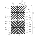
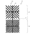
- FIG. 13 is a plan view schematically showing the configuration of one pixel in the liquid crystal display device described in Patent Document 1.
- FIG. 14 shows the electric field distribution in the BB ′ cross section of the pixel shown in FIG. 13
- FIG. 15 shows the luminance distribution of the pixel shown in FIG. 13
- FIG. 16 shows the alignment state of the liquid crystal in the pixel shown in FIG. FIG.
- the pixel 210 of the liquid crystal display device 200 of Patent Document 1 is surrounded by the scanning line 22 and the signal line 23, and the pixel 210 is switched near the intersection of the scanning line 22 and the signal line 23.
- a TFT (Thin Film Transistor) 35 is provided.
- an auxiliary capacitance line 24 extending in parallel with the scanning line 22 is formed at the center of the pixel 210.
- the pixel electrode 230 disposed in the pixel 210 includes a plurality of line portions having two kinds of widths (a wide line portion 230a and a narrow line) extending in the 45 ° -225 ° direction and the 135 ° -315 ° direction. Part 230b).
- the line portions of the upper right region (the right region above the auxiliary capacitance line 24) 210a and the lower left region (the left region below the auxiliary capacitance line 24) 210c of the pixel 210 are all in the 45 ° -225 ° direction.
- the line portions of the upper left region (the left region above the auxiliary capacitance line 24) 210b and the lower right region (the right region below the auxiliary capacitance line 24) 210d are all in the direction of 135 degrees to 315 degrees.
- the plurality of line portions 230a are arranged so as to be sandwiched between the plurality of line portions 230b. Therefore, each of these four regions 210a, 210b, 210c, and 210d includes two boundaries between the wide line portion 230a and the narrow line portion 230b.
- the present invention has been made to solve the above-described problems, and an object of the present invention is to provide a liquid crystal display device having high transmittance and high display quality with excellent gradation and viewing angle characteristics.
- a liquid crystal display device is a vertical alignment type liquid crystal display device having a plurality of pixels, a pair of polarizing plates having transmission axes orthogonal to each other, a first electrode, and a first electrode facing the first electrode.
- Two electrodes and a liquid crystal layer disposed between the first electrode and the second electrode, and each of the plurality of pixels is a straight line parallel or perpendicular to the direction of the transmission axis of the pair of polarizing plates
- a plurality of first branches extending in a first direction in each of the first region and the second region; and A plurality of second branch portions extending in a second direction different from the one direction, each of the plurality of first branch portions in the first region having a first width, and the plurality of the second branch portions in the second region.
- Each of the first branch portions of the first branch portion is different from the first width. Having a second width.
- each of the plurality of second branch portions in the first region has the first width
- each of the plurality of second branch portions in the second region has the second width.
- any two adjacent ones of the plurality of first branch portions in the first region are arranged at a first interval, and the plurality of first branches in the second region are arranged. Any two adjacent ones of the sections are arranged with a second interval different from the first interval.
- any two adjacent ones of the plurality of second branch portions in the first region are arranged with the first interval, and the plurality of second portions in the second region.
- Arbitrary two adjacent ones of the branches are arranged with the second interval.
- the first region and the second region correspond to one region and the other region of the pixels partitioned by a gate bus line or a CS line, respectively.
- the first region and the second region respectively correspond to one region and the other region of the pixels separated by a line parallel to the source bus line.
- the first direction and the second direction are orthogonal to each other, and the direction of the transmission axis of the pair of polarizing plates and the first direction are 45 degrees, 135 degrees, 225 degrees, or 315 degrees. Is different.
- liquid crystal domains having different alignment directions of liquid crystal molecules are formed in each of the first region and the second region.
- each of the plurality of pixels has a third region separated from the first region or the second region by a straight line parallel or perpendicular to the direction of the transmission axis of the pair of polarizing plates
- the first electrode includes the plurality of first branch portions and the plurality of second branch portions in the third region, and the plurality of first branch portions and the plurality of second portions in the third region.
- Each of the branch portions has a third width different from the first width or the second width.
- the tilt angle of the liquid crystal molecules in the first region when no voltage is applied to the liquid crystal layer is different from the tilt angle of the liquid crystal molecules in the second region.
- Another liquid crystal display device is a vertical alignment type liquid crystal display device having a plurality of pixels, a pair of polarizing plates having transmission axes orthogonal to each other, a first electrode, and facing the first electrode. And a liquid crystal layer disposed between the first electrode and the second electrode, wherein each of the plurality of pixels is parallel or perpendicular to a transmission axis direction of the pair of polarizing plates.
- a plurality of first branches extending in the first direction in each of the first region and the second region, the first region and the second region being separated from each other by a straight line;
- a plurality of second branch portions extending in a second direction different from the first direction, and any two adjacent ones of the plurality of first branch portions in the first region are spaced apart from each other by a first interval.
- any two adjacent ones of the plurality of second branch portions in the first region are arranged with the first interval, and the plurality of second portions in the second region.
- Arbitrary two adjacent ones of the branches are arranged with the second interval.
- each of the plurality of pixels has a third region separated from the first region or the second region by a straight line parallel or perpendicular to the direction of the transmission axis of the pair of polarizing plates,
- the first electrode includes the plurality of first branch portions and the plurality of second branch portions in the third region, and is adjacent to any one of the plurality of first branch portions in the third region.
- two adjacent ones of the plurality of second branch portions in the third region are arranged with a third interval different from the first interval or the second interval.
- the tilt angle of the liquid crystal molecules in the first region when no voltage is applied to the liquid crystal layer is different from the tilt angle of the liquid crystal molecules in the second region.
- Another liquid crystal display device is a vertical alignment type liquid crystal display device having a plurality of pixels, a pair of polarizing plates having transmission axes orthogonal to each other, a first electrode, and facing the first electrode. And a liquid crystal layer disposed between the first electrode and the second electrode, wherein each of the plurality of pixels is parallel or perpendicular to a transmission axis direction of the pair of polarizing plates.
- Each of the plurality of regions includes a plurality of first branch portions extending in a first direction, and a second portion different from the first direction.
- a plurality of second branches extending in a direction, each of the plurality of first branches in one of the plurality of regions has a first width, and the other in the other of the plurality of regions.
- Each of the plurality of first branch portions is different from the first width. It has a width.
- each of the plurality of second branch portions in one of the plurality of regions has the first width, and the plurality of second branch portions in the other one of the plurality of regions. Each has the second width.
- Another liquid crystal display device is a vertical alignment type liquid crystal display device having a plurality of pixels, a pair of polarizing plates having transmission axes orthogonal to each other, a first electrode, and facing the first electrode. And a liquid crystal layer disposed between the first electrode and the second electrode, wherein each of the plurality of pixels is parallel or perpendicular to a transmission axis direction of the pair of polarizing plates.
- Each of the plurality of regions includes a plurality of first branch portions extending in a first direction, and a second portion different from the first direction.
- a plurality of second branch portions extending in a direction, and any two adjacent ones of the plurality of first branch portions in one of the plurality of regions are arranged at a first interval, The plurality of first branch portions in the other one of the plurality of regions. Two arbitrary adjacent Chino, but is spaced a second interval different from the first distance.
- any two adjacent ones of the plurality of second branch portions in one of the plurality of regions are arranged with the first interval therebetween, and the other regions of the plurality of regions Arbitrary adjacent two of the plurality of second branch portions in one are arranged with the second interval therebetween.
- the fishbone electrode has a plurality of regions having different branch widths or intervals, and these regions are separated by a straight line parallel or perpendicular to the transmission axis direction of the polarizing plate. Therefore, branches having different widths are not adjacent to each other in the liquid crystal domain. Therefore, according to the liquid crystal display device of the present invention, high-quality display with high luminance and excellent gradation or viewing angle characteristics is possible.
- FIG. 2 is a schematic cross-sectional view of the liquid crystal display device according to Embodiment 1 taken along the line A-A ′ in FIG. 1.
- 3 is a plan view schematically showing the shape of a pixel electrode of the liquid crystal display device of Embodiment 1.
- FIG. 3 is a graph showing VT characteristics by pixels of the liquid crystal display device of Embodiment 1.
- FIG. 4 is a graph for explaining viewing angle characteristics of pixels of the liquid crystal display device of Embodiment 1.
- 3 is a diagram illustrating a state of white display by pixels of the liquid crystal display device of Embodiment 1.
- FIG. 1 is a plan view schematically showing a configuration of one pixel in a liquid crystal display device described in Patent Document 1.
- FIG. 1 is a plan view schematically showing a configuration of one pixel in a liquid crystal display device described in Patent Document 1.
- FIG. 14 is a diagram showing an electric field distribution in the B-B ′ cross section of the pixel shown in FIG. 13. It is a figure showing the luminance distribution of the pixel shown in FIG. It is a figure showing the orientation state of the liquid crystal in the pixel shown in FIG.
- FIG. 1 is a plan view schematically showing the structure of one pixel in the liquid crystal display device 100 of Embodiment 1 according to the present invention.
- FIG. 2 is along the line AA ′ in FIG. It is a typical sectional view.
- the liquid crystal display device 100 is a vertical alignment type liquid crystal display device that has a plurality of pixels 10 having the configuration shown in FIG. 1 and performs display in a normally black mode by the pixels 10 arranged in a matrix. Further, as shown in FIG. 2, the liquid crystal display device 100 includes a TFT substrate 20 that is an active matrix substrate, a counter substrate 40 that is a color filter substrate, and a liquid crystal layer 50 provided between these substrates. ing.
- the liquid crystal layer 50 includes nematic liquid crystal having negative dielectric anisotropy ( ⁇ ⁇ 0).
- a polarizing plate 60 a is provided outside the TFT substrate 20 (opposite the liquid crystal layer 50), and a polarizing plate 60 b is provided outside the counter substrate 40.
- the polarizing plates 60a and 60b are arranged in crossed Nicols, and one light transmission axis thereof extends in the horizontal direction in FIG. 1, and the other light transmission axis extends in the vertical direction.
- the azimuth direction from the left side to the right side in FIG. 1 is defined as the azimuth direction of 0 °, and the azimuth angle is set counterclockwise with reference to this.
- the TFT substrate 20 includes a glass substrate (transparent substrate) 21, scanning lines (gate bus lines) 22 and signal lines (data bus lines) 23 formed on the glass substrate 21. And an auxiliary capacitance line (Cs line) 24, an insulating layer 25 formed on these wirings, and a pixel electrode 30 and an alignment film 26 formed on the insulating layer 25.
- a glass substrate transparent substrate
- scanning lines gate bus lines
- signal lines data bus lines
- Each pixel 10 is surrounded by two adjacent scanning lines 22 and two adjacent signal lines 23, and a TFT 35 for switching a display voltage to the pixel electrode 30 is arranged for each pixel 10.
- the gate electrode and the source electrode of the TFT 35 are electrically connected to the scanning line 22 and the signal line 23, respectively, and the drain electrode is electrically connected to the pixel electrode 30.
- An auxiliary capacitance electrode 36 electrically connected to the auxiliary capacitance line 24 is formed under the pixel electrode 30 in the center of the pixel 10.
- the counter substrate 40 includes a transparent substrate 41, a CF (color filter) layer 42 disposed on the transparent substrate 41 (on the surface on the liquid crystal layer 50 side), and a common electrode 43 formed on the CF layer 42. And an alignment film 44 formed on the common electrode 43.
- Both the alignment film 26 of the TFT substrate 20 and the alignment film 44 of the counter substrate 40 are composed of an alignment layer and an alignment maintaining layer.
- the alignment layer is a vertical alignment film applied on the substrate
- the alignment maintaining layer is a state in which a voltage is applied to the liquid crystal layer 50 after forming a liquid crystal cell with a photopolymerizable monomer previously mixed in a liquid crystal material. It is formed by photopolymerization with.
- a voltage is applied to the liquid crystal layer 50 by the pixel electrode 30 and the common electrode 43, the liquid crystal molecules are aligned by an oblique electric field generated according to the shape of the pixel electrode 30, and light is irradiated in that state to irradiate the monomer. Is polymerized.
- Alignment can be maintained (stored) in the liquid crystal molecules even after the voltage is removed (a state where no voltage is applied) by the alignment maintaining layer formed in this way.
- the alignment films 26 and 44 are formed so as to give a pretilt angle of 2 ° to the liquid crystal in the entire pixel 10.
- the technique for forming such an alignment film is called a polymer aligned alignment (PSA) technique, and details thereof are described in Patent Documents 2 and 3. This specification uses these patent documents, and detailed description of the alignment maintaining layer is omitted here.
- the pixel 10 includes a first region 31 above a virtual boundary line 37 passing through the center of the auxiliary capacitance line 24 and a second region 32 below the boundary line 37. .
- the pixel 10 includes the first region 31 and the second region 32 that are separated from each other by a straight line (boundary line 37) that is parallel or perpendicular to the direction of the transmission axis of the pair of polarizing plates 60a and 60b.
- the first region 31 and the second region 32 may be defined as regions separated from each other by the storage capacitor line 24, and a pixel configuration in which both regions are separated by the scanning line 22 or the signal line 23 may be adopted.
- FIG. 3 is a plan view showing the shape of the pixel electrode 30.
- the pixel electrode 30 includes trunk portions 30a and 30a ′ extending in the direction of azimuth angle 0 ° -180 °, trunk portions 30b and 30b ′ extending in the direction of azimuth angle 90 ° -270 °, and azimuth angle 45 °.
- a plurality of branch portions 30c and 30c ′ (first branch portion) extending in the ⁇ 225 ° direction (first direction) and a plurality of branch portions 30d and 30d ′ extending in the azimuth angle 135 ° to 315 ° direction (second direction). (Second branch).
- the pixel electrode 30 in the first region 31 includes trunk portions 30a and 30b extending perpendicularly to each other through the vicinity of the center of the first region 31, and a plurality of branch portions 30c and a plurality of branch portions extending branched from the trunk portion 30a or 30b. 30d.
- the upper right part also referred to as domain
- the upper left part, the lower left part, and the lower right part of the figure are respectively designated as the first part 31a
- the first portion 31a has a branch portion 30c in the direction of 45 ° from the trunk portion 30a or 30b
- the second portion 31b has a branch portion in the direction of 135 ° from the trunk portion 30a or 30b.
- the branch portion 30d extends in the 225 ° direction from the trunk portion 30a or 30b in the third portion 31c
- the branch portion 30d extends in the 315 ° direction from the trunk portion 30a or 30b in the fourth portion 31d.
- the widths (first widths) L1 of the branch part 30c and the branch part 30d are all the same. Further, the distance between any two branch portions 30c adjacent in each of the first portion 31a and the third portion 31c, and any two branch portions 30d adjacent in each of the second portion 31b and the fourth portion 31d. The distances S1 between are all the same.
- the pixel electrode 30 in the second region 32 includes trunk portions 30a ′ and 30b ′ extending orthogonally to each other through the vicinity of the center of the second region 32, and a plurality of branch portions 30c ′ extending branched from the trunk portion 30a ′ or 30b ′. And a plurality of branch portions 30d ′.
- the upper right portion, the upper left portion, the lower left portion, and the lower right portion of the drawing are respectively represented as a first portion 32a and a second portion.
- the first portion 32a has a branch portion 30c ′ in the direction of 45 ° from the trunk portion 30a ′ or 30b ′
- the second portion 32b has a trunk portion 30a ′ or 30b ′ to 135 °.
- the branch part 30c 'and the branch part 30d' all have the same width (second width) L2 different from the width L1. Further, the distance between any two branch portions 30c ′ adjacent to each other in each of the first portion 32a and the third portion 32c, and any two branch portions adjacent to each other in each of the second portion 32b and the fourth portion 32d. The distances S2 between 30d ′ are all the same. The distance S2 is different from the distance S1.
- the branch widths L1 and L2 mean the width in the direction perpendicular to the extending direction of the branch parts, and the distances S1 and S2 between the two branch parts are formed between two adjacent branch parts. It means the width in the direction perpendicular to the direction in which the branch part of the gap (slit part) extends.
- the widths L1 and L2 may be referred to as line widths L1 and L2, respectively, and the distances S1 and S2 may be referred to as slit widths S1 and S2, respectively.
- the values of the width L1 and the distance S1 are, for example, 1.5 ⁇ m and 3.0 ⁇ m, respectively, and the values of the width L2 and the distance S2 are, for example, 2.5 ⁇ m and 2.5 ⁇ m, respectively. Although it is not necessary to limit the widths L1 and L2 and the distances S1 and S2 to these values, it is desirable to set these values to values of 5.0 ⁇ m or less.
- a multi-domain having a 4D structure is formed in each of the first region 31 and the second region 32 by the pixel electrode 30 and the alignment films 26 and 44 having the above-described shape.
- the pretilt orientation of the liquid crystal molecules in each domain has an orientation parallel to the branches 30c, 30d, 30c ′, or 30d ′ in each domain. Show.
- the liquid crystal molecules in each domain are oriented in the direction parallel to the branches 30c, 30d, 30c ′, or 30d ′ in the domain (director direction of the domain) and parallel to the substrate surface. Oriented to At this time, since the orientation azimuth coincides with the pretilt azimuth, orientation in an accurate azimuth with an extremely fast response speed is realized.
- the liquid crystal display device 100 includes the pixel electrode 30 having the above-described shape, the domain formed by the branch portions 30c and 30d of the first region 31 and the branch portions 30c ′ and 30d ′ of the second region.
- the boundary formed with the domain is formed on the boundary line 37 (or the auxiliary capacitance line 24), and there is no region where the wide branch part and the narrow branch part are adjacent to each other in each domain.
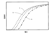
- FIG. 4 is a diagram showing the voltage dependency (referred to as VT characteristics) of the transmittance obtained from the first region 31 and the second region 32 when the display surface is viewed from the front (polar angle 0 ° direction). .
- Lines a and b in the figure indicate VT characteristics in the first region 31 and the second region 32, respectively.
- the width of the branch portion or the interval between the two branch portions is different, so that there is a difference in the liquid crystal alignment regulating force in these two regions. Therefore, different VT characteristics as shown in FIG. 4 are obtained from the two regions.
- the VT characteristic of the entire display surface is a characteristic obtained by averaging these two VT characteristics.
- the VT characteristic obtained from a pixel electrode having a specific shape is different from an ideal characteristic, problems such as white floating or dark sinking may appear in the display.
- the liquid crystal display device of Embodiment 1 two different VT characteristics can be obtained from one pixel, and a characteristic obtained by averaging the two VT characteristics can be obtained on the entire display surface. Therefore, ideal brightness and gradation characteristics can be obtained by appropriately setting the widths L1 and L2 and the distances S1 and S2 according to the size, shape, or application of the liquid crystal display device.
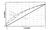
- FIG. 5 is a diagram for explaining the viewing angle characteristics of the liquid crystal display device 100 according to the present embodiment.
- a line m in FIG. 5 indicates the transmittance (front transmittance) when the display surface of the liquid crystal display device 100 having the pixels 10 is viewed from the front, and the display surface viewed from the azimuth angle 45 ° direction and the polar angle 60 ° direction.
- the relationship hereinafter simply referred to as viewing angle characteristics
- the transmittance oblique transmittance
- the line m represents the viewing angle characteristic obtained by averaging the viewing angle characteristics obtained from each of the first region 31 and the second region 32.
- a line n represents a viewing angle characteristic obtained from the first region 31 (the pixel electrode does not have two types of line widths or slit widths). Note that a line l in FIG. 5 is a reference line indicating that the front transmittance and the oblique transmittance are the same.
- FIG. 6 is a diagram showing a white display state in the first area 31 and the second area 32.
- the conventional liquid crystal display device there are two regions (eight in a pixel) in which each of the four domains is adjacent to the wide branch portion and the narrow branch portion.
- the eight domains in the pixel 10 include a region where a wide branch portion and a narrow branch portion are adjacent to each other. do not do. Therefore, according to the first embodiment, abnormal alignment of the liquid crystal hardly occurs, and a display with high luminance in which generation of a dark portion is suppressed as shown in FIG. 6 is possible.
- the shape of the pixel electrode 30 of Embodiment 1 may be the shape of the counter electrode in one pixel, and the same effect as described above can be obtained.
- the liquid crystal display device of the second embodiment is obtained by replacing the pixel electrode 30 of the liquid crystal display device of the first embodiment with another fishbone-shaped pixel electrode, and the other configuration is the same as that of the first embodiment. . Therefore, only the pixel electrode will be described below.
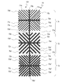
- FIG. 7 is a plan view schematically showing one of the plurality of pixel electrodes 70 arranged in the liquid crystal display device 101 of the second embodiment.
- the pixel electrode 70 includes trunk portions 70a, 70a ′ and 70a ′′ extending in the direction of azimuth angle 0 ° -180 °, and trunk portions 70b, 70b ′ extending in the direction of azimuth angle 90 ° -270 °, and 70b ′′, a plurality of branches 70c, 70c ′ and 70c ′′ (first branch) extending in the azimuth 45 ° -225 ° direction (first direction), and the azimuth 135 ° -315 ° direction (second A plurality of branch portions 70d, 70d ′ and 70d ′′ (second branch portion) extending in the direction).
- the pixel according to the second embodiment includes a first region 71, a first region 71, and a first region 71, which are separated from each other by two virtual boundary lines 77 a and 77 b that extend parallel to the scanning line (parallel or perpendicular to the direction of the transmission axis of the pair of polarizing plates).
- the boundary line 77a partitions the first region 71 and the second region 72 from each other, and the boundary line 77b partitions the second region 72 and the third region 73 from each other.
- the pixel electrode 70 in the first region 71 includes trunk portions 70a and 70b extending perpendicularly to each other through the vicinity of the center of the first region 71, and a plurality of branch portions 70c and a plurality of branch portions extending branched from the trunk portion 70a or 70b. 70d.
- the upper right portion also referred to as a domain
- the upper left portion, the lower left portion, and the lower right portion of the figure are respectively referred to as the first portion 71a and the first portion 71a.
- the first portion 71a has a branch portion 70c in the 45 ° direction from the trunk portion 70a or 70b
- the second portion 71b has the branch portion 70c in the 135 ° direction from the trunk portion 70a or 70b.
- the branch portion 70d extends in the 225 ° direction from the trunk portion 70a or 70b in the third portion 71c
- the branch portion 70d extends in the 315 ° direction from the trunk portion 70a or 70b in the fourth portion 71d.
- the branch portions 70c and 70d have the same width (first line width). Further, the distance between any two branch portions 70c adjacent in each of the first portion 71a and the third portion 71c, and any two branch portions 70d adjacent in each of the second portion 71b and the fourth portion 71d. The distance between them (the first slit width) is the same.
- the pixel electrodes in the second region 72 include trunk portions 70a ′ and 70b ′ that extend orthogonally to each other through the vicinity of the center of the second region 72, and a plurality of branch portions 70c ′ that extend from the trunk portions 70a ′ or 70b ′. It consists of a plurality of branch portions 70d '.
- the upper right portion, the upper left portion, the lower left portion, and the lower right portion of the drawing are respectively referred to as the first portion 72a and the second portion.
- the first portion 72a has a branch portion 70c ′ in the direction of 45 ° from the trunk portion 70a ′ or 70b ′
- the second portion 72b has a branch portion 70c ′ or 70b ′ to 135d.
- the branch part 70c 'and the branch part 70d' all have the same width (second line width) different from the first line width. Further, the distance between any two branch portions 70c ′ adjacent to each other in each of the first portion 72a and the third portion 72c, and any two branch portions adjacent to each other in each of the second portion 72b and the fourth portion 72d. All the distances (second slit widths) between 70d 'are the same. The second slit width is different from the first slit width.
- the pixel electrodes in the third region 73 include trunk portions 70a ′′ and 70b ′′ extending perpendicularly to each other through the vicinity of the center of the third region 73, and a plurality of branch portions 70c ′′ extending from the trunk portions 70a ′′ or 70b ′′. It consists of a plurality of branch portions 70d ′′.
- the upper right portion, the upper left portion, the lower left portion, and the lower right portion of the drawing are respectively represented as a first portion 73a and a second portion.
- the first portion 73a has a branch portion 70c ′′ in the 45 ° direction from the trunk portion 70a ′′ or 70b ′′
- the second portion 73b has a trunk portion 70a ′′ or 70b ′′.
- the branch portion 70d ′′ extends in the direction of °
- the branch portion 70c ′′ extends from the trunk portion 70a ′′ or 70b ′′ to the 225 ° direction in the third portion 73c
- the branch portion 70d extends in the direction of 315 ° from the trunk portion 70a ′′ or 70b ′′ in the fourth portion 73d. "Is extended respectively.
- the branch part 70c "and the branch part 70d" all have the same width (third line width) different from the first line width or the second line width. Further, the distance between any two branch portions 70c ′′ adjacent in each of the first portion 73a and the third portion 73c, and any two branch portions adjacent in each of the second portion 73b and the fourth portion 73d. The distance between 70d ′′ (the third slit width) is the same. The third slit width is different from the first slit width or the second slit width.
- the first line width, the second line width, and the third line width are, for example, 1.5 ⁇ m, 2.5 ⁇ m, and 2.0 ⁇ m, respectively, and the first slit width, the second slit width, and The third slit width is, for example, 4.0 ⁇ m, 3.5 ⁇ m, and 2.5 ⁇ m, respectively. Although it is not necessary to limit the line width and the slit width to these values, it is desirable to set these values to values of 5.0 ⁇ m or less.
- a multi-domain having a 4D structure is formed in each of the first region 71, the second region 72, and the third region 73 by the pixel electrode 70 having the above-described shape and the alignment film.
- the pretilt orientation of the liquid crystal molecules in each domain shows an orientation parallel to the branches in each domain.
- the liquid crystal molecules in each domain are oriented in a polar angle direction that is parallel to the branches in the domain (director direction of the domain) and approaches parallel to the substrate surface.
- the orientation azimuth coincides with the pretilt azimuth, orientation in an accurate azimuth with an extremely fast response speed is realized.
- the liquid crystal display device 101 includes the pixel electrode 70 having the above-described shape, the domain formed by the branch portions 70c and 70d of the first region 71 and the branch portions 70c ′ and 70d of the second region 72 are used.
- the boundary between the domain formed by ' is formed on the boundary line 77a, and is formed by the domain formed by the branches 70c' and 70d 'of the second region 72 and the branches 70c "and 70d" of the third region 73.
- the boundary with the domain to be formed is formed on the boundary line 77b. Therefore, there is no region where branches having different widths are adjacent to each other in each domain.
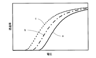
- FIG. 8 shows voltage dependency (VT characteristics) of transmittance obtained from the first region 71, the second region 72, and the third region 73 when the display surface is viewed from the front (polar angle 0 ° direction).
- FIG. Lines a, b, and c in FIG. 8 indicate VT characteristics in the first region 71, the second region 72, and the third region 73, respectively.
- the width of the branch portion or the interval between the two branch portions is different, so that there is a difference in the liquid crystal alignment regulating force in these three regions. Therefore, different VT characteristics as shown in FIG. 8 are obtained from the three regions.
- the VT characteristic of the entire display surface is a characteristic obtained by averaging these three VT characteristics.
- the liquid crystal display device of the second embodiment three different VT characteristics can be obtained from one pixel, and a characteristic obtained by averaging the three VT characteristics can be obtained on the entire display surface. Accordingly, it is possible to obtain ideal luminance and gradation characteristics by appropriately setting the line width and slit width in each region according to the size, shape, or application of the liquid crystal display device.
- FIG. 9 is a diagram for explaining the viewing angle characteristics of the liquid crystal display device 101 according to the second embodiment.
- a line m in FIG. 9 represents the viewing angle characteristic of the liquid crystal display device 101 of the present embodiment having the pixel electrode 70. That is, the line m represents the viewing angle characteristic obtained by averaging the viewing angle characteristics obtained from the first area 71, the second area 72, and the third area 73, respectively.
- the line n indicates the average viewing angle characteristics of two of the first area 71, the second area 72, and the third area 73 (for example, the average viewing angle characteristics of the first area 71 and the third area 73).
- the line o represents the viewing angle characteristic of one of the first region 71, the second region 72, and the third region 73 (for example, the first region 71).
- a line l in FIG. 9 is a reference line indicating that the front transmittance and the oblique transmittance are the same.
- a viewing angle characteristic superior to that of a liquid crystal display device using a pixel electrode having a single line width and slit width can be obtained.
- a viewing angle characteristic superior to a liquid crystal display device using a pixel electrode having a line width and a slit width can be obtained.
- the shape of the pixel electrode 70 of Embodiment 2 may be the shape of the counter electrode in one pixel, and the same effect as described above can be obtained.
- Embodiment 3 a liquid crystal display device according to Embodiment 3 of the present invention will be described.
- the liquid crystal display device of the third embodiment is obtained by changing the pretilt angle of the liquid crystal obtained by the alignment films 26 and 44 of the liquid crystal display device of the first embodiment to other angles, and other configurations are the same as those of the first embodiment. Is the same. In the following, description will be made with a focus on differences from the first embodiment.
- FIG. 10 is a plan view schematically showing the configuration of the pixel 10 ′ in the liquid crystal display device 102 according to the third embodiment.
- the pixel 10 ′ includes a first region 31 ′ and a second region 32 ′ separated from each other by a boundary line 37, and has the pixel electrode 30 having the shape described in the first embodiment.
- the tilt angle of the liquid crystal molecules in the first region 31 ′ when no voltage is applied to the liquid crystal layer is different from the tilt angle of the liquid crystal molecules in the second region 32 ′.
- the alignment films 26 and 44 in the first region 31 ′ are formed so as to give a pretilt angle of 2 ° to the liquid crystal, and the alignment films 26 and 44 in the second region 32 ′ give a pretilt angle of 5 ° to the liquid crystal. Is formed.
- FIG. 11 is a diagram showing the VT characteristics of the first region 31 ′ and the second region 32 ′ when the display surface is viewed from the front (polar angle 0 ° direction).
- Lines a and c in the figure indicate VT characteristics of the first region 31 ′ and the second region 32 ′, respectively, and a line b indicates VT characteristics of the second region 32 of the first embodiment.
- the VT characteristics in both regions are the same, but from the VT characteristics indicated by the lines c and b, the second It can be seen that the transmittance in the region 32 ′ is higher than the transmittance in the second region 32 of the first embodiment.
- the first region 31 ′ and the second region 32 ′ are different in pretilt angle, so that the luminance difference between the two regions is larger than that in the first embodiment.
- FIG. 12 is a diagram for explaining the viewing angle characteristics of the liquid crystal display device 102 according to the present embodiment.
- a line o in FIG. 12 represents the viewing angle characteristic of the pixel 10 ′ of the third embodiment. That is, the line o represents the average viewing angle characteristic obtained from each of the first region 31 'and the second region 32' described above.
- the line m represents the viewing angle characteristic of the pixel 10 of the first embodiment, that is, the viewing angle characteristic of the pixel having the pixel electrode 30 but not causing a different pretilt angle
- the line n represents the first region 31 ′.
- a viewing angle characteristic in one of the second regions 32 ′ here, the first region 31 ′.
- a line l in FIG. 12 is a reference line indicating that the front transmittance and the oblique transmittance are the same.
- the same pixel as in the first embodiment is used, and a plurality of pretilt angles are generated in the pixel, so that a liquid crystal display device using a pixel electrode having a single line width and slit width can be obtained.
- a viewing angle characteristic better than that of the liquid crystal display device according to the first embodiment in which all the pretilt angles in the pixels are the same can be obtained.
- the pretilt angle is changed according to the difference in the line width or slit width of the pixel electrode 30, display with higher luminance and better viewing angle characteristics than in the first embodiment is possible. . Further, from the comparison between the first and third embodiments, by changing the pretilt angle in accordance with the difference in the line width or slit width of the pixel electrode 30, the viewing angle characteristics of the entire display surface are improved and the luminance in the entire display surface is increased. It can be seen that can be adjusted to a wider range.
- the present invention is used for a liquid crystal display device having a relatively small pixel pitch, such as a liquid crystal display device for a cellular phone.
Abstract
Description
20 TFT基板
21 ガラス基板
22 走査線
23 信号線
24 補助容量線
25 絶縁層
26 配向膜
30 画素電極
30a、30a’、30b、30b’ 幹部
30c、30c’、30d、30d’ 枝部
31、31’ 第1領域
32、32’ 第2領域
35 TFT
36 補助容量電極
37 境界線
40 対向基板
41 透明基板
42 CF層
43 共通電極
44 配向膜
50 液晶層
60a、60b 偏光板
70 画素電極
70a、70a’70a”、70b、70b’、70b” 幹部
70c、70c’、70c”、70d、70d’、70d”、 枝部
71 第1領域
72 第2領域
73 第3領域
77a、77b 境界線
100、101、102 液晶表示装置 10
36
図1は、本発明による実施形態1の液晶表示装置100における1つの画素の構造を模式的に示す平面図であり、図2は、液晶表示装置100の図1におけるA-A’線に沿った模式的な断面図である。 (Embodiment 1)
FIG. 1 is a plan view schematically showing the structure of one pixel in the liquid
以下、本発明による実施形態2の液晶表示装置を説明する。実施形態2の液晶表示装置は、実施形態1の液晶表示装置の画素電極30を他のフィッシュボーン形状の画素電極に置き換えたものであり、それ以外の構成は実施形態1のものと同じである。よって以下、画素電極についてのみ説明を行うものとする。 (Embodiment 2)
Hereinafter, a liquid crystal display device according to a second embodiment of the present invention will be described. The liquid crystal display device of the second embodiment is obtained by replacing the
以下、本発明による実施形態3の液晶表示装置を説明する。実施形態3の液晶表示装置は、実施形態1の液晶表示装置の配向膜26及び44によって得られる液晶のプレチルト角を他の角度に変えたものであり、それ以外の構成は実施形態1のものと同じである。以下、実施形態1と異なる部分を中心に説明を行う。 (Embodiment 3)
Hereinafter, a liquid crystal display device according to Embodiment 3 of the present invention will be described. The liquid crystal display device of the third embodiment is obtained by changing the pretilt angle of the liquid crystal obtained by the
Claims (18)
- 複数の画素を有する垂直配向型の液晶表示装置であって、
互いに直交する透過軸を有する一対の偏光板と、
第1電極と、
前記第1電極に対向する第2電極と、
前記第1電極と前記第2電極との間に配置された液晶層と、を備え、
前記複数の画素のそれぞれが、前記一対の偏光板の透過軸の方向に平行または垂直な直線によって互いに区分された第1領域および第2領域を有し、
前記第1電極が、前記第1領域および前記第2領域のそれぞれにおいて、第1方向に延びる複数の第1枝部と、前記第1方向とは異なる第2方向に延びる複数の第2枝部とを備え、
前記第1領域における前記複数の第1枝部のそれぞれが第1の幅を有し、
前記第2領域における前記複数の第1枝部のそれぞれが前記第1の幅とは異なる第2の幅を有する、液晶表示装置。 A vertical alignment type liquid crystal display device having a plurality of pixels,
A pair of polarizing plates having transmission axes orthogonal to each other;
A first electrode;
A second electrode facing the first electrode;
A liquid crystal layer disposed between the first electrode and the second electrode,
Each of the plurality of pixels has a first region and a second region separated from each other by a straight line parallel or perpendicular to the direction of the transmission axis of the pair of polarizing plates,
In each of the first region and the second region, the first electrode includes a plurality of first branch portions extending in a first direction, and a plurality of second branch portions extending in a second direction different from the first direction. And
Each of the plurality of first branches in the first region has a first width;
The liquid crystal display device, wherein each of the plurality of first branch portions in the second region has a second width different from the first width. - 前記第1領域における前記複数の第2枝部のそれぞれが前記第1の幅を有し、
前記第2領域における前記複数の第2枝部のそれぞれが前記第2の幅を有する、請求項1に記載の液晶表示装置。 Each of the plurality of second branches in the first region has the first width;
The liquid crystal display device according to claim 1, wherein each of the plurality of second branch portions in the second region has the second width. - 前記第1領域における前記複数の第1枝部のうちの任意の隣り合う2つが、第1の間隔を空けて配置されており、
前記第2領域における前記複数の第1枝部のうちの任意の隣り合う2つが、前記第1の間隔とは異なる第2の間隔を空けて配置されている、請求項1または2に記載の液晶表示装置。 Any two adjacent ones of the plurality of first branches in the first region are arranged at a first interval;
The arbitrary adjacent two of the plurality of first branch portions in the second region are arranged with a second interval different from the first interval. Liquid crystal display device. - 前記第1領域における前記複数の第2枝部のうちの任意の隣り合う2つが、前記第1の間隔を空けて配置されており、
前記第2領域における前記複数の第2枝部のうちの任意の隣り合う2つが、前記第2の間隔を空けて配置されている、請求項3に記載の液晶表示装置。 Arbitrary adjacent two of the plurality of second branch portions in the first region are arranged with the first interval,
4. The liquid crystal display device according to claim 3, wherein any two adjacent ones of the plurality of second branch portions in the second region are arranged with the second interval. - 前記第1領域および前記第2領域が、それぞれ、ゲートバスラインまたはCSラインによって区切られた画素の一方の領域および他方の領域に相当する、請求項1から4のいずれか1項に記載の液晶表示装置。 5. The liquid crystal according to claim 1, wherein the first region and the second region correspond to one region and the other region of a pixel partitioned by a gate bus line or a CS line, respectively. Display device.
- 前記第1領域および前記第2領域が、それぞれ、ソースバスラインに平行な線によって区切られた画素の一方の領域および他方の領域に相当する、請求項1から4のいずれか1項に記載の液晶表示装置。 The said 1st area | region and the said 2nd area | region correspond to one area | region and the other area | region of the pixel each divided | segmented by the line parallel to a source bus line, respectively. Liquid crystal display device.
- 前記第1方向と前記第2方向が直交しており、
前記一対の偏光板の透過軸の方向と前記第1方向とが、45度、135度、225度、又は315度異なっている、請求項1から6のいずれか1項に記載の液晶表示装置。 The first direction and the second direction are orthogonal to each other;
The liquid crystal display device according to any one of claims 1 to 6, wherein a direction of a transmission axis of the pair of polarizing plates and the first direction are different by 45 degrees, 135 degrees, 225 degrees, or 315 degrees. . - 前記液晶層に電圧が印加されたとき、前記第1領域および前記第2領域のそれぞれにおいて、液晶分子の配向方向が互いに異なる4つの液晶ドメインが形成される、請求項1から7のいずれか1項に記載の液晶表示装置。 8. The liquid crystal domain according to claim 1, wherein when a voltage is applied to the liquid crystal layer, four liquid crystal domains having different alignment directions of liquid crystal molecules are formed in each of the first region and the second region. The liquid crystal display device according to item.
- 前記複数の画素のそれぞれが、前記一対の偏光板の透過軸の方向に平行または垂直な直線によって前記第1領域または前記第2領域と区分された第3領域を有し、
前記第1電極が前記第3領域の中に、前記複数の第1枝部と前記複数の第2枝部とを備え、
前記第3領域における前記複数の第1枝部および前記複数の第2枝部のそれぞれが、前記第1の幅または前記第2の幅と異なる第3の幅を有する、請求項1から8のいずれか1項に記載の液晶表示装置。 Each of the plurality of pixels has a third region separated from the first region or the second region by a straight line parallel or perpendicular to the direction of the transmission axis of the pair of polarizing plates,
The first electrode includes the plurality of first branch portions and the plurality of second branch portions in the third region,
9. The device according to claim 1, wherein each of the plurality of first branch portions and the plurality of second branch portions in the third region has a third width different from the first width or the second width. The liquid crystal display device according to any one of the above. - 前記液晶層に電圧が印加されていない場合の前記第1領域における液晶分子の傾斜角度が前記第2領域における液晶分子の傾斜角度と異なる、請求項1から9のいずれか1項に記載の液晶表示装置。 10. The liquid crystal according to claim 1, wherein an inclination angle of liquid crystal molecules in the first region when no voltage is applied to the liquid crystal layer is different from an inclination angle of liquid crystal molecules in the second region. Display device.
- 複数の画素を有する垂直配向型の液晶表示装置であって、
互いに直交する透過軸を有する一対の偏光板と、
第1電極と、
前記第1電極に対向する第2電極と、
前記第1電極と前記第2電極との間に配置された液晶層と、を備え、
前記複数の画素のそれぞれが、前記一対の偏光板の透過軸の方向に平行または垂直な直線によって互いに区分された第1領域および第2領域を有し、
前記第1電極が、前記第1領域および前記第2領域のそれぞれにおいて、第1方向に延びる複数の第1枝部と、前記第1方向とは異なる第2方向に延びる複数の第2枝部とを備え、
前記第1領域における前記複数の第1枝部のうちの任意の隣り合う2つが、第1の間隔を空けて配置されており、
前記第2領域における前記複数の第1枝部のうちの任意の隣り合う2つが、前記第1の間隔とは異なる第2の間隔を空けて配置されている、液晶表示装置。 A vertical alignment type liquid crystal display device having a plurality of pixels,
A pair of polarizing plates having transmission axes orthogonal to each other;
A first electrode;
A second electrode facing the first electrode;
A liquid crystal layer disposed between the first electrode and the second electrode,
Each of the plurality of pixels has a first region and a second region separated from each other by a straight line parallel or perpendicular to the direction of the transmission axis of the pair of polarizing plates,
In each of the first region and the second region, the first electrode includes a plurality of first branch portions extending in a first direction, and a plurality of second branch portions extending in a second direction different from the first direction. And
Any two adjacent ones of the plurality of first branches in the first region are arranged at a first interval;
The liquid crystal display device, wherein any two adjacent ones of the plurality of first branch portions in the second region are arranged with a second interval different from the first interval. - 前記第1領域における前記複数の第2枝部のうちの任意の隣り合う2つが、前記第1の間隔を空けて配置されており、
前記第2領域における前記複数の第2枝部のうちの任意の隣り合う2つが、前記第2の間隔を空けて配置されている、請求項11に記載の液晶表示装置。 Arbitrary adjacent two of the plurality of second branch portions in the first region are arranged with the first interval,
The liquid crystal display device according to claim 11, wherein any two adjacent two of the plurality of second branch portions in the second region are arranged with the second space therebetween. - 前記複数の画素のそれぞれが、前記一対の偏光板の透過軸の方向に平行または垂直な直線によって前記第1領域または前記第2領域と区分された第3領域を有し、
前記第1電極が前記第3領域の中に、前記複数の第1枝部と前記複数の第2枝部とを備え、
前記第3領域における前記複数の第1枝部のうちの任意の隣り合う2つ、及び前記第3領域における前記複数の第2枝部のうちの任意の隣り合う2つが、前記第1の間隔または前記第2の間隔と異なる第3の間隔を空けて配置されている、請求項11または12に記載の液晶表示装置。 Each of the plurality of pixels has a third region separated from the first region or the second region by a straight line parallel or perpendicular to the direction of the transmission axis of the pair of polarizing plates,
The first electrode includes the plurality of first branch portions and the plurality of second branch portions in the third region,
Any two adjacent ones of the plurality of first branch portions in the third region and any two adjacent ones of the plurality of second branch portions in the third region are the first interval. The liquid crystal display device according to claim 11, wherein the liquid crystal display device is disposed with a third interval different from the second interval. - 前記液晶層に電圧が印加されていない場合の前記第1領域における液晶分子の傾斜角度が前記第2領域における液晶分子の傾斜角度と異なる、請求項11から13のいずれか1項に記載の液晶表示装置。 14. The liquid crystal according to claim 11, wherein an inclination angle of liquid crystal molecules in the first region when no voltage is applied to the liquid crystal layer is different from an inclination angle of liquid crystal molecules in the second region. Display device.
- 複数の画素を有する垂直配向型の液晶表示装置であって、
互いに直交する透過軸を有する一対の偏光板と、
第1電極と、
前記第1電極に対向する第2電極と、
前記第1電極と前記第2電極との間に配置された液晶層と、を備え、
前記複数の画素のそれぞれが、前記一対の偏光板の透過軸の方向に平行または垂直な直線によって互いに区分された複数の領域を有し、
前記第1電極が、前記複数の領域のそれぞれにおいて、第1方向に延びる複数の第1枝部と、前記第1方向とは異なる第2方向に延びる複数の第2枝部とを備え、
前記複数の領域の1つにおける前記複数の第1枝部のそれぞれが第1の幅を有し、
前記複数の領域の他の1つにおける前記複数の第1枝部のそれぞれが前記第1の幅とは異なる第2の幅を有する、液晶表示装置。 A vertical alignment type liquid crystal display device having a plurality of pixels,
A pair of polarizing plates having transmission axes orthogonal to each other;
A first electrode;
A second electrode facing the first electrode;
A liquid crystal layer disposed between the first electrode and the second electrode,
Each of the plurality of pixels has a plurality of regions separated from each other by straight lines parallel or perpendicular to the direction of the transmission axis of the pair of polarizing plates
The first electrode includes a plurality of first branch portions extending in a first direction and a plurality of second branch portions extending in a second direction different from the first direction in each of the plurality of regions.
Each of the plurality of first branches in one of the plurality of regions has a first width;
The liquid crystal display device, wherein each of the plurality of first branch portions in the other one of the plurality of regions has a second width different from the first width. - 前記複数の領域の1つにおける前記複数の第2枝部のそれぞれが前記第1の幅を有し、
前記複数の領域の他の1つにおける前記複数の第2枝部のそれぞれが前記第2の幅を有する、請求項15に記載の液晶表示装置。 Each of the plurality of second branches in one of the plurality of regions has the first width;
The liquid crystal display device according to claim 15, wherein each of the plurality of second branch portions in the other one of the plurality of regions has the second width. - 複数の画素を有する垂直配向型の液晶表示装置であって、
互いに直交する透過軸を有する一対の偏光板と、
第1電極と、
前記第1電極に対向する第2電極と、
前記第1電極と前記第2電極との間に配置された液晶層と、を備え、
前記複数の画素のそれぞれが、前記一対の偏光板の透過軸の方向に平行または垂直な直線によって互いに区分された複数の領域を有し、
前記第1電極が、前記複数の領域のそれぞれにおいて、第1方向に延びる複数の第1枝部と、前記第1方向とは異なる第2方向に延びる複数の第2枝部とを備え、
前記複数の領域の1つにおける前記複数の第1枝部のうちの任意の隣り合う2つが、第1の間隔を空けて配置されており、
前記複数の領域の他の1つにおける前記複数の第1枝部のうちの任意の隣り合う2つが、前記第1の間隔とは異なる第2の間隔を空けて配置されている、液晶表示装置。 A vertical alignment type liquid crystal display device having a plurality of pixels,
A pair of polarizing plates having transmission axes orthogonal to each other;
A first electrode;
A second electrode facing the first electrode;
A liquid crystal layer disposed between the first electrode and the second electrode,
Each of the plurality of pixels has a plurality of regions separated from each other by straight lines parallel or perpendicular to the direction of the transmission axis of the pair of polarizing plates
The first electrode includes a plurality of first branch portions extending in a first direction and a plurality of second branch portions extending in a second direction different from the first direction in each of the plurality of regions.
Arbitrary adjacent two of the plurality of first branch portions in one of the plurality of regions are arranged with a first interval,
Any two adjacent ones of the plurality of first branch portions in the other one of the plurality of regions are disposed with a second interval different from the first interval. . - 前記複数の領域の1つにおける前記複数の第2枝部のうちの任意の隣り合う2つが、前記第1の間隔を空けて配置されており、
前記複数の領域の他の1つにおける前記複数の第2枝部のうちの任意の隣り合う2つが、前記第2の間隔を空けて配置されている、請求項17に記載の液晶表示装置。 Arbitrary adjacent two of the plurality of second branch portions in one of the plurality of regions are arranged with the first interval,
18. The liquid crystal display device according to claim 17, wherein any two adjacent two of the plurality of second branch portions in the other one of the plurality of regions are arranged with the second interval therebetween.
Priority Applications (4)
| Application Number | Priority Date | Filing Date | Title |
|---|---|---|---|
| JP2009552338A JPWO2009098747A1 (en) | 2008-02-04 | 2008-12-25 | Liquid crystal display device |
| CN2008801262146A CN101939696B (en) | 2008-02-04 | 2008-12-25 | Liquid crystal display device |
| US12/866,095 US8345199B2 (en) | 2008-02-04 | 2008-12-25 | Liquid crystal display device |
| EP08872256A EP2246733B1 (en) | 2008-02-04 | 2008-12-25 | Liquid crystal display device |
Applications Claiming Priority (2)
| Application Number | Priority Date | Filing Date | Title |
|---|---|---|---|
| JP2008-024200 | 2008-02-04 | ||
| JP2008024200 | 2008-02-04 |
Publications (1)
| Publication Number | Publication Date |
|---|---|
| WO2009098747A1 true WO2009098747A1 (en) | 2009-08-13 |
Family
ID=40951835
Family Applications (1)
| Application Number | Title | Priority Date | Filing Date |
|---|---|---|---|
| PCT/JP2008/003975 WO2009098747A1 (en) | 2008-02-04 | 2008-12-25 | Liquid crystal display device |
Country Status (5)
| Country | Link |
|---|---|
| US (1) | US8345199B2 (en) |
| EP (1) | EP2246733B1 (en) |
| JP (1) | JPWO2009098747A1 (en) |
| CN (1) | CN101939696B (en) |
| WO (1) | WO2009098747A1 (en) |
Cited By (5)
| Publication number | Priority date | Publication date | Assignee | Title |
|---|---|---|---|---|
| EP2375279A3 (en) * | 2010-04-02 | 2011-12-28 | Samsung Electronics Co., Ltd. | Liquid crystal display panel |
| CN102667595A (en) * | 2009-11-13 | 2012-09-12 | 夏普株式会社 | Liquid crystal display device |
| CN105842938A (en) * | 2010-04-02 | 2016-08-10 | 三星显示有限公司 | Liquid crystal display panel |
| JP2018506739A (en) * | 2015-01-21 | 2018-03-08 | 深▲せん▼市華星光電技術有限公司Shenzhen China Star Optoelectronics Technology Co., Ltd. | Liquid crystal display panel and device |
| TWI683161B (en) * | 2018-08-07 | 2020-01-21 | 友達光電股份有限公司 | Pixel structure |
Families Citing this family (22)
| Publication number | Priority date | Publication date | Assignee | Title |
|---|---|---|---|---|
| WO2009084162A1 (en) * | 2007-12-28 | 2009-07-09 | Sharp Kabushiki Kaisha | Liquid crystal display device |
| US8860913B2 (en) * | 2009-04-08 | 2014-10-14 | Sharp Kabushiki Kaisha | Liquid crystal display device, method for manufacturing liquid crystal display device, composition for forming photopolymer film, and composition for forming liquid crystal layer |
| TWI485495B (en) * | 2011-01-26 | 2015-05-21 | Innolux Corp | Liquid crystal display device |
| CN102305983A (en) * | 2011-08-29 | 2012-01-04 | 深圳市华星光电技术有限公司 | Liquid crystal display panel and display device using liquid crystal display panel |
| US20130050629A1 (en) * | 2011-08-29 | 2013-02-28 | Shenzhen China Star Optoelectronics Technology Co., Ltd. | Liquid crystal display panel and display apparatus using the same |
| CN103513472A (en) * | 2012-06-26 | 2014-01-15 | 群康科技(深圳)有限公司 | Substrate, display device provided with substrate and manufacturing method of display device |
| CN102768443B (en) * | 2012-07-09 | 2015-06-17 | 深圳市华星光电技术有限公司 | Liquid crystal display panel and display device applied thereby |
| US8830431B2 (en) * | 2012-07-16 | 2014-09-09 | Shenzhen China Star Optoelectronics Technology Co., Ltd | Pixel electrode and LCD device |
| US10712596B2 (en) * | 2013-08-02 | 2020-07-14 | Samsung Display Co., Ltd. | Liquid crystal display |
| CN103454816B (en) * | 2013-08-09 | 2016-03-30 | 深圳市华星光电技术有限公司 | A kind of display panels |
| KR102078810B1 (en) | 2013-08-14 | 2020-02-20 | 삼성디스플레이 주식회사 | Liquid crystal display |
| CN103792741B (en) | 2014-01-23 | 2016-06-22 | 京东方科技集团股份有限公司 | A kind of array base palte and preparation method thereof, display device |
| TWI566020B (en) * | 2014-07-08 | 2017-01-11 | 群創光電股份有限公司 | Display panel and display device |
| KR102241382B1 (en) | 2014-07-29 | 2021-04-16 | 삼성디스플레이 주식회사 | Liquid crystal display device |
| TWI541578B (en) * | 2014-08-08 | 2016-07-11 | 群創光電股份有限公司 | Display panel |
| CN104483785B (en) * | 2014-12-30 | 2017-07-04 | 厦门天马微电子有限公司 | A kind of display panel and display device |
| TWI564641B (en) * | 2015-05-22 | 2017-01-01 | 友達光電股份有限公司 | Pixel structure and pixel array having the same |
| KR102401608B1 (en) * | 2015-06-23 | 2022-05-25 | 삼성디스플레이 주식회사 | liquid crystal display |
| KR102334876B1 (en) | 2015-06-24 | 2021-12-03 | 삼성디스플레이 주식회사 | Liquid Display Device |
| CN106444174B (en) * | 2016-08-30 | 2019-12-31 | 深圳市华星光电技术有限公司 | Pixel electrode |
| CN108447871B (en) * | 2018-03-13 | 2020-12-25 | 深圳市华星光电半导体显示技术有限公司 | Pixel unit, manufacturing method thereof and display device |
| CN110068944B (en) * | 2019-05-08 | 2020-07-14 | 浙江晶鲸科技有限公司 | Peep-proof display system based on liquid crystal light valve |
Citations (8)
| Publication number | Priority date | Publication date | Assignee | Title |
|---|---|---|---|---|
| JP2003149647A (en) | 2001-08-31 | 2003-05-21 | Fujitsu Display Technologies Corp | Liquid crystal display device and manufacturing method therefor |
| JP2003255305A (en) | 2002-02-27 | 2003-09-10 | Fujitsu Display Technologies Corp | Liquid crystal display and driving method therefor |
| JP2003315800A (en) * | 2002-04-26 | 2003-11-06 | Toshiba Corp | Color liquid crystal display |
| JP2003315776A (en) * | 2002-04-19 | 2003-11-06 | Toshiba Corp | Liquid crystal display |
| JP2004004460A (en) * | 2002-04-15 | 2004-01-08 | Fujitsu Display Technologies Corp | Substrate for liquid crystal display device and liquid crystal display device provided with same |
| JP2004077699A (en) * | 2002-08-14 | 2004-03-11 | Toshiba Corp | Liquid crystal display device |
| JP2006189610A (en) * | 2005-01-06 | 2006-07-20 | Sharp Corp | Liquid crystal display device |
| JP2006330638A (en) | 2005-05-30 | 2006-12-07 | Sharp Corp | Liquid crystal display device |
Family Cites Families (10)
| Publication number | Priority date | Publication date | Assignee | Title |
|---|---|---|---|---|
| JP3299190B2 (en) * | 1998-07-15 | 2002-07-08 | インターナショナル・ビジネス・マシーンズ・コーポレーション | Liquid crystal display |
| JP3877129B2 (en) | 2000-09-27 | 2007-02-07 | シャープ株式会社 | Liquid crystal display |
| US6952252B2 (en) | 2001-10-02 | 2005-10-04 | Fujitsu Display Technologies Corporation | Substrate for liquid crystal display and liquid crystal display utilizing the same |
| KR100531928B1 (en) | 2002-04-19 | 2005-11-28 | 가부시끼가이샤 도시바 | A liquid crystal display |
| JP4127623B2 (en) * | 2002-05-10 | 2008-07-30 | 東芝松下ディスプレイテクノロジー株式会社 | Liquid crystal display |
| JP4675677B2 (en) | 2005-05-26 | 2011-04-27 | シャープ株式会社 | Liquid crystal display device |
| KR101170911B1 (en) * | 2005-06-30 | 2012-08-03 | 엘지디스플레이 주식회사 | Liquid crystal display and method for fabricating the same |
| WO2009084162A1 (en) * | 2007-12-28 | 2009-07-09 | Sharp Kabushiki Kaisha | Liquid crystal display device |
| US8040480B2 (en) * | 2008-03-04 | 2011-10-18 | Stanley Electric Co., Ltd. | Liquid crystal display apparatus |
| WO2011089774A1 (en) * | 2010-01-22 | 2011-07-28 | シャープ株式会社 | Liquid crystal panel and liquid crystal display device |
-
2008
- 2008-12-25 WO PCT/JP2008/003975 patent/WO2009098747A1/en active Application Filing
- 2008-12-25 CN CN2008801262146A patent/CN101939696B/en not_active Expired - Fee Related
- 2008-12-25 EP EP08872256A patent/EP2246733B1/en not_active Not-in-force
- 2008-12-25 JP JP2009552338A patent/JPWO2009098747A1/en active Pending
- 2008-12-25 US US12/866,095 patent/US8345199B2/en active Active
Patent Citations (8)
| Publication number | Priority date | Publication date | Assignee | Title |
|---|---|---|---|---|
| JP2003149647A (en) | 2001-08-31 | 2003-05-21 | Fujitsu Display Technologies Corp | Liquid crystal display device and manufacturing method therefor |
| JP2003255305A (en) | 2002-02-27 | 2003-09-10 | Fujitsu Display Technologies Corp | Liquid crystal display and driving method therefor |
| JP2004004460A (en) * | 2002-04-15 | 2004-01-08 | Fujitsu Display Technologies Corp | Substrate for liquid crystal display device and liquid crystal display device provided with same |
| JP2003315776A (en) * | 2002-04-19 | 2003-11-06 | Toshiba Corp | Liquid crystal display |
| JP2003315800A (en) * | 2002-04-26 | 2003-11-06 | Toshiba Corp | Color liquid crystal display |
| JP2004077699A (en) * | 2002-08-14 | 2004-03-11 | Toshiba Corp | Liquid crystal display device |
| JP2006189610A (en) * | 2005-01-06 | 2006-07-20 | Sharp Corp | Liquid crystal display device |
| JP2006330638A (en) | 2005-05-30 | 2006-12-07 | Sharp Corp | Liquid crystal display device |
Non-Patent Citations (1)
| Title |
|---|
| See also references of EP2246733A4 * |
Cited By (7)
| Publication number | Priority date | Publication date | Assignee | Title |
|---|---|---|---|---|
| CN102667595A (en) * | 2009-11-13 | 2012-09-12 | 夏普株式会社 | Liquid crystal display device |
| EP2500768A4 (en) * | 2009-11-13 | 2013-09-04 | Sharp Kk | Liquid crystal display device |
| CN102667595B (en) * | 2009-11-13 | 2014-10-08 | 夏普株式会社 | Liquid crystal display device |
| EP2375279A3 (en) * | 2010-04-02 | 2011-12-28 | Samsung Electronics Co., Ltd. | Liquid crystal display panel |
| CN105842938A (en) * | 2010-04-02 | 2016-08-10 | 三星显示有限公司 | Liquid crystal display panel |
| JP2018506739A (en) * | 2015-01-21 | 2018-03-08 | 深▲せん▼市華星光電技術有限公司Shenzhen China Star Optoelectronics Technology Co., Ltd. | Liquid crystal display panel and device |
| TWI683161B (en) * | 2018-08-07 | 2020-01-21 | 友達光電股份有限公司 | Pixel structure |
Also Published As
| Publication number | Publication date |
|---|---|
| CN101939696B (en) | 2013-05-08 |
| EP2246733A4 (en) | 2011-08-03 |
| JPWO2009098747A1 (en) | 2011-05-26 |
| US20110025970A1 (en) | 2011-02-03 |
| US8345199B2 (en) | 2013-01-01 |
| EP2246733B1 (en) | 2012-10-03 |
| CN101939696A (en) | 2011-01-05 |
| EP2246733A1 (en) | 2010-11-03 |
Similar Documents
| Publication | Publication Date | Title |
|---|---|---|
| WO2009098747A1 (en) | Liquid crystal display device | |
| JP5134011B2 (en) | Liquid crystal display | |
| US20110310335A1 (en) | Liquid crystal display device | |
| JP5192046B2 (en) | Liquid crystal display | |
| US6750934B2 (en) | Active-matrix liquid crystal display | |
| JP2009151204A (en) | Liquid crystal display device | |
| JP2010128211A (en) | Liquid crystal display | |
| JP5421988B2 (en) | Liquid crystal display | |
| US9575364B2 (en) | Liquid crystal display | |
| WO2009093432A1 (en) | Liquid crystal display device | |
| JP2001324718A (en) | Structure of multidomain wide viewing angle liquid crystal display | |
| WO2010119659A1 (en) | Liquid crystal display device | |
| JP2011085738A (en) | Liquid crystal display device | |
| WO2010150645A1 (en) | Liquid crystal display device | |
| JP2010276622A (en) | Liquid crystal display | |
| WO2010122800A1 (en) | Liquid crystal display device | |
| WO2018138888A1 (en) | Liquid crystal display device | |
| JP2003043488A (en) | Liquid crystal display device | |
| US8958037B2 (en) | Liquid crystal display element comprising at least two insulating layers having different dielectric constants and at least two pixel regions which differ in shapes of equipotential lines | |
| JP4245473B2 (en) | Liquid crystal display | |
| JP2010039303A (en) | Liquid crystal display | |
| US11448921B1 (en) | Liquid crystal display device comprising a vertical alignment-type liquid crystal layer and a plurality of pixels each including a first, second, third, and fourth liquid crystal domain | |
| JP2010181838A (en) | Liquid crystal display device | |
| CN110955089A (en) | Liquid crystal display with self-compensating electrode pattern | |
| JP4349961B2 (en) | Liquid crystal display |
Legal Events
| Date | Code | Title | Description |
|---|---|---|---|
| WWE | Wipo information: entry into national phase |
Ref document number: 200880126214.6 Country of ref document: CN |
|
| 121 | Ep: the epo has been informed by wipo that ep was designated in this application |
Ref document number: 08872256 Country of ref document: EP Kind code of ref document: A1 |
|
| WWE | Wipo information: entry into national phase |
Ref document number: 2009552338 Country of ref document: JP |
|
| WWE | Wipo information: entry into national phase |
Ref document number: 12866095 Country of ref document: US |
|
| NENP | Non-entry into the national phase |
Ref country code: DE |
|
| WWE | Wipo information: entry into national phase |
Ref document number: 2008872256 Country of ref document: EP |