WO2008142012A1 - Protective clothing comprising an electroluminescent (el) illumination laminate, production method therefor and use thereof - Google Patents
Protective clothing comprising an electroluminescent (el) illumination laminate, production method therefor and use thereof Download PDFInfo
- Publication number
- WO2008142012A1 WO2008142012A1 PCT/EP2008/056012 EP2008056012W WO2008142012A1 WO 2008142012 A1 WO2008142012 A1 WO 2008142012A1 EP 2008056012 W EP2008056012 W EP 2008056012W WO 2008142012 A1 WO2008142012 A1 WO 2008142012A1
- Authority
- WO
- WIPO (PCT)
- Prior art keywords
- protective clothing
- laminate
- illumination
- layer
- protective
- Prior art date
Links
Classifications
-
- A—HUMAN NECESSITIES
- A41—WEARING APPAREL
- A41D—OUTERWEAR; PROTECTIVE GARMENTS; ACCESSORIES
- A41D13/00—Professional, industrial or sporting protective garments, e.g. surgeons' gowns or garments protecting against blows or punches
- A41D13/01—Professional, industrial or sporting protective garments, e.g. surgeons' gowns or garments protecting against blows or punches with reflective or luminous safety means
-
- A—HUMAN NECESSITIES
- A41—WEARING APPAREL
- A41D—OUTERWEAR; PROTECTIVE GARMENTS; ACCESSORIES
- A41D31/00—Materials specially adapted for outerwear
- A41D31/04—Materials specially adapted for outerwear characterised by special function or use
- A41D31/32—Retroreflective
- A41D31/325—Retroreflective using layered materials
Definitions
- the invention relates to a protective clothing with an EL luminous laminate and a manufacturing method and an application thereof.
- the invention relates to an EL luminous laminate consisting of at least one flat and flexible and bendable and thin EL-ZnS thick-film AC assembly with integrated battery and EL inverter and on-off switch for a protective clothing, wherein under a protective clothing Firefighters protective clothing, an emergency medical, police, rescue and the like signal effective protective clothing up to helmets and boots and gas cylinders is understood.
- the EL luminous laminate is provided on the back with at least one piece Velcro fastener element and can be removably attached to a protective clothing. If necessary, the EL luminous laminate on the front side has a functional inscription.
- the at least one piece Velcro fastener element is arranged directly on the back of the EL device or mounted on the back of the protective cover.
- the entire EL luminous laminate has a thickness of preferably less than 5 mm and in particular less than 3 mm. If necessary, the front side has a functional inscription which can be carried out irreversibly or reversibly on the front side of the EL luminous laminate by means of pad printing or screen printing or transfer printing or manually by means of a pen.
- the EL luminous laminate has a non-rechargeable or rechargeable flat battery, wherein the charging by means of ohmic contacts or by means of capacitive coupling surfaces or inductive coupling surfaces can be made contactless.
- the at least one EL device can be operated in pulse mode, whereby the signal effect is increased while saving energy.
- the EL luminous laminate can have long-lasting phosphorescent pigments in a polymeric matrix.
- the EL luminous laminate can have glass beads, in particular hollow glass beads, in a polymeric matrix, as a result of which it can have autoreflective or retroreflective properties.
- the EL luminous laminate can also reflective flakes or platelets contained in a polymeric matrix.
- the front side of the EL luminous laminate can be formed from a translucent fabric or nonwoven fabric. Furthermore, on the outside of the function label and possibly several EL arrangements can be arranged.
- US 5,479,325 discloses a headgear mounted element comprising an EL strip with a battery, an EL inverter, a switch, a functional platform, and a watertight housing.
- a Velcro so called a hook and loop fastener called.
- US 2007/002557 A1 discloses a garment with an EL light circuit having one or more flat strip EL lamps and a rechargeable battery.
- the rechargeable power supply is conventionally connected to the EL lamps via electrical connection lines and the EL inverter or the rechargeable battery is not integrated into the EL lamp, as in the present invention.
- an EL bag and / or a cap and a shoe and a jacket are mentioned, wherein an EL display panel is connected in a region of the product with this.
- the power supply is provided by electrical connection cables to a unit of battery and EL inverter and an electronic circuit.
- the object of the invention is therefore to provide a protective clothing with a
- An essential feature of the invention is that a caseless luminescent strip is created, which is easily releasably fastened by means of closure elements on the protective clothing.
- any protective clothing can be modularly equipped with a corresponding light strip because, because of the functional inscription integrated in the light strip, the protective clothing is now assigned a specific function (eg fire master or emergency rescue and the like).
- FIG. 1 shows a schematic representation of an exemplary EL luminous laminate (1) in plan view
- FIG. 2 shows a schematic section through a first embodiment of an EL luminous laminate (1)
- FIG. 3 shows a schematic section through a second embodiment of an EL luminous laminate (1) with a protective cover (12), FIG.
- FIG. 4 shows a schematic section through a first embodiment of an EL luminous laminate (1) with a protective cover (12) and rear electronics (3, 9),
- Figure 5 a schematic representation of a person (17) with protective clothing elements (8) and EL luminous laminates (1).
- FIG. 1 shows a schematic illustration of an exemplary EL luminous laminate (1) in plan view.
- the EL device (2) is in this case arranged piecewise on the right side of the EL luminous laminate (1) or of the substrate (10) and can in principle also piecewise left or piecewise above or piecewise below to be arranged or executed over the entire surface, in which case the components (3, 5, 6, 9) advantageously on the back of the EL luminous laminate (1) are arranged.
- a function label (7) is arranged on the top of the EL device (2).
- This graphic representation (7) can be carried out manually by means of a permanent marker, that is to say a pencil with water-resistant ink, or by printing by means of pad printing or screen printing or transfer printing or inkjet printing and similar printing techniques.
- a permanent marker that is to say a pencil with water-resistant ink
- the production can be made individually by the user or already during production.
- 2-component pad printing ink By using, for example, 2-component pad printing ink, a high abrasion resistance and a good resistance to environmental influences can be achieved.
- FIG. 2 shows a schematic section through a first embodiment of an EL luminous laminate (1) comprising a substrate (10) with an upper wiring structure (15), with an EL arrangement (2) with functional inscription (7) arranged thereon and an EL inverter (3) and an on-off switch (6) or button (6) and a charging element (9) and a power supply (5) in the form of a rechargeable battery (5) and a rear Velcro fastener element (11) ,
- the EL device (2) is produced according to the prior art by screen printing of EL pastes, ie in thick film technology, and with alternating current of a few 100 to over 200 volts and a frequency of greater than 50 Hz and typically in the range 400 Hz 800 Hz and also operated at high emission brightness values. Since such an EL device (2) must be flexibly deformable in use as an EL luminous laminate (1) and is to be used under harsh operating conditions, the EL element (2) structure is designed for high ductility. In particular, polyurethane-based screen printing ink systems are used and a bendable embodiment is selected at least for the front transparent electrode.
- intrinsically conductive polymers for example based on Baytron P, can be used or it is possible to disperse polymeric thin and largely transparent and electrically conductive layers based on ITO (indium tin oxide) or ATO (antimony tin oxide) particles be used in a polymeric matrix.
- ITO indium tin oxide
- ATO antimony tin oxide
- SWCNTs single-walled carbon nanotubes
- a sputtered ITO electrode can be used and in this case the entire system must be made substantially stiffer, since too small bending radii or excessive deformation such ITO electrode tends to crack and thus a failure of the EL device (2 ) or parts thereof.
- Such transparent front-side electrodes with surface resistance values of about 30 ohms / square to 60 ohms / square to 600 ohms / square are still edged with a so-called bus bar and can thus produce a uniform EL luminous field with dimensions of typically A5 up to A4 or B4 become.
- the EL device (2) is usually made of at least one front transparent film of PET or polycarbonate (PC) having a film thickness of typically 125 ⁇ m or 175 ⁇ m and above.
- the function label (7) is arranged and the outside may have a corresponding surface structure.
- a matt or semi-gloss surface texture provides good scratch resistance and acts as a diffuser for EL emission.
- this upper transparent film can also consist of two films and this second film can be formed by means of lamination and thus an additional protection can be achieved.
- a substantially transparent and electrically conductive layer is arranged with peripheral bus bar.
- the EL layer of usually microencapsulated zinc sulfide electroluminophores is homogeneously dispersed in a polymeric matrix, preferably based on polyurethanes and such permanently elastic polymers arranged.
- the EL layer can have a desired emission color by selecting or mixing the EL pigments. It is also possible to incorporate color-converting dyes and / or pigments (Stokes shift) and, for example, the emission color white can be achieved in this way. Since such conversion admixtures usually have an intrinsic color in the range pink-pink to orange, a thin layer of, for example, titanium dioxide dispersed in a polymeric matrix can be placed over it and can be achieved such a whitish surface.
- the EL layer or in the polymeric matrix it is additionally possible to add long luminescent pigments.
- inexpensive zinc sulfidic afterglow pigments can be used, and for a slower rechargeable afterglow layer, rare earth doped aluminates or silicates pigments are preferably used, which then have an afterglow time of up to 2,000 minutes (observable for the dark-adapted eye and fully charged afterglow pigments) and have over it.
- the emission color is from greenish-bluish-yellowish to blue and red selectable, per pigment, the persistence varies widely.
- the advantage of this Nachleuchtpigmente mecanicengung can be that even if the power supply fails, the EL light field (2) remains lit, but usually only a few mcd / m 2 and not some 2 to 10 cd / m 2 as in the case of the function of Power supply of the EL device (2).
- the EL layer is usually produced by screen printing. By this type of production also point-like EL elements are basically printable. By such a grid of EL points or small geometrical shapes, the active EL area can be reduced and the EL power supply can be made smaller.
- the back electrode After the insulation layer or the usually two printed insulation layers comes the back electrode. This can be formed directly in connection with the insulating layer or separately by means of lamination of a corresponding electrode arrangement.
- the back electrode may be integrated in the EL layer sequence (2) or it may be formed by the backside conductive pattern (15) on the substrate (10). This results in a particularly flexible and thin structure.
- the substrate (10) may in turn be an integral part of the EL luminous laminate (2) or an independent component.
- the substrate (10) may be in the form of a thin circuit board having a wiring pattern (115).
- a polycarbonate film (PC film) or a film of ABS and the like polymeric materials may be chosen.
- the conductive structure can be produced by printing technology or embossing technology or by wire technology.
- the components (3, 5, 6, 9) are arranged on this substrate (10).
- the wiring or wiring of the components via the conductive structure (15), wherein the electrical contacting can be done by means of conventional soldering, laser soldering, welding, ultrasonic welding, electrically conductive bonding and the like connection technologies.
- the individual components are positioned using adhesive technology or US technology and can still be fixed or protected by means of resin systems and dispenser application.
- each EL element or EL array is preferably suitable for use as a luminescent laminate or as a constituent of a luminescent laminate in protective clothing which corresponds to the general structure described below.
- any other EL element or EL device which has the same or corresponding functional properties as the EL element or the EL device with the general structure described below, equally suitable as a light-emitting laminate or as part of a light-emitting laminate in protective clothing.
- Such a suitable EL element preferred according to the invention consists of at least one substrate and at least one EL array, which can preferably be produced in layers by screen printing techniques, but also for example by doctoring, spraying, spraying and / or brushing.
- a substrate can first be coated with a transparent electrode onto which a luminescent layer (electroluminescent layer) is then applied.
- a luminescent layer electroactive layer
- an insulating layer dielectric layer
- a further electrode can then be arranged on the luminescent layer.
- the EL element may be configured such that the side of the substrate provided with the EL device is illuminated, or that an at least partially transparent substrate is illuminated by a back-applied electroluminescent device. Furthermore, the illumination can also radiate to both sides, if the substrate is at least partially transparent.
- the electroluminescent element consists of the following layers (conventional structure):
- component B at least one applied to the substrate electroluminescent device, component B, comprising the following components
- the printed conductor or printed conductors can be applied in the form of a silver bus, preferably made of a silver paste. It may be possible to apply a graphite layer before applying the silver bus,
- the insulation layers BB and BD can be opaque, opaque or transparent, wherein at least one of the layers must be at least partially transparent if two insulation layers are present
- one or more at least partially transparent graphically designed layers can also be arranged.
- the electroluminescent element according to the invention can have one or more reflection layer (s).
- the reflection layer (s) may or may in particular be arranged:
- component A between component A and component BA, between component BA and component BB or BC, if component BB is missing, between component BD and component BE, between component BE and component BF, between component BF and component CA, respectively CB, outside on component CA or CB.
- the reflective layer layer if present, arranged between component BC and component BD or BE, if component BD is missing.
- the reflection layer preferably comprises glass beads, in particular hollow glass beads.
- the diameter of the glass beads can be changed within wide limits. Thus, they may have a size d 5 o of generally 5 ⁇ m to 3 mm, preferably 10 to 200 ⁇ m, particularly preferably 20 to 100 ⁇ m.
- the hollow glass beads are preferably embedded in a binder.
- the electroluminescent element consists of the following layers (inverse layer structure):
- component B containing the following components
- component BE which may be at least partially transparent, bb) optionally an insulating layer, component BB, bc) a layer containing at least one excitable by an electric field luminescent pigment (electroluminophore), electroluminescent layer or pigment layer called component BC, bd) optionally an insulating layer, component BD, ba) an at least partially transparent electrode, component BA, as a front electrode, bf) a conductor track or a plurality of conductor tracks, component BF, for electrically contacting both component BA and component BE, wherein the conductor track or the conductor tracks before, after or between the electrodes BA and BE can be applied or can, wherein preferably the conductor track or the conductor tracks are applied in one step.
- the trace or traces can take the form of a
- Silver bus preferably made of a silver paste, be applied. It may be possible to apply a graphite layer before applying the silver bus,
- Component CA and / or a film, component CB Component CA and / or a film, component CB.
- the transparent protective layer C and / or between the transparent protective layer C and the EL device may also be one or more be arranged at least partially transparent graphically designed layers.
- the graphically designed layers can assume the function of the protective layer.
- the abovementioned structures B, C can be mounted both on the front side of the substrate, component A, and on the rear side, as well as on both sides of the substrate (two-sided structure).
- the layers BA to BF on both sides can be identical, but they can differ in one or more layers, so that, for example, the electroluminescent element radiates equally on both sides or the electroluminescent element on each side a different color and / or has a different brightness and / or a different graphic design.
- the electroluminescent element according to the invention with inverse layer structure can have one or more reflection layer (s).
- the reflection layer (s) may or may in particular be arranged:
- component A and component BE between component A and component BE, between component BE and component BB, between component BB and component BC, between component BC and component BD, - between component BD and component BA, between component BA and component BF, between Component BF and component CA or CB, on component CA or CB.
- the reflective layer layer if present, arranged between component BC and component BB or BE, if component BB is missing. It will be apparent to those skilled in the art that the particular embodiments and features of the conventional structure, unless otherwise specified, apply mutatis mutandis to inverse layer construction and two-sided construction.
- the one or more insulation layer (s) BB and / or BD both in the conventional construction and in the inverse construction, can be dispensed with in particular if the component BC has a layer thickness which prevents a short circuit between the two electrode components BA and BE ,
- the EL element according to the invention has a first at least partially transparent front electrode BA and a second electrode, the rear electrode BE.
- the term "at least partially transparent" means an electrode which is constructed from a material which has a transmission of generally more than 60%, preferably more than 70%, particularly preferably more than 80%, specifically more than 90%.
- the return electrode BE does not necessarily have to be transparent.
- Suitable electrically conductive materials for the electrodes are known per se to the person skilled in the art.
- several types of electrodes are suitable for the production of thick-film EL elements with AC excitation.
- these are sputtered or vapor deposited indium-tin-oxide electrodes (indium-tin-oxides, ITO) in vacuum on plastic films.
- ITO indium-tin-oxides
- printing pastes with ITO or ATO (antimony tin oxides, antimony tin oxide) or intrinsically conductive transparent polymer pastes can be used, from which surface electrodes are produced by screen printing. They can be applied in virtually any structure, even on structured surfaces. Furthermore, they offer a relatively good laminatability.
- Non-ITO screen printing layers (the term "non-ITO” encompassing all non-indium tin oxide (ITO) screen-printed layers), that is, intrinsically conductive polymeric layers with usually nanoscale electrically conductive pigments, may be used the ATO screen printing pastes can with the designations 7162E or 7164 from DuPont, intrinsically conductive polymer systems such as Orgacon ® system from Agfa, the Clevios ® poly (3,4-ethylenedioxythiophene) - system of HC Starck GmbH, which (as an organic metal PEDT -conductive polymer polyethylene-dioxythiophene) system of Ormecon, conductive coating or ink systems of Panipol OY and optionally with highly flexible binders, for example based on PU (polyurethanes), PMMA (polymethyl methacrylate), PVA (polyvinyl alcohol), modified polyaniline used It is preferred as the material of the at least partially transparent electrode of the El ektrol
- a printing paste for producing the partially transparent electrode BA from 10 to 90% by weight, preferably from 20 to 80% by weight, particularly preferably from 30 to 65% by weight, based in each case on the total weight of the printing paste, of Clevios are preferred P Clevios PH 1 Clevios P AG, Clevios P HCV4, Clevios P HS, Clevios PH 500, Clevios PH 510 or any mixtures thereof.
- solvents dimethyl sulfoxide (DMSO), N, N-dimethylformamide, N, N-dimethylacetamide, Ethylene glycol, glycerol, sorbitol, methanol, ethanol, isopropanol, N-propanol, acetone, methyl ethyl ketone, dimethylaminoethanol, water or mixtures of two or three or more of said solvents can be used.
- the amount of solvent can vary widely in the printing paste. Thus, in a formulation of a paste according to the invention, 55 to 60% by weight of solvent may be present, while in another formulation according to the invention about 35 to 45% by weight of a solvent mixture of two or more solvents are used.
- Neo Rez R986, Dynol 604 and / or mixtures of two or more of these substances may be included.
- the amount thereof is 0.1 to 5.0 wt .-%, preferably 0.3 to 2.5 wt .-%, based on the total weight of the printing paste.
- Suitable binders in the formulation are Bayderm Finish 85 UD, Bayhydrol PR340 / 1, Bayhydrol PR135 or any mixtures thereof, preferably in amounts of about 0.5 to 10% by weight, preferably 3 to 5% by weight be.
- the polyurethane dispersions used according to the invention, which form the binder for the conductive layer after the layer has been dried, are preferably aqueous polyurethane dispersions.
- Particularly preferred formulations of printing pastes according to the invention for producing the partially transparent electrode BA include:
- tin oxide (NESA) pastes are also conceivable as corresponding electrode material.
- the electrically conductive materials described above may also be applied to a substrate.
- a carrier material for example, offer transparent glasses and thermoplastic films. Corresponding carrier materials are described in more detail below. Within the scope of the present invention, one or two carrier substrates may be used
- Electrode materials can be applied, for example, by means of screen printing, knife coating, spraying, spraying and / or brushing onto corresponding carrier materials (substrates), preferably then being dried at low temperatures of, for example, 80 to 120 ° C.
- the application of the electrically conductive coating takes place by means of vacuum or pyrolytically.
- the electrically conductive coating is a thin and substantially transparent layer by means of vacuum or pyrolytic metal or metal oxide, preferably a sheet resistance of 5 m ⁇ to 3000 ⁇ / square, more preferably a sheet resistance of 0.1 to 1000 ⁇ / Square, most preferably 5 to 30 ⁇ / square, and in another preferred embodiment has a daylight transmittance of at least greater than 60% (> 60 to 100%) and in particular greater than 76% (> 76 to 100%).
- electrically conductive glass can also be used as the electrode.
- a particular preferred type of electrically conductive and highly transparent glass, in particular float glass, are pyrolytically produced layers which have a high surface hardness and whose surface electrical resistivity can be adjusted in a very wide range, generally from a few milliohms to 3000 ⁇ / square.
- Such pyrolytically coated glasses can be well deformed and have a good scratch resistance, in particular scratches do not lead to an electrical interruption of the electrically conductive surface layer, but only to a mostly slight increase in surface resistance.
- pyrolytically produced conductive surface layers are so strongly diffused into the surface by the temperature treatment and anchored in the surface, that in a subsequent application of material an extremely high adhesion to the glass substrate is given, which is also very advantageous for the present invention.
- coatings have a good homogeneity, ie a low scattering of the surface resistance value over large surfaces.
- Electrically conductive and highly transparent thin layers can be produced on a glass substrate, which is preferably used according to the invention, much more efficiently and cost-effectively than on polymeric substrates such as PET or PMMA or PC.
- the electrical surface resistance is on glass coatings on average by a factor of 10 cheaper than on a polymeric film with comparable transparency, for example, 3 to 10 ohms / square in glass layers compared with 30 to 100 ⁇ / square on PET films.
- the back electrode component BE is - as in the case of the at least partially transparent electrode - a planar electrode, which, however, does not have to be transparent or at least partially transparent. This is generally applied to the insulation layer, if any. If no insulation layer is present, the back electrode is applied to the layer containing at least one excitable by an electric field luminous substance. In an alternative embodiment, the back electrode is applied to the substrate A.
- the back electrode is generally made of electrically conductive materials based on inorganic or organic, for example metals such as silver, preferably those materials are used in the
- Suitable electrodes are also in particular polymeric electrically conductive coatings.
- the coatings already mentioned above with regard to the at least partially transparent electrode can be used.
- the coatings already mentioned above with regard to the at least partially transparent electrode can be used.
- Suitable materials of the back electrode are thus preferably selected from the group consisting of metals such as silver, carbon, ITO screen printing layers, ATO screen printing layers, non-ITO screen printing layers, that is intrinsically conductive polymeric systems with usually nanoscale electrically conductive pigments, for example ATO screen printing pastes with the designation 7162E or 7164 from DuPont, intrinsically conductive polymer systems such as Orgacon ® system from Agfa, the Clevios ® poly (3,4-ethylenedioxythiophene) system from HC Starck GmbH, as the organic metal (PEDT conductive polymer polyethylene-dioxythiophene) system of Ormecon, conductive coating and ink systems of Panipol Oy and optionally with highly flexible binders, for example based on PU (polyurethanes), PMMA (polymethyl methacrylate), PVA (polyvinyl alcohol), modified Polyaniline, wherein the above materials can be added to improve the electrical conductivity with metals such as silver or carbon
- the formulation of the printing paste for the back electrode can correspond to that of the partially transparent electrode.
- a printing paste for the production of the back electrode 30 to 90% by weight, preferably 40 to 80% by weight, particularly preferably 50 to 70% by weight, based in each case on the total weight of the printing paste, of the conductive polymer Clevios P, Clevios PH, Clevios P AG, Clevios P HCV4, Clevios P HS, Clevios PH, Clevios PH 500, Clevios PH 510 or any mixtures thereof.
- solvents dimethylsulfoxide (DMSO), N, N-dimethylformamide, N, N-dimethylacetamide, ethylene glycol, glycerol, sorbitol, methanol, ethanol, isopropanol, N-propanol, acetone, methyl ethyl ketone, dimethylaminoethanol, water or mixtures of two or three or several of these solvents are used.
- the amount of solvent used can vary widely.
- one paste may contain from 55 to 60% by weight of solvent, while in another formulation according to the invention about 40% by weight of a solvent mixture of three solvents may be used.
- Neo Rez R986, Dynol 604 or mixtures of two or more of these substances are preferably contained in an amount of 0.7 to 1, 2 wt .-%.
- binder for example, 0.5 to 1, 5 wt .-% UD-85, Bayhydrol PR340 / 1, Bayhydrol PR135 or belibige mixtures thereof may be included.
- the back electrode may be filled with graphite. This can be achieved by adding graphite to the formulations described above.
- the ready-to-use formulations mentioned below can also be used according to the invention as already described, commercially available printing pastes: the Orgacon EL-P1000, EL-P3000, EL-P5000 or EL-P6000 series from Agfa, prefers the EL-P3000 and EL-P6000 series (for deformable applications). Again, graphite can be added.
- the printing pastes of the Orgacon EL-P4000 series can be used especially for the back electrode. Both can be mixed together in any ratio.
- Orgacon EL-P4010 and EL-4020 already contain graphite.
- graphite pastes can also be used as back electrode, for example graphite pastes from Acheson, in particular Electrodag 965 SS or Electrodag 6017 SS.
- a particularly preferred formulation according to the invention of a printing paste for producing the back electrode BE comprises:
- bus bars are used in large-area light-emitting elements as printed conductors, component BF, in particular in semiconducting LEP or OLED systems, in which relatively large currents flow.
- Very good electrically conductive tracks are produced in the manner of a cross. In this way, for example, a large area is divided into four small areas.
- the voltage drop in the central region of a luminous surface is substantially reduced and reduces the uniformity of the luminance or the drop in brightness in the middle of a luminous field.
- a zinksulfidischen particulate EL-FeId used in one embodiment of the invention generally greater than 100 volts to over 200 volts AC are applied, and it flow when using a good dielectric or good insulation very low currents. Therefore, in the inventive ZnS thick-film AC-EL element, the problem of current load is much lower than in semiconducting LEP or OLED systems, so that the use of bus bars is not essential, but large-scale lighting elements without the use of bus bars can be provided.
- it is sufficient for the silver bus to be printed on areas below DIN A3 only at the edge of the electrode layer BA or BE; For surfaces above DIN A3, it is preferred according to the invention that the silver bus forms at least one additional conductor track.
- the electrical connections can be made, for example, using electrically conductive and stovable pastes with tin, zinc, silver, palladium, aluminum and other suitable conductive metals or combinations and mixtures or alloys thereof.
- the electrically conductive contact strips are generally applied to the electrically conductive and at least partially transparent thin coatings by means of screen printing, brush application, inkjet, doctor blade, roller, by spraying or by Dispensierlves or comparable application methods known in the art and then generally in an oven thermally treated, so that usually attached laterally along a substrate edge strips can be contacted by soldering, terminals or plug electrically conductive.
- conductive adhesive pastes based on silver, palladium, copper or gold filled polymer adhesive are preferably used. It is also possible to apply self-adhesive electrically conductive strips, for example, of tinned copper foil with an adhesive that is electrically conductive in the z-direction by pressing.
- the adhesive layer is generally uniformly pressed with a surface pressure of some N / cm 2 , and depending on the design, values of 0.013 ohms / cm 2 (for example, D & M International Conductive Copper Foil Tape VE 1691, A-8451 Heimschuh) or 0.005 ohms (for example, Type 1183 from 3M Electrical Products Division, Austin, Texas USA, according to MIL-STD-200 Method 307 maintained at 5 psi / 3.4 N / cm 2 measured over 1 sq. In. Surface area) or 0.001 ohms (for example Type 1345 from 3M) or 0.003 ohms (for example Type 3202 from Holland Shielding Systems BV) ,
- the contacting can be carried out by all methods familiar to the person skilled in the art, for example crimping, inserting, clamping, riveting, screwing.
- the inventive El element preferably has at least one dielectric layer, component BD, which is provided between the back electrode component BE and the EL layer component BC.
- Corresponding dielectric layers are known to the person skilled in the art. Corresponding layers often have high-dielectric powders such as, for example, bordum titanate, which are preferably dispersed in fluorine-containing plastics or in cyan-based resins. Examples of particularly suitable particles are barium titanate particles in the range of preferably 1, 0 to 2.0 microns. These can give a relative dielectric constant of up to 100 at a high degree of filling.
- high-dielectric powders such as, for example, bordum titanate, which are preferably dispersed in fluorine-containing plastics or in cyan-based resins.
- particularly suitable particles are barium titanate particles in the range of preferably 1, 0 to 2.0 microns. These can give a relative dielectric constant of up to 100 at a high degree of filling.
- the dielectric layer has a thickness of generally 1 to 50 ⁇ m, preferably 2 to 40 ⁇ m, more preferably 5 to 25 ⁇ m, especially 8 to 15 ⁇ m.
- the EL element according to the invention may additionally also have a further dielectric layer, which are arranged one above the other and together improve the insulation effect or else which by means of a floating electrode layer is interrupted.
- the use of a second dielectric layer may depend on the quality and pinhole freedom of the first dielectric layer.
- Preferred fillers according to the invention are BaTiO 3 or PbZrO 3 or mixtures thereof, preferably in quantities of from 5 to 80% by weight, preferably from 10 to 75% by weight, particularly preferably from 40 to 70% by weight, based in each case on the total weight of the paste, in the paste for the preparation of the insulating layer.
- Binders for this layer may be one-component or preferably two-component polyurethane systems, preferably Bayer MaterialScience AG, in turn Desmodur and Desmophen or the coating raw materials of the Lupranate, Lupranol, Pluracol or Lupraphen series from BASF AG; Degussa AG (Evonik), preferably Vestanat, again particularly preferred Vestanat T and B; or the Dow Chemical Company, again preferably Vorastar; be used.
- Bayer MaterialScience AG Desmodur and Desmophen or the coating raw materials of the Lupranate, Lupranol, Pluracol or Lupraphen series from BASF AG; Degussa AG (Evonik), preferably Vestanat, again particularly preferred Vestanat T and B; or the Dow Chemical Company, again preferably Vorastar; be used.
- highly flexible binders for example those based on PMMA, PVA, in particular Mowiol and Poval from Kuraray Specialties Europe GmbH or Polyviol from Wacker AG, or PVB, in particular Mowital from Kuraray Specialties Europe GmbH (B 20 H, B 30 T, B 30 H, B 30 HH, B 45 H, B 60 T, B 60 H, B 60 HH, B 75 H), or Pioloform, in particular Pioloform BR18, BM18 or BT18, from Wacker AG.
- PMMA polymethyl methacrylate
- PVA in particular Mowiol and Poval from Kuraray Specialties Europe GmbH or Polyviol from Wacker AG
- PVB in particular Mowital from Kuraray Specialties Europe GmbH
- Pioloform in particular Pioloform BR18, BM18 or BT18
- solvents for example, ethyl acetate, butyl acetate, 1-Methoxypropylacetat-2, toluene, XyIoI, Solvesso 100, Shellsol A or mixtures of two or more of these solvents can be used.
- PVB polyvinyl styrene
- additives such as leveling agents and rheology additives can be added to improve the properties. Examples of flow control agents are Additol XL480 in butoxyl in a mixing ratio of 40:60 to 60:40.
- the further additives can be used in amounts of 0.01 to 10 wt .-%, preferably 0.05 to 5 wt .-%, particularly preferably 0.1 to 2 wt .-%, each based on the total paste mass.
- rheology additives that reduce the settling behavior of pigments and fillers in the paste BYK 410, BYK 411, BYK 430, BYK 431 or any mixtures thereof may be present, for example.
- a printing paste for producing the insulating layer as component BB and / or BD is particularly preferred.
- the EL element according to the invention comprises at least one EL layer, component BC.
- the at least one EL layer may be arranged on the entire inner surface of the first partially transparent electrode or on one or more partial surfaces of the first at least partially transparent electrode.
- the partial surfaces generally have a spacing of 0.5 to 10.0 mm, preferably 1 to 5 mm from each other.
- the EL layer is generally composed of a binder matrix having homogeneously dispersed EL pigments therein.
- the binder matrix is generally chosen such that there is a good adhesion on the electrode layer (or the dielectric layer applied thereon, in a preferred embodiment, PVB or PU based systems are used.)
- further additives may optionally be used present in the binder matrix, such as color-converting organic and / or inorganic systems, color additives for a day and night light effect and / or reflective and / or light-absorbing effect pigments such as aluminum flakes or glass flakes or mica platelets.
- the EL pigments used in the EL layer generally have a thickness of 1 to 50 ⁇ m, preferably 5 to 25 ⁇ m.
- the at least one EL layer BC is an AC thick film powder electroluminescent (AC-P-EL) light structure.
- AC-P-EL AC thick film powder electroluminescent
- Thick film AC-EL systems have been well-known since Destriau 1947 and are usually applied by screen printing on ITO-PET films. Since zinc sulfide electroluminophores have a very high degradation during operation and especially at higher temperatures and a water vapor environment, microencapsulated EL pigments are generally used today for long-lived thick film AC-EL lamp assemblies. However, it is also possible to use non-microencapsulated pigments in the EL element according to the invention, as further explained below.
- EL elements are thick-film EL systems which are operated by means of alternating voltage at normative 100 V and 400 Hertz and thus emit a so-called cold light of a few cd / m 2 up to a few 100 cd / m 2 ,
- EL screen pastes are generally used.
- Such EL screen-printing pastes are generally based on inorganic substances. Suitable substances are, for example, high-purity ZnS, CdS, Zn x Cdi -x S compounds of groups II and IV of the Periodic Table of the Elements, with ZnS being particularly preferably used.
- the aforementioned substances may be doped or activated and optionally further co-activated.
- doping for example, copper and / or manganese are used. Coactivation takes place, for example, with chlorine, bromine, iodine and aluminum.
- the content of alkali and rare earth metals is generally very low in the abovementioned substances, if they are present at all.
- ZnS is used, preferably with copper and / or manganese is doped or activated and is preferably co-activated with chlorine, bromine, iodine and / or aluminum.
- Common EL emission colors are yellow, green, green-blue, blue-green and white, the emission color being white or red by mixtures of suitable EL dyes.
- Pigments can be obtained or by color conversion.
- Color conversion can generally take place in the form of a converting layer and / or the addition of corresponding dyes and pigments in the polymeric binder of the screen printing inks or the polymeric matrix in which the EL pigments are incorporated.
- the screen printing matrix used to produce the EL layer is provided with translucent, color-filtering or color-converting dyes and / or pigments. In this way, an emission color white or a day-night light effect can be generated.
- pigments are used in the EL layer which have an emission in the blue wavelength range from 420 to 480 nm and are provided with a color-converting microencapsulation. In this way, the color white can be emitted.
- the AC-P-EL screen printing matrix preferably comprises wavelength-controlling inorganic fine particles based on europium (II) activated alkaline earth ortho-silicate phosphors such as (Ba, Sr, Ca) 2 SiO 4 : Eu 2+ or YAG phosphors such as Y 3 Al 5 Oi 2 ) Ce 3+ or Tb 3 Al 5 Oi 2 ) Ce 3+ or Sr 2 GaS 4 ) Eu 2+ or SrS: Eu 2+ or (Y 1 Lu, Gd 1 Tb) 3 (Al 1 Sc 1 Ga ) 5 Oi 2 ) Ce 3+ or (Zn, Ca, Sr) (S, Se): Eu 2+ . Also in this way a white emission can be achieved.
- europium (II) activated alkaline earth ortho-silicate phosphors such as (Ba, Sr, Ca) 2 SiO 4 : Eu 2+ or YAG phosphors such as Y 3 Al 5 Oi 2 ) Ce 3+
- the above-mentioned EL pigments can be microencapsulated.
- the inorganic Microencapsulation technology achieves good half-lives.
- Organic microencapsulation technologies and film-wrap laminates based on the various thermoplastic films are also generally suitable, but have proven to be expensive and not significantly extended in life.
- Suitable zinc sulfide microencapsulated EL pigments are sold by Osram Sylvania, Inc. Towanda under the trade name GlacierGLO TM Standard, High Brite and Long Life and the Durel Division of Rogers Corporation, under the trade names 1 PHS001 ® High-Efficiency Green Encapsulated EL phosphorus, 1 PHS002 ® high-Efficiency Blue-Green Encapsulated EL phosphor, 1 PHS003 ® Long-Life Blue Encapsulated EL phosphor, 1 PHS004 ® Long-Life Orange Encapsulated EL phosphor offered.
- the average particle diameters of the microencapsulated pigments suitable in the EL layer are generally 15 to 60 ⁇ m, preferably 20 to 35 ⁇ m.
- Non-microencapsulated fine-grained EL pigments preferably having a long service life, can also be used in the EL layer of the EL element according to the invention.
- Suitable non-microencapsulated fine-grained zinc sulfide EL pigments are disclosed, for example, in US 6,248,261 and in WO 01/34723. These preferably have a cubic crystal structure.
- the non-microencapsulated pigments preferably have average particle diameters of from 1 to 30 .mu.m, particularly preferably from 3 to 25 .mu.m, very particularly preferably from 5 to 20 .mu.m.
- non-microencapsulated EL pigments can be used with smaller pigment dimensions down to less than 10 ⁇ m. As a result, the transparency of the glass element can be increased.
- non-encapsulated pigments can be added to the screen printing inks suitable according to the present application, preferably taking into account the special hygroscopic properties of the pigments, preferably the ZnS pigments.
- binders are generally used which, on the one hand, have good adhesion to so-called ITO layers (indium-tin oxide) or intrinsically conductive polymeric transparent layers, and furthermore have good insulating properties, reinforce the dielectric and thus improve the dielectric strength at high electric field strengths cause and additionally in the cured state have a good water vapor barrier and additionally protect the EL pigments and extend life span.
- ITO layers indium-tin oxide
- ITO layers indium-tin oxide
- intrinsically conductive polymeric transparent layers and furthermore have good insulating properties, reinforce the dielectric and thus improve the dielectric strength at high electric field strengths cause and additionally in the cured state have a good water vapor barrier and additionally protect the EL pigments and extend life span.
- pigments which are not microencapsulated are used in the AC-P-EL luminescent layer.
- the half-lives of the suitable pigments in the EL layer ie the time in which the initial brightness of the EL element according to the invention has fallen to half, are generally at 100 or 80 volts and 400 hertz 400 to a maximum of 5000 hours, but usually not more than 1000 to 3500 hours.
- the brightness values (EL emission) are generally 1 to 200 cd / m 2 , preferably 3 to 100 cd / m 2 , particularly preferably 5 to 40 cd / m 2 ; For large illuminated areas, the brightness values are preferably in the range from 1 to 50 cd / m 2 .
- pigments with longer or shorter half-lives and higher or lower brightness values in the EL layer of the EL element according to the invention.
- the pigments present in the EL layer have such a small average particle diameter, or such a low degree of filling in the EL layer, or the individual EL layers are geometrical ⁇ -
- the EL element is designed as not transparent at least partially transparent in the case of a non-electrically activated lighting structure or a view is ensured.
- Suitable pigment particle diameters, fill levels, dimensions of the luminous elements and distances of the luminous elements are mentioned above.
- the layer contains the abovementioned optionally doped ZnS crystals, preferably microencapsulated as described above, preferably in an amount of from 40 to 90% by weight, preferably from 50 to 80% by weight, particularly preferably from 55 to 70% by weight. , in each case based on the weight of the paste.
- binders one- and preferably two-component polyurethanes can be used.
- highly flexible materials from Bayer MaterialScience AG are preferred, for example the lacquer raw materials of the desmophen and desmodur series, preferably desmophen and desmodur, or the lacquer raw materials of the Lupranate, Lupranol, Pluracol or Lupraphen series from BASF AG.
- solvents ethoxypropyl acetate, ethyl acetate, butyl acetate, methoxypropyl acetate, acetone, methyl ethyl ketone, methyl isobutyl ketone, cyclohexanone, toluene, xylene, solvent naphtha 100 or any mixtures of two or more of these solvents in amounts of preferably 1 to 50 wt .-%, preferably 2 to 30 wt .-%, particularly preferably 5 to 15 wt .-%, each based on the total paste mass, are used.
- binders for example those based on PMMA, PVA, in particular Mowiol and Poval from Kuraray Europe GmbH (now called Kuraray Specialties or Polyviol from Wacker AG, or PVB, in particular Mowital from Kuraray Europe GmbH (B 20 H, B 30 T, B 30 H, B 30 HH, B 45 H, B 60 T, B 60 H, B 60 HH, B 75 H), or Pioloform, in particular Pioloform BR18, BM18 or BT18, from Wacker AG
- polymer binders such as PVB may further solvents such as methanol, ethanol, propanol, isopropanol, diacetone alcohol, benzyl alcohol, 1 - methoxypropanol-2, butyl glycol, methoxybutanol, Dowanol,
- 0.1 to 2 wt .-% additives to improve the flow behavior and the course may be included.
- flow control agents are Additol XL480 in butoxyl in a mixing ratio of 40:60 to 60:40. 0.01 to 10 wt .-%, preferably 0.05 to 5 wt .-%, particularly preferably 0.1 to 2 wt .-%, each based on the total paste mass, rheology additives which contain the settling behavior can be included as further additives of pigments and fillers in the paste, for example BYK 410, BYK 411, BYK 430, BYK 431 or any mixtures thereof.
- Particularly preferred formulations of printing pastes according to the invention for producing the EL pigment layer as component BC include:
- the EL element according to the invention contains a protective layer, component CA, in order to destroy the
- Suitable protective layers CA are, for example, high-temperature-resistant protective lacquers, such as conformal lacquers containing polycarbonates and binders.
- high-temperature-resistant protective lacquers such as conformal lacquers containing polycarbonates and binders.
- the protective layer can also be formulated on the basis of flexible polymers such as polyurethanes, PMMA, PVA, PVB. Polyurethanes from Bayer MatehalScience AG can be used for this purpose.
- This formulation can also be provided with fillers. Suitable for this purpose are all fillers known to the person skilled in the art, for example based on inorganic metal oxides such as O 2 O, ZnO, lithopone, etc. with a degree of filling of 10 to 80% by weight of the printing paste, preferably from 20 to 70%, particularly preferably from 40 to 60%.
- the formulations may contain leveling agents as well as rheology additives. As a solvent, for example.
- Ethoxypropylacetat, ethyl acetate, butyl acetate, methoxypropyl acetate, acetone, methyl ethyl ketone, methyl isobutyl ketone, cyclohexanone, toluene, xylene, solvent naphtha 100 or mixtures of two or more of these solvents may be used.
- particularly preferred formulations of the protective lacquer CA include, for example:
- the EL element according to the invention may have on one or both sides of the respective electrodes substrates, such as glasses, plastic films or the like.
- At least the substrate in contact with the transparent electrode is inside Graphically translucent and opaque covering designed.
- An opaque covering design is understood to be a large-area electroluminescent region which is opacified by a high-resolution graphic design and / or is designed to be translucent, for example in the sense of red-green-blue translucent, for signal purposes.
- the substrate which is in contact with the transparent electrode BA, is a film which is cold-stretchable under glass transition temperature Tg. This gives rise to the possibility of deforming the resulting EL element three-dimensionally.
- the substrate which is in contact with the back electrode BE, is a film which is also cold stretchable below Tg. This gives rise to the possibility of deforming the resulting EL element three-dimensionally.
- the EL element is three-dimensionally deformable and in particular is cold bendable deformable below Tg and thus obtains a precisely shaped three-dimensional shape.
- the three-dimensionally deformed element can be formed in an injection molding tool on at least one side with a thermoplastic material.
- the above pastes are applied to transparent plastic films or glasses, which in turn have a substantially transparent electrically conductive coating and thereby represent the electrode for the visible side.
- the dielectric, if present, and the backside electrode are produced by printing technology and / or lamination technology.
- a reverse manufacturing process is also possible, wherein first the backside electrode is made or the backside electrode is used in the form of a metallized film and the dielectric is applied to this electrode.
- the EL layer and then the transparent and electrically conductive upper electrode are applied.
- the system obtained can then optionally be laminated with a transparent cover sheet and thus protected against water vapor or against mechanical damage.
- the conductor tracks can be applied as a first layer to the substrate A. According to the invention, however, they are preferably applied to the electrodes BA or BE, either individually in two operations on the electrodes, or in one working step, the electrodes together.
- the EL layer is usually applied by printing by means of screen printing or dispenser application or inkjet application or else by a doctor blade process or a roller coating process or a curtain casting process or a transfer process, preferably by screen printing.
- the EL layer is applied to the surface of the electrode or to the optionally applied to the back electrode insulation layer.
- a rechargeable battery is preferably used, and relatively small or flat batteries having a good charging characteristic and a low discharging characteristic can be used.
- Solicore, Inc. offers a 135 ° C laminatable SF-7624-HT40EA038 rechargeable flat battery with dimensions of 76 x 24 mm and a thickness in the range of 0.38 to 0.45 mm with a nominal capacity of 40 mAh and nominal 3 volts with a current pulse performance of up to 40 mA.
- Modern EL inverters (3) can be operated from 3 VoIt DC and require low currents.
- Supertex Inc. offers an HV850 EL Lamp Driver IC measuring 4.9 x 2.95 x 1, 1 mm and operating voltage 3.0 to 4.2 Volts DC.
- an EL device with a dimension, as is common in mobile phone displays, with AC voltages in the range of 100 volts to over 200 volts at frequencies from 50 Hz, typically at about 200 Hz to 800Hz up to the kHz range, operated.
- This HV850 IC also offers additional electronic features, such as the controllability of the EL frequency or the delayed switch off and the like additional functions. Moreover, this HV850 requires no additional inductance (coil) for operating an EL-FoNe and is therefore particularly well suited for an extremely flat design.
- the on-off switch (6) or button can be realized in many ways and can be formed for example as a capacitive field or as a flexurally elastic field.
- the loading element (9) can also be made diverse.
- a standard low-voltage charging socket is provided up to a micro-USB socket and can be done by ohmic contact of the battery charging process.
- FIG. 3 shows a schematic section through a second embodiment of an EL luminous laminate (1) with a protective cover (12).
- two foils (13, 14) form the protective cover (12).
- the substrate (10) can also be used as the lower film.
- the functional inscription (7) is in these cases on the upper protective film (13) and the at least piece Velcro fastener element (11) is arranged on the underside of the lower protective cover (14) or on the underside of the substrate (10).
- the protective film (13, 14) can be used in the form of thermoplastic films, wherein at least the upper film (13) in the region of the EL array must be made transparent or at least translucent.
- the protective film (13, 14) can also be formed from a fabric material or a nonwoven fabric, wherein at least the upper element (13) in the region of the EL array (2) must be transparent or translucent.
- FIG. 4 shows a schematic section through a first embodiment of an EL luminous laminate (1) with a protective cover (12) and rear-side electronics (3, 9).
- this embodiment requires mounting both components on the substrate (10) on both sides and also a second back wiring structure (16), it provides more efficient front surface utilization by the EL device (2) and efficient utilization of the back side for the device a flat and thin rechargeable battery (5).
- FIG. 5 shows a schematic representation of a person (17) with protective clothing elements (8) and EL luminescent laminates (1).
- the EL luminous laminates (1) can be arranged in such a way by means of Velcro fastener detachably at a plurality of positions.
- the attachment of such EL luminous laminates (1) by means of at least piece Velcro fasteners (11) on bottles or supply and ussilienotn can take place in analogous form for attachment to a person (17).
- a laminate is understood in particular to mean a composite of substrate, electroluminescent element and protective cover.
- planar is understood in particular to mean that the arrangement is designed such that a flat battery, for example the already mentioned flat battery SF-7624-HT40EA038 with the dimensions 76 ⁇ 24 mm and a thickness in the range 0, 38 to 0.45 mm, can be recorded.
- the EL element structure is designed for high ductility.
- polyurethane-based screen printing ink systems are used, and a bendable and / or deformable embodiment is selected at least for the front transparent electrode.
- a bendable and / or deformable embodiment can also be selected for the return electrode.
- the EL element is deformable in three dimensions, wherein the radii of curvature may be less than 2 mm, preferably less than 1 mm.
- the deformation angle can be greater than 60 °, preferably greater than 75 °, particularly preferably greater than 90, in particular greater than 105 °.
Abstract
The invention relates to protective clothing comprising an EL illumination laminate, to a production method therefor and to the use thereof. In particular, the invention relates to an EL illumination laminate consisting of at least one flat, flexible, pliable thin EL-ZnS thick-film AC assembly with an integrated battery and EL inverter and an on-off switch for protective clothing, the definition of 'protective clothing' being fire service, paramedic, police, rescue service uniforms or similar highly-visible protective clothing including helmets, boots and gas cylinders. The rear face of the EL illumination laminate is provided with at least one piece of a hook-and-loop fastener and said laminate can thus be removably attached to the protective clothing. The front face of the EL laminate is optionally provided with functional lettering. The hook-and-loop fastener piece(s) is or are positioned directly on the rear face of the EL assembly or on the rear face of the protective covering. The entire EL illumination laminate has a thickness of preferably less than 5 mm and in particular less than 3 mm. The front face optionally has functional lettering, which can be individually applied to the front face of the EL illumination laminate, either reversibly or irreversibly using pad printing, screen printing or transfer printing, or manually using a pen. The EL illumination laminate has a non-rechargeable or rechargeable flat battery, which can be recharged in a contactless manner by means of ohmic contacts or using capacitive coupling surfaces or inductive coupling surfaces. The EL assembly or assemblies can be operated by pulses, thus increasing the signalling action and saving energy. The EL illumination laminate can have long-lasting phosphorescent pigments in a polymer matrix, or hollow glass spheres in a polymer matrix, which give the laminate self-reflective or retro-reflective characteristics. In addition, the EL illumination laminate can contain reflective flakes or platelets in a polymer matrix. The front face of the EL illumination laminate can be formed from a light-permeable fabric or non-woven. The exterior can be provided with the functional lettering and optionally several EL assemblies.
Description
Schutzkleidung mit einem EL-Leuchtlaminat und Herstellverfahren und Protective clothing with an EL luminous laminate and manufacturing process and
Anwendung hierfürApplication for this
Die Erfindung betrifft eine Schutzkleidung mit einem EL-Leuchtlaminat und ein Herstellverfahren und eine Anwendung hierfür.The invention relates to a protective clothing with an EL luminous laminate and a manufacturing method and an application thereof.
Insbesondere betrifft die Erfindung ein EL-Leuchtlaminat bestehend aus zumindest einer flächigen und flexiblen und biegbaren und dünnen EL-ZnS- Dickfilm-AC-Anordnung mit integrierter Batterie und EL-Inverter und Ein-Aus- Schalter für eine Schutzkleidung, wobei unter einer Schutzkleidung eine Feuerwehrschutzkleidung, eine Notarzt-, Polizei-, Rettungs- und dergleichen signalwirksame Schutzkleidung bis zu Helmen und Stiefeln und Gasflaschen verstanden wird. Dabei ist das EL-Leuchtlaminat auf der Rückseite mit zumindest einem stückweisen Klettverschlusselement versehen und kann derart auf einer Schutzkleidung abnehmbar angebracht werden. Auf der Vorderseite weist das EL-Leuchtlaminat gegebenenfalls eine Funktionsbeschriftung auf. Das zumindest eine stückweise Klettverschlusselement ist direkt auf der Rückseite der EL-Anordnung angeordnet bzw. auf der Rückseite der Schutzhülle angebracht. Das gesamte EL-Leuchtlaminat weist eine Dicke von vorzugsweise weniger als 5 mm und insbesondere von weniger als 3 mm auf. Die Vorderseite weist gegebenenfalls eine Funktionsbeschriftung auf, die individuell auf der Vorderseite des EL- Leuchtlaminates irreversibel oder reversibel mittels Tampondruck oder Siebdruck oder Transferdruck oder manuell mittels Stift ausgeführt werden kann. Das EL-Leuchtlaminat weist eine nicht wieder aufladbare oder wieder aufladbare flache Batterie auf, wobei die Aufladung mittels ohmscher Kontakte oder mittels kapazitiver Koppelflächen oder induktiver Koppelflächen kontaktlos erfolgen kann. Die zumindest eine EL-Anordnung kann im Pulsbetrieb betrieben werden, wodurch die Signalwirkung erhöht und gleichzeitig Energie gespart wird. Das EL-Leuchtlaminat kann lang nachleuchtende phosphoreszierende Pigmente in einer polymeren Matrix aufweisen. Das EL-Leuchtlaminat kann Glaskügelchen, insbesondere Hohlglaskügelchen, in einer polymeren Matrix aufweisen, wodurch es autoreflektive bzw. retroreflektive Eigenschaften aufweist kann. Das EL-Leuchtlaminat kann weiters reflektierende Flakes
beziehungsweise Plateletts in einer polymeren Matrix enthalten. Die Vorderseite des EL-Leuchtlaminates kann aus einem lichtdurchlässigen Gewebe oder Wirrgewebe ("non-woven") gebildet werden. Weiters können auf der Außenseite die Funktionsbeschriftung und gegebenenfalls mehrere EL- Anordnungen angeordnet sein.In particular, the invention relates to an EL luminous laminate consisting of at least one flat and flexible and bendable and thin EL-ZnS thick-film AC assembly with integrated battery and EL inverter and on-off switch for a protective clothing, wherein under a protective clothing Firefighters protective clothing, an emergency medical, police, rescue and the like signal effective protective clothing up to helmets and boots and gas cylinders is understood. In this case, the EL luminous laminate is provided on the back with at least one piece Velcro fastener element and can be removably attached to a protective clothing. If necessary, the EL luminous laminate on the front side has a functional inscription. The at least one piece Velcro fastener element is arranged directly on the back of the EL device or mounted on the back of the protective cover. The entire EL luminous laminate has a thickness of preferably less than 5 mm and in particular less than 3 mm. If necessary, the front side has a functional inscription which can be carried out irreversibly or reversibly on the front side of the EL luminous laminate by means of pad printing or screen printing or transfer printing or manually by means of a pen. The EL luminous laminate has a non-rechargeable or rechargeable flat battery, wherein the charging by means of ohmic contacts or by means of capacitive coupling surfaces or inductive coupling surfaces can be made contactless. The at least one EL device can be operated in pulse mode, whereby the signal effect is increased while saving energy. The EL luminous laminate can have long-lasting phosphorescent pigments in a polymeric matrix. The EL luminous laminate can have glass beads, in particular hollow glass beads, in a polymeric matrix, as a result of which it can have autoreflective or retroreflective properties. The EL luminous laminate can also reflective flakes or platelets contained in a polymeric matrix. The front side of the EL luminous laminate can be formed from a translucent fabric or nonwoven fabric. Furthermore, on the outside of the function label and possibly several EL arrangements can be arranged.
In der US 5,479,325 wird ein auf einer Kopfbedeckung befestigtes Element genannt, das einen EL-Streifen mit einer Batterie, einem EL-Inverter, einem Schalter, einer Funktionsplattform und ein wasserdichtes Gehäuse aufweist. Als Befestigungsmöglichkeit wird unter anderem in Anspruch 4 ein Velcro, also ein Klettverschluss, genannt.US 5,479,325 discloses a headgear mounted element comprising an EL strip with a battery, an EL inverter, a switch, a functional platform, and a watertight housing. As a fixing option, among other things in claim 4, a Velcro, so called a hook and loop fastener called.
Es wird in dieser US 5,479,325 jedoch keineswegs ein Laminatverbund bestehend aus der EL-Lampe mit dem EL-Inverter und der Batterie beschrieben, sondern ein wasserdichtes Gehäuse und eine Funktionsplattform.However, in this US 5,479,325 by no means a laminate composite consisting of the EL lamp with the EL inverter and the battery described, but a waterproof housing and a functional platform.
Nachteil der genannten Anordnung ist, dass ein separates Gehäuse neben dem Leuchtstreifen vorhanden ist, was den Verbindungsaufwand zwischen Leuchtstreifen und Gehäuse erhöht. Ferner ist der Bauaufwand und die Herstellungskosten einer solchen Anordnung größer und es wird ein vermehrter Platzbedarf beansprucht.Disadvantage of said arrangement is that a separate housing is present next to the light strip, which increases the connection effort between light strip and housing. Furthermore, the construction cost and the manufacturing cost of such an arrangement is greater and it takes an increased space requirement.
Bei dieser Anordnung besteht der Nachteil, dass verschiedene Teile mittels Kabel verbunden werden müssen, was den Handhabungsaufwand erhöht und über dies die gesamte Anordnung weder wassergeschützt ausbilden lässt noch mechanische Stöße schützt.In this arrangement, there is the disadvantage that different parts must be connected by means of cables, which increases the handling effort and about this makes the entire arrangement neither waterproof protected nor mechanical shocks protects.
In der US 2007/002557 A1 wird ein Kleidungsstück mit einem EL Licht- Schaltkreis mit einem oder mehreren flachen streifenförmigen EL-Lampen und einer aufladbaren Batterie genannt. Dabei wird die aufladbare Stromversorgung konventionell über elektrische Verbindungsleitungen mit den EL-Lampen verbunden und wird der EL-Inverter beziehungsweise die aufladbare Batterie nicht in die EL-Lampe integriert, wie bei der vorliegenden Erfindung.
In der US 7,083, 295.B1 werden eine EL Tasche beziehungsweise oder eine Kappe und ein Schuh und eine Jacke genannt, wobei ein EL-Display-Paneel in einem Bereich des Produktes mit diesem verbunden ist. Die Energieversorgung erfolgt durch elektrische Verbindungskabel zu einer Einheit aus Batterie und EL-Inverter und einem elektronischen Schaltkreis.US 2007/002557 A1 discloses a garment with an EL light circuit having one or more flat strip EL lamps and a rechargeable battery. In this case, the rechargeable power supply is conventionally connected to the EL lamps via electrical connection lines and the EL inverter or the rechargeable battery is not integrated into the EL lamp, as in the present invention. In US 7,083,295.B1 an EL bag and / or a cap and a shoe and a jacket are mentioned, wherein an EL display panel is connected in a region of the product with this. The power supply is provided by electrical connection cables to a unit of battery and EL inverter and an electronic circuit.
Bei dieser Druckschrift gelten die gleichen Nachteile, wie sie anhand der US 27002557A1 genannt wurden.In this document, the same disadvantages apply, as they were mentioned with reference to US 27002557A1.
Es wird in dieser US 7,083,295,B1 jedoch nicht ein Laminatverbund bestehend aus der EL-Lampe mit dem EL-Inverter und der Batterie beschrieben, sondern ein EL-Lampen System mit einer eigenständigen Energieversorgungseinheit.However, this US Pat. No. 7,083,295 B1 does not describe a laminate composite consisting of the EL lamp with the EL inverter and the battery but an EL lamp system with a separate power supply unit.
Dort wird demzufolge lediglich eine Leuchtplakette beschrieben, bei der die einzelnen Bestandteile über Drähte miteinander verbunden sind, welche jedoch gegenüber mechanische Beschädigungen und gegen Spritzwasser nicht geschützt ist.There, therefore, only a light-emitting plaque is described, in which the individual components are connected to one another via wires, which, however, is not protected against mechanical damage and splash water.
Aufgabe der Erfindung ist es deshalb, eine Schutzkleidung mit einemThe object of the invention is therefore to provide a protective clothing with a
Leuchtstreifen als EL-Leuchtlaminat so weiterzubilden, dass eine dünn auftragende Anordnung mit großflächigem Lichteindruck geschaffen werden kann, die leicht handhabbar ist.Refine luminous strip as EL luminous laminate so that a thin-mounted arrangement can be created with large-scale light impression, which is easy to handle.
Zur Lösung der gestellten Aufgabe dient die technische Lehre des AnspruchesTo solve the task is the technical teaching of the claim
1. Wesentliches Merkmal der Erfindung ist, dass ein gehäuseloser Leuchtstreifen geschaffen wird, der leicht lösbar mittels Verschlusselementen auf der Schutzkleidung befestigbar ist.1. An essential feature of the invention is that a caseless luminescent strip is created, which is easily releasably fastened by means of closure elements on the protective clothing.
Wegen der gehäusefreien Ausführung besteht der wesentliche Vorteil, dass eine flächige Batterie im Leuchtlaminat selbst integriert ist, so dass alle zum Betrieb des Leuchtstreifens notwendigen Funktionsbauteile im EL- Leuchtlaminat selbst integriert sind. Es handelt sich demzufolge um einen vollkommen separat befestigbaren Bauteil, der keinerlei Gehäuse mehr bedarf und der sehr einfach über lösbare Verschlüsse an der Schutzkleidung befestigbar ist.
Auf diese Weise kann modular jede beliebige Schutzkleidung mit einem entsprechenden Leuchtstreifen ausgerüstet werden, weil wegen der im Leuchtstreifen integrierten Funktionsbeschriftung der Schutzkleidung nun eine bestimmte Funktion (z. B. Brandmeister oder Notfallrettung und dergleichen) zugeordnet wird.Because of the housing-free design, there is the significant advantage that a flat battery is integrated in the luminescent laminate itself, so that all functional components necessary for the operation of the luminescent strip are integrated in the EL luminescent laminate itself. It is therefore a completely separately fastened component that no longer requires any housing and which is very easily attachable via detachable closures on the protective clothing. In this way, any protective clothing can be modularly equipped with a corresponding light strip because, because of the functional inscription integrated in the light strip, the protective clothing is now assigned a specific function (eg fire master or emergency rescue and the like).
Dies ist nach dem Stand der Technik nicht zu entnehmen.This is not apparent from the prior art.
Einige Ausführungsbeispiele der Erfindung werden nachfolgend anhand der Zeichnungsfiguren näher beschrieben.Some embodiments of the invention are described below with reference to the drawing figures.
Dabei zeigt:Showing:
Figur 1 : eine schematische Darstellung eines beispielhaften EL-Leuchtlaminats (1 ) in Draufsicht,1 shows a schematic representation of an exemplary EL luminous laminate (1) in plan view,
Figur 2: einen schematischen Schnitt durch eine erste Ausführungsform eines EL-Leuchtlaminats (1 ),FIG. 2 shows a schematic section through a first embodiment of an EL luminous laminate (1),
Figur 3: einen schematischen Schnitt durch eine zweite Ausführungsform eines EL-Leuchtlaminats (1 ) mit einer Schutzhülle (12),3 shows a schematic section through a second embodiment of an EL luminous laminate (1) with a protective cover (12), FIG.
Figur 4: einen schematischen Schnitt durch eine erste Ausführungsform eines EL-Leuchtlaminats (1 ) mit einer Schutzhülle (12) und rückseitiger Elektronik (3, 9),4 shows a schematic section through a first embodiment of an EL luminous laminate (1) with a protective cover (12) and rear electronics (3, 9),
Figur 5: eine schematische Darstellung einer Person (17) mit Schutzkleidungselementen (8) und EL-Leuchtlaminaten (1 ).Figure 5: a schematic representation of a person (17) with protective clothing elements (8) and EL luminous laminates (1).
In der Figur 1 wird eine schematische Darstellung eines beispielhaften EL- Leuchtlaminats (1 ) in Draufsicht aufgezeigt. Die EL-Anordnung (2) ist in diesem Fall stückweise auf der rechten Seite des EL-Leuchtlaminats (1 ) beziehungsweise des Substrats (10) angeordnet und kann grundsätzlich auch
stückweise links oder stückweise oben oder stückweise unten angeordnet werden oder ganzflächig ausgeführt werden, wobei in diesem Fall die Bauteile (3, 5, 6, 9) vorteilhafterweise auf der Rückseite des EL-Leuchtlaminats (1 ) angeordnet werden.FIG. 1 shows a schematic illustration of an exemplary EL luminous laminate (1) in plan view. The EL device (2) is in this case arranged piecewise on the right side of the EL luminous laminate (1) or of the substrate (10) and can in principle also piecewise left or piecewise above or piecewise below to be arranged or executed over the entire surface, in which case the components (3, 5, 6, 9) advantageously on the back of the EL luminous laminate (1) are arranged.
Auf der Oberseite der EL-Anordnung (2) ist eine Funktionsbeschriftung (7) angeordnet. Diese grafische Darstellung (7) kann manuell mittels Permanentmarker, also einem Stift mit wasserbeständiger Tinte, ausgeführt werden oder Drucktechnisch mittels Tampondruck oder Siebdruck oder Transferdruck oder InkJet-Druck und dergleichen Drucktechniken. Durch die Anbringung der grafischen Darstellung (7) auf der Oberfläche der EL- Anordnung (2) kann die Herstellung individuell vom Benutzer erfolgen oder bereits bei der Produktion. Durch die Verwendung von beispielsweise 2- komponentiger Tampondruckfarbe kann eine hohe Abriebbeständigkeit und eine gute Beständigkeit gegen Umwelteinflüsse erreicht werden.On the top of the EL device (2) is a function label (7) is arranged. This graphic representation (7) can be carried out manually by means of a permanent marker, that is to say a pencil with water-resistant ink, or by printing by means of pad printing or screen printing or transfer printing or inkjet printing and similar printing techniques. By attaching the graphical representation (7) on the surface of the EL device (2), the production can be made individually by the user or already during production. By using, for example, 2-component pad printing ink, a high abrasion resistance and a good resistance to environmental influences can be achieved.
In Figur 2 wird ein schematischer Schnitt durch eine erste Ausführungsform eines EL-Leuchtlaminats (1 ) bestehend aus einem Substrat (10) mit einer oberen Verdrahtungsstruktur (15), mit einer EL-Anordnung (2) mit darauf angeordneter Funktionsbeschriftung (7) und mit einem EL-Inverter (3) und einem Ein-Aus-Schalter (6) beziehungsweise Taster (6) und einem Ladelement (9) und einer Energieversorgung (5) in Form einer aufladbaren Batterie (5) und einem rückseitigen Klettverschlußelement (11 ) dargestellt.FIG. 2 shows a schematic section through a first embodiment of an EL luminous laminate (1) comprising a substrate (10) with an upper wiring structure (15), with an EL arrangement (2) with functional inscription (7) arranged thereon and an EL inverter (3) and an on-off switch (6) or button (6) and a charging element (9) and a power supply (5) in the form of a rechargeable battery (5) and a rear Velcro fastener element (11) ,
Die EL-Anordnung (2) wird dabei nach dem Stand der Technik mittels Siebdruck von EL-Pasten, also in Dickfilmtechnik, hergestellt und mit Wechselstrom von einigen 100 bis über 200 Volt und einer Frequenz von größer 50 Hz und typisch im Bereich 400 Hz bis 800 Hz und bei hohen Emissionshelligkeitswerten auch darüber betrieben. Da eine derartige EL- Anordnung (2) in der Verwendung als EL-Leuchtlaminat (1 ) flexibel verformbar sein muss und unter rauen Einsatzbedingungen verwendet werden soll, wird der EL-Element (2)-Aufbau für große Verformbarkeit ausgelegt.
Insbesondere werden dabei Polyurethan basierende Siebdruckfarbensysteme verwendet und wird zumindest für die vordere transparente Elektrode eine biegbare Ausführungsform gewählt. Dabei können intrinsisch leitfähige Polymere, zum Beispiel auf Basis von Baytron P, verwendet werden oder es können polymere dünne und weitgehend durchsichtige und elektrisch leitende Schichten auf Basis von ITO (Indium-Tin-Oxide) oder ATO (Antimony-Tin- Oxide) Partikeln dispergiert in einer polymeren Matrix verwendet werden. Zusätzlich können SWCNTs (Single-Walled-Carbon-Nano-Tubes) beigemengt werden und kann derart das Risiko der Rissbildung durch eine Überdehnung beziehungsweise eine zu starke Verformung reduziert beziehungsweise vermieden werden.The EL device (2) is produced according to the prior art by screen printing of EL pastes, ie in thick film technology, and with alternating current of a few 100 to over 200 volts and a frequency of greater than 50 Hz and typically in the range 400 Hz 800 Hz and also operated at high emission brightness values. Since such an EL device (2) must be flexibly deformable in use as an EL luminous laminate (1) and is to be used under harsh operating conditions, the EL element (2) structure is designed for high ductility. In particular, polyurethane-based screen printing ink systems are used and a bendable embodiment is selected at least for the front transparent electrode. In this case, intrinsically conductive polymers, for example based on Baytron P, can be used or it is possible to disperse polymeric thin and largely transparent and electrically conductive layers based on ITO (indium tin oxide) or ATO (antimony tin oxide) particles be used in a polymeric matrix. In addition, SWCNTs (single-walled carbon nanotubes) can be added and thus the risk of cracking due to overstretching or excessive deformation can be reduced or avoided.
Grundsätzlich kann auch eine gesputterte ITO-Elektrode verwendet werden und muss in diesem Fall das gesamte System wesentlich steifer ausgebildet werden, da bei zu kleinen Biegeradien oder zu großer Verformung eine derartige ITO-Elektrode zu Rissbildung neigt und derart einen Ausfall der EL- Anordnung (2) oder Teilen davon bewirken kann.Basically, a sputtered ITO electrode can be used and in this case the entire system must be made substantially stiffer, since too small bending radii or excessive deformation such ITO electrode tends to crack and thus a failure of the EL device (2 ) or parts thereof.
Üblicherweise werden derartige transparente vorderseitige Elektroden mit Flächenwiderstandswerten von etwa 30 Ohm/Quadrat bis 60 Ohm/Quadrat bis zu 600 Ohm/Quadrat noch mit einem sogenannten Busbar umrandet und kann derart ein gleichmäßiges EL-Leuchtfeld mit Abmessungen von typisch A5 bis zu A4 beziehungsweise B4 erzeugt werden.Usually, such transparent front-side electrodes with surface resistance values of about 30 ohms / square to 60 ohms / square to 600 ohms / square are still edged with a so-called bus bar and can thus produce a uniform EL luminous field with dimensions of typically A5 up to A4 or B4 become.
Die EL-Anordnung (2) wird üblicherweise aus zumindest einer vorderen transparenten Folie aus PET oder Polycarbonat (PC) mit einer Folienstärke von typisch 125 μm oder 175 μm und darüber hergestellt. Auf der Außenseite dieser Folie wird die Funktionsbeschriftung (7) angeordnet und die Außenseite kann eine entsprechende Oberflächenstruktur aufweisen. Eine matte oder seidenmatte Oberflächenstruktur bietet gute Kratzfestigkeit und wirkt als Diffusor für die EL-Emission. Grundsätzlich kann diese obere transparente Folie auch aus zwei Folien bestehen und kann diese zweite Folie mittels Lamination angeformt werden und kann damit ein zusätzlicher Schutz erreicht werden.
An der Innenseite dieser vorderen transparenten Folie wird eine weitgehend transparente und elektrisch leitende Schicht mit umlaufenden Busbar angeordnet. Anschließend wird die EL-Schicht aus meist mikroverkapselten zinksulfidischen Elektroluminophoren homogen dispergiert in eine polymere Matrix, bevorzugt auf Basis von Polyurethanen und derartigen dauerelastischen Polymeren, angeordnet.The EL device (2) is usually made of at least one front transparent film of PET or polycarbonate (PC) having a film thickness of typically 125 μm or 175 μm and above. On the outside of this film, the function label (7) is arranged and the outside may have a corresponding surface structure. A matt or semi-gloss surface texture provides good scratch resistance and acts as a diffuser for EL emission. Basically, this upper transparent film can also consist of two films and this second film can be formed by means of lamination and thus an additional protection can be achieved. On the inside of this front transparent film, a substantially transparent and electrically conductive layer is arranged with peripheral bus bar. Subsequently, the EL layer of usually microencapsulated zinc sulfide electroluminophores is homogeneously dispersed in a polymeric matrix, preferably based on polyurethanes and such permanently elastic polymers arranged.
Die EL-Schicht kann durch Wahl beziehungsweise Mischung der EL-Pigmente eine gewünschte Emissionsfarbe aufweisen. Es können dabei auch farbkonvertierende Farbstoffe und/oder Pigmente (Stokes-Shift) beigemengt werden und kann derart beispielsweise die Emissionsfarbe weiß erzielt werden. Da derartige Konversionsbeimengungen meist eine Eigenfarbe im Bereich pinkfarbig-rosarot bis orange aufweisen, kann noch eine dünne Schicht aus zum Beispiel Titandioxid dispergiert in einer polymeren Matrix darüber angeordnet werden und kann derart eine weißliche Oberfläche erreicht werden.The EL layer can have a desired emission color by selecting or mixing the EL pigments. It is also possible to incorporate color-converting dyes and / or pigments (Stokes shift) and, for example, the emission color white can be achieved in this way. Since such conversion admixtures usually have an intrinsic color in the range pink-pink to orange, a thin layer of, for example, titanium dioxide dispersed in a polymeric matrix can be placed over it and can be achieved such a whitish surface.
In einer Weiterbildung der vorliegenden Erfindung können in die EL-Schicht beziehungsweise in die polymere Matrix zusätzlich lang nachleuchtende Pigmente beigemengt werden. Für eine rasch aufladbare Nachleuchtschicht können kostengünstige zinksulfidische Nachleuchtpigmente verwendet werden und für eine langsamer aufladbare Nachleuchtschicht werden bevorzugt Seltene-Erd dotierte Aluminate oder Silikate Pigmente verwendet, die dann eine Nachleuchtdauer bis 2.000 Minuten (beobachtbar für das dunkel adaptierte Auge und bei voll aufgeladenen Nachleuchtpigmenten) und darüber aufweisen.In one development of the present invention, in the EL layer or in the polymeric matrix it is additionally possible to add long luminescent pigments. For a rapidly rechargeable afterglow layer, inexpensive zinc sulfidic afterglow pigments can be used, and for a slower rechargeable afterglow layer, rare earth doped aluminates or silicates pigments are preferably used, which then have an afterglow time of up to 2,000 minutes (observable for the dark-adapted eye and fully charged afterglow pigments) and have over it.
Oftmals werden auch Mischungen dieser genannten Nachleuchtpigmente verwendet. Die Emissionsfarbe ist dabei von grünlich-bläulich-gelblich bis zu blau und rot wählbar, wobei pro Pigment die Nachleuchtdauer stark schwankt. Der Vorteil dieser Nachleuchtpigmentebeimengung kann darin liegen, dass selbst bei Ausfall der Energieversorgung das EL-Leuchtfeld (2) noch erleuchtet bleibt, allerdings meist nur mit wenigen mcd/m2 und nicht einige 2 bis 10 cd/m2 wie im Fall der Funktion der Energieversorgung der EL-Anordnung (2).
Die EL-Schicht wird üblicherweise mittels Siebdruck hergestellt. Durch diese Art der Herstellung sind grundsätzlich auch punktartige EL-Elemente druckbar. Durch ein derartiges Raster an EL-Punkten oder kleinen geometrischen Gebilden kann die aktive EL-Fläche reduziert werden und kann die EL- Energieversorgung kleiner dimensioniert werden.Often, mixtures of these mentioned afterglow pigments are used. The emission color is from greenish-bluish-yellowish to blue and red selectable, per pigment, the persistence varies widely. The advantage of this Nachleuchtpigmentebeimengung can be that even if the power supply fails, the EL light field (2) remains lit, but usually only a few mcd / m 2 and not some 2 to 10 cd / m 2 as in the case of the function of Power supply of the EL device (2). The EL layer is usually produced by screen printing. By this type of production also point-like EL elements are basically printable. By such a grid of EL points or small geometrical shapes, the active EL area can be reduced and the EL power supply can be made smaller.
Im Anschluss an die Isolationsschicht oder die meist zwei gedruckten Isolationsschichten kommt die Rückelektrode. Diese kann direkt in Verbindung mit der Isolationsschicht oder getrennt mittels Lamination einer entsprechenden Elektrodenanordnung ausgebildet werden.After the insulation layer or the usually two printed insulation layers comes the back electrode. This can be formed directly in connection with the insulating layer or separately by means of lamination of a corresponding electrode arrangement.
Die Rückelektrode kann in die EL-Schichtfolge (2) integriert sein oder sie kann durch die rückseitige leitfähige Struktur (15) auf dem Substrat (10) gebildet werden. Dadurch ergibt sich ein besonders flexibler und dünner Aufbau.The back electrode may be integrated in the EL layer sequence (2) or it may be formed by the backside conductive pattern (15) on the substrate (10). This results in a particularly flexible and thin structure.
Das Substrat (10) kann wiederum integraler Bestandteil des EL-Leuchtlaminats (2) sein oder ein eigenständiger Bauteil.The substrate (10) may in turn be an integral part of the EL luminous laminate (2) or an independent component.
Das Substrat (10) kann in der Form einer dünnen Leiterplatte mit einer Verdrahtungsstruktur (115) ausgebildet sein. Es kann jedoch ebenso eine Polycarbonatfolie (PC-Folie) oder eine Folie aus ABS und dergleichen polymeren Werkstoffen gewählt werden. Dabei kann die leitfähige Struktur drucktechnisch oder prägetechnisch oder drahtlegetechnisch hergestellt werden.The substrate (10) may be in the form of a thin circuit board having a wiring pattern (115). However, it is also possible to choose a polycarbonate film (PC film) or a film of ABS and the like polymeric materials. In this case, the conductive structure can be produced by printing technology or embossing technology or by wire technology.
Die Bauteile (3, 5, 6, 9) werden auf diesem Substrat (10) angeordnet. Die Verdrahtung beziehungsweise Beschaltung der Bauteile erfolgt über die leitfähige Struktur (15), wobei die elektrische Kontaktierung mittels konventionellem Löten, Laserlöten, Schweißen, Ultraschallschweißen, elektrisch leitfähigem Kleben und dergleichen Verbindungstechnologien erfolgen kann.
Die einzelnen Bauteile werden mittels Klebetechnik oder US-Technik positioniert und können noch mittels Harzsystemen und Dispenserapplikation befestigt beziehungsweise schützend abgedeckt werden.The components (3, 5, 6, 9) are arranged on this substrate (10). The wiring or wiring of the components via the conductive structure (15), wherein the electrical contacting can be done by means of conventional soldering, laser soldering, welding, ultrasonic welding, electrically conductive bonding and the like connection technologies. The individual components are positioned using adhesive technology or US technology and can still be fixed or protected by means of resin systems and dispenser application.
Grundsätzlich ist erfindungsgemäß bevorzugt jedes EL-Element bzw. jede EL- Anordung zur Anwendung als Leuchtlaminat bzw. als Bestandteil eines Leuchtlaminats in Schutzkleidung geeignet, die dem nachfolgend beschriebenen allgemeinen Aufbau entspricht.In principle, according to the invention, each EL element or EL array is preferably suitable for use as a luminescent laminate or as a constituent of a luminescent laminate in protective clothing which corresponds to the general structure described below.
Für den Fachmann ist dabei offensichtlich, dass jedes andere EL-Element bzw. jede andere EL-Anordung, das bzw. die die gleichen oder entsprechende funktionelle Eigenschaften wie das EL-Element bzw. die EL-Anordung mit dem nachfolgend beschriebenen allgemeinen Aufbau besitzt, gleichermaßen als Leuchtlaminat bzw. als Bestandteil eines Leuchtlaminats in Schutzkleidung geeignet ist.It is obvious to a person skilled in the art that any other EL element or EL device which has the same or corresponding functional properties as the EL element or the EL device with the general structure described below, equally suitable as a light-emitting laminate or as part of a light-emitting laminate in protective clothing.
Ein solches erfindungsgemäß bevorzugtes geeignetes EL-Element besteht aus mindestens einem Substrat und mindestens einer EL-Anordnung, welche vorzugsweise schichtweise durch Siebdrucktechniken, aber beispielsweise auch durch Rakeln, Spritzen, Sprühen und/oder, Streichen hergestellt werden kann. Hierzu kann man ein Substrat zuerst mit einer transparenten Elektrode beschichten, auf die dann eine Leuchtschicht (Elektrolumineszenz-Schicht) aufgetragen wird. Abschließend können dann eine Isolationsschicht (dielektrische Schicht) und eine weitere Elektrode auf der Leuchtschicht angeordnet werden.Such a suitable EL element preferred according to the invention consists of at least one substrate and at least one EL array, which can preferably be produced in layers by screen printing techniques, but also for example by doctoring, spraying, spraying and / or brushing. For this purpose, a substrate can first be coated with a transparent electrode onto which a luminescent layer (electroluminescent layer) is then applied. Finally, an insulating layer (dielectric layer) and a further electrode can then be arranged on the luminescent layer.
Ausgangspunkt der erfindungsgemäßen Elektrolumineszenz-Anordungen sind somit leitfähige Elektrodenschichten, welche auf Substrate aufgebracht sind.Starting point of the electroluminescent arrangements according to the invention are thus conductive electrode layers, which are applied to substrates.
Das EL-Element kann derart gestaltet sein, dass die Seite des Substrats, die mit der EL-Anordnung versehen ist, leuchtet, oder dass ein zumindest teilweise transparentes Substrat von einer rückwärtig aufgebrachten Elektrolumineszenz- Anordnung durchleuchtet wird. Weiterhin kann das Leuchten auch zu beiden Seiten abstrahlen, falls das Substrat zumindest teilweise transparent ist.
In einer ersten Ausführungsform der vorliegenden Erfindung besteht das Elektrolumineszenz-Element aus folgenden Schichten (herkömmlicher Aufbau):The EL element may be configured such that the side of the substrate provided with the EL device is illuminated, or that an at least partially transparent substrate is illuminated by a back-applied electroluminescent device. Furthermore, the illumination can also radiate to both sides, if the substrate is at least partially transparent. In a first embodiment of the present invention, the electroluminescent element consists of the following layers (conventional structure):
a) einem zumindest teilweise transparenten Substrat, Komponente A,a) an at least partially transparent substrate, component A,
b) mindestens einer auf das Substrat aufgebrachten Elektrolumineszenz- Anordnung, Komponente B, enthaltend die folgenden Komponentenb) at least one applied to the substrate electroluminescent device, component B, comprising the following components
ba) eine zumindest teilweise transparente Elektrode, Komponente BA, als Frontelektrode, bb) gegebenenfalls eine Isolationsschicht, Komponente BB, bc) eine Schicht, enthaltend mindestens ein durch ein elektrisches Feld anregbares Leuchtpigment (Elektroluminophor), Elektrolumineszenz-Schicht oder Pigmentschicht genannt,ba) an at least partially transparent electrode, component BA, as a front electrode, bb) optionally an insulating layer, component BB, bc) a layer containing at least one excitable by an electric field luminescent pigment (electroluminophore), electroluminescent layer or pigment layer,
Komponente BC, bd) gegebenenfalls eine Isolationsschicht, Komponente BD, be) eine Rückelektrode, Komponente BE, die zumindenst teilweise transparent sein kann, bf) eine Leiterbahn oder mehrere Leiterbahnen, Komponente BF, zur elektrischen Kontaktierung von sowohl Komponente BA als auch von Komponente BE, wobei die Leiterbahn oder die Leiterbahnen vor, nach oder zwischen den Elektroden BA und BE aufgebracht werden kann bzw. können, wobei vorzugsweise die Leiterbahn oder die Leiterbahnen in einem Arbeitsschritt aufgebracht werden.Component BC, bd) optionally an insulating layer, component BD, be) a back electrode, component BE, which can be partially transparent at times, bf) a conductor track or a plurality of conductor tracks, component BF, for electrical contacting of both component BA and component BE , wherein the conductor track or the conductor tracks before, after or between the electrodes BA and BE can be applied or, wherein preferably the conductor track or the conductor tracks are applied in one step.
Die Leiterbahn oder Leiterbahnen können in Form eines Silberbusses, vorzugsweise hergestellt aus einer Silberpaste, aufgebracht sein. Eventuell kann vor dem Aufbringen des Silberbusses noch eine Graphitschicht aufgebracht werden,The printed conductor or printed conductors can be applied in the form of a silver bus, preferably made of a silver paste. It may be possible to apply a graphite layer before applying the silver bus,
c) einer Schutzschicht, Komponente CA oder einer Folie, Komponente CB,
Die Isolationsschichten BB und BD können undurchsichtig, opak oder transparent sein, wobei mindestens eine der Schichten zumindest teilweise transparent sein muss, wenn zwei Isolationsschichten vorhanden sindc) a protective layer, component CA or a film, component CB, The insulation layers BB and BD can be opaque, opaque or transparent, wherein at least one of the layers must be at least partially transparent if two insulation layers are present
Außen auf dem Substrat A und/oder zwischen Substrat A und der Elektrolumineszenz-Anordnung können außerdem ein oder mehrere zumindest teilweise transparente grafisch gestaltete Schichten angeordnet sein.On the outside of the substrate A and / or between the substrate A and the electroluminescent arrangement, one or more at least partially transparent graphically designed layers can also be arranged.
Neben den genannten Schichten (Komponenten A, B und C) kann das erfindungsgemäße Elektrolumineszenz-Element (herkömmlicher Aufbau) eine oder mehreren Reflexionsschicht(en) aufweisen. Die Reflexionsschicht(en) kann bzw. können insbesondere angeordnet sein:In addition to the layers mentioned (components A, B and C), the electroluminescent element according to the invention (conventional structure) can have one or more reflection layer (s). The reflection layer (s) may or may in particular be arranged:
außen auf Komponente A, - zwischen Komponente A und Komponente BA, zwischen Komponente BA und Komponente BB bzw. BC, wenn Komponente BB fehlt, zwischen Komponente BD und Komponente BE, zwischen Komponente BE und Komponente BF, - zwischen Komponente BF und Komponente CA bzw. CB, außen auf Komponente CA bzw. CB.on the outside on component A, between component A and component BA, between component BA and component BB or BC, if component BB is missing, between component BD and component BE, between component BE and component BF, between component BF and component CA, respectively CB, outside on component CA or CB.
Bevorzugt ist die Reflexionsschichtschicht, soweit vorhanden, angeordnet zwischen Komponente BC und Komponente BD bzw. BE, wenn Komponente BD fehlt.Preferably, the reflective layer layer, if present, arranged between component BC and component BD or BE, if component BD is missing.
Die Reflexionsschicht umfasst vorzugsweise Glaskügelchen, insbesondere Hohlglaskügelchen. Der Durchmesser der Glaskügelchen kann in weiten Grenzen verändert werden. So können sie eine Größe d5o von im Allgemeinen 5 μm bis 3 mm, vorzugsweise 10 bis 200 μm, besonders bevorzugt 20 bis 100 μm, aufweisen. Die Hohlglaskügelchen sind dabei vorzugsweise in ein Bindemittel eingebettet.
In einer alternativen Ausführungsform der vorliegenden Erfindung besteht das Elektrolumineszenz-Element aus folgenden Schichten (inverser Schichtaufbau):The reflection layer preferably comprises glass beads, in particular hollow glass beads. The diameter of the glass beads can be changed within wide limits. Thus, they may have a size d 5 o of generally 5 μm to 3 mm, preferably 10 to 200 μm, particularly preferably 20 to 100 μm. The hollow glass beads are preferably embedded in a binder. In an alternative embodiment of the present invention, the electroluminescent element consists of the following layers (inverse layer structure):
a) einem zumindest teilweise transparenten Substrat, Komponente A,a) an at least partially transparent substrate, component A,
b) mindestens einer auf dem Substrat aufgebrachten Elektrolumineszenz- Anordnung, Komponente B, enthaltend die folgenden Komponentenb) at least one electroluminescent device applied to the substrate, component B, containing the following components
be) eine Rückelektrode, Komponente BE, die zumindest teilweise transparent sein kann, bb) gegebenenfalls eine Isolationsschicht, Komponente BB, bc) eine Schicht, enthaltend mindestens ein durch ein elektrisches Feld anregbares Leuchtpigment (Elektroluminophor), Elektrolumineszenz-Schicht oder Pigmentschicht genannt, Komponente BC, bd) gegebenenfalls eine Isolationsschicht, Komponente BD, ba) eine zumindest teilweise transparente Elektrode, Komponente BA, als Frontelektrode, bf) eine Leiterbahn oder mehrere Leiterbahnen, Komponente BF, zur elektrischen Kontaktierung von sowohl Komponente BA als auch von Komponente BE, wobei die Leiterbahn oder die Leiterbahnen vor, nach oder zwischen den Elektroden BA und BE aufgebracht werden kann bzw. können, wobei vorzugsweise die Leiterbahn oder die Leiterbahnen in einem Arbeitsschritt aufgebracht werden. Die Leiterbahn oder Leiterbahnen können in Form einesbe) a back electrode, component BE, which may be at least partially transparent, bb) optionally an insulating layer, component BB, bc) a layer containing at least one excitable by an electric field luminescent pigment (electroluminophore), electroluminescent layer or pigment layer called component BC, bd) optionally an insulating layer, component BD, ba) an at least partially transparent electrode, component BA, as a front electrode, bf) a conductor track or a plurality of conductor tracks, component BF, for electrically contacting both component BA and component BE, wherein the conductor track or the conductor tracks before, after or between the electrodes BA and BE can be applied or can, wherein preferably the conductor track or the conductor tracks are applied in one step. The trace or traces can take the form of a
Silberbusses, vorzugsweise hergestellt aus einer Silberpaste, aufgebracht sein. Eventuell kann vor dem Aufbringen des Silberbusses noch eine Graphitschicht aufgebracht werden,Silver bus, preferably made of a silver paste, be applied. It may be possible to apply a graphite layer before applying the silver bus,
c) einer zumindest teilweise transparenten Schutzschicht,c) an at least partially transparent protective layer,
Komponente CA und/oder einer Folie, Komponente CB.Component CA and / or a film, component CB.
Auf der transparenten Schutzschicht C und/oder zwischen der transparenten Schutzschicht C und der EL-Anordnung können außerdem ein oder mehrere
zumindest teilweise transparente grafisch gestaltete Schichten angeordnet sein. Insbesondere können die grafisch gestalteten Schichten die Funktion der Schutzschicht übernehmen.On the transparent protective layer C and / or between the transparent protective layer C and the EL device may also be one or more be arranged at least partially transparent graphically designed layers. In particular, the graphically designed layers can assume the function of the protective layer.
In einer besonderen Ausführungsform des inversen Schichtaufbaus können die oben erwähnten Aufbauten B, C sowohl auf der Vorderseite des Substrates, Komponente A, als auch auf der Rückseite, als auch auf beiden Seiten des Substrates angebracht sein (zweiseitiger Aufbau). Die Schichten BA bis BF auf beiden Seiten können dabei identisch sein, sie können sich aber in einer oder mehreren Schichten unterscheiden, so dass beispielsweise das Elektrolumineszenz-Element auf beiden Seiten gleichwertig strahlt oder das Elektrolumineszenz-Element auf jeder Seite eine andere Farbe und/oder eine andere Helligkeit und/oder eine andere grafische Gestaltung aufweist.In a particular embodiment of the inverse layer structure, the abovementioned structures B, C can be mounted both on the front side of the substrate, component A, and on the rear side, as well as on both sides of the substrate (two-sided structure). The layers BA to BF on both sides can be identical, but they can differ in one or more layers, so that, for example, the electroluminescent element radiates equally on both sides or the electroluminescent element on each side a different color and / or has a different brightness and / or a different graphic design.
Neben den genannten Schichten (Komponenten A, B und C) kann das erfindungsgemäße Elektrolumineszenz-Element mit inversem Schichtaufbau eine oder mehreren Reflexionsschicht(en) aufweisen. Die Reflexionsschicht(en) kann bzw. können insbesondere angeordnet sein:In addition to the layers mentioned (components A, B and C), the electroluminescent element according to the invention with inverse layer structure can have one or more reflection layer (s). The reflection layer (s) may or may in particular be arranged:
- außen auf Komponente A, zwischen Komponente A und Komponente BE, zwischen Komponente BE und Komponente BB, zwischen Komponente BB und Komponente BC, zwischen Komponente BC und Komponente BD, - zwischen Komponente BD und Komponente BA, zwischen Komponente BA und Komponente BF, zwischen Komponente BF und Komponente CA bzw. CB, auf Komponente CA bzw. CB.- Outside on component A, between component A and component BE, between component BE and component BB, between component BB and component BC, between component BC and component BD, - between component BD and component BA, between component BA and component BF, between Component BF and component CA or CB, on component CA or CB.
Bevorzugt ist die Reflexionsschichtschicht, soweit vorhanden, angeordnet zwischen Komponente BC und Komponente BB bzw. BE, wenn Komponente BB fehlt.
Für den Fachmann ist es offensichtlich, dass die für den herkömmlichen Aufbau genannten besondere Ausführungsformen und Merkmale, soweit nicht anders bestimmt, für den inversen Schichtaufbau und den zweiseitigen Aufbau entsprechend gelten.Preferably, the reflective layer layer, if present, arranged between component BC and component BB or BE, if component BB is missing. It will be apparent to those skilled in the art that the particular embodiments and features of the conventional structure, unless otherwise specified, apply mutatis mutandis to inverse layer construction and two-sided construction.
Die eine oder mehreren Isolationsschicht(en) BB und/oder BD sowohl beim herkömmlichen Aufbau als auch beim inversen Aufbau kann bzw. können insbesondere dann entfallen, wenn die Komponente BC eine Schichtdicke aufweist, die einen Kurzschluss zwischen den beiden Elektroden Komponenten BA und BE verhindert.The one or more insulation layer (s) BB and / or BD, both in the conventional construction and in the inverse construction, can be dispensed with in particular if the component BC has a layer thickness which prevents a short circuit between the two electrode components BA and BE ,
Nachfolgend werden die Merkmale der einzelnen Komponenten des EL- Elements beschrieben:The following describes the characteristics of the individual components of the EL element:
Elektrodenelectrodes
Das erfindungsgemäße EL-Element weist eine erste zumindest teilweise transparente Frontelektrode BA und eine zweite Elektrode, die Rückelektrode BE auf.The EL element according to the invention has a first at least partially transparent front electrode BA and a second electrode, the rear electrode BE.
Unter dem Ausdruck „zumindest teilweise transparent" ist im Sinne der vorliegenden Anmeldung eine Elektrode zu verstehen, die aus einem Material aufgebaut ist, welches eine Transmission von im Allgemeinen mehr als 60 %, vorzugsweise mehr als 70 %, besonders bevorzugt mehr als 80 %, speziell mehr als 90%, aufweist.For the purposes of the present application, the term "at least partially transparent" means an electrode which is constructed from a material which has a transmission of generally more than 60%, preferably more than 70%, particularly preferably more than 80%, specifically more than 90%.
Die Rückelektrode BE muss nicht zwingend transparent ausgebildet sein.The return electrode BE does not necessarily have to be transparent.
Geeignete elektrisch leitende Materialien für die Elektroden sind dem Fachmann an sich bekannt. Grundsätzlich bieten sich bei der Herstellung von Dickfilm-EL-Elementen mit Wechselspannungsanregung mehrere Arten von Elektroden an. Zum einen sind dies im Vakuum auf Kunststofffolien gesputterte oder aufgedampfte Indium-Zinn-Oxid-Elektroden (Indium-Tin-Oxide, ITO). Sie
sind sehr dünn (einige 100 Ä) und bieten den Vorteil einer hohen Transparenz bei einem relativ geringen Flächenwiderstand (ca. 60 bis 600 Ω).Suitable electrically conductive materials for the electrodes are known per se to the person skilled in the art. In principle, several types of electrodes are suitable for the production of thick-film EL elements with AC excitation. On the one hand, these are sputtered or vapor deposited indium-tin-oxide electrodes (indium-tin-oxides, ITO) in vacuum on plastic films. she are very thin (some 100 Å) and offer the advantage of high transparency with a relatively low sheet resistance (about 60 to 600 Ω).
Ferner können Druckpasten mit ITO oder ATO (Antimon-Tin-Oxide, Antimon- Zinn-Oxid) oder intrinsisch leitfähige transparente Polymerpasten verwendet werden, aus welchen flächige Elektroden mittels Siebdruck erzeugt werden. Sie sind weitgehend beliebig strukturiert applizierbar, und zwar auch auf strukturierten Oberflächen. Ferner bieten sie eine relativ gute Laminierbarkeit. Auch Non-ITO-Siebdruckschichten (wobei der Begriff „Non-ITO" alle Siebdruckschichten umfasst, die nicht auf Indium-Zinn-Oxid (ITO) basieren), das heißt intrinsisch leitfähige polymere Schichten mit üblicherweise nanoskaligen elektrischleitfähigen Pigmenten, können verwendet werden. Beispielsweise können die ATO-Siebdruckpasten mit den Bezeichnungen 7162E oder 7164 von DuPont, intrinsisch leitfähigen Polymersystemen wie dem Orgacon® System von Agfa, dem Clevios® PoIy- (3,4-ethylendioxythiophen)- System von H. C. Starck GmbH, dem als organisches Metall (PEDT-conductive polymer polyethylene-dioxythiophene) bezeichneten System von Ormecon, leitfähigen Beschichtungs- oder Druckfarbensystemen von Panipol OY und gegebenenfalls mit hochflexiblen Bindemitteln, zum Beispiel auf Basis von PU (Polyurethanen), PMMA (Polymethylmethacrylat), PVA (Polyvinylalkohol), modifiziertes Polyanilin, verwendet werden. Bevorzugt wird als Material der zumindest teilweise transparenten Elektrode des Elektrolumineszenz-Elements Clevios® Poly-(3,4-ethylendioxythiophen)-System von H.C. Starck GmbH eingesetzt. Beispiele für elektrisch leitende Polymerfilme sind Polyaniline, Polythiophene, Polyacetylene, Polypyrrole (Handbook of Conducting Polymers, 1986) mit und ohne Metalloxid-Füllung.Further, printing pastes with ITO or ATO (antimony tin oxides, antimony tin oxide) or intrinsically conductive transparent polymer pastes can be used, from which surface electrodes are produced by screen printing. They can be applied in virtually any structure, even on structured surfaces. Furthermore, they offer a relatively good laminatability. Non-ITO screen printing layers (the term "non-ITO" encompassing all non-indium tin oxide (ITO) screen-printed layers), that is, intrinsically conductive polymeric layers with usually nanoscale electrically conductive pigments, may be used the ATO screen printing pastes can with the designations 7162E or 7164 from DuPont, intrinsically conductive polymer systems such as Orgacon ® system from Agfa, the Clevios ® poly (3,4-ethylenedioxythiophene) - system of HC Starck GmbH, which (as an organic metal PEDT -conductive polymer polyethylene-dioxythiophene) system of Ormecon, conductive coating or ink systems of Panipol OY and optionally with highly flexible binders, for example based on PU (polyurethanes), PMMA (polymethyl methacrylate), PVA (polyvinyl alcohol), modified polyaniline used It is preferred as the material of the at least partially transparent electrode of the El ektrolumineszenz element Clevios ® poly (3,4-ethylenedioxythiophene) system from HC Starck GmbH employed. Examples of electrically conductive polymer films are polyanilines, polythiophenes, polyacetylenes, polypyrroles (Handbook of Conducting Polymers, 1986) with and without metal oxide filling.
Erfindungsgemäß bevorzugt werden zur Formulierung einer Druckpaste zur Herstellung der teilweise transparenten Elektrode BA 10 bis 90 Gew.-%, bevorzugt 20 bis 80 Gew.-%, besonders bevorzugt 30 bis 65 Gew.-%, jeweils bezogen auf das Gesamtgewicht der Druckpaste, Clevios P, Clevios PH1 Clevios P AG, Clevios P HCV4, Clevios P HS, Clevios PH 500, Clevios PH 510 oder beliebige Mischungen davon verwendet. Als Lösemittel können Dimethylsulfoxid (DMSO), N,N-Dimethylformamid, N.N-Dimethylacetamid,
Ethylenglykol, Glycerin, Sorbitol, Methanol, Ethanol, Isopropanol, N-Propanol, Acton, Methylethylketon, Dimethylaminoethanol, Wasser oder Gemische aus zwei oder drei oder mehreren der genannten Lösemittel verwendet werden. Die Menge an Lösemittel kann in der Druckpaste in weiten Bereichen variieren. So können in einer erfindungsgemäßen Formulierung einer Paste 55 bis 60 Gew.-% Lösemittel enthalten sein, während in einer anderen erfindungsgemäßen Formulierung etwa 35 bis 45 Gew.-% eines Lösemittelgemischs aus zwei oder mehr Lösemitteln verwendet werden. Weiterhin können als Grenzflächenadditiv und Haftaktivator Silquest A187, Neo Rez R986, Dynol 604 und/oder Mischungen aus zwei oder mehreren dieser Substanzen enthalten sein. Deren Menge beträgt 0,1 bis 5,0 Gew.-%, vorzugsweise 0,3 bis 2,5 Gew.-%, bezogen auf das Gesamtgewicht der Druckpaste.For formulation of a printing paste for producing the partially transparent electrode BA, from 10 to 90% by weight, preferably from 20 to 80% by weight, particularly preferably from 30 to 65% by weight, based in each case on the total weight of the printing paste, of Clevios are preferred P Clevios PH 1 Clevios P AG, Clevios P HCV4, Clevios P HS, Clevios PH 500, Clevios PH 510 or any mixtures thereof. As solvents, dimethyl sulfoxide (DMSO), N, N-dimethylformamide, N, N-dimethylacetamide, Ethylene glycol, glycerol, sorbitol, methanol, ethanol, isopropanol, N-propanol, acetone, methyl ethyl ketone, dimethylaminoethanol, water or mixtures of two or three or more of said solvents can be used. The amount of solvent can vary widely in the printing paste. Thus, in a formulation of a paste according to the invention, 55 to 60% by weight of solvent may be present, while in another formulation according to the invention about 35 to 45% by weight of a solvent mixture of two or more solvents are used. Furthermore, as an interface additive and adhesion promoter Silquest A187, Neo Rez R986, Dynol 604 and / or mixtures of two or more of these substances may be included. The amount thereof is 0.1 to 5.0 wt .-%, preferably 0.3 to 2.5 wt .-%, based on the total weight of the printing paste.
Als Bindemittel können in der Formulierung beispielsweise Bayderm Finish 85 UD, Bayhydrol PR340/1 , Bayhydrol PR135 oder beliebige Mischungen davon, vorzugsweise in Mengen von etwa 0,5 bis 10 Gew.-%, bevorzugt 3 bis 5 Gew.-%,, enthalten sein. Bei den erfindungsgemäß eingesetzten Polyurethandispersionen, die nach dem Trocknen der Schicht das Bindemittel für die Leitschicht bilden, handelt es sich vorzugsweise um wässrige Polyurethandispersionen.Examples of suitable binders in the formulation are Bayderm Finish 85 UD, Bayhydrol PR340 / 1, Bayhydrol PR135 or any mixtures thereof, preferably in amounts of about 0.5 to 10% by weight, preferably 3 to 5% by weight be. The polyurethane dispersions used according to the invention, which form the binder for the conductive layer after the layer has been dried, are preferably aqueous polyurethane dispersions.
Erfindungsgemäß besonders bevorzugte Formulierungen von Druckpasten zur Herstellung der teilweise transparenten Elektrode BA enthalten:Particularly preferred formulations of printing pastes according to the invention for producing the partially transparent electrode BA include:


Abweichend von den oben genannten Formulierungen für die teilweise transparenten Elektrode BA können als fertige Formulierungen auch folgende hier beispielhaft genannte bereits fertige, kommerziell erhältliche Druckpasten erfindungsgemäß eingesetzt werden: die Orgacon EL-P1000-, EL-P3000-, EL- P5000- oder EL-P6000-Reihen von Agfa, bevorzugt die EL-P3000- und EL- P6000-Reihen (insbesondere für verformbare Anwendungen).Notwithstanding the above-mentioned formulations for the partially transparent electrode BA, ready-to-use formulations of the following already exemplified, commercially available printing pastes can be used according to the invention: the Orgacon EL-P1000, EL-P3000, EL-P5000 or EL Agfa P6000 series, prefers the EL-P3000 and EL-P6000 series (especially for ductile applications).
Darüber hinaus sind auch Zinn-Oxid (NESA) Pasten als entsprechendes Elektrodenmaterial denkbar.In addition, tin oxide (NESA) pastes are also conceivable as corresponding electrode material.
Die oben beschriebenen elektrisch leitenden Materialien können darüber hinaus auf einem Trägermaterial aufgebracht sein. Als Trägermaterial bieten sich beispielsweise transparente Gläser und thermoplastische Folien an. Entsprechende Trägermaterialien werden weiter unten näher beschrieben. Im Rahmen der vorliegenden Erfindung können ein oder zwei Trägersubstrate verwendet werdenThe electrically conductive materials described above may also be applied to a substrate. As a carrier material, for example, offer transparent glasses and thermoplastic films. Corresponding carrier materials are described in more detail below. Within the scope of the present invention, one or two carrier substrates may be used
Diese Elektrodenmaterialien können beispielsweise mittels Siebdruck, Rakeln, Spritzen, Sprühen und/oder Streichen auf entsprechende Trägermaterialien (Substrate) aufgebracht werden, wobei bevorzugt anschließend bei geringen Temperaturen von beispielsweise 80 bis 120 0C getrocknet wird.These electrode materials can be applied, for example, by means of screen printing, knife coating, spraying, spraying and / or brushing onto corresponding carrier materials (substrates), preferably then being dried at low temperatures of, for example, 80 to 120 ° C.
In einer bevorzugten alternativen Ausführungsform erfolgt die Aufbringung der elektrisch leitfähigen Beschichtung mittels Vakuum oder pyrolytisch.
Besonders bevorzugt in der alternativen Ausführungsform ist die elektrisch leitfähige Beschichtung eine mittels Vakuum oder pyrolytisch hergestellte metallische oder metalloxidische dünne und weitgehend transparente Schicht, die bevorzugt einen Flächenwiderstand von 5 mΩ bis 3.000 Ω/Quadrat, besonders bevorzugt einen Flächenwiderstand von 0,1 bis 1.000 Ω/Quadrat, ganz besonders bevorzugt 5 bis 30 Ω/Quadrat aufweist, und in einer weiteren bevorzugten Ausführungsform eine Tageslichtdurchlässigkeit von zumindest größer 60 % (> 60 bis 100 %) und insbesondere größer 76 % (> 76 bis 100 %) aufweist.In a preferred alternative embodiment, the application of the electrically conductive coating takes place by means of vacuum or pyrolytically. Particularly preferred in the alternative embodiment, the electrically conductive coating is a thin and substantially transparent layer by means of vacuum or pyrolytic metal or metal oxide, preferably a sheet resistance of 5 mΩ to 3000 Ω / square, more preferably a sheet resistance of 0.1 to 1000 Ω / Square, most preferably 5 to 30 Ω / square, and in another preferred embodiment has a daylight transmittance of at least greater than 60% (> 60 to 100%) and in particular greater than 76% (> 76 to 100%).
Darüber hinaus kann auch elektrisch leitfähiges Glas als Elektrode verwendet werden.In addition, electrically conductive glass can also be used as the electrode.
Eine spezielle bevorzugte Art von elektrisch leitfähigem und hochtransparentem Glas, insbesondere Floatglas, stellen pyrolytisch hergestellte Schichten dar, die ein hohe Oberflächenhärte aufweisen und deren elektrischer Oberflächenwiderstand in einem sehr weiten Bereich von im Allgemeinen einigen Milliohm bis 3.000 Ω/Quadrat eingestellt werden kann.A particular preferred type of electrically conductive and highly transparent glass, in particular float glass, are pyrolytically produced layers which have a high surface hardness and whose surface electrical resistivity can be adjusted in a very wide range, generally from a few milliohms to 3000 Ω / square.
Derartige pyrolytisch beschichtete Gläser können gut verformt werden und weisen eine gute Kratzbeständigkeit auf, insbesondere führen Kratzer nicht zu einer elektrischen Unterbrechung der elektrisch leitenden Oberflächenschicht, sondern lediglich zu einer meist geringfügigen Erhöhung des Flächenwiderstandes.Such pyrolytically coated glasses can be well deformed and have a good scratch resistance, in particular scratches do not lead to an electrical interruption of the electrically conductive surface layer, but only to a mostly slight increase in surface resistance.
Des Weiteren sind pyrolytisch hergestellte leitfähige Oberflächenschichten durch die Temperaturbehandlung derart stark in die Oberfläche diffundiert und in der Oberfläche verankert, dass bei einem anschließenden Materialauftrag ein extrem hoher Haftverbund zum Glassubstrat gegeben ist, was für die vorliegende Erfindung ebenfalls sehr vorteilhaft ist. Zusätzlich weisen derartige Beschichtungen eine gute Homogenität, also eine geringe Streuung des Oberflächenwiderstandswertes über große Oberflächen auf. Diese Eigenschaft stellt ebenfalls einen Vorteil für die vorliegende Erfindung dar.
Elektrisch leitfähige und hochtransparente dünne Schichten können auf einem Glassubstrat, das erfindungsgemäß bevorzugt eingesetzt wird, wesentlich effizienter und kostengünstiger als auf polymeren Substraten wie PET oder PMMA oder PC hergestellt werden. Der elektrische Flächenwiderstand ist bei Glasbeschichtungen im Schnitt um den Faktor 10 günstiger als auf einer polymeren Folie bei vergleichbarer Transparenz, also beispielsweise 3 bis 10 Ohm/Quadrat bei Glasschichten verglichen mit 30 bis 100 Ω/Quadrat auf PET- Folien.Furthermore, pyrolytically produced conductive surface layers are so strongly diffused into the surface by the temperature treatment and anchored in the surface, that in a subsequent application of material an extremely high adhesion to the glass substrate is given, which is also very advantageous for the present invention. In addition, such coatings have a good homogeneity, ie a low scattering of the surface resistance value over large surfaces. This feature also provides an advantage to the present invention. Electrically conductive and highly transparent thin layers can be produced on a glass substrate, which is preferably used according to the invention, much more efficiently and cost-effectively than on polymeric substrates such as PET or PMMA or PC. The electrical surface resistance is on glass coatings on average by a factor of 10 cheaper than on a polymeric film with comparable transparency, for example, 3 to 10 ohms / square in glass layers compared with 30 to 100 Ω / square on PET films.
Bei der Rückelektrode Komponente BE handelt es sich - wie bei der zumindest teilweise transparenten Elektrode - um eine flächige Elektrode, die jedoch nicht transparent oder zumindest teilweise transparent sein muss. Diese ist im Allgemeinen auf die Isolationsschicht - soweit vorhanden - aufgebracht. Falls keine Isolationsschicht vorhanden ist, ist die Rückelektrode auf die Schicht enthaltend mindestens eine durch ein elektrisches Feld anregbare Leuchtsubstanz aufgebracht. In einer alternativen Ausführungsform ist die Rückelektrode auf das Substrat A aufgebracht.The back electrode component BE is - as in the case of the at least partially transparent electrode - a planar electrode, which, however, does not have to be transparent or at least partially transparent. This is generally applied to the insulation layer, if any. If no insulation layer is present, the back electrode is applied to the layer containing at least one excitable by an electric field luminous substance. In an alternative embodiment, the back electrode is applied to the substrate A.
Die Rückelektrode ist im Allgemeinen aus elektrisch leitenden Materialien auf anorganischer oder organischer Basis aufgebaut, beispielsweise aus Metallen wie Silber, wobei bevorzugt solche Materialien eingesetzt werden, die beiThe back electrode is generally made of electrically conductive materials based on inorganic or organic, for example metals such as silver, preferably those materials are used in the
Anwendung des isostatischen Hochdruckverformungsverfahrens zurApplication of the isostatic high pressure forming method to
Herstellung des erfindungsgemäßen dreidimensional verformtenProduction of the three-dimensionally deformed invention
Folienelements nicht beschädigt werden. Geeignete Elektroden sind ferner insbesondere polymere elektrisch leitfähige Beschichtungen. Dabei können die bereits vorstehend bezüglich der zumindest teilweise transparenten Elektrode genannten Beschichtungen eingesetzt werden. Daneben sind solche, demFoil element should not be damaged. Suitable electrodes are also in particular polymeric electrically conductive coatings. In this case, the coatings already mentioned above with regard to the at least partially transparent electrode can be used. In addition, such, the
Fachmann bekannten polymeren elektrisch leitfähigen Beschichtungen einsetzbar, die nicht zumindest teilweise transparent sind.Use can be made of specialist known polymeric electrically conductive coatings that are not at least partially transparent.
Geeignete Materialien der Rückelektrode sind somit bevorzugt ausgewählt aus der Gruppe, bestehend aus Metallen wie Silber, Kohlenstoff, ITO- Siebdruckschichten, ATO-Siebdruckschichten, Non-ITO-Siebdruckschichten, das heißt intrinsisch leitfähige polymere Systeme mit üblicherweise
nanoskaligen elektrisch leitfähigen Pigmenten, beispielsweise ATO- Siebdruckpasten mit der Bezeichnung 7162E oder 7164 von DuPont, intrinsisch leitfähigen Polymersystemen wie dem Orgacon® System von Agfa, dem Clevios® Poly-(3,4-ethylendioxythiophen)-System von H. C. Starck GmbH, dem als organisches Metall (PEDT conductive polymer polyethylene-dioxythiophene) bezeichneten System von Ormecon, leitfähigen Beschichtungs- und Druckfarbensystemen von Panipol Oy und gegebenenfalls mit hochflexiblen Bindemitteln, zum Beispiel auf Basis von PU (Polyurethanen), PMMA (Polymethylmethacrylat), PVA (Polyvinylalkohol), modifiziertes Polyanilin, wobei die vorstehend genannten Materialien zur Verbesserung der elektrischen Leitfähigkeit mit Metallen wie Silber oder Kohlenstoff versetzt werden können und/oder mit einer Lage aus diesen Materialien ergänzt werden können.Suitable materials of the back electrode are thus preferably selected from the group consisting of metals such as silver, carbon, ITO screen printing layers, ATO screen printing layers, non-ITO screen printing layers, that is intrinsically conductive polymeric systems with usually nanoscale electrically conductive pigments, for example ATO screen printing pastes with the designation 7162E or 7164 from DuPont, intrinsically conductive polymer systems such as Orgacon ® system from Agfa, the Clevios ® poly (3,4-ethylenedioxythiophene) system from HC Starck GmbH, as the organic metal (PEDT conductive polymer polyethylene-dioxythiophene) system of Ormecon, conductive coating and ink systems of Panipol Oy and optionally with highly flexible binders, for example based on PU (polyurethanes), PMMA (polymethyl methacrylate), PVA (polyvinyl alcohol), modified Polyaniline, wherein the above materials can be added to improve the electrical conductivity with metals such as silver or carbon and / or can be supplemented with a layer of these materials.
Die Formulierung der Druckpaste für die Rückelektrode kann dabei der der teilweise transparenten Elektrode entsprechen.The formulation of the printing paste for the back electrode can correspond to that of the partially transparent electrode.
Abweichend von dieser Formulierung kann jedoch für die Rückelektrode auch folgende Formulierung erfindungsgemäß verwendet werden.Deviating from this formulation, however, the following formulation can also be used according to the invention for the back electrode.
Zur Formulierung einer Druckpaste zur Herstellung der Rückelektrode werden 30 bis 90 Gew-%, bevorzugt 40 bis 80 Gew-%, besonders bevorzugt 50 bis 70 Gew-%, jeweils bezogen auf das Gesamtgewicht der Druckpaste, der leitfähigen Polymere Clevios P, Clevios PH, Clevios P AG, Clevios P HCV4, Clevios P HS, Clevios PH, Clevios PH 500, Clevios PH 510 oder beliebige Mischungen davon verwendet. Als Lösemittel können Dimethylsulfoxid (DMSO), N,N-Dimethylformamid, N,N-Dimethylacetamid, Ethylenglykol, Glycerin, Sorbitol, Methanol, Ethanol, Isopropanol, N-Propanol, Acton, Methylethylketon, Dimethylaminoethanol, Wasser oder Mischungen aus zwei oder drei oder mehreren dieser Lösemittel verwendet werden. Die Menge an verwendetem Lösemittel kann in breiten Bereichen variieren. So können in einer erfindungsgemäßen Formulierung einer Paste 55 bis 60 Gew.-% Lösemittel enthalten sein, während in einer anderen erfindungsgemäßen Formulierung etwa 40 Gew.-% eines Lösemittelgemischs aus drei Lösemitteln verwendet werden. Weiterhin können als Grenzflächenadditiv und Haftaktivator Silquest
A187, Neo Rez R986, Dynol 604 oder Mischungen aus zwei oder mehreren dieser Substanzen vorzugsweise in einer Menge von 0,7 bis 1 ,2 Gew.-% enthalten sein. Als Bindemittel können beispielsweise 0,5 bis 1 ,5 Gew.-% UD- 85, Bayhydrol PR340/1 , Bayhydrol PR135 oder belibige Mischungen davon enthalten sein.For the formulation of a printing paste for the production of the back electrode, 30 to 90% by weight, preferably 40 to 80% by weight, particularly preferably 50 to 70% by weight, based in each case on the total weight of the printing paste, of the conductive polymer Clevios P, Clevios PH, Clevios P AG, Clevios P HCV4, Clevios P HS, Clevios PH, Clevios PH 500, Clevios PH 510 or any mixtures thereof. As solvents dimethylsulfoxide (DMSO), N, N-dimethylformamide, N, N-dimethylacetamide, ethylene glycol, glycerol, sorbitol, methanol, ethanol, isopropanol, N-propanol, acetone, methyl ethyl ketone, dimethylaminoethanol, water or mixtures of two or three or several of these solvents are used. The amount of solvent used can vary widely. Thus, in a formulation according to the invention, one paste may contain from 55 to 60% by weight of solvent, while in another formulation according to the invention about 40% by weight of a solvent mixture of three solvents may be used. Furthermore, as an interface additive and adhesion activator Silquest A187, Neo Rez R986, Dynol 604 or mixtures of two or more of these substances are preferably contained in an amount of 0.7 to 1, 2 wt .-%. As binder, for example, 0.5 to 1, 5 wt .-% UD-85, Bayhydrol PR340 / 1, Bayhydrol PR135 or belibige mixtures thereof may be included.
In einer weiteren erfindungsgemäßen Ausführungsform kann die Rückelektrode mit Graphit gefüllt sein. Dies kann dadurch erreicht werden, dass den oben beschriebenen Formulierungen Graphit zugegeben wird.In a further embodiment of the invention, the back electrode may be filled with graphite. This can be achieved by adding graphite to the formulations described above.
Abweichend von den oben genannten Formulierung für die Rückelektrode können als fertige Formulierungen auch folgende hier beispielhaft genannte bereits fertige, kommerziell erhältliche Druckpasten erfindungsgemäß eingesetzt werden: die Orgacon EL-P1000-, EL-P3000-, EL-P5000- oder EL- P6000-Reihen von Agfa, bevorzugt die EL-P3000- und EL-P6000-Reihen (für verformbare Anwendungen). Auch hier kann Graphit zugegeben werden.Notwithstanding the above-mentioned formulation for the back electrode, the ready-to-use formulations mentioned below can also be used according to the invention as already described, commercially available printing pastes: the Orgacon EL-P1000, EL-P3000, EL-P5000 or EL-P6000 series from Agfa, prefers the EL-P3000 and EL-P6000 series (for deformable applications). Again, graphite can be added.
Speziell für die Rückelektrode können auch die Druckpasten der Orgacon EL- P4000-Reihe, insbesondere Orgacon EL-P4010 und EL-4020, verwendet werden. Beide können in beliebigem Verhältnis miteinander gemischt werden. Orgacon EL-P4010 und EL-4020 enthalten bereits Graphit.The printing pastes of the Orgacon EL-P4000 series, especially Orgacon EL-P4010 and EL-4020, can be used especially for the back electrode. Both can be mixed together in any ratio. Orgacon EL-P4010 and EL-4020 already contain graphite.
Auch käuflich zu erwerbende Graphitpasten können als Rückelektrode verwendet werden, beispielsweise Graphitpasten von Acheson, insbesondere Electrodag 965 SS oder Electrodag 6017 SS.Commercially available graphite pastes can also be used as back electrode, for example graphite pastes from Acheson, in particular Electrodag 965 SS or Electrodag 6017 SS.
Eine erfindungsgemäß besonders bevorzugte Formulierung einer Druckpaste zur Herstellung der Rückelektrode BE enthält:A particularly preferred formulation according to the invention of a printing paste for producing the back electrode BE comprises:


Leiterbahnen, Anschlüsse der ElektrodenConductor tracks, connections of the electrodes
Bei großflächigen Leuchtelementen mit einem Leuchtkondensatoraufbau spielt die Flächenleitfähigkeit für eine gleichmäßige Leuchtdichte eine beträchtliche Rolle. Häufig werden bei großflächigen Leuchtelementen als Leiterbahnen, Komponente BF, so genannte Bus-bars eingesetzt, insbesondere bei halbleitenden LEP beziehungsweise OLED Systemen, worin verhältnismäßig große Ströme fließen. Dabei werden in der Art eines Kreuzes sehr gut elektrisch leitfähige Leiterbahnen hergestellt. Auf diese Weise wird beispielsweise eine große Fläche in vier kleine Flächen unterteilt. Damit wird der Spannungsabfall im Mittelbereich einer Leuchtfläche wesentlich reduziert und die Gleichmäßigkeit der Leuchtdichte beziehungsweise der Abfall der Helligkeit in der Mitte eines Leuchtfeldes reduziert.For large-area light elements with a light capacitor structure, the surface conductivity for a uniform luminance plays a significant role. Frequently, so-called bus bars are used in large-area light-emitting elements as printed conductors, component BF, in particular in semiconducting LEP or OLED systems, in which relatively large currents flow. Very good electrically conductive tracks are produced in the manner of a cross. In this way, for example, a large area is divided into four small areas. Thus, the voltage drop in the central region of a luminous surface is substantially reduced and reduces the uniformity of the luminance or the drop in brightness in the middle of a luminous field.
Bei einem in einer erfindungsgemäßen Ausführungsform eingesetzten zinksulfidischen partikulären EL-FeId werden im Allgemeinen größer 100 Volt bis über 200 Volt Wechselspannung angelegt, und es fließen bei Verwendung eines guten Dielektrikums beziehungsweise guter Isolation sehr geringe Ströme. Daher ist bei dem erfindungsgemäßen ZnS-Dickfilm-AC-EL-Element das Problem der Strombelastung wesentlich geringer als bei halbleitenden LEP beziehungsweise OLED Systemen, so dass der Einsatz von Bus-bars nicht unbedingt erforderlich ist, sondern großflächige Leuchtelemente ohne Einsatz von Bus-bars bereit gestellt werden können.
Erfindungsgemäß bevorzugt ist es ausreichend, dass der Silberbus bei Flächen unterhalb von DIN A3 nur am Rand der Elektrodenschicht BA bzw. BE aufgedruckt wird; bei Flächen oberhalb von DIN A3 ist es erfindungsgemäß bevorzugt, dass der Silberbus mindestens eine zusätzliche Leiterbahn ausbildet.In a zinksulfidischen particulate EL-FeId used in one embodiment of the invention generally greater than 100 volts to over 200 volts AC are applied, and it flow when using a good dielectric or good insulation very low currents. Therefore, in the inventive ZnS thick-film AC-EL element, the problem of current load is much lower than in semiconducting LEP or OLED systems, so that the use of bus bars is not essential, but large-scale lighting elements without the use of bus bars can be provided. According to the invention, it is sufficient for the silver bus to be printed on areas below DIN A3 only at the edge of the electrode layer BA or BE; For surfaces above DIN A3, it is preferred according to the invention that the silver bus forms at least one additional conductor track.
Die elektrischen Anschlüsse können beispielsweise unter Verwendung von elektrisch leitfähigen und einbrennbaren Pasten mit Zinn, Zink, Silber, Palladium, Aluminium und weiteren geeigneten leitfähigen Metallen beziehungsweise Kombinationen und Mischungen oder Legierungen daraus, hergestellt werden.The electrical connections can be made, for example, using electrically conductive and stovable pastes with tin, zinc, silver, palladium, aluminum and other suitable conductive metals or combinations and mixtures or alloys thereof.
Dabei werden die elektrisch leitfähigen Kontaktierstreifen im Allgemeinen mittels Siebdruck, Pinselauftrag, Ink-Jet, Rakel, Rolle, durch Sprühen oder mittels Dispensierauftrag oder vergleichbaren dem Fachmann bekannten Auftragsmethoden auf die elektrisch leitfähigen und zumindest teilweise transparenten dünnen Beschichtungen aufgebracht und anschließend im Allgemeinen in einem Ofen thermisch behandelt, so dass üblicherweise seitlich entlang einer Substratkante angebrachte Streifen gut mittels Löten, Klemmen oder Stecken elektrisch leitend kontaktiert werden können.In this case, the electrically conductive contact strips are generally applied to the electrically conductive and at least partially transparent thin coatings by means of screen printing, brush application, inkjet, doctor blade, roller, by spraying or by Dispensierauftrag or comparable application methods known in the art and then generally in an oven thermally treated, so that usually attached laterally along a substrate edge strips can be contacted by soldering, terminals or plug electrically conductive.
Solange nur geringe elektrische Leistungen auf elektrisch leitfähige Beschichtungen eingeleitet werden müssen, sind Federkontakte oder Carbongefüllte Gummielemente beziehungsweise so genannte Zebra-Gummistreifen ausreichend.As long as only low electrical power has to be applied to electrically conductive coatings, spring contacts or carbon-filled rubber elements or so-called zebra rubber strips are sufficient.
Als Leitkleberpasten werden bevorzugt Leitkleberpasten auf Basis von Silber, Palladium, Kupfer oder Gold gefüllter Polymerkleber verwendet. Es können ebenfalls selbstklebende elektrisch leitfähige Streifen zum Beispiel aus verzinnter Kupferfolie mit einem in z-Richtung elektrisch leitfähigen Kleber durch Anpressen appliziert werden.As conductive adhesive pastes conductive adhesive pastes based on silver, palladium, copper or gold filled polymer adhesive are preferably used. It is also possible to apply self-adhesive electrically conductive strips, for example, of tinned copper foil with an adhesive that is electrically conductive in the z-direction by pressing.
Die Klebeschicht wird dabei im Allgemeinen mit einigen N/cm2 Flächenpressung gleichmäßig angepresst, und es werden so je nach Ausführung Werte von
0,013 Ohm/cm2 (beispielsweise Conductive Copper Foil Tape VE 1691 der Firma D & M International, A-8451 Heimschuh) beziehungsweise 0,005 Ohm (beispielsweise Type 1183 der Firma 3M Electrical Products Division, Austin, Texas USA; gemäß MIL-STD-200 Method 307 maintained at 5 psi / 3,4 N/cm2 measured over 1 sq. in. surface area) oder 0,001 Ohm (beispielsweise Type 1345 der Firma 3M) oder 0,003 Ohm (beispielsweise Type 3202 der Firma Holland Shielding Systems BV) erreicht.The adhesive layer is generally uniformly pressed with a surface pressure of some N / cm 2 , and depending on the design, values of 0.013 ohms / cm 2 (for example, D & M International Conductive Copper Foil Tape VE 1691, A-8451 Heimschuh) or 0.005 ohms (for example, Type 1183 from 3M Electrical Products Division, Austin, Texas USA, according to MIL-STD-200 Method 307 maintained at 5 psi / 3.4 N / cm 2 measured over 1 sq. In. Surface area) or 0.001 ohms (for example Type 1345 from 3M) or 0.003 ohms (for example Type 3202 from Holland Shielding Systems BV) ,
Die Kontaktierung kann jedoch nach allen dem Fachmann geläufigen Verfahren, beispielsweise Crimpen, Stecken, Klemmen, Nieten, Schrauben, vorgenommen werden.However, the contacting can be carried out by all methods familiar to the person skilled in the art, for example crimping, inserting, clamping, riveting, screwing.
Dielektrizitätsschichtdielectric layer
Das erfindungsgemäße El-Element weist bevorzugt zumindest eine Dielektrizitätsschicht auf, Komponente BD, welche zwischen der Rückelektrode Komponente BE und der EL-Schicht Komponente BC vorgesehen ist.The inventive El element preferably has at least one dielectric layer, component BD, which is provided between the back electrode component BE and the EL layer component BC.
Entsprechende Dielektrizitätsschichten sind dem Fachmann bekannt. Entsprechende Schichten weisen häufig hoch dielektrisch wirkende Pulver wie beispielsweise Bahumtitanat auf, welche vorzugsweise in fluorenthaltenden Kunststoffen oder in auf cyanbasierenden Harzen dispergiert sind. Beispiele für besonders geeignete Teilchen sind Bariumtitanat-Teilchen im Bereich von bevorzugt 1 ,0 bis 2,0 μm. Diese können bei einem hohen Füllgrad eine relative Dielektrizitätskonstante von bis zu 100 ergeben.Corresponding dielectric layers are known to the person skilled in the art. Corresponding layers often have high-dielectric powders such as, for example, bordum titanate, which are preferably dispersed in fluorine-containing plastics or in cyan-based resins. Examples of particularly suitable particles are barium titanate particles in the range of preferably 1, 0 to 2.0 microns. These can give a relative dielectric constant of up to 100 at a high degree of filling.
Die Dielektrizitätsschicht weist eine Dicke von im Allgemeinen 1 bis 50 μm, vorzugsweise 2 bis 40 μm, besonders bevorzugt 5 bis 25 μm, speziell 8 bis 15 μm, auf.The dielectric layer has a thickness of generally 1 to 50 μm, preferably 2 to 40 μm, more preferably 5 to 25 μm, especially 8 to 15 μm.
Das erfindungsgemäße EL-Element kann in einer Ausführungsform auch zusätzlich noch eine weitere Dielektrizitätsschicht aufweisen, welche übereinander angeordnet werden und zusammen die Isolationswirkung verbessern oder aber welche durch eine floatende Elektrodenschicht
unterbrochen wird. Die Verwendung einer zweiten Dielektrizitätsschicht kann von der Qualität und Pinhole-Freiheit der ersten Dielektrizitätsschicht abhängen.In an embodiment, the EL element according to the invention may additionally also have a further dielectric layer, which are arranged one above the other and together improve the insulation effect or else which by means of a floating electrode layer is interrupted. The use of a second dielectric layer may depend on the quality and pinhole freedom of the first dielectric layer.
Als Füllstoffe werden anorganische Isolationsmaterialien verwendet, die demAs fillers inorganic insulating materials are used, which the
Fachmann aus der Literatur bekannt sind, beispielsweise: BaTiO3, SrTiO3, KNbO3, PbTiO3, LaTaO3, LiNbO3, GeTe, Mg2TiO4, Bi2(TiO3)3, NiTiO3, CaTiO3, ZnTiO3, Zn2TiO4, BaSnO3, Bi(SnO3)3) CaSnO3, PbSnO3, MgSnO3, SrSnO3, ZnSnO3, BaZrO3, CaZrO3, PbZrO3, MgZrO3, SrZrO3, ZnZrO3 und Blei-Zikonat- Titanat Mischkristallen oder Mischungen von zwei oder mehreren dieser Füllstoffe. Erfindungsgemäß bevorzugt als Füllstoff sind BaTiO3 oder PbZrO3 oder Mischungen daraus, vorzugsweise in Füllmengen von 5 bis 80 Gew.-%, bevorzugt von 10 bis 75 Gew.-%, besonders bevorzugt von 40 bis 70 Gew.-%, jeweils bezogen auf das Gesamtgewicht der Paste, in der Paste zur Herstellung der Isolationsschicht.Those skilled in the literature are known, for example: BaTiO 3 , SrTiO 3 , KNbO 3 , PbTiO 3 , LaTaO 3 , LiNbO 3 , GeTe, Mg 2 TiO 4 , Bi 2 (TiO 3 ) 3 , NiTiO 3 , CaTiO 3 , ZnTiO 3 , Zn 2 TiO 4 , BaSnO 3 , Bi (SnO 3 ) 3) CaSnO 3 , PbSnO 3 , MgSnO 3 , SrSnO 3 , ZnSnO 3 , BaZrO 3 , CaZrO 3 , PbZrO 3 , MgZrO 3 , SrZrO 3 , ZnZrO 3, and lead -Zikonat- titanate mixed crystals or mixtures of two or more of these fillers. Preferred fillers according to the invention are BaTiO 3 or PbZrO 3 or mixtures thereof, preferably in quantities of from 5 to 80% by weight, preferably from 10 to 75% by weight, particularly preferably from 40 to 70% by weight, based in each case on the total weight of the paste, in the paste for the preparation of the insulating layer.
Als Bindemittel für diese Schicht können Ein- oder bevorzugt Zweikomponentenpolyurethansysteme, bevorzugt der Bayer MaterialScience AG, wiederum besonders bevorzugt Desmodur und Desmophen oder die Lackrohstoffe der Lupranate-, Lupranol-, Pluracol- oder Lupraphen-Reihen der BASF AG; der Degussa AG (Evonik), vorzugsweise Vestanat, wiederum besonders bevorzugt Vestanat T und B; oder der Dow Chemical Company, wiederum bevorzugt Vorastar; verwendet werden. Weiterhin können auch hochflexible Bindemittel, zum Beispiel solche auf Basis von PMMA, PVA, insbesondere Mowiol und Poval von Kuraray Specialties Europe GmbH oder Polyviol von Wacker AG, oder PVB, inbesondere Mowital von Kuraray Specialties Europe GmbH (B 20 H, B 30 T, B 30 H, B 30 HH, B 45 H, B 60 T, B 60 H, B 60 HH, B 75 H), oder Pioloform, insondere Pioloform BR18, BM18 oder BT18, von Wacker AG, eingesetzt werden.Binders for this layer may be one-component or preferably two-component polyurethane systems, preferably Bayer MaterialScience AG, in turn Desmodur and Desmophen or the coating raw materials of the Lupranate, Lupranol, Pluracol or Lupraphen series from BASF AG; Degussa AG (Evonik), preferably Vestanat, again particularly preferred Vestanat T and B; or the Dow Chemical Company, again preferably Vorastar; be used. Furthermore, highly flexible binders, for example those based on PMMA, PVA, in particular Mowiol and Poval from Kuraray Specialties Europe GmbH or Polyviol from Wacker AG, or PVB, in particular Mowital from Kuraray Specialties Europe GmbH (B 20 H, B 30 T, B 30 H, B 30 HH, B 45 H, B 60 T, B 60 H, B 60 HH, B 75 H), or Pioloform, in particular Pioloform BR18, BM18 or BT18, from Wacker AG.
Als Lösemittel können beispielsweise Ethylacetat, Butylacetat, 1- Methoxypropylacetat-2, Toluol, XyIoI, Solvesso 100, Shellsol A oder Mischungen aus zwei oder mehrere dieser Lösemittel verwendet werden. Bei Verwendung von zum Beispiel PVB als Bindemittel können ferner Methanol, Ethanol, Propanol, Isopropanol, Diacetonalkohpl, Benzylalkohol, 1- Methoxypropanol-2,
Butylglykol, Methoxybutanol, Dowanol, Methoxypropylacetat, Methylacetat, Ethylacetat, Butylacetat, Butoxyl, Glykolsäure-n-butylester. Aceton, Methylethylketon, Methylisobutylketon, Cyclohexanon, Toluol, XyIoI, Hexan, Cyclohexan, Heptan sowie Mischungen aus zwei oder mehreren der genannten Lösungsmittel in Mengen von 1 bis 30 Gew.-% bezogen auf die Gesamtmasse der Paste, bevorzugt 2 bis 20 Gew.%, besonders bevorzugt 3 bis 10 Gew.-%, verwendet werden. Weiterhin können noch Additive wie Verlaufsmittel und Rheologieadditvie zur Verbesserung der Eigenschaften zugefügt werden. Beispiele für Verlaufsmittel sind Additol XL480 in Butoxyl in einem Mischungsverhältnis von 40:60 bis 60:40. Die weiteren Additive können in Mengen von 0,01 bis 10 Gew.-%, bevorzugt 0,05 bis 5 Gew.-%, besonders bevorzugt 0,1 bis 2 Gew.-%, jeweils bezogen aus die Gesamtpastenmasse, verwendet werden. Als Rheologieadditive, die das Absetzverhalten von Pigmenten und Füllstoffen in der Paste vermindern, können beispielsweise BYK 410, BYK 411 , BYK 430, BYK 431 oder beliebige Mischungen davon enthalten sein.As solvents, for example, ethyl acetate, butyl acetate, 1-Methoxypropylacetat-2, toluene, XyIoI, Solvesso 100, Shellsol A or mixtures of two or more of these solvents can be used. If, for example, PVB is used as binder, it is also possible to use methanol, ethanol, propanol, isopropanol, diacetone alcohol, benzyl alcohol, 1-methoxy-2-propanol, Butylglycol, methoxybutanol, dowanol, methoxypropylacetate, methyl acetate, ethyl acetate, butyl acetate, butoxyl, glycolic acid n-butyl ester. Acetone, methyl ethyl ketone, methyl isobutyl ketone, cyclohexanone, toluene, xylene, hexane, cyclohexane, heptane and mixtures of two or more of the solvents mentioned in amounts of from 1 to 30% by weight, based on the total mass of the paste, preferably from 2 to 20% by weight. , particularly preferably 3 to 10 wt .-%, can be used. Furthermore, additives such as leveling agents and rheology additives can be added to improve the properties. Examples of flow control agents are Additol XL480 in butoxyl in a mixing ratio of 40:60 to 60:40. The further additives can be used in amounts of 0.01 to 10 wt .-%, preferably 0.05 to 5 wt .-%, particularly preferably 0.1 to 2 wt .-%, each based on the total paste mass. As rheology additives that reduce the settling behavior of pigments and fillers in the paste, BYK 410, BYK 411, BYK 430, BYK 431 or any mixtures thereof may be present, for example.
Erfindungsgemäß besonders bevorzugte Formulierungen, einer Druckpaste zur Herstellung der Isolationsschicht als Komponente BB und / oder BD enthalten:Particularly preferred formulations according to the invention, a printing paste for producing the insulating layer as component BB and / or BD:


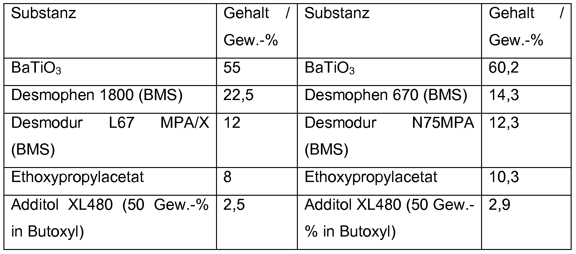
EL-SchichtEL layer
Das erfindungsgemäße EL-Element umfasst mindestens eine EL-Schicht, Komponente BC. Die mindestens eine EL-Schicht kann auf der gesamten Innenfläche der ersten teilweise transparenten Elektrode angeordnet sein oder auf einer oder mehreren Teilflächen der ersten zumindest teilweise transparenten Elektrode. In dem Fall, dass die EL-Schicht auf mehreren Teilflächen angeordnet ist, haben die Teilflächen im Allgemeinen einen Abstand von 0,5 bis 10,0 mm, bevorzugt 1 bis 5 mm voneinander.The EL element according to the invention comprises at least one EL layer, component BC. The at least one EL layer may be arranged on the entire inner surface of the first partially transparent electrode or on one or more partial surfaces of the first at least partially transparent electrode. In the case that the EL layer is arranged on a plurality of partial surfaces, the partial surfaces generally have a spacing of 0.5 to 10.0 mm, preferably 1 to 5 mm from each other.
Die EL-Schicht ist im Allgemeinen aus einer Bindemittelmatrix mit darin homogen dispergierten EL-Pigmenten aufgebaut. Die Bindemittelmatrix wird im Allgemeinen so gewählt, dass ein guter Haftverbund auf der Elektrodenschicht (bzw. der gegebenenfalls darauf aufgebrachten dielektrischen Schicht gegeben ist. In einer bevorzugten Ausführung werden dabei PVB oder PU basierende Systeme verwendet. Neben den EL-Pigmenten können gegebenenfalls noch weitere Zusätze in der Bindemittelmatrix vorliegen, wie farbkonvertierende organische und/oder anorganische Systeme, Farbzusatzstoffe für einen Tag- und Nacht-Lichteffekt und/oder reflektierende und/oder Licht absorbierende Effektpigmente wie Aluminiumflakes oder Glasflakes oder Mica-Plateletts.
-COThe EL layer is generally composed of a binder matrix having homogeneously dispersed EL pigments therein. The binder matrix is generally chosen such that there is a good adhesion on the electrode layer (or the dielectric layer applied thereon, in a preferred embodiment, PVB or PU based systems are used.) In addition to the EL pigments, further additives may optionally be used present in the binder matrix, such as color-converting organic and / or inorganic systems, color additives for a day and night light effect and / or reflective and / or light-absorbing effect pigments such as aluminum flakes or glass flakes or mica platelets. CO
Die in der EL-Schicht verwendeten EL-Pigmente weisen im Allgemeinen eine Dicke von 1 bis 50 μm, vorzugsweise 5 bis 25 μm auf.The EL pigments used in the EL layer generally have a thickness of 1 to 50 μm, preferably 5 to 25 μm.
Bevorzugt ist die mindestens eine EL-Schicht BC eine Wechselstrom-Dickfilm- Pulver-Elektrolumineszenz (AC-P-EL)-Leuchtstruktur.Preferably, the at least one EL layer BC is an AC thick film powder electroluminescent (AC-P-EL) light structure.
Dickfilm AC-EL Systeme sind seit Destriau 1947 gut bekannt und werden meist mittels Siebdruck auf ITO-PET Folien appliziert. Da zinksulfidische Elektroluminophore im Betrieb und speziell bei höheren Temperaturen und einer Wasserdampfumgebung eine sehr starke Degradation aufweisen, werden heute für langlebige Dickfilm AC-EL Lampenaufbauten im Allgemeinen mikroverkapselte EL-Pigmente verwendet. Es ist jedoch ebenfalls möglich, in dem erfindungsgemäßen EL-Element nicht mikroverkapselte Pigmente einzusetzen, wie nachstehend weiter ausgeführt wird.Thick film AC-EL systems have been well-known since Destriau 1947 and are usually applied by screen printing on ITO-PET films. Since zinc sulfide electroluminophores have a very high degradation during operation and especially at higher temperatures and a water vapor environment, microencapsulated EL pigments are generally used today for long-lived thick film AC-EL lamp assemblies. However, it is also possible to use non-microencapsulated pigments in the EL element according to the invention, as further explained below.
Unter EL-Elementen werden im Sinne der vorliegenden Erfindung Dickfilm-EL Systeme verstanden, die mittels Wechselspannung bei normativ 100 Volt und 400 Hertz betrieben werden und derart ein so genanntes kaltes Licht von einigen cd/m2 bis zu einigen 100 cd/m2 emittieren. In derartigen anorganischen Dickfilm-Wechselspannungs-EL-Elementen werden im Allgemeinen EL- Siebdruckpasten verwendet.For the purposes of the present invention, EL elements are thick-film EL systems which are operated by means of alternating voltage at normative 100 V and 400 Hertz and thus emit a so-called cold light of a few cd / m 2 up to a few 100 cd / m 2 , In such inorganic thick film AC EL elements, EL screen pastes are generally used.
Derartige EL-Siebdruckpasten werden im Allgemeinen auf Basis anorganischer Substanzen aufgebaut. Geeignete Substanzen sind beispielsweise hochreine ZnS, CdS, ZnxCdi-xS Verbindungen der Gruppen Il und IV des Periodensystems der Elemente, wobei besonders bevorzugt ZnS eingesetzt wird. Die vorstehend genannten Substanzen können dotiert oder aktiviert werden und gegebenenfalls des Weiteren coaktiviert werden. Zur Dotierung werden beispielsweise Kupfer und/oder Mangan eingesetzt. Die Coaktivierung erfolgt beispielsweise mit Chlor, Brom, lod und Aluminium. Der Gehalt an Alkali- und Selten-Erd-Metallen ist in den vorstehend genannten Substanzen im Allgemeinen sehr gering, falls diese überhaupt vorliegen. Ganz besonders bevorzugt wird ZnS eingesetzt, das bevorzugt mit Kupfer und/oder Mangan
dotiert beziehungsweise aktiviert wird und bevorzugt mit Chlor, Brom, lod und/oder Aluminium coaktiviert wird.Such EL screen-printing pastes are generally based on inorganic substances. Suitable substances are, for example, high-purity ZnS, CdS, Zn x Cdi -x S compounds of groups II and IV of the Periodic Table of the Elements, with ZnS being particularly preferably used. The aforementioned substances may be doped or activated and optionally further co-activated. For doping, for example, copper and / or manganese are used. Coactivation takes place, for example, with chlorine, bromine, iodine and aluminum. The content of alkali and rare earth metals is generally very low in the abovementioned substances, if they are present at all. Most preferably ZnS is used, preferably with copper and / or manganese is doped or activated and is preferably co-activated with chlorine, bromine, iodine and / or aluminum.
Übliche EL-Emissionsfarben sind gelb, grün, grün-blau, blau-grün und weiß, wobei die Emissionsfarbe weiß oder rot durch Mischungen geeigneter EL-Common EL emission colors are yellow, green, green-blue, blue-green and white, the emission color being white or red by mixtures of suitable EL dyes.
Pigmente gewonnen werden kann oder durch Farbkonversion. DiePigments can be obtained or by color conversion. The
Farbkonversion kann im Allgemeinen in Form einer konvertierenden Schicht und/oder der Beimengung entsprechender Farbstoffe und Pigmente in den polymeren Binder der Siebdruckfarben beziehungsweise der polymeren Matrix, in die die EL-Pigmente eingebaut sind, erfolgen.Color conversion can generally take place in the form of a converting layer and / or the addition of corresponding dyes and pigments in the polymeric binder of the screen printing inks or the polymeric matrix in which the EL pigments are incorporated.
In einer weiteren Ausführungsform der vorliegenden Erfindung sind die zur Herstellung der EL-Schicht eingesetzte Siebdruckmatrix mit lasierenden, farbfilternden oder mit farbkonvertierenden Farbstoffen und/oder Pigmenten versehen sind. Auf diese Weise kann eine Emissionfarbe Weiß oder ein Tag- Nacht-Lichteffekt generiert werden.In a further embodiment of the present invention, the screen printing matrix used to produce the EL layer is provided with translucent, color-filtering or color-converting dyes and / or pigments. In this way, an emission color white or a day-night light effect can be generated.
In einer weiteren Ausführungsform werden in der EL-Schicht Pigmente eingesetzt, die eine Emission im blauen Wellenlängenbereich von 420 bis 480 nm aufweisen und mit einer farbkonvertierenden Mikroverkapselung versehen sind. Auf diese Weise kann die Farbe Weiß emittiert werden.In a further embodiment, pigments are used in the EL layer which have an emission in the blue wavelength range from 420 to 480 nm and are provided with a color-converting microencapsulation. In this way, the color white can be emitted.
In einer Ausführungsform werden als Pigmente in der EL-Schicht AC-P-EL- Pigmente eingesetzt, die eine Emission im blauen Wellenlängenbereich von 420 bis 480 nm aufweisen. Zusätzlich weist die AC-P-EL Siebdruckmatrix bevorzugt wellenlängenkonventierende anorganische feine Partikel auf Basis von Europium (II) aktivierten Erdalkali-ortho-Silikat Phosphoren wie (Ba, Sr, Ca)2SiO4:Eu2+ oder YAG Phosphoren wie Y3AI5Oi2)Ce3+ oder Tb3AI5Oi2)Ce3+ oder Sr2GaS4)Eu2+ oder SrS:Eu2+ oder (Y1Lu, Gd1Tb)3(AI1Sc1Ga)5Oi2)Ce3+ oder (Zn,Ca,Sr)(S,Se):Eu2+ auf. Auch auf diese Weise kann eine weiße Emission erzielt werden.In one embodiment, as pigments in the EL layer AC-P-EL pigments are used which have an emission in the blue wavelength range of 420 to 480 nm. In addition, the AC-P-EL screen printing matrix preferably comprises wavelength-controlling inorganic fine particles based on europium (II) activated alkaline earth ortho-silicate phosphors such as (Ba, Sr, Ca) 2 SiO 4 : Eu 2+ or YAG phosphors such as Y 3 Al 5 Oi 2 ) Ce 3+ or Tb 3 Al 5 Oi 2 ) Ce 3+ or Sr 2 GaS 4 ) Eu 2+ or SrS: Eu 2+ or (Y 1 Lu, Gd 1 Tb) 3 (Al 1 Sc 1 Ga ) 5 Oi 2 ) Ce 3+ or (Zn, Ca, Sr) (S, Se): Eu 2+ . Also in this way a white emission can be achieved.
Entsprechend dem Stand der Technik können die vorstehen genannten EL- Pigmente mikroverkapselt werden. Durch die anorganische
Mikroverkapselungstechnologie sind gute Halbwertszeiten erzielbar. Beispielhaft sei hier das EL-Siebdrucksystem Luxprint® for EL der Firma E. I. du Pont de Nemours and Companies genannt. Organischen Mikroverkapselungstechnologien und Folienhüll-Laminate auf Basis der diversen thermoplastischen Folien sind grundsätzlich ebenfalls geeignet, haben sich jedoch als teuer und nicht wesentlich lebensdauerverlängernd erwiesen.According to the prior art, the above-mentioned EL pigments can be microencapsulated. By the inorganic Microencapsulation technology achieves good half-lives. As an example, the EL screen printing system Luxprint ® for EL of the company EI du Pont de Nemours and Companies mentioned. Organic microencapsulation technologies and film-wrap laminates based on the various thermoplastic films are also generally suitable, but have proven to be expensive and not significantly extended in life.
Geeignete zinksulfidische mikroverkapselte EL-Pigmente werden von der Firma Osram Sylvania, Inc. Towanda unter dem Handelsnamen GlacierGLO™ Standard, High Brite und Long Life und von der Firma Durel Division der Rogers Corporation, unter den Handelsnamen 1 PHS001® High-Efficiency Green Encapsulated EL Phosphor, 1 PHS002® High-Efficiency Blue-Green Encapsulated EL Phosphor, 1 PHS003® Long-Life Blue Encapsulated EL Phosphor, 1 PHS004® Long-Life Orange Encapsulated EL Phosphor, angeboten.Suitable zinc sulfide microencapsulated EL pigments are sold by Osram Sylvania, Inc. Towanda under the trade name GlacierGLO ™ Standard, High Brite and Long Life and the Durel Division of Rogers Corporation, under the trade names 1 PHS001 ® High-Efficiency Green Encapsulated EL phosphorus, 1 PHS002 ® high-Efficiency Blue-Green Encapsulated EL phosphor, 1 PHS003 ® Long-Life Blue Encapsulated EL phosphor, 1 PHS004 ® Long-Life Orange Encapsulated EL phosphor offered.
Die mittleren Teilchendurchmesser der in der EL-Schicht geeigneten mikroverkapselten Pigmente betragen im Allgemeinen 15 bis 60 μm, bevorzugt 20 bis 35 μm.The average particle diameters of the microencapsulated pigments suitable in the EL layer are generally 15 to 60 μm, preferably 20 to 35 μm.
In der EL-Schicht des erfindungsgemäßen EL-Elements können auch nicht mikroverkapselte feinkörnige EL-Pigmente, bevorzugt mit einer hohen Lebensdauer, eingesetzt werden. Geeignete nicht mikroverkapselte feinkörnige zinksulfidische EL-Pigmente sind beispielsweise in US 6,248,261 und in WO 01/34723 offenbart. Diese weisen bevorzugt ein kubisches Kristal Igefüge auf. Die nicht mikroverkapselten Pigmente haben bevorzugt mittlere Teilchendurchmesser von 1 bis 30 μm, besonders bevorzugt 3 bis 25 μm, ganz besonders bevorzugt 5 bis 20 μm.Non-microencapsulated fine-grained EL pigments, preferably having a long service life, can also be used in the EL layer of the EL element according to the invention. Suitable non-microencapsulated fine-grained zinc sulfide EL pigments are disclosed, for example, in US 6,248,261 and in WO 01/34723. These preferably have a cubic crystal structure. The non-microencapsulated pigments preferably have average particle diameters of from 1 to 30 .mu.m, particularly preferably from 3 to 25 .mu.m, very particularly preferably from 5 to 20 .mu.m.
Speziell nicht mikroverkapselte EL-Pigmente können mit kleineren Pigmentabmessungen bis unter 10 μm verwendet werden. Dadurch kann die Durchsichtigkeit des Glaselementes erhöht werden.
Somit können den gemäß der vorliegenden Anmeldung geeigneten Siebdruckfarben unverkapselte Pigmente beigemengt werden, bevorzugt unter Berücksichtigung der speziellen hygroskopischen Eigenschaften der Pigmente, bevorzugt der ZnS-Pigmente. Dabei werden im Allgemeinen Bindemittel verwendet, die einerseits eine gute Adhäsion zu sogenannten ITO-Schichten (Indium-ZinnOxid) oder intrinsisch leitfähige polymeren transparenten Schichten haben, und des Weiteren gut isolierend wirken, das Dielektrikum verstärken und damit eine Verbesserung der Durchschlagsfestigkeit bei hohen elektrischen Feldstärken bewirken und zusätzlich im ausgehärteten Zustand eine gute Wasserdampfsperre aufweisen und die EL-Pigmente zusätzlich schützen und lebensdauerverlängernd wirken.Specially non-microencapsulated EL pigments can be used with smaller pigment dimensions down to less than 10 μm. As a result, the transparency of the glass element can be increased. Thus, non-encapsulated pigments can be added to the screen printing inks suitable according to the present application, preferably taking into account the special hygroscopic properties of the pigments, preferably the ZnS pigments. In this case, binders are generally used which, on the one hand, have good adhesion to so-called ITO layers (indium-tin oxide) or intrinsically conductive polymeric transparent layers, and furthermore have good insulating properties, reinforce the dielectric and thus improve the dielectric strength at high electric field strengths cause and additionally in the cured state have a good water vapor barrier and additionally protect the EL pigments and extend life span.
In einer Ausführungsform der vorliegenden Erfindung werden in der AC-P-EL- Leuchtschicht Pigmente eingesetzt, die nicht mikroverkapselt sind.In one embodiment of the present invention, pigments which are not microencapsulated are used in the AC-P-EL luminescent layer.
Die Halbwertzeiten der geeignete Pigmente in der EL-Schicht, also jene Zeit, in der die Initialhelligkeit des erfindungsgemäßen EL-Elements auf die Hälfte abgesunken ist, betragen im Allgemeinen bei 100 bzw. 80 Volt und 400 Hertz 400 bis maximal 5000 Stunden, üblicherweise jedoch nicht mehr als 1000 bis 3500 Stunden.The half-lives of the suitable pigments in the EL layer, ie the time in which the initial brightness of the EL element according to the invention has fallen to half, are generally at 100 or 80 volts and 400 hertz 400 to a maximum of 5000 hours, but usually not more than 1000 to 3500 hours.
Die Helligkeitswerte (EL-Emission) betragen im Allgemeinen 1 bis 200 cd/m2, bevorzugt 3 bis 100 cd/m2, besonders bevorzugt bei 5 bis 40 cd/m2; bei großen Leuchtflächen liegen die Helligkeitswerte bevorzugt im Bereich von 1 bis 50 cd/m2.The brightness values (EL emission) are generally 1 to 200 cd / m 2 , preferably 3 to 100 cd / m 2 , particularly preferably 5 to 40 cd / m 2 ; For large illuminated areas, the brightness values are preferably in the range from 1 to 50 cd / m 2 .
Es können jedoch auch Pigmente mit längeren oder kürzeren Halbwertszeiten und höheren oder niedrigeren Helligkeitswerten in der EL-Schicht des erfindungsgemäßen EL-Elements eingesetzt werden.However, it is also possible to use pigments with longer or shorter half-lives and higher or lower brightness values in the EL layer of the EL element according to the invention.
In einer weiteren Ausführungsform der vorliegenden Erfindung weisen die in der EL-Schicht vorliegenden Pigmente einen derart kleinen mittleren Teilchendurchmesser auf, beziehungsweise einen derart geringen Füllgrad in der EL-Schicht, beziehungsweise die einzelnen EL-Schichten sind geometrisch
ά-In a further embodiment of the present invention, the pigments present in the EL layer have such a small average particle diameter, or such a low degree of filling in the EL layer, or the individual EL layers are geometrical ά-
derart klein ausgeführt, beziehungsweise der Abstand der einzelnen EL- Schichten wird derart groß gewählt, so dass das EL-Element bei nicht elektrisch aktivierter Leuchtstruktur als zumindest teilweise durchsichtig gestaltet ist beziehungsweise eine Durchsicht gewährleistet ist. Geeignete Pigmentteilchendurchmesser, Füllgrade, Abmessungen der Leuchtelemente und Abstände der Leuchtelemente sind vorstehend genannt.executed so small, or the distance between the individual EL layers is chosen so large, so that the EL element is designed as not transparent at least partially transparent in the case of a non-electrically activated lighting structure or a view is ensured. Suitable pigment particle diameters, fill levels, dimensions of the luminous elements and distances of the luminous elements are mentioned above.
Die Schicht enthält die oben genannten gegebenenfalls dotierten ZnS-Kristalle, bevorzugt wie oben beschrieben mikroverkapselt, vorzugsweise in einer Menge von 40 bis 90 Gew.-%, bevorzugt von 50 bis 80 Gew.-%, besonders bevorzugt 55 bis 70 Gew.-%, jeweils bezogen auf das Gewicht der Paste. Als Bindemittel können Ein- und bevorzugt Zweikomponentenpolyurethane verwendet werden. Erfindungsgemäß bevorzugt sind hochflexible Materialien der Bayer MaterialScience AG, beispielsweise die Lackrohstoffe der Desmophen- und Desmodur-Reihen, vorzugsweise Desmophen und Desmodur, oder die Lackrohstoffe der Lupranate-, Lupranol-, Pluracol- oder Lupraphen-Reihen der BASF AG. Als Lösemittel können Ethoxypropylacetat, Ethylacetat, Butylacetat, Methoxypropylacetat, Aceton, Methylethylketon, Methyl isobutylketon, Cyclohexanon, Toluol, XyIoI, Solventnaphtha 100 oder beliebige Mischungen von zwei oder mehreren dieser Lösemittel in Mengen von vorzugsweise 1 bis 50 Gew.-%, bevorzugt 2 bis 30 Gew.-%, besonders bevorzugt 5 bis 15 Gew.-%, jeweils bezogen auf die Gesamtpastenmasse, verwendet werden. Weiterhin können andere hochflexible Bindemittel, zum Beispiel solche auf Basis von PMMA, PVA, insbesondere Mowiol und Poval von Kuraray Europe GmbH (heißt jetzt Kuraray Specialties oder Polyviol von Wacker AG, oder PVB, inbesondere Mowital von Kuraray Europe GmbH (B 20 H, B 30 T, B 30 H, B 30 HH, B 45 H, B 60 T, B 60 H, B 60 HH, B 75 H), oder Pioloform, insondere Pioloform BR18, BM18 oder BT18, von Wacker AG, sein. Bei Verwendung von Polymerbindemittel wie zum Beispiel PVB können weiterhin Lösungsmittel wie Methanol, Ethanol, Propanol, Isopropanol, Diacetonalkohol, Benzylalkohol, 1 - Methoxypropanol-2, Butylglykol, Methoxybutanol, Dowanol,The layer contains the abovementioned optionally doped ZnS crystals, preferably microencapsulated as described above, preferably in an amount of from 40 to 90% by weight, preferably from 50 to 80% by weight, particularly preferably from 55 to 70% by weight. , in each case based on the weight of the paste. As binders, one- and preferably two-component polyurethanes can be used. According to the invention, highly flexible materials from Bayer MaterialScience AG are preferred, for example the lacquer raw materials of the desmophen and desmodur series, preferably desmophen and desmodur, or the lacquer raw materials of the Lupranate, Lupranol, Pluracol or Lupraphen series from BASF AG. As solvents ethoxypropyl acetate, ethyl acetate, butyl acetate, methoxypropyl acetate, acetone, methyl ethyl ketone, methyl isobutyl ketone, cyclohexanone, toluene, xylene, solvent naphtha 100 or any mixtures of two or more of these solvents in amounts of preferably 1 to 50 wt .-%, preferably 2 to 30 wt .-%, particularly preferably 5 to 15 wt .-%, each based on the total paste mass, are used. Furthermore, other highly flexible binders, for example those based on PMMA, PVA, in particular Mowiol and Poval from Kuraray Europe GmbH (now called Kuraray Specialties or Polyviol from Wacker AG, or PVB, in particular Mowital from Kuraray Europe GmbH (B 20 H, B 30 T, B 30 H, B 30 HH, B 45 H, B 60 T, B 60 H, B 60 HH, B 75 H), or Pioloform, in particular Pioloform BR18, BM18 or BT18, from Wacker AG Use of polymer binders such as PVB may further solvents such as methanol, ethanol, propanol, isopropanol, diacetone alcohol, benzyl alcohol, 1 - methoxypropanol-2, butyl glycol, methoxybutanol, Dowanol,
Methoxypropylacetat, Methylacetat, Ethylacetat, Butylacetat, Butoxyl, Glykolsäure-n-butylester. Aceton, Methylethylketon, Methyl isobutylketon, Cyclohexanon, Toluol, XyIoI, Hexan, Cyclohexan, Heptan sowie Mischungen
aus zwei oder mehreren der genannten in Mengen von 1 bis 30 Gew.-% bezogen auf die Gesamtmasse der Paste, bevorzugt 2 bis 20 Gew.%, besonders bevorzugt 3 bis 10 Gew.-% zugesetzt werden.Methoxypropyl acetate, methyl acetate, ethyl acetate, butyl acetate, butoxyl, glycolic acid n-butyl ester. Acetone, methyl ethyl ketone, methyl isobutyl ketone, cyclohexanone, toluene, xylene, hexane, cyclohexane, heptane and mixtures from two or more of the mentioned in amounts of 1 to 30 wt .-% based on the total mass of the paste, preferably 2 to 20 wt.%, Particularly preferably 3 to 10 wt .-% are added.
Weiterhin können 0,1 bis 2 Gew.-% Additive zur Verbesserung des Fließverhaltens und des Verlaufs enthalten sein. Beispiele für Verlaufsmittel sind Additol XL480 in Butoxyl in einem Mischungsverhältnis von 40:60 bis 60:40. Als weitere Additive können 0,01 bis 10 Gew.-%, bevorzugt 0,05 bis 5 Gew.-%, besonders bevorzugt 0,1 bis 2 Gew.-%, jeweils bezogen aus die Gesamtpastenmasse, Rheologieadditive enthalten sein, die das Absetzverhalten von Pigmenten und Füllstoffen in der Paste vermindern, beispielsweise BYK 410, BYK 411 , BYK 430, BYK 431 oder beliebige Mischungen davon.Furthermore, 0.1 to 2 wt .-% additives to improve the flow behavior and the course may be included. Examples of flow control agents are Additol XL480 in butoxyl in a mixing ratio of 40:60 to 60:40. 0.01 to 10 wt .-%, preferably 0.05 to 5 wt .-%, particularly preferably 0.1 to 2 wt .-%, each based on the total paste mass, rheology additives which contain the settling behavior can be included as further additives of pigments and fillers in the paste, for example BYK 410, BYK 411, BYK 430, BYK 431 or any mixtures thereof.
Erfindungsgemäß besonders bevorzugte Formulierungen von Druckpasten zur Herstellung der EL-Pigmentschicht als Komponente BC enthalten:Particularly preferred formulations of printing pastes according to the invention for producing the EL pigment layer as component BC include:


Darüber hinaus können auch kommerziell erhältliche, bereits fertig abgemischte Siebdruckpasten verwendet werden, beispielsweise solche der Hersteller Metalor oder Norcote.In addition, it is also possible to use commercially available, already ready-mixed screen printing pastes, for example those from Metalor or Norcote.
Abdeckschichtcovering
Neben den Komponenten A und B enthält das erfindungsgemäße EL-Element eine Schutzschicht, Komponente CA, um eine Zerstörung desIn addition to the components A and B, the EL element according to the invention contains a protective layer, component CA, in order to destroy the
Elektrolumineszenz-Elements bzw. der gegebenenfalls vorhandenen graphischen Darstellungen zu vermeiden. Geeignete Materialien derElectroluminescent element or the optionally present graphical representations to avoid. Suitable materials of
Schutzschicht sind dem Fachmann bekannt. Geeignete Schutzschichten CA sind beispielsweise hochtemperaturbeständige Schutzlacke wie Schutzlacke, die Polycarbonate und Bindemittel enthalten. Ein Beispiel für einen solchenProtective layer are known in the art. Suitable protective layers CA are, for example, high-temperature-resistant protective lacquers, such as conformal lacquers containing polycarbonates and binders. An example of such
Schutzlack ist Noriphan® HTR von Pröll, Weißenburg.Protective lacquer is Noriphan HTR ® by Proell, Weissenburg.
Alternativ kann die Schutzschicht auch auf Basis von flexiblen Polymeren wie Polyurethanen, PMMA, PVA, PVB formuliert werden. Hierfür können Polyurethane von Bayer MatehalScience AG verwendet werden. Diese Formulierung kann auch mit Füllstoffen versehen sein. Hierfür geeignet sind alle dem Fachmann bekannten Füllstoffe, beispielsweise auf Basis anorganischer Metalloxide wie ÜO2, ZnO, Lithopone, etc mit einem Füllgrad von 10 bis 80 Gew.% der Druckpaste, bevorzugt von 20 bis 70 %, besonders bevorzugt von 40 bis 60 %. Weiterhin können die Formulierungen Verlaufsmittel sowie Rheologieadditive enthalten. Als Lösemittel können beispielsweise.
Ethoxypropylacetat, Ethylacetat, Butylacetat, Methoxypropylacetat, Aceton, Methylethylketon, Methyl isobutylketon, Cyclohexanon, Toluol, XyIoI, Solventnaphtha 100 oder Mischungen aus zwei oder mehreren dieser Lösemittel verwendet werden.Alternatively, the protective layer can also be formulated on the basis of flexible polymers such as polyurethanes, PMMA, PVA, PVB. Polyurethanes from Bayer MatehalScience AG can be used for this purpose. This formulation can also be provided with fillers. Suitable for this purpose are all fillers known to the person skilled in the art, for example based on inorganic metal oxides such as O 2 O, ZnO, lithopone, etc. with a degree of filling of 10 to 80% by weight of the printing paste, preferably from 20 to 70%, particularly preferably from 40 to 60%. Furthermore, the formulations may contain leveling agents as well as rheology additives. As a solvent, for example. Ethoxypropylacetat, ethyl acetate, butyl acetate, methoxypropyl acetate, acetone, methyl ethyl ketone, methyl isobutyl ketone, cyclohexanone, toluene, xylene, solvent naphtha 100 or mixtures of two or more of these solvents may be used.
Erfindungsgemäß besonders bevorzugte Formulierungen des Schutzlackes CA enthalten zum Bespiel:According to the invention, particularly preferred formulations of the protective lacquer CA include, for example:


Substratesubstrates
Das erfindungsgemäße EL-Element kann auf einer oder auf beiden Seiten an den jeweiligen Elektroden Substrate, wie beispielsweise Gläser, Kunststofffolien oder dergleichen aufweisen.The EL element according to the invention may have on one or both sides of the respective electrodes substrates, such as glasses, plastic films or the like.
Bei dem erfindungsgemäßen EL-Element ist es bevorzugt, dass zumindest das Substrat, welches mit der transparenten Elektrode in Kontakt steht, innenseitig
grafisch lasierend transluzent und opak abdeckend gestaltet ist. Unter einer opaken abdeckenden Gestaltung wird ein großflächiger Elektrolumineszenzbereich verstanden, der durch eine hochauflösende grafische Gestaltung opak abgedeckt wird und/oder lasierend beispielsweise im Sinne von rot - grün - blau transluzent für Signalzwecke ausgebildet ist.In the EL element of the present invention, it is preferable that at least the substrate in contact with the transparent electrode is inside Graphically translucent and opaque covering designed. An opaque covering design is understood to be a large-area electroluminescent region which is opacified by a high-resolution graphic design and / or is designed to be translucent, for example in the sense of red-green-blue translucent, for signal purposes.
Darüber hinaus ist es bevorzugt, dass das Substrat, welches mit der transparenten Elektrode BA in Kontakt steht, eine Folie ist, welche unterhalb Glasübergangstemperatur Tg kaltreckbar verformbar ist. Hierdurch ergibt sich die Möglichkeit, dass resultierende EL-Element dreidimensional zu verformen.Moreover, it is preferred that the substrate, which is in contact with the transparent electrode BA, is a film which is cold-stretchable under glass transition temperature Tg. This gives rise to the possibility of deforming the resulting EL element three-dimensionally.
Darüber hinaus ist es bevorzugt, dass das Substrat, welches mit der Rückelektrode BE in Kontakt steht eine, Folie ist, welche ebenfalls unterhalb Tg kaltreckbar verformbar ist. Hierdurch ergibt sich die Möglichkeit, dass resultierende EL-Element dreidimensional zu verformen.Moreover, it is preferred that the substrate, which is in contact with the back electrode BE, is a film which is also cold stretchable below Tg. This gives rise to the possibility of deforming the resulting EL element three-dimensionally.
Darüber hinaus ist es bevorzugt, dass das EL-Element dreidimensional verformbar ist und insbesondere unterhalb Tg kaltreckbar verformbar ist und derart eine präzise geformte dreidimensionale Gestalt erhält.Moreover, it is preferred that the EL element is three-dimensionally deformable and in particular is cold bendable deformable below Tg and thus obtains a precisely shaped three-dimensional shape.
Das dreidimensional verformte Element kann in einem Spritzgusswerkzeug auf zumindest einer Seite mit einem thermoplastischen Kunststoff angeformt werden.The three-dimensionally deformed element can be formed in an injection molding tool on at least one side with a thermoplastic material.
Herstellung erfindungsgemäßer EL-ElementeProduction of inventive EL elements
Üblicherweise werden die vorstehend genannten Pasten (Siebdruckpasten) auf transparente Kunststoff-Folien oder Gläser aufgebracht, die wiederum eine weitgehend transparente elektrisch leitende Beschichtung aufweisen und dadurch die Elektrode für die Sichtseite darstellen. Anschließend werden drucktechnisch und/oder laminationstechnisch das Dielektrikum, soweit vorhanden, und die Rückseitenelektrode hergestellt.
Es ist jedoch ebenfalls ein umgekehrter Herstellungsprozess möglich, wobei zunächst die Rückseitenelektrode hergestellt wird oder die Rückseitenelektrode in Form einer metallisierten Folie verwendet wird und auf diese Elektrode das Dielektrikum aufgetragen wird. Anschließend werden die EL-Schicht und daran anschließend die transparente und elektrisch leitende obere Elektrode aufgetragen. Das erhaltene System kann anschließend gegebenenfalls mit einer transparenten Deckfolie laminiert und damit gegen Wasserdampf bzw. auch gegen mechanische Beschädigung geschützt werden.Usually, the above pastes (screen printing pastes) are applied to transparent plastic films or glasses, which in turn have a substantially transparent electrically conductive coating and thereby represent the electrode for the visible side. Subsequently, the dielectric, if present, and the backside electrode are produced by printing technology and / or lamination technology. However, a reverse manufacturing process is also possible, wherein first the backside electrode is made or the backside electrode is used in the form of a metallized film and the dielectric is applied to this electrode. Subsequently, the EL layer and then the transparent and electrically conductive upper electrode are applied. The system obtained can then optionally be laminated with a transparent cover sheet and thus protected against water vapor or against mechanical damage.
In einer Ausführungsform der Erfindung können die Leiterbahnen (Silberbus) als erste Schicht auf das Substrat A aufgebracht werden. Erfindungsgemäß bevorzugt werden sie jedoch auf die Elektroden BA bzw. BE, entweder in zwei Arbeitsgängen jeweils einzeln auf die Elektroden, oder in einem Arbeitschritt die Elektroden gemeinsam.In one embodiment of the invention, the conductor tracks (silver bus) can be applied as a first layer to the substrate A. According to the invention, however, they are preferably applied to the electrodes BA or BE, either individually in two operations on the electrodes, or in one working step, the electrodes together.
Die EL-Schicht wird üblicherweise drucktechnisch mittels Siebdruck oder Dispenserauftrag oder InkJet-Auftrag oder auch mit einem Rakelvorgang oder einem Rollenbeschichtungsverfahren oder einem Vorhanggießverfahren oder einem Transferverfahren, bevorzugt mittels Siebdruck, aufgebracht. Bevorzugt wird die EL-Schicht auf die Oberfläche der Elektrode oder auf die gegebenenfalls auf die Rückelektrode aufgebrachte Isolationsschicht aufgebracht.The EL layer is usually applied by printing by means of screen printing or dispenser application or inkjet application or else by a doctor blade process or a roller coating process or a curtain casting process or a transfer process, preferably by screen printing. Preferably, the EL layer is applied to the surface of the electrode or to the optionally applied to the back electrode insulation layer.
Als Energieversorgung (5) wird bevorzugt eine aufladbare Batterie verwendet und können relativ kleine beziehungsweise flache Batterien mit guter Aufladcharakteristik und geringer Entladecharakteristik verwendet werden.As the power supply (5), a rechargeable battery is preferably used, and relatively small or flat batteries having a good charging characteristic and a low discharging characteristic can be used.
Beispielsweise bietet die Firma Solicore, Inc. eine bis 135°C laminierfähige aufladbare Flachbatterie SF-7624-HT40EA038 mit den Abmessungen 76 x 24 mm und einer Dicke im Bereich 0,38 bis 0,45 mm mit einer nominalen Kapazität von 40 mAh und nominal 3 Volt bei einem Strompulsleistungsvermögen von bis zu 40 mA an.
Moderne EL-Inverter (3) können bereist ab 3 VoIt-DC betrieben werden und benötigen geringe Ströme. Beispielsweise bietet die Firma Supertex Inc. einen EL-Lamp-Driver-IC HV850 mit den Abmessungen 4,9 x 2,95 x 1 ,1 mm und der Betriebsspannung 3,0 bis 4,2 VoIt-DC an. Damit kann eine EL-Anordnung mit einer Abmessung, wie sie bei Mobiltelefondisplays üblich ist, mit Wechselspannungen im Bereich 100 Volt bis über 200 Volt bei Frequenzen ab 50 Hz, typisch bei etwa 200 Hz bis 800Hz bis in den kHz-Bereich, betrieben werden.For example, Solicore, Inc. offers a 135 ° C laminatable SF-7624-HT40EA038 rechargeable flat battery with dimensions of 76 x 24 mm and a thickness in the range of 0.38 to 0.45 mm with a nominal capacity of 40 mAh and nominal 3 volts with a current pulse performance of up to 40 mA. Modern EL inverters (3) can be operated from 3 VoIt DC and require low currents. For example, Supertex Inc. offers an HV850 EL Lamp Driver IC measuring 4.9 x 2.95 x 1, 1 mm and operating voltage 3.0 to 4.2 Volts DC. Thus, an EL device with a dimension, as is common in mobile phone displays, with AC voltages in the range of 100 volts to over 200 volts at frequencies from 50 Hz, typically at about 200 Hz to 800Hz up to the kHz range, operated.
Als mögliche EL-Fläche werden 2 in2 angegeben. Im vorliegenden Fall werden nur einige wenige 2 bis maximal 10 cd/m2 EL-Emissionshelligkeit benötigt. Dieser HV850 IC bietet überdies noch zusätzliche elektronische Besonderheiten, wie die Regelbarkeit der EL-Frequenz oder dem verzögerten Ausschalten und dergleichen Zusatzfunktionen. Dieser HV850 benötigt überdies keine zusätzliche Induktivität (Spule) zum Betrieb einer EL-FoNe und ist deshalb für eine extrem flache Bauweise besonders gut geeignet.As a possible EL area 2 in 2 are given. In the present case only a few 2 to a maximum of 10 cd / m 2 EL emission brightness are needed. This HV850 IC also offers additional electronic features, such as the controllability of the EL frequency or the delayed switch off and the like additional functions. Moreover, this HV850 requires no additional inductance (coil) for operating an EL-FoNe and is therefore particularly well suited for an extremely flat design.
Es gibt allerdings eine Reihe von alternativen EL-Lampen-Treiberschaltungen, die ebenfalls bereits mit 3 VoIt-DC betrieben werden können und ebenfalls eine sehr dünne Bauweise aufweisen und oft Zusatzeinrichtungen für den Betrieb von zwei EL-Feldern beinhalten oder eine Power-down Elektronik oder eine Sensor gesteuerte Helligkeitsregelung.There are, however, a number of alternative EL lamp driver circuits which can also be powered by 3 VoIt-DCs and are also very thin in construction and often include ancillary equipment for the operation of two EL panels or a power-down electronics or power supply a sensor-controlled brightness control.
Der Ein-Aus-Schalter (6) beziehungsweise Taster kann in vielfältiger Art und Weise realisiert werden und kann beispielsweise als kapazitives Feld oder als biegeelastisches Feld ausgebildet werden.The on-off switch (6) or button can be realized in many ways and can be formed for example as a capacitive field or as a flexurally elastic field.
Das Ladeelement (9) kann ebenfalls vielfältig ausgeführt werden. In einer einfachen und kostengünstigen Ausführungsform wird eine Standard Niederspannungs-Ladebuchse bis zu einer Micro-USB Buchse vorgesehen und kann derart mittels ohmschen Kontakts der Batterieladevorgang erfolgen. Neben dieser kontaktbehafteten Ladeform der Batterie können auch kapazitive oder induktive Ladesysteme nach dem Stand der Technik verwendet werden.
In Figur 3 wird ein schematischer Schnitt durch eine zweite Ausführungsform eines EL-Leuchtlaminats (1 ) mit einer Schutzhülle (12) dargestellt. In dieser schematischen Schnittdarstellung bilden zwei Folien (13, 14) die Schutzhülle (12). Grundsätzlich kann anstelle der unteren Folie (14) auch das Substrat (10) als untere Folie verwendet werden.The loading element (9) can also be made diverse. In a simple and inexpensive embodiment, a standard low-voltage charging socket is provided up to a micro-USB socket and can be done by ohmic contact of the battery charging process. In addition to this contact-type charging of the battery and capacitive or inductive charging systems can be used in the prior art. FIG. 3 shows a schematic section through a second embodiment of an EL luminous laminate (1) with a protective cover (12). In this schematic sectional view, two foils (13, 14) form the protective cover (12). In principle, instead of the lower film (14), the substrate (10) can also be used as the lower film.
Die Funktionsbeschriftung (7) erfolgt in diesen Fällen auf der oberen Schutzfolie (13) und das zumindest stückweise Klettverschlußelement (11 ) wird auf der Unterseite der unteren Schutzhülle (14) angeordnet oder auf der Unterseite des Substrats (10). Die Schutzhüllen-Folien (13, 14) können in der Form von thermoplastischen Kunststoff-Folien verwendet werden, wobei zumindest die obere Folie (13) im Bereich der EL-Anordnung transparent oder zumindest transluzent ausgeführt sein muss. Die Schutzhüllen-Folien (13, 14) können auch aus einem Gewebematerial oder einem Wirrflies (Non-woven) Material gebildet werden, wobei zumindest das obere Element (13) im Bereich der EL- Anordnung (2) transparent oder transluzent ausgebildet sein muss.The functional inscription (7) is in these cases on the upper protective film (13) and the at least piece Velcro fastener element (11) is arranged on the underside of the lower protective cover (14) or on the underside of the substrate (10). The protective film (13, 14) can be used in the form of thermoplastic films, wherein at least the upper film (13) in the region of the EL array must be made transparent or at least translucent. The protective film (13, 14) can also be formed from a fabric material or a nonwoven fabric, wherein at least the upper element (13) in the region of the EL array (2) must be transparent or translucent.
In Figur 4 wird ein schematischer Schnitt durch eine erste Ausführungsform eines EL-Leuchtlaminats (1 ) mit einer Schutzhülle (12) und rückseitiger Elektronik (3, 9) dargestellt. Diese Ausführungsform erfordert zwar eine beidseitige Anbringung von Komponenten auf dem Substrat (10) und derart auch eine zweite rückseitige Verdrahtungsstruktur (16), bietet jedoch eine effizientere Flächenausnützung der Vorderseite durch die EL-Anordnung (2) und eine effiziente Ausnützung der Rückseite für die Anordnung einer flachen und dünnen aufladbaren Batterie (5).FIG. 4 shows a schematic section through a first embodiment of an EL luminous laminate (1) with a protective cover (12) and rear-side electronics (3, 9). Although this embodiment requires mounting both components on the substrate (10) on both sides and also a second back wiring structure (16), it provides more efficient front surface utilization by the EL device (2) and efficient utilization of the back side for the device a flat and thin rechargeable battery (5).
In Figur 5 wird eine schematische Darstellung einer Person (17) mit Schutzkleidungselementen (8) und EL-Leuchtlaminaten (1 ) dargestellt. Die EL- Leuchtlaminate (1 ) können derart mittels Klettverschlußbefestigung abnehmbar an einer Vielzahl von Positionen angeordnet werden. Die Anbringung derartiger EL-Leuchtlaminate (1 ) mittels zumindest stückweisen Klettverschlußelementen (11 ) auf Flaschen beziehungsweise Versorgungs- und Einsatzgegenständen kann in analoger Form zur Anbringung auf einer Person (17) erfolgen.
Im Rahmen der vorliegenden Erfindung wird unter einem Laminat insbesondere ein Verbund aus Substrat, Elektrolumineszenz-Element und Schutzhülle verstanden.FIG. 5 shows a schematic representation of a person (17) with protective clothing elements (8) and EL luminescent laminates (1). The EL luminous laminates (1) can be arranged in such a way by means of Velcro fastener detachably at a plurality of positions. The attachment of such EL luminous laminates (1) by means of at least piece Velcro fasteners (11) on bottles or supply and Einsatzgegenständen can take place in analogous form for attachment to a person (17). In the context of the present invention, a laminate is understood in particular to mean a composite of substrate, electroluminescent element and protective cover.
Unter dem begriff „flächig" wird im Rahmen der vorliegenden Erfindung insbesondere verstanden, dass die Anordnung so ausgebildet ist, dass eine Flachbatterien, beispielsweise die bereits erwähnte Flachbatterie SF-7624- HT40EA038 mit den Abmessungen 76 x 24 mm und einer Dicke im Bereich 0,38 bis 0,45 mm, aufgenommen werden kann.In the context of the present invention, the term "planar" is understood in particular to mean that the arrangement is designed such that a flat battery, for example the already mentioned flat battery SF-7624-HT40EA038 with the dimensions 76 × 24 mm and a thickness in the range 0, 38 to 0.45 mm, can be recorded.
Da ein derartiges EL-Leuchtelement in der erfindungsgemäßen Verwendung flexibel verformbar sein muss und unter rauen Einsatzbedingungen verwendet werden soll, wird der EL-Element-Aufbau für große Verformbarkeit ausgelegt. Insbesondere werden dabei Polyurethan basierende Siebdruckfarbensysteme verwendet und wird zumindest für die vordere transparente Elektrode eine biegbare und/oder verformbare Ausführungsform gewählt. Auch für die Rückelektrode kann eine biegbare und/oder verformbare Ausführungsform gewählt werden. Das EL-Element ist dreidimensional verformbar, wobei die Krümmungsradien kleiner als 2 mm, bevorzugt kleiner als 1 mm sein können. Der Verformungswinkel kann dabei größer als 60°, bevorzugt größer als 75°, besonders bevorzugt größer als 90 , insbesondere größer als 105° sein.
Since such an EL luminous element must be flexibly deformable in the use according to the invention and should be used under harsh operating conditions, the EL element structure is designed for high ductility. In particular, polyurethane-based screen printing ink systems are used, and a bendable and / or deformable embodiment is selected at least for the front transparent electrode. A bendable and / or deformable embodiment can also be selected for the return electrode. The EL element is deformable in three dimensions, wherein the radii of curvature may be less than 2 mm, preferably less than 1 mm. The deformation angle can be greater than 60 °, preferably greater than 75 °, particularly preferably greater than 90, in particular greater than 105 °.
BezugszeichenlisteLIST OF REFERENCE NUMBERS
1 EL-Leuchtlaminat1 EL luminescent laminate
2 EL-Anordnung2 EL arrangement
3 EL-Inverter3 EL inverters
5 Batterie5 battery
6 Ein-Aus-Schalter mit wahlweise lmpulsschaltposition6 ON / OFF switch with optional pulse switching position
7 Funktionsbeschriftung7 Function label
8 Schutzkleidung8 protective clothing
9 Ladeelemente: ohmsche Kontakte, kapazitive oder induktive kontaktlos wirkende Ladeelemente9 charging elements: ohmic contacts, capacitive or inductive non-contact charging elements
10 Substrat10 substrate
11 Verschlußelement: stückweise, flächig11 closure element: piecewise, flat
12 Schutzhülle12 protective cover
13 Schutzhülle Oberseite13 protective cover top
14 Schutzhülle Unterseite14 protective cover underside
15 Rückelektrode beziehungsweise Verdrahtungsstruktur15 back electrode or wiring structure
16 Rückseitige Verdrahtungsstruktur16 Rear wiring structure
17 Person
17 person
Claims
1. Schutzkleidung mit einem EL-Leuchtlaminat (1 ), das gehäusefrei ausgebildet ist, bestehend aus zumindest einer flächigen, flexiblen und dünnen EL-ZnS-Dickfilm-AC-Anordnung (2) mit einer im Leuchtlaminat (1 ) integrierten flächigen Batterie (5), einem EL-Inverter (3) und einem Ein-Aus-Schalter (6), wobei das EL-Leuchtlaminat (1 ) auf der Rückseite mit zumindest einem Verschlusselement (11 ) auf der Schutzkleidung (8) abnehmbar angebracht ist und auf der Vorderseite eine Funktionsbeschriftung (7) aufweist.1. Protective clothing with an EL luminous laminate (1), which is formed housing-free, consisting of at least one flat, flexible and thin EL-ZnS thick-film AC arrangement (2) with a in the luminescent laminate (1) integrated flat battery (5 ), an EL inverter (3) and an on-off switch (6), wherein the EL luminous laminate (1) on the back with at least one closure element (11) on the protective clothing (8) removably mounted and on the Front has a function label (7).
2. Schutzkleidung (8) nach Anspruch 1 , dadurch gekennzeichnet, dass das zumindest eine Verschlusselement als Klettverschluss (11 ) direkt auf der Rückseite des Substrates (10) mit der EL-Anordnung (2) und mit integrierter Batterie (5) und EL-Inverter (3) und Ein-Aus-Schalter (6) angeordnet ist.2. protective clothing (8) according to claim 1, characterized in that the at least one closure element as Velcro (11) directly on the back of the substrate (10) with the EL device (2) and with integrated battery (5) and EL Inverter (3) and on-off switch (6) is arranged.
3. Schutzkleidung (8) nach Anspruch 1 , dadurch gekennzeichnet, dass die EL-Anordnung (2) mit integrierter Batterie (4) und EL-Inverter (3) und Ein-Aus- Schalter (5) in einer Schutzhülle (12, 13, 14) angeordnet sind und das zumindest eine stückweise Klettverschlußelement (11 ) auf der Rückseite der Schutzhülle (14) angebracht ist und die Vorderseite der Schutzhülle (13) transparent beziehungsweise durchscheinend für die zumindest eine flächige EL-Anordnung (2) ausgebildet ist.3. Protective clothing (8) according to claim 1, characterized in that the EL arrangement (2) with integrated battery (4) and EL inverter (3) and on-off switch (5) in a protective cover (12, 13 , 14) are arranged and the at least one piece Velcro fastening element (11) on the back of the protective cover (14) is mounted and the front of the protective cover (13) is transparent or translucent for the at least one planar EL-arrangement (2).
4. Schutzkleidung nach Anspruch 1 bis 3, dadurch gekennzeichnet, dass das gesamte EL-Leuchtlaminat eine Dicke kleiner 5 mm und insbesondere kleiner 3 mm aufweist.4. Protective clothing according to claim 1 to 3, characterized in that the entire EL luminous laminate has a thickness of less than 5 mm and in particular less than 3 mm.
5. Schutzkleidung nach Anspruch 1 bis 4, dadurch gekennzeichnet, dass die Vorderseite eine Funktionsbeschriftung aufweist, die individuell auf der Vorderseite des EL-Leuchtlaminates irreversibel oder reversibel angebracht werden kann. 5. Protective clothing according to claim 1 to 4, characterized in that the front has a functional inscription, which can be individually attached to the front of the EL luminous laminate irreversible or reversible.
6. Schutzkleidung nach Anspruch 1 bis 5, dadurch gekennzeichnet, dass die Funktionsbeschriftung mittels Tampondruck oder Siebdruck oder Transferdruck oder manuell mittels Stift ausgeführt wird.6. Protective clothing according to claim 1 to 5, characterized in that the functional inscription is carried out by means of pad printing or screen printing or transfer printing or manually by means of a pen.
7. Schutzkleidung nach Anspruch 1 bis 6, dadurch gekennzeichnet, dass das EL-Leuchtlaminat eine wiederaufladbare flache Batterie aufweist und die Aufladung mittels ohmscher Kontakte oder mittels kapazitiver Koppelflächen oder induktiver Koppelflächen kontaktlos erfolgt7. Protective clothing according to claim 1 to 6, characterized in that the EL luminous laminate has a rechargeable flat battery and the charging by means of ohmic contacts or contactless by means of capacitive coupling surfaces or inductive coupling surfaces
8. Schutzkleidung nach Anspruch 1 bis 7, dadurch gekennzeichnet, dass die zumindest eine EL-Anordnung im Pulsbetrieb betrieben wird und derart die Signalwirkung erhöht wird und gleichzeitig Energie gespart wird.8. Protective clothing according to claim 1 to 7, characterized in that the at least one EL device is operated in pulsed mode and thus the signal effect is increased while energy is saved.
9. Schutzkleidung nach Anspruch 1 bis 8, dadurch gekennzeichnet, dass das EL-Leuchtlaminat langnachleuchtende phosphoreszierende Pigmente in einer polymeren Matrix aufweist.9. Protective clothing according to claim 1 to 8, characterized in that the EL luminous laminate has luminescent phosphorescent pigments in a polymeric matrix.
10. Schutzkleidung nach Anspruch 1 bis 9, dadurch gekennzeichnet, dass das EL-Leuchtlaminat Hohlglaskügelchen in einer polymeren Matrix aufweist und derart autoreflektive beziehungsweise retroreflektive Eigenschaften aufweist.10. Protective clothing according to claim 1 to 9, characterized in that the EL luminous laminate has hollow glass beads in a polymeric matrix and thus has autoreflektive or retroreflective properties.
11. Schutzkleidung nach Anspruch 1 bis 10, dadurch gekennzeichnet, dass das EL-Leuchtlaminat reflektierende Flakes beziehungsweise Plateletts in einer polymeren Matrix aufweist.11. Protective clothing according to claim 1 to 10, characterized in that the EL luminous laminate has reflective flakes or platelets in a polymeric matrix.
12. Schutzkleidung nach Anspruch 1 bis 11 , dadurch gekennzeichnet, dass die Vorderseite des EL-Leuchtlaminates aus einem lichtdurchlässigen Gewebe oder Wirrgewebe ("non-woven") gebildet wird und auf der Außenseite die Funktionsbeschriftung angeordnet ist.12. Protective clothing according to claim 1 to 11, characterized in that the front of the EL luminous laminate is formed from a translucent fabric or woven fabric ("non-woven") and is arranged on the outside of the functional inscription.
13. Schutzkleidung nach Anspruch 1 bis 12, dadurch gekennzeichnet, dass mehrere EL-Anordnungen angeordnet sind. 13. Protective clothing according to claim 1 to 12, characterized in that a plurality of EL arrangements are arranged.
14. Schutzkleidung nach Anspruch 1 bis 13, dadurch gekennzeichnet, dass unter einer Schutzkleidung eine Feuerwehrschutzkleidung, eine Notarzt-, Polizei-, Rettungs- und dergleichen signalwirksame Schutzkleidung bis zu Helmen und Stiefeln und Gasflaschen verstanden wird.14. Protective clothing according to claim 1 to 13, characterized in that a protective clothing is understood to mean a fire-fighter protective clothing, an emergency doctor's, police, rescue and similar signal protective clothing up to helmets and boots and gas cylinders.
15. Verfahren zur Herstellung eines EL-Leuchtlaminates für eine Schutzkleidung, bestehend aus zumindest einer flächigen und flexiblen und biegbaren und dünnen EL-ZnS-Dickfilm-AC-Anordnung mit integrierter Batterie und EL-Inverter und Ein-Aus-Schalter, für eine Schutzkleidung nach einem der Ansprüche 1 bis 14.A method of making an EL Luminescent Laminate for protective clothing, comprising at least one flat and flexible and bendable and thin EL ZnS thick film AC assembly with integrated battery and EL inverter and on-off switch, for protective clothing according to one of claims 1 to 14.
16. Anwendung eines EL-Leuchtlaminates für eine Schutzkleidung bestehend aus zumindest einer flächigen und flexiblen und biegbaren und dünnen EL-ZnS- Dickfilm-AC-Anordnung mit integrierter Batterie und EL-Inverter und Ein-Aus- Schalter für eine Schutzkleidung nach einem der Ansprüche 1 bis 14 zur wiederabnehmbaren Anbringung auf einer Feuerwehrschutzkleidung, einer Notarzt-, Polizei-, Rettungs- und dergleichen signalwirksame Schutzkleidung bis zu Helmen und Stiefeln und Gasflaschen mit zumindest einem stückweisen rückseitigen Klettverschlußelement und einer vorderseitigen Funktionsbeschriftung. 16. Application of an EL luminous laminate for a protective clothing comprising at least one flat and flexible and bendable and thin EL-ZnS thick-film AC assembly with integrated battery and EL inverter and on-off switch for a protective clothing according to one of the claims 1 to 14 for removably attaching to a fire fighter protective clothing, an emergency physician, police, rescue and the like signal effective protective clothing to helmets and boots and gas cylinders with at least one piecewise back Velcro fastener element and a front functional inscription.
Applications Claiming Priority (2)
| Application Number | Priority Date | Filing Date | Title |
|---|---|---|---|
| EP07009921.3 | 2007-05-18 | ||
| EP07009921A EP1992240A1 (en) | 2007-05-18 | 2007-05-18 | Protective gear with an EL glowing laminate and manufacturing method and application therefor |
Publications (1)
| Publication Number | Publication Date |
|---|---|
| WO2008142012A1 true WO2008142012A1 (en) | 2008-11-27 |
Family
ID=38578442
Family Applications (1)
| Application Number | Title | Priority Date | Filing Date |
|---|---|---|---|
| PCT/EP2008/056012 WO2008142012A1 (en) | 2007-05-18 | 2008-05-16 | Protective clothing comprising an electroluminescent (el) illumination laminate, production method therefor and use thereof |
Country Status (3)
| Country | Link |
|---|---|
| EP (1) | EP1992240A1 (en) |
| TW (1) | TW200916004A (en) |
| WO (1) | WO2008142012A1 (en) |
Cited By (4)
| Publication number | Priority date | Publication date | Assignee | Title |
|---|---|---|---|---|
| WO2010104671A1 (en) * | 2009-03-12 | 2010-09-16 | 3M Innovative Properties Company | Laminate reflective and electroluminescent article |
| WO2010104707A1 (en) | 2009-03-12 | 2010-09-16 | 3M Innovative Properties Company | Hybrid electroluminescent assembly |
| US9044055B2 (en) | 2009-03-12 | 2015-06-02 | 3M Innovative Properties Company | Garment with a retroreflective and electroluminescent article |
| CN105291789A (en) * | 2015-10-30 | 2016-02-03 | 福耀玻璃工业集团股份有限公司 | Vehicle skylight assembly with adjustable glowing effect |
Families Citing this family (2)
| Publication number | Priority date | Publication date | Assignee | Title |
|---|---|---|---|---|
| JP2016110075A (en) | 2014-10-03 | 2016-06-20 | 株式会社半導体エネルギー研究所 | Light-emitting device, module, and electronic device |
| CN113662292A (en) * | 2021-07-06 | 2021-11-19 | 上海海关工业品与原材料检测技术中心 | Washable electroluminescent garment |
Citations (3)
| Publication number | Priority date | Publication date | Assignee | Title |
|---|---|---|---|---|
| US5245516A (en) * | 1992-04-03 | 1993-09-14 | Haas Joan O De | Portable illumination device |
| DE10255046A1 (en) * | 2002-11-26 | 2004-06-17 | Andreas Klafsky | Visually remarkable armlet for protecting pedestrians against traffic accidents has battery-powered lamps e.g. LEDs, and switch in lamp circuit arranged in armlet material so only lamp light and actuating part are visible |
| DE202004011734U1 (en) * | 2004-07-27 | 2004-09-30 | Fer Fahrzeugelektrik Gmbh | Safety jacket for police and ambulance personnel, has reflective surface with signs and electroluminescent arrangement with power supply and electronic control |
-
2007
- 2007-05-18 EP EP07009921A patent/EP1992240A1/en not_active Withdrawn
-
2008
- 2008-05-16 TW TW097118113A patent/TW200916004A/en unknown
- 2008-05-16 WO PCT/EP2008/056012 patent/WO2008142012A1/en active Application Filing
Patent Citations (3)
| Publication number | Priority date | Publication date | Assignee | Title |
|---|---|---|---|---|
| US5245516A (en) * | 1992-04-03 | 1993-09-14 | Haas Joan O De | Portable illumination device |
| DE10255046A1 (en) * | 2002-11-26 | 2004-06-17 | Andreas Klafsky | Visually remarkable armlet for protecting pedestrians against traffic accidents has battery-powered lamps e.g. LEDs, and switch in lamp circuit arranged in armlet material so only lamp light and actuating part are visible |
| DE202004011734U1 (en) * | 2004-07-27 | 2004-09-30 | Fer Fahrzeugelektrik Gmbh | Safety jacket for police and ambulance personnel, has reflective surface with signs and electroluminescent arrangement with power supply and electronic control |
Cited By (8)
| Publication number | Priority date | Publication date | Assignee | Title |
|---|---|---|---|---|
| WO2010104671A1 (en) * | 2009-03-12 | 2010-09-16 | 3M Innovative Properties Company | Laminate reflective and electroluminescent article |
| WO2010104707A1 (en) | 2009-03-12 | 2010-09-16 | 3M Innovative Properties Company | Hybrid electroluminescent assembly |
| EP2407006A1 (en) * | 2009-03-12 | 2012-01-18 | 3M Innovative Properties Company | Hybrid electroluminescent assembly |
| US8288940B2 (en) | 2009-03-12 | 2012-10-16 | 3M Innovative Properties Company | Laminate reflective and electroluminescent article |
| US8727550B2 (en) | 2009-03-12 | 2014-05-20 | Oryon Technologies, Llc | Hybrid electroluminescent assembly |
| EP2407006A4 (en) * | 2009-03-12 | 2014-07-16 | 3M Innovative Properties Co | Hybrid electroluminescent assembly |
| US9044055B2 (en) | 2009-03-12 | 2015-06-02 | 3M Innovative Properties Company | Garment with a retroreflective and electroluminescent article |
| CN105291789A (en) * | 2015-10-30 | 2016-02-03 | 福耀玻璃工业集团股份有限公司 | Vehicle skylight assembly with adjustable glowing effect |
Also Published As
| Publication number | Publication date |
|---|---|
| TW200916004A (en) | 2009-04-16 |
| EP1992240A1 (en) | 2008-11-19 |
Similar Documents
| Publication | Publication Date | Title |
|---|---|---|
| US9035547B2 (en) | Marking having electroluminescent lighting effect, method for the production thereof | |
| EP2163136A1 (en) | Inorganic thick film ac electroluminescence element having at least two inputs, and production method and use | |
| WO2009030701A1 (en) | Electroluminescence arrangement on textile materials | |
| WO2008142012A1 (en) | Protective clothing comprising an electroluminescent (el) illumination laminate, production method therefor and use thereof | |
| EP2103186A1 (en) | El element containing a semitransparent metal foil and production method and use | |
| EP2158078A1 (en) | Composite glass element, preferably composite safety glass element with an integrated electroluminescent (el) illumination structure | |
| EP2036063A1 (en) | 3d-el-hpf element and production method and application | |
| EP2215892A1 (en) | At least single-layer inorganic thick-film ac electroluminescence system having differently contoured and largely transparent conductive layers, method for the production thereof, and use thereof | |
| WO2008142010A2 (en) | Writing board having el lighting element and production method and use | |
| EP2334151A1 (en) | Method for producing an electroluminescent element through spray application on objects of any shape | |
| DE102009017669A1 (en) | Printed product e.g. magazine, for advertisement, has electro luminescence element placed on and/or in cover of product or on side that facing viewer of product, and radio frequency identification element attached on and/or in cover | |
| EP2221173A1 (en) | Electroluminescent film compound with a protective film laminate | |
| EP1993326A1 (en) | Particle with an electro-luminescent element containing nano structures | |
| EP2854486B1 (en) | Planar element for lights and for creating and storing energy | |
| WO2008071412A1 (en) | Flexible 3d-el-hpf element and production process and application | |
| WO2006050954A1 (en) | Self-luminous outer wear | |
| WO2008077539A1 (en) | Electroluminescent lamp and method for the production thereof | |
| WO2012004295A1 (en) | Security and/or value document containing an electroluminescent arrangement |
Legal Events
| Date | Code | Title | Description |
|---|---|---|---|
| 121 | Ep: the epo has been informed by wipo that ep was designated in this application |
Ref document number: 08759660 Country of ref document: EP Kind code of ref document: A1 |
|
| NENP | Non-entry into the national phase |
Ref country code: DE |
|
| 122 | Ep: pct application non-entry in european phase |
Ref document number: 08759660 Country of ref document: EP Kind code of ref document: A1 |