WO2008016207A1 - Fabrication method of micro-optical elements using photoimageable hybrid materials - Google Patents
Fabrication method of micro-optical elements using photoimageable hybrid materials Download PDFInfo
- Publication number
- WO2008016207A1 WO2008016207A1 PCT/KR2007/000941 KR2007000941W WO2008016207A1 WO 2008016207 A1 WO2008016207 A1 WO 2008016207A1 KR 2007000941 W KR2007000941 W KR 2007000941W WO 2008016207 A1 WO2008016207 A1 WO 2008016207A1
- Authority
- WO
- WIPO (PCT)
- Prior art keywords
- series
- light
- micro
- illuminating
- photoimageable
- Prior art date
- Legal status (The legal status is an assumption and is not a legal conclusion. Google has not performed a legal analysis and makes no representation as to the accuracy of the status listed.)
- Ceased
Links
Classifications
-
- G—PHYSICS
- G02—OPTICS
- G02B—OPTICAL ELEMENTS, SYSTEMS OR APPARATUS
- G02B5/00—Optical elements other than lenses
- G02B5/18—Diffraction gratings
- G02B5/1876—Diffractive Fresnel lenses; Zone plates; Kinoforms
-
- G—PHYSICS
- G02—OPTICS
- G02B—OPTICAL ELEMENTS, SYSTEMS OR APPARATUS
- G02B1/00—Optical elements characterised by the material of which they are made; Optical coatings for optical elements
- G02B1/10—Optical coatings produced by application to, or surface treatment of, optical elements
- G02B1/12—Optical coatings produced by application to, or surface treatment of, optical elements by surface treatment, e.g. by irradiation
-
- G—PHYSICS
- G02—OPTICS
- G02B—OPTICAL ELEMENTS, SYSTEMS OR APPARATUS
- G02B3/00—Simple or compound lenses
- G02B3/0006—Arrays
-
- G—PHYSICS
- G02—OPTICS
- G02B—OPTICAL ELEMENTS, SYSTEMS OR APPARATUS
- G02B5/00—Optical elements other than lenses
- G02B5/18—Diffraction gratings
- G02B5/1847—Manufacturing methods
Definitions
- the present invention relates to photoimageabIe hybrid materials used in fabricating micro-optical elements, and more particularly, to a method for fabricating micro-optical elements through a simple process without an etching process by using photoimageabIe hybrid materials capable of softly changing the volume between other dielectric regions as well as adjusting a refractive index by directly illuminating a light.
- micro-optical elements such as a microlens rapidly increases as elements for connecting lights in a liquid crystal display device, an optical receiver and an optical communication system, and the micro-optical elements also are required greatly in order to easily process signals in a complicated optical information storage, sensor and image system for a fast transmission of light signals.
- the high efficiency micro-optical elements capable of easily controlling optical characteristics are recognized as a very important problem and current researches in this field are being briskly conducted.
- a representative method for fabricating micro-optical elements such as a microlens is as follows. First of all, a photoresist is coated on a flat substrate such as a silicon wafer or a glass substrate.
- the photoresist cylindrical Iy patterned on the substrate is heated at a predetermined temperature above a glass transition temperature o for example, 150 C and the patterned photoresist reflows by heating.
- the photoresist has a hemispherical shape by surface tension acting on a liquid photoresist and the mask used in fabricating a microlens is formed through a thermal treatment process.
- a mask and a substrate are etched by a plasma etching like a reactive ion etching in a vacuum chamber to form a microlens arranged in the shape of an array on a substrate.
- a dry etching is performed by adopting the photoresist patterned by the above process and formed to have a hemispherical shape as a mask under a proper condition by a plasma etching and the like so that the hemispherical shape of a photoresist is transferred to the etched substrate and then a microlens having a spherical refractive curved surface is obtained.
- US patent No. 5,286,338 suggests a method for obtaining a microlens by plasma-etching a patterned photoresist but the mask and the substrate material (for example, SiO 2 ) have different reacting materials and produced materials at the time of etching. Therefore, the chemical reaction is very complicated in the middle of etching and continuously changed as time goes by. Accordingly, the patent has advantages in that it is very difficult to obtain an aspherical shape as designed while changing the kind of a gas and a mixing ratio in the middle of etching process and the process is very complicated.
- 5,298,366 and 5,324,623 suggest a method for forming a cylindrical photoresist or a resin pattern on a substrate by a photolithography method by using a photoresist and a resin and reflowing them by a heat to form a microlens pattern having a hemispherical shape. This method also asks for complicated processes like etching, development or cleansing, increasing the price of the finally fabricated micro-optical elements and decreasing the reliability.
- the simplest method suggested in order to reduce the steps of processes for fabricating micro-optical elements is a technology for forming micro-optical elements by directly patterning photosensitive materials of which the refractive index and the thickness keep changing by illuminating a light on a coating layer.
- the present invention is designed to solve the problems of the above- mentioned conventional technology and objects of the present invention are to provide with a method for simply fabricating micro-optical elements by using photoimageable hybrid materials in fabricating micro-optical elements without an etching process of a photolithography process requiring for complicated processes and a method for freely controlling the optical characteristics of micro-optical elements through advantages in a process.
- the present invention provides with a method for fabricating micro- optical elements comprising: forming a photoimageable hybrid coating layer containing oligo-siloxane containing a polymerizable organic functional group, a photoactive monomer capable of forming a polymer or/and a photochemical initiator monomer initiating polymerization by forming a dimer at the time of illuminating a light on a substrate; and forming a micro- optical element having the structure of a desired shape by illuminating a light on the photoimageable hybrid coating layer.
- the oligo-siloxane compound containing a polymerizable organic functional group is represented in the below formula,
- R and R are carbohydrate compounds of linear, side-chain or cyclic Ci-12 having at least one functional group selected from the group consisting of acryl group, methacryl group, allyl group, vinyl group and epoxy group.
- ⁇ i4> There occur differences in the volume of molecules, the structure and the concentration and the chemical energy from the portion where a light is not illuminated by modifying molecules such as oligo-siloxane composing a photoimageable hybrid material and monomers by photoreaction due to a light illumination in a predetermined region of a coating layer, thereby causing a photophoresis of oligo-siloxane having a polymerizable organic functional group in the layer coated by a photoimageable hybrid material and doped photosensitive monomers from the region where a light is not illuminated to the region where a light is illuminated, resulting in sufficiently reducing the volatility of photoreactive monomers doped by an adequate photoreaction in the region where a light is illuminated.
- the photoimageable hybrid material brings about a continuous change of the volume between the region where a light is illuminated and the region where a light is not illuminated and simultaneously the difference in a refractive index. Therefore, a micro-optical element having the changes of a refractive index and a volume simultaneously is fabricated.
- the refractive index of the photoactive monomer in photoimageable hybrid materials is preferably selected from the materials with a higher refractive index than oligo-siloxane having a polymerizable organic functional group.
- the amount of the added dopant is not specifically limited but 10 to 50wt%, in general .
- a polymerizable photosensitive monomer in photoimageable hybrid materials is an acrylate monomer series including methacrylate.
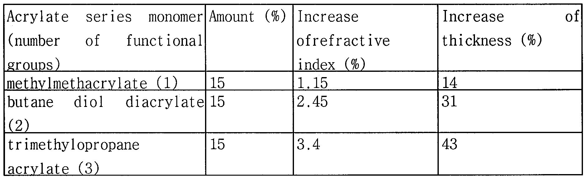
- Dopants can be classified in accordance with the number of acrylates of acrylate monomers, in other words, the number of functional groups into monomers with one functional group of butyl acrylate, ethyl hexyl acrylate, octyl/decyl acrylate, hydroxyalkyl acrylate, cyclohexyl acrylate and so on, monomers with two functional groups of butane diol diacrylate, butylene glycol dimethacrylate, hexanediol diacrylate, hexanediol dimethacrylate, tripropylene glycol diacrylate and so on, monomers with three functional groups of trimethylopropane triacrylate, trimethylopropane trimethacrylate, pentaerythritol triacrylate, glyceryl propoxylated triacryl
- the photoreactive monomer includes cinnamic acid and cinnamic esters series such as methyl cinnamate, ethyl cinnamate, vinyl cinnamate, allyl cinnamate, cinnamyl cinnamate and benzyl cinnamate, carboxylic acid cinnamyls series such as dicarboxylic acid cinnamyl and methacrylic acid cinnamyl, maleic acid series, maleic anhydride series, fumaric acid series, itaconic acid series, itaconic anhydride series, citraconic acid series, citraconic anhydride series and further methyl cinnamic acid, cinnamyl chloride, stilbene and methacrylate series.
- the present invention may use at least one selected from the photoactive monomers.
- a photochemical initiator monomer initiating the polymerization by forming a dimer in photoactive hybrid materials may be at least one monomer selected from the group consisting of benzoinether series, benzylketal series, dialkoxyacetonephenon series, hydroxyalkylphenon series and aminoalkylphenon series.
- FIG. 1 shows a process for fabricating a microlens by using a transparent photoimageable hybrid material doped on oligo-siloxane having a polymerizable organic functional group by a photoactive monomer.
- a layer (2) is coated by using a transparent photoimageable hybrid material doped on oligo-siloxane having a polymerizable organic functional group by a photoactive monomer.
- the substrate (1) and the photoimageable hybrid layer (2) can be formed by a general method. For example, a spin coating method capable of forming a layer having a uniform thickness can be adopted. Before coating a solution, the surface to be coated should be carefully cleansed. This cleansing process is useful in removing dust which might affect membranes or other external materials.
- a light (4) having a mask (3) with a desired shape and a specified wavelength is illuminated on the photoimageable hybrid layer (2) to perform a patterning process.
- the patterning process may be performed by using a laser instead of a mask.
- a desired micro-optical element pattern can be made by using a light corresponding to a wavelength where a photoinitiator reacts out of doped monomers.
- a wavelength corresponding to an ultraviolet light is used and a micro-optical element having a special shape can be fabricated in accordance with a desired shape.
- an organic monomer capable of participating in the reaction it is possible to use an organic monomer capable of participating in the reaction to include and fix oligo-siloxane having a polymerizable organic functional group in a cross link instead of a simple photoactive monomer.
- a light is partially illuminated on a layer to modify the structure of molecules in a dopant only in the portions where a light is illuminated.
- a polymerizable oligo-siloxane is coupled with monomers on the layer on which a light is illuminated, a monomer forms a dimer or a transition corresponding to the polymerization of a monomer occurs.
- the matrix, the amount of molecules and the structure of the doped monomer are different from those of the portion where a light is not illuminated, resulting in a selective concentration gradient of a photoactive monomer between the region where a light is illuminated and the region where a light is not illuminated.
- the photoactive monomers doped by continuously illuminating a differentiated light on a layer keep moving a light from a region where a light is illuminated to a region where a light is not illuminated.
- the monomers at the portion where a light is illuminated are coupled with oligo-siloxane or a dimer is formed from monomers or a transition corresponding to the polymerization of monomers keeps occurring, bringing about an adequate reduction or a complete reduction of the mobility and the volatility of doped photoactive monomers in a photoimageable hybrid material illuminated by a light.
- the photochemical initiator monomer in the photoimageable hybrid material forms two radicals as shown in (1) if a light is illuminated, and the formed radicals are coupled like (2) in case of one functional group, (3) in case of two functional groups, (4) in case of three functional groups and (5) in case of mixture of one functional group and two functional groups in accordance with the number of each functional group of acrylate series monomer capable of forming a polymer and having an organic mesh.
- the polymerizable acrylate series photoactive monomer in a matrix forms a chain arranged at random to be easily entangled through a photopolymerizat ion reaction at various points of the chain composing a photoimageable hybrid material. Accordingly, as a result of this reaction, the molecular structure of doped monomers and the structure of a matrix at the portion where a light is illuminated differ from those at the portion where a light is not illuminated. Thus, a photophoresis of monomers is performed to cause a polymerization with the matrix and various kinds of photo-reactions at portions where a light is illuminated.
- the molecular transition process as above can have various shapes and other kinds of reactions can be included besides the above molecular transition process.
- the diameter of a cross-section of a light in a layer and the direction of an axis can be controlled by changing the concentration of a light or the degree of an incident angle.
- c36> Therefore, if a wider linewidth is desired, a longer wavelength is preferable and the degree of an incident angle or the concentration of a beam may be reduced when the diameter of a light in a layer is increased.
- c37> The wavelength of an exposed beam does not have a clear effect on a polymerizable oligo-siloxane itself and should be selected to initiate the desired molecular transition in a photochemical initiator monomer.
- the selected specific wavelength is dependent on the components of oligo-siloxane having a specific monomer used as an initiating material and a polymerizable organic functional group in each case. Moreover, a wavelength which dissembles the components of a layer or has a harmful effect on the quality of the final elements should be excluded.
- a method for fabricating micro-optical elements through a photo- reaction shown as above may include a process for illuminating a light at the wavelength region with a greater transmittance with respect to a layer through a mask including the desired pattern of micro-optical elements.
- a technology using this mask is widely known and is a method to be adopted in fabricating a semiconductor device by using a photoresist in general. Furthermore, in case of using a laser, it is possible to directly illuminate a light without the mask.
- Electrons, ions and neutrons as well as a simple light source can be used in the step of illuminating a light.
- illuminating particles may be useful in obtaining a large space resolving power.
- the next step relates to the development of the pattern of micro- optical elements exposed to a light in a layer.
- the development can be performed by heating a layer in order to simply volatilize the doped monomer in the region which is not exposed to a light.
- This step leaves monomers participating in a photo-reaction at the portion where a light is illuminated to a layer and brings a result as follows.
- the thickness of a layer is decreased in the unexposed region by removing dopants unexposed to a light and a layer is exposed to a light so that the value of the refractive index is increased due to a photo-reaction between a matrix and a dopant and inside the dopant, resulting in relatively decreasing portions where a light is not illuminated and bringing about a soft change between the portion where a light is illuminated and the portion where a light is not illuminated.
- the highest temperature at the time of development can be limited by various physical and chemical characteristics of oligo-siloxane having photoactive monomers and polymerizable organic functional group used in the experiments. What should be considered is a glass transition temperature of oligo-si loxane having a polymerizable organic functional group and the diffusion caused by the temperature of dopants fixed in the oligo-si loxane having a polymerizable organic functional group and undesired chemical changes caused by the heat of materials. It is preferable that the development be performed at a temperature barely affecting the desired characteristics of the final element. For this reason, it is preferable that the photoactive monomer have a proper volatility so that the development occurs at a comparatively proper temperature.
- FIG. 1 (right) shows a process for fabricating diffraction gratings (4) having various sizes and shapes by a holographic interferometer using a laser (3) at the state (2) that a transparent photoimageable hybrid material doped by a photoactive monomer is coated to oligo-si loxane having a polymerizable organic functional group on the substrate (1).
- the mechanisms are the same as the tools in FIG. 1 (left).
- the micro-optical elements fabricated by a concentration gradient caused by the change of molecular structure raised by a photo-reaction of a photoimageable hybrid material and a photophoresis caused by the difference of a chemical potential have an advantage that a micro-optical element having a refractive index distribution as well as a soft volume in a device and other dielectric regions can be fabricated.
- the refractive index corresponding to the change of the cross-section of the magnitude of an exposed light obtains a soft and symmetrically crossing change on the basis of the axial direction.
- the concentration of fixedly bulky photoactive monomers with a high refractive index becomes the maximum by a photo-reaction and a photophoresis induced by the photo-reaction along an axis of an illuminating beam in general and is decreased gradually from the axis.
- the distribution of the thickness of a layer also becomes the maximum along the axis of an illuminating beam by a photophoresis in general and is decreased gradually from the axis.
- the thickness of a layer is in proportion to the concentration of monomers concerned in the photo-reaction.
- the photophoresis being a major equipment for directly fabricating a light by micro-optical elements made of a photoimageable hybrid material depends not only on the amount of an illuminated light including the magnitude of a light but also the thickness of a layer, the composition and the size of a predetermined region where a light is illuminated very sensitively. These variables are controlled to fabricate micro-optical elements with various shapes and to show a high efficiency in comparison with micro-optical elements fabricated by conventionally widely used methods through these features.
- the micro-optical elements fabricated by a photophoresis described as above were observed to be stable for more than one month at a room temperature and the fixed dopant is hardly diffused.
- the bulky and high refractive index dopant was used to increase the thickness of a selected region and a refractive index but it is easily understood by those skilled in the art that a low refractive index dopant can also move a light to a high refractive index matrix from the description of the present invention. If only the distribution of a thickness is to be obtained by a photophoresis, it is sufficient that the dopant and the matrix have the same refractive index.
- the above method is very useful in fabricating micro-optical elements having a regular change in a layer.
- microlens fabricated in the above-described way an array and micro-optical elements such as diffraction gratings having a periodic array are very useful in being applied as a very important interline-transfer element capable of improving fill factors in an image sensor of an optical communication element, CMOS and CCD.
- FIG. 1 is a process view of micro-optical elements according to the present invention.
- FIG. 2 shows a 3D picture of a surface profiler regarding the phenomenon of photophoresis of a micro-optical structure (circle (2a) and line (2b)) depending on the amount of an illuminated light of a photoimageable hybrid material observed by the present invention and a view showing the change of a height and a width regarding the phenomenon of photophoresis of a micro-optical structure (circle (2a) and line (2b)) depending on the amount of an illuminated light;
- FIG. 3 is a 3D picture of a microlens (3a) fabricated by the present invention and the surface profiler of the array (3b); 5> FIG.
- FIG. 4 is a view showing an image of a CCD camera with regard to a focal beam from the focal plane of the microlens (4b) fabricated by the present invention and the distribution (4a) of a focal beam of the microlens;6>
- FIG. 5 is a view showing the increase of a height of the pattern of a microlens array fabricated by the present invention in accordance with the change of the thickness of a photoimageable hybrid layer measured by a 3D surface profiler; 7> FIG.
- FIG. 6 is a view showing the change of a focal distance of a microlens array in accordance with the change of a height of the pattern of a microlens array fabricated by the present invention in accordance with the change of a thickness of a photoimageable hybrid layer; 8> FIG. 7 is a view showing the increase of a height of the pattern of a microlens array fabricated by the present invention in accordance with the change of the composition of a photoimageable hybrid layer measured by a 3D surface profiler;
- FIG. 8 shows the change of a focal distance of a microlens array in accordance with the change of the pattern of the height of the microlens array fabricated by the present invention in accordance with the change of the composition of a photoimageable hybrid layer! t ⁇ >
- FIG. 8 shows the change of a focal distance of a microlens array in accordance with the change of the pattern of the height of the microlens array fabricated by the present invention in accordance with the change of the composition of a photoimageable hybrid layer! t ⁇ >
- FIG. 9 is a view taken by an optical microscope of a diffraction grating fabricated by illuminating a direct laser by an holographic interferometer in accordance with the present invention without a mask (1-a Fresnel lens by a beam (9a), 2-2D linear diffraction grating by a beam (9b), 3-2D hexagonal diffraction grating by a beam (9c) and 4-2D rectangular diffraction grating by a beam (9d)); and
- FIG. 10 shows a CCD camera image regarding diffraction effects of diffraction gratings fabricated by illuminating a direct laser by an holographic interferometer in accordance with the present invention without a mask (Fresnel lens (10a), 2D linear diffraction grating by a beam (10b), 2D hexagonal diffraction grating by a beam (10c) and 2D rectangular diffraction grating (1Od)).
- Resnel lens (10a) 2D linear diffraction grating by a beam (10b)
- 2D hexagonal diffraction grating by a beam (10c)
- 2D rectangular diffraction grating (1Od)
- Methylmethacrylate is added by 15mol% of the entire alkoxide as a photoactive monomer for polymerization, and benzyldimethylketal (BDK) is added by 15mol% of the entire alkoxide as a photochemical initiator monomer capable of forming a dimer for polymerization and is stirred again to manufacture a photoimageable hybrid solution until the monomer is completely dissolved.
- BDK benzyldimethylketal
- methylmethacrylate added as a photoactive monomer for polymerization in the embodiment 1 is fixed to 15mol% and benzyldimethylketal (BDK) as a photochemical initiator monomer is mixed at a mole ratio with respect to the entire alkoxide shown in the below table 2, the same method as in the embodiment 1 was performed and a refractive index and the increased amount of a thickness were measured after a light is finally illuminated.
- BDK benzyldimethylketal
- a photoimageable hybrid solution including methylmethacrylate of 15mol% of the entire alkoxide and BDK of 15mol% added to the methacryl-fluoro- silica-zirconia-hybrid material gained in the embodiment 1 is coated on a wafer by a spin coater and a lamp is illuminated on a mask having the pattern of a microlens and an array structure and then it is heat-treated for 5 hours at 150 0 C.
- FIG. 3 is a 3D picture of a surface profiler of a microlens (3a) and an array (3b) fabricated by the method.
- FIG. 4 is an image of a CCD camera with respect to focal beams from a focal plane of the microlens (4a) and an array (4b) fabricated by the method.
- a photoimageable hybrid solution including methylmethacrylate of 15mol% of the entire alkoxide and BDK of 15mol% added to the methacryl-fluoro- silica-zirconia-hybrid material gained in the embodiment 1 is coated on a wafer by a spin coater. The coating is performed at a different speed to form a layer having a different thickness and a lamp is illuminated on a mask having the pattern of a microlens and the array structure and then it is o heat-treated for 5 hours at 150C.
- the increase of the height of a microlens array pattern in accordance with the thickness of a layer is measured by a 3D surface profiler and the change is shown in FIG. 5.
- the change of a focal length of a microlens array in accordance with the change of a height is shown in FIG. 6.
- a photoimageable hybrid solution mixing a photoactive monomer, methylmethacrylate fixed to 15mol% of the entire alkoxide in the methacryl- fluoro-silica-zirconia-hybrid material gained in the embodiment 1 and the photoinitiator BDK of 5%, 10%, 15% and 25% of the entire alkoxide is coated on a wafer by a spin coater.
- a lamp is illuminated on a mask having the pattern of a microlens and a array structure and then it is heat-treated for o 5 hours at 150C.
- the increase of the height of the microlens array pattern in accordance with the thickness of a layer is measured by a 3D surface profiler and the change is shown in FIG. 7.
- the change of a focal length of a microlens array in accordance with the change of a height is shown in FIG. 8.
- FIG. 9 is a view taken by an optical microscope of a diffraction grating fabricated by illuminating a direct light by an holographic interferometer in accordance with the present invention without a mask (1-a Fresnel lens by a beam (9a), 2-2D linear diffraction grating by a beam (9b), 3-2D hexagonal diffraction grating by a beam (9c) and 4-2D rectangular diffraction grating by a beam (9d)).
- FIG. 10 shows a CCD camera image regarding diffraction effects of diffraction gratings fabricated by illuminating a direct laser by an holographic interferometer in accordance with the present invention without a mask (Fresnel lens (10a), 2D linear diffraction grating by a beam (10b), 2D hexagonal diffraction grating by a beam (10c) and 2D rectangular diffraction grating (1Od)) .
- micro-optical elements can be simply fabricated without an etching process of a photolithography process requiring for a complicated process in fabricating micro-optical elements and further control optical characteristics of the micro-optical elements by the advantages in a progress.
Landscapes
- Physics & Mathematics (AREA)
- General Physics & Mathematics (AREA)
- Optics & Photonics (AREA)
- Engineering & Computer Science (AREA)
- Manufacturing & Machinery (AREA)
- Optical Integrated Circuits (AREA)
- Diffracting Gratings Or Hologram Optical Elements (AREA)
- Epoxy Resins (AREA)
- Macromonomer-Based Addition Polymer (AREA)
- Silicon Polymers (AREA)
Abstract
Description


Claims

Priority Applications (2)
| Application Number | Priority Date | Filing Date | Title |
|---|---|---|---|
| JP2009522698A JP4987980B2 (en) | 2006-08-02 | 2007-02-23 | Fabrication method of micro optical element using photographic development type hybrid material |
| US12/376,088 US20090311441A1 (en) | 2006-08-02 | 2007-02-23 | Fabrication method of micro-optical elements using photoimageable hybrid materials |
Applications Claiming Priority (2)
| Application Number | Priority Date | Filing Date | Title |
|---|---|---|---|
| KR10-2006-0073106 | 2006-08-02 | ||
| KR1020060073106A KR100786800B1 (en) | 2006-08-02 | 2006-08-02 | Manufacturing method of micro optical device using photo developing hybrid material |
Publications (1)
| Publication Number | Publication Date |
|---|---|
| WO2008016207A1 true WO2008016207A1 (en) | 2008-02-07 |
Family
ID=38997366
Family Applications (1)
| Application Number | Title | Priority Date | Filing Date |
|---|---|---|---|
| PCT/KR2007/000941 Ceased WO2008016207A1 (en) | 2006-08-02 | 2007-02-23 | Fabrication method of micro-optical elements using photoimageable hybrid materials |
Country Status (4)
| Country | Link |
|---|---|
| US (1) | US20090311441A1 (en) |
| JP (1) | JP4987980B2 (en) |
| KR (1) | KR100786800B1 (en) |
| WO (1) | WO2008016207A1 (en) |
Families Citing this family (4)
| Publication number | Priority date | Publication date | Assignee | Title |
|---|---|---|---|---|
| DE102013104600B4 (en) * | 2013-01-11 | 2019-10-17 | Fraunhofer-Gesellschaft zur Förderung der angewandten Forschung e.V. | Layers or three-dimensional moldings with two regions of different primary and / or secondary structure, process for the production of the molded article and materials for carrying out this process |
| US9535291B2 (en) * | 2013-09-24 | 2017-01-03 | Shenzhen China Star Optoelectronics Technology Co., Ltd | PSVA LCD panel and method for manufacturing the PSVA LCD panel |
| TWI559082B (en) | 2014-07-07 | 2016-11-21 | 財團法人工業技術研究院 | Biomass material and method for manufacturing the same and print circuit board |
| KR102309427B1 (en) * | 2018-09-27 | 2021-10-05 | 주식회사 엘지화학 | Holographic media |
Citations (3)
| Publication number | Priority date | Publication date | Assignee | Title |
|---|---|---|---|---|
| JP2002148822A (en) * | 2000-11-09 | 2002-05-22 | Nippon Synthetic Chem Ind Co Ltd:The | Manufacturing method of inorganic material microstructure |
| KR20030006896A (en) * | 2001-07-10 | 2003-01-23 | 학교법인 포항공과대학교 | Method for manufacturing a structure by using light source of high energy |
| US6764796B2 (en) * | 2001-06-27 | 2004-07-20 | University Of South Florida | Maskless photolithography using plasma displays |
Family Cites Families (10)
| Publication number | Priority date | Publication date | Assignee | Title |
|---|---|---|---|---|
| CA1294470C (en) * | 1986-07-26 | 1992-01-21 | Toshihiro Suzuki | Process for the production of optical elements |
| US5298366A (en) * | 1990-10-09 | 1994-03-29 | Brother Kogyo Kabushiki Kaisha | Method for producing a microlens array |
| JP3067114B2 (en) * | 1991-06-04 | 2000-07-17 | ソニー株式会社 | Micro lens formation method |
| US5286338A (en) * | 1993-03-01 | 1994-02-15 | At&T Bell Laboratories | Methods for making microlens arrays |
| TW581746B (en) * | 1999-11-12 | 2004-04-01 | Nippon Sheet Glass Co Ltd | Photosensitive composition, optical waveguide element and production process therefor |
| US6490390B1 (en) * | 2001-01-05 | 2002-12-03 | Phaethon Communications | Grating writing systems based on an acousto-optic element |
| JP2003029418A (en) * | 2001-07-10 | 2003-01-29 | Pohang Eng College | Manufacturing method for structure using high energy light source |
| JP2005508269A (en) * | 2001-11-02 | 2005-03-31 | エムイーエムエス・オプティカル・インコーポレイテッド | Method for manufacturing a micro-optical element from a gray scale etched master mold |
| US6858378B1 (en) | 2002-04-17 | 2005-02-22 | Sandia National Laboratories | Photoimageable composition |
| KR100705759B1 (en) * | 2005-01-17 | 2007-04-10 | 한국과학기술원 | Method for manufacturing flat plate multimode optical waveguide by direct optical patterning |
-
2006
- 2006-08-02 KR KR1020060073106A patent/KR100786800B1/en not_active Expired - Fee Related
-
2007
- 2007-02-23 US US12/376,088 patent/US20090311441A1/en not_active Abandoned
- 2007-02-23 JP JP2009522698A patent/JP4987980B2/en not_active Expired - Fee Related
- 2007-02-23 WO PCT/KR2007/000941 patent/WO2008016207A1/en not_active Ceased
Patent Citations (3)
| Publication number | Priority date | Publication date | Assignee | Title |
|---|---|---|---|---|
| JP2002148822A (en) * | 2000-11-09 | 2002-05-22 | Nippon Synthetic Chem Ind Co Ltd:The | Manufacturing method of inorganic material microstructure |
| US6764796B2 (en) * | 2001-06-27 | 2004-07-20 | University Of South Florida | Maskless photolithography using plasma displays |
| KR20030006896A (en) * | 2001-07-10 | 2003-01-23 | 학교법인 포항공과대학교 | Method for manufacturing a structure by using light source of high energy |
Also Published As
| Publication number | Publication date |
|---|---|
| JP4987980B2 (en) | 2012-08-01 |
| JP2009545766A (en) | 2009-12-24 |
| KR100786800B1 (en) | 2007-12-18 |
| US20090311441A1 (en) | 2009-12-17 |
Similar Documents
| Publication | Publication Date | Title |
|---|---|---|
| CA1294470C (en) | Process for the production of optical elements | |
| US8211625B2 (en) | Method of forming a locally periodic 3D structure with larger-scale variation in periodic properties and applications thereof | |
| US7067240B2 (en) | Gray scale fabrication method using a spin-on glass material and integrated optical designs produced therefrom | |
| WO2008016207A1 (en) | Fabrication method of micro-optical elements using photoimageable hybrid materials | |
| JP2009179678A (en) | Photocurable composition and cured film thereof | |
| JP2599497B2 (en) | Flat plastic optical waveguide | |
| JP3617846B2 (en) | Microlens / microlens array and manufacturing method thereof | |
| WO2001031401A1 (en) | Self-processing of diffractive optical components in hybrid sol-gel glasses | |
| JP2015038579A (en) | OPTICAL ELEMENT, OPTICAL SYSTEM, IMAGING DEVICE, OPTICAL DEVICE, MASTER, AND MANUFACTURING METHOD | |
| CN1558260A (en) | A method of fabricating waveguide Bragg gratings based on ultraviolet direct writing technology | |
| Kärkkäinen et al. | Direct photolithographic deforming of organomodified siloxane films for micro-optics fabrication | |
| KR100705759B1 (en) | Method for manufacturing flat plate multimode optical waveguide by direct optical patterning | |
| Park et al. | Photochemical reactions in fluorinated sol–gel hybrid materials doped with a photolocking agent for direct micropatterning | |
| KR100426959B1 (en) | Menufacturing Method for Planar Optical Waveguide | |
| JP2001356470A (en) | Method for producing three-dimensional structure using distributed density mask | |
| He et al. | A high-corrugation-rate self-Processing SiO 2--ZrO 2 hybrid sol-gel material for fabrication of microlens array | |
| Eisenberg et al. | New micro-optical devices for the IR based on three-component amorphous chalcogenide photoresists | |
| US7244369B2 (en) | Method for producing active or passive components on a polymer basis for integrated optical devices | |
| JP2002162747A (en) | Manufacturing method for three-dimensional structure by multistep exposure | |
| JP2002318319A (en) | Method for producing film having refractive index distribution | |
| JPH08286002A (en) | Production of microlens | |
| Kärkkäinen et al. | Photolithographic processing of hybrid glasses for microoptics | |
| JP2001356471A (en) | Distributed density mask and method for producing three- dimensional structure using the same | |
| JP2006003762A (en) | Optical element, optical element manufacturing method, and exposure apparatus | |
| Croutxe-Barghorn et al. | Microlens array fabrication through crosslinking photopolymerization |
Legal Events
| Date | Code | Title | Description |
|---|---|---|---|
| 121 | Ep: the epo has been informed by wipo that ep was designated in this application |
Ref document number: 07709078 Country of ref document: EP Kind code of ref document: A1 |
|
| DPE1 | Request for preliminary examination filed after expiration of 19th month from priority date (pct application filed from 20040101) | ||
| WWE | Wipo information: entry into national phase |
Ref document number: 2009522698 Country of ref document: JP |
|
| WWE | Wipo information: entry into national phase |
Ref document number: 12376088 Country of ref document: US |
|
| NENP | Non-entry into the national phase |
Ref country code: DE |
|
| NENP | Non-entry into the national phase |
Ref country code: RU |
|
| 122 | Ep: pct application non-entry in european phase |
Ref document number: 07709078 Country of ref document: EP Kind code of ref document: A1 |