WO2008014474A2 - Solver for hardware based computing - Google Patents
Solver for hardware based computing Download PDFInfo
- Publication number
- WO2008014474A2 WO2008014474A2 PCT/US2007/074630 US2007074630W WO2008014474A2 WO 2008014474 A2 WO2008014474 A2 WO 2008014474A2 US 2007074630 W US2007074630 W US 2007074630W WO 2008014474 A2 WO2008014474 A2 WO 2008014474A2
- Authority
- WO
- WIPO (PCT)
- Prior art keywords
- matrix
- power
- analog
- memory
- computation
- Prior art date
- Legal status (The legal status is an assumption and is not a legal conclusion. Google has not performed a legal analysis and makes no representation as to the accuracy of the status listed.)
- Ceased
Links
Classifications
-
- G—PHYSICS
- G06—COMPUTING OR CALCULATING; COUNTING
- G06F—ELECTRIC DIGITAL DATA PROCESSING
- G06F30/00—Computer-aided design [CAD]
- G06F30/30—Circuit design
- G06F30/32—Circuit design at the digital level
- G06F30/33—Design verification, e.g. functional simulation or model checking
- G06F30/3308—Design verification, e.g. functional simulation or model checking using simulation
- G06F30/331—Design verification, e.g. functional simulation or model checking using simulation with hardware acceleration, e.g. by using field programmable gate array [FPGA] or emulation
-
- G—PHYSICS
- G06—COMPUTING OR CALCULATING; COUNTING
- G06F—ELECTRIC DIGITAL DATA PROCESSING
- G06F17/00—Digital computing or data processing equipment or methods, specially adapted for specific functions
- G06F17/10—Complex mathematical operations
- G06F17/16—Matrix or vector computation, e.g. matrix-matrix or matrix-vector multiplication, matrix factorization
Definitions
- the current invention is related to a programmable linear algebraic solver for large sparse matrices based on a lower -upper triangular decomposition method to be used in a hardware computing environment. Furthermore, the present invention also relates to models for power system components and power systems.
- the bottleneck in Newton power flow iteration is the solution of a sparse system of linear equations, which is required for each iteration, and typically consumes 85% of the execution time in large-scale power systems [I].
- many related load flow computations are performed as part of contingency analysis. These multiple load flow computations can easily be performed in parallel. It remains desirable to speed up the computation of an individual load flow computation.
- Typical power flow computation is performed using general-puipose personal computing platforms based on processors such as the Intel Pentium IV®. High performance uniprocessor sparse linear solvers on these platforms utilize only roughly 1-4% of the floating-point throughput.
- Analog computation provides a viable alternative to traditional approaches. Among the advantages over traditional digital methods are physically realizable solutions and faster computation times. In order to make the analog method a viable tool in power system analysis, accurate models of power system components are required. A reconfigurable transmission line model is considered for a specific analog computation method. Traditional digital methods are expensive and slow in comparison to analog computers. The power flow solution is obtained almost instantaneously regardless of the number of components in the network with analog circuits. Essentially computation time is independent of network size. Effectively the solution is obtained as quickly as the system stabilizes. Experimentation has shown the ability to calculate solutions even faster than real time. In prior research, simulation time for a two-machine system was typically 104 times shorter than the real time simulated phenomena [101]. This is achieved by modeling generator dynamics for the purpose of transient stability evaluation.
- Emulation can be described as an act of a physical system imitating a real system.
- Emulation in this patent application therefore, is the representation of physical characteristics of a real life object (power system) using an electric circuit equivalent.
- the representational relationship could be mathematical, scaled, or both.
- the circuit equivalent representation has within it the model of a real system as well as a method of its solution.
- the speed of computation is as quick as the response of the circuit itself, which could be real time, faster or slower than real time depending on the parameter settings.
- the solution is continuous in time and amplitude.
- Simulation is an attempt to predict/replicate aspects of the behavior of a real system by creating an approximate (mathematical) model of it.
- Computer modeling for example by providing a special-purpose computer program, may do this.
- the program is composed of equations that describe the functional relationships within the real system.
- the resulting mathematical dynamics form an analog of the behavior of the real system with the results presented in the form of data.
- ABMs serve this purpose.
- the interior of a behavioral model is different in that it is implemented in terms of algebraic or differential equations rather than physical analog components.
- the focus is on the input/output relationship of the block.
- the fundamental advantage of the behavioral modeling technique in top-down designs is that the simulation can provide fast prediction of system performance.
- the approach helps to select proper architectures for circuit implementation and analyze tradeoffs at the early design stages.
- the transistor level simulation (bottom-up design) comparatively, can be very tedious and cumbersome especially for mixed-signal chips containing a large number of analog components. Under such circumstances, behavioral models enable designers to verify the complex system efficiently and result in fast system evaluation prior to embarking on full structural design and implementation.
- Static load flow analysis which is based on the power flow equations, is one method currently used by the industry. The problem is that suchanalyses solve using a sequential method, which makes the simulation process very slow in complex networks.
- the speed of the digital computer to solve for static load flow is greatly dependent on the size of the power system network.
- An alternative method to solve static load flow is using an analog computer to emulate the behavior of the power system, instead of using model equations to simulate the network.
- CMOS complementary metal oxide semiconductor
- SOI silicon-on-insulator
- CMOS devices have been scaled down continuously and the corresponding power consumption has also been decreased, which have triggered advances in the circuit design techniques for various designs and applications.
- the association between CMOS circuits and VLSI chips is becoming increasingly easier to implement.
- Fried et al. [302] proposed an approach using an analog VLSI chip for simulation of the behavior of power systems. Using an analog VLSI chip can be limited if the fabricated chip is only useful for one power system configuration.
- Gu et al. [303] presented a concept to add reconfigurable parameters using switches and analog voltages to change the system configuration and parameters.
- the system provides a substantially improved computing platform for solving computation intensive problems.
- One implementation includes Field Programmable Gate Arrays (FPGA) for the solution of sparse linear systems.
- FPGA Field Programmable Gate Arrays
- the system is implemented by a combination of downloadable core software and a dedicated hardware such as FPGA.
- the core software customizes the application of the FPGA for various computational analyses.
- a static transmission line is modeled for analog power flow computation. Operational transconductance amplifiers in the model provide reconfigurability of transmission line parameters via transconductance gain.
- Analog Behavioral Models are implemented for use in analog emulation engines for large-scale power system computation.
- ABMs are applied for model verification and validation prior to full structural design and implementation.
- a generator model using analog circuits is developed for load flow emulation for power system analysis to reduce computation time.
- the generator model may include reconfigurable parameters using operational transconductance amplifiers (OTAs).
- OTAs operational transconductance amplifiers
- the circuit module is used with other reconfigurable circuits, i.e., transmission lines and loads.
- Figure 1 is a diagram illustrating SYMAMD elimination row histogram.
- Figure 2 is a diagram illustrating the architecture of one preferred embodiment according to the current invention.
- Figure 3 is a diagram illustrating the pivot search logic block of one preferred embodiment according to the current invention.
- Figure 4 is a diagram illustrating the update pivot column/row read logic block of one preferred embodiment according to the current invention.
- Figure 5 is a diagram illustrating the update unit of one preferred embodiment according to the current invention.
- Figure 6 is a graph illustrating the relation between the increased speed and the number of update units according to the current invention.
- Figure 7 is a graph illustrating the relative solve times for a single update unit according to the current invention.
- Figure 8 is a graph illustrating the relative solve times for sixteen update units according to the current invention.
- Figure 9 is a graph illustrating the LU hardware performance relative to a Pentium
- Figure 10 is a circuit diagram illustrating a DC network emulation for a three-bus power system.
- Figure 11 is a diagram illustrating a lossy transmission line model.
- Figure 12 is a diagram illustrating a lossless transmission line model.
- Figure 13 is a diagram illustrating an ideal operational transconductance amplifier (OTA).
- OTA operational transconductance amplifier
- Figure 14 is a diagram illustrating a double ended OTA transmission line model.
- Figure 15 is a diagram illustrating a potentiometer relationship to OTA model.
- Figure 16 is a diagram illustrating PSpice schematic for bias current control.
- Figure 17 is a graph plotting bias current vs. bias voltage.
- Figure 18 is a graph plotting theoretical and simulated resistance vs. bias voltage.
- Figure 19 is a graph plotting line current vs. line voltage.
- Figure 20 is a graph plotting line current vs. line voltage linear region.
- Figure 21 is a graph illustrating effective resistance of line model.
- Figure 22 is a graph plotting effective resistance of line model vs. line voltage.
- Figure 23 is a graph plotting hardware and spice effective resistance vs. bias voltage.
- Figure 24 is a graph plotting HW line current vs. line voltage for various bias currents.
- Figure 25 is a graph illustrating line current linearity.
- Figure 26 is a graph plotting HW resistance vs. line voltage.
- Figure 27 is a diagram illustrating a three-bus power system topology.
- Figure 28 is a diagram illustrating a three-bus prototype board.
- Figure 29 is a diagram illustrating an emulation circuit setup.
- Figure 30 is a diagram illustrating a power world power flow solution.
- Figure 31 is a diagram illustrating analog and ABM sine shaper.
- Figure 32 is a time line of hardware technology.
- Figure 33 illustrates complex computation methodology
- Figure 34 is a diagram illustrating a complex computation implementation.
- Figure 35 is a diagram illustrating generator real power computation methodology.
- Figure 36 is a diagram illustrating computationally feasible bus voltage.
- Figure 37 illustrates variable representation in analog emulator.
- Figure 38 is a diagram illustrating a power system emulator hardware setup.
- Figure 39 is a diagram illustrating a classical generator model.
- Figure 40 is a block diagram illustrating a swing equation functional block.
- Figure 41 is a block diagram illustrating generator model functions.
- Figure 42 is a diagram illustrating a single-machine CMON analog emulator.
- Figures 43a-b show diagrams illustrating results of power system and analog emulator.
- Figure 44 is a diagram illustrating results of analog emulator with offset corrections.
- FPGA Programmable Gate Arrays
- one aspect of the present invention relates to hardware for the direct solution of sparse linear systems.
- the hardware design takes advantage of properties of the matrices arising in the specific computation obtained from a detailed analysis of actual systems.
- Field programmable gate arrays are reconfigurable logic devices that allow users to configure device operation through software.
- Arrays of programmable logic blocks, combined with programmable I/O blocks, and programmable interconnects form the underlying reconfigurable fabric for FPGAs.
- Software code typically written in a hardware description language (HDL) such as VHDL or Verilog, is mapped to these devices allowing the user to specify the functionality of the FPGA.
- FPGAs can be programmed multiple times, unlike other programmable logic devices (PLD), which can only be programmed once.
- PLD programmable logic devices
- ASIC application specific integrated circuits
- FPGA device densities are in the millions for logic gates with clock rates of 500 MHz for synthesized logic (see www.xilinx.com). Beyond increases in logic density, the addition of high performance embedded arithmetic units, large amounts of embedded memory, high speed embedded processor cores, and high speed I/O has allowed FPGAs to grow beyond just simple prototyping devices. FPGAs can outperform high-end personal computers [3]. Based on synthesis results, a high-end FPGA such as a Xilinx Virtex-4TM contains enough embedded multiplier and logic resources to support over 40 high-speed single precision floating-point multipliers operating at 300 MHz. Unlike personal computer processors, FPGAs have the advantage of being able to be mapped to the desired application, rather than being designed to perform well across a wide range of applications. This allows the greatest amount of utilization of the available resources on the FPGA.
- the present invention will be exemplified based on power flow computation. However, the present invention is applicable to other types of complex computations as well.
- the Jacobian, J of the power system, is a large highly sparse matrix (very few non-zero entries), which while not symmetric has a symmetric pattern of non-zero elements.
- ⁇ x is a vector of the change in the voltage magnitude and phase angle for the current iteration.
- f(x) is a vector representing the real and imaginary power mismatch.
- Direct linear solvers perform Gaussian Elimination, which is performed by decomposing tithe matrix A into Lower (L) and Upper (U) triangular factors, followed by forward and backward elimination to solve for the unknowns.
- Dense matrix linear solvers are not as efficient as specialized solvers designed for sparse matrices. These solvers do not compute the non-zero entries. However, they suffer from a phenomenon known as fill-in. Fill-in of a sparse matrix during LU decomposition arises when a previously zero entry in the matrix becomes non-zero during the elimination process. Large amounts of fill-in will degrade the performance of sparse solvers by incieasing the number of mathematical operations required for the LU decomposition. By using an appropriate elimination order, the amount of fill-in can be dramatically reduced [5]. Selecting the optimal ordering is an NP complete problem [6]. However, effective heuristics are known that work quite well for the matrices in load flow computation. In addition, sparse matrix solvers do not share the regular computational pattern of dense matrix solvers and as a consequence there is significant overhead in accessing and maintaining data structures that utilize the sparse data.
- Benchmark System and Properties An in-depth analysis of the elimination process was performed using four power systems of various sizes. Two of the systems, the 1648 Bus and 7917 Bus systems, were obtained from the PSS/E data collection, and the other two systems, the 10279 Bus and 26829 Bus systems, were obtained from power systems used by PJM Interconnect. The purpose of the analysis was to obtain features of the systems arising in typical power system computation that could be utilized in the design of special-purpose hardware. In addition, the systems were also used to benchmark the proposed hardware and compare it against a state- of-the art software solution. Table 1 summarizes the number of branches and number of non- zeros (NNZ) in the Ybus matrices and the size and number of non-zeros of typical Jacobian matrices for the benchmark systems.
- NZ non- zeros
- the number of floating-point subtractions (FSUB), multiplications (FMUL), divisions (FDIV), and the growth of the matrices as a result of fill-in were collected for the Jacobians and are summarized in Tables2 and 3 This information was used to project performance and estimate storage requirements for the resulting L and U factors.
- the MATLAB functions COLAMD and SYMAMD were used to determine elimination ordering.
- the number of fill- ins is equal to the number of non-zeros in the L and U factors compared to the Jacobian.
- SYMAMD utilizes the symmetric structure of the non-zeros in the Jacobian and provides a substantial reduction in fill-in and arithmetic operations.
- the performance is proportional to the number of floating point operations (FLOPs) divided by the throughput of the floatingpoint hardware.
- FLOPs floating point operations
- MFLOPs million floating point operations per second
- a sparse matrix storage scheme is much more space efficient than dense storage when dealing with matrices of large size, but very few non-zero values.
- Row compressed storage is a common method used by sparse solvers [7]. This scheme stores the non-zero values of a sparse matrix by a set of row vectors, one vector containing non-zero values and the other containing the corresponding column indices.
- the amount of storage required to store the L and U factors is approximately 7 MB for the largest test system, solved using the SYMAMD pre- permutation. This amount of storage is well within the space available on off the shelf memory chips (www.micron.com).
- the pattern of non-zero elements that arise during the elimination process was analyzed in order to estimate the available parallelism, intermediate storage requirements, and potential for data reuse.
- Table 4 shows the average number of non-zero elements in the rows and columns of the matrix as the elimination process proceeds. It is used as an estimate for the amount of row or column parallelism (separate rows can be updated in parallel) that can be achieved by utilizing multiple FPUs. Observe that the reduced fill-in obtained by SYMAMD leads to reduced parallelism.
- the amount of resources on an FPGA can support the number of floating-point units required to achieve maximal parallelism.
- Figure 1 shows the distribution of the number of non-zero entries in the rows that occur during the LU factorization for the 1648 Bus system. The x-axis is the number of non- zeros and the vertical bars indicate the number of rows with that many non-zero entries. The bulk of the elimination rows are at or below the average. This histogram is representative of all of the row and column results for both COLAMD and SYMAMD across all four benchmark systems.
- the maximum number of non-zero elements in a row determines the size of buffers that store rows.
- Table 5 shows the maximum NNZ in a row for the entire row as well as the portion of the row used during elimination (Table 5).
- 19K bits of storage is required for the largest elimination row of the 26829 Bus system.
- Today's FPGAs contain thousands of Kbits of high speed embedded memory, which is enough to buffer hundreds of rows or columns.
- the comparison system used in the benchmarks is a 2.60 GHz Pentium IV® computer running Mandrake Linux 9.2TM.
- Software was compiled using gcc v3.3.1 (flags -03 -fPIC) and utilizing ATLAS CBLAS libraries.
- Three high-end sparse solvers were tested, UMFPACK (Un-Symmetric Multi-Frontal Package) [8], SupeiLU
- the proposed hardware implements the Gaussian elimination with partial pivoting LU factorization algorithm shown below:
- FIG. 2 shows a block diagram of the overall design of one preferred embodiment according to the current invention.
- the Pivot Search Logic, Update Pivot Column/Row Read Logic, and Update Unit Logic blocks each perform a portion of the overall LU algorithm, with control and memory access handled by the other two blocks on the FPGA.
- the memory hierarchy to which the processing logic connects consists of a write-back row-cache implemented in a fast random-access memory such as SRAM, as well as a larger block of SDRAM which is used to store the matrix rows which do not fit into the row cache.
- the colmap is a redundant column-wise array of the indices of non-zeio elements in the matrix. The purpose of the colmap is to increase the efficiency of the pivot search.
- the minimum size of the row cache is equal to the amount of memory required to store the largest sub-matrix update, which is proportional to the product of the maximum number of non-zero elements in an elimination row and the maximum number of non-zero elements in an elimination column.
- a cache of this size insures that all row writes for a given sub-matrix update will be cache hits and will occur at cache speed, since all row misses will only occur during pivot search insuring row availability during sub-matrix update.
- the parameters to calculate the amount of cache required was extracted as previously described under Elimination Details.
- the cache row size, SDRAM row size, and colmap tow size exceed the maximum counts, which were extracted during the initial matrix profiling. This insures that the memories will have enough space to store the worst case, however, this also means that there will be inefficiencies in the storage for the typical case.
- the facilities required to maintain row pivoting information which is implemented by lookup tables and memory pointers, which keep track of the row to memory mappings for the compressed row storage format.
- An additional table is used to keep track of elimination progress to avoid reading row values that are not part of the sub-matrix update, i.e., elements that have already been eliminated.
- the size of these lookup tables scales linearly with matrix size. Depending on the size of the matrices to be solved and the available on-chip resources, these tables can be stored in embedded memory on-chip or if they are larger, in off-chip memory.
- the pivot search logic block performs the pivot search prior to each sub-matrix elimination step.
- a memory read of the column map followed by indexing logic creates the indices for the pivot column.
- the column map stores the physical address of rows in a particular column. The physical address must then be translated to the corresponding matrix row number. Since the colmap may contain rows which have already been eliminated, index rejection logic is required to select the appropriate indices.
- the physical addresses corresponding to these indices are then used to access the values from memory. The values are compared sequentially as they arrive to obtain the absolute maximum value and index. This value is stored in a register as the pivot element.
- the physical indices, virtual indices, and floating-point values for the pivot column are also stored in registers to be used by the pivot column update logic.
- the minimum amount of memory required for these registers is equal to the product of the largest elimination column in the matrix and the amount of storage for two indices and one value.
- the update pivot column/row read logic block performs normalization prior to elimination in parallel with the pivot row requested from memory.
- the pivot index, pivot value, and pivot column are from the pivot search logic ( Figure 3). After the pivot row is completely read from memory into buffers, and at least one of the update column entries has been created the next part of the elimination logic can proceed. Since the design utilizes a floating-point divider with a pipeline rate of 1 per clock cycle, all of the remaining divides will complete before they are requested by the update unit logic.
- the update row indices and values, and the normalized update column indices (physical and virtual) and values are stored in registers. The minimum size of this register space is equal to the product of the maximum elimination row in the matrix and the amount of space required to store three indices and two values.
- Update Unit Logic performs the remaining computations required during the elimination step.
- the processing logic can support multiple update units operating in parallel. Each update unit is tasked with completing the elimination for a single row of the sub-matrix to be updated. Each update unit contains a floating-point multiplier and adder to perform the required arithmetic as well as other logic that operates on the column indices.
- the computational logic operates in parallel with the memory and indexing logic to maximize utilization of all of the logic units.
- the number of update units that can fit on the FPGA is limited by the amount of on-chip embedded memory available, the number of multipliers available, and also the available logic resources. A high end FPGA has enough resources to support over 16 of these units.
- the merge logic maintains the row order and also determines if the multiplier output is a fill-in, an update, and also determines if the sub-matrix row element should be copied into the new row. If an entry is a fill-in, the colmap table is updated in the background to reflect the newly added index. Updates that result in a zero value are not pruned from the colmap and they are also stored in the row result. All logic in the update unit is pipelined for maximum throughput. Once the front end of the update unit has completed processing, it can request the next available row to be operated on in order to eliminate idle logic cycles. After all of the pending row eliminations for the current sub-matrix update have been completed, the next pivot search can begin. Hardware Performance Model
- a program was written in C, to project the performance of the hardware design. This program performs the elimination in the same fashion as the hardware would, and operates on an input file that contains the power system Jacobian matrix.
- the number of clock cycles the hardware requires to obtain the L and U factors is accumulated based on the latency and throughput of the processing logic and memory hierarchy. This cycle count allows us to compute the computation time based on clock speed.
- the memory model used for accessing SDRAM utilized three parameters to model the average behavior of a SDRAM memory: verall latency, burst read length, and latency between bursts.
- the model parameter was latency from request to data output.
- the only parameter for the floating-point hardware is the pipeline length, which affects the latency of results. All units were assumed to have a pipeline rate of 1 per clock cycle, even the floating-point division hardware. Extending the model to multiple instances of update unit logic was done by simulating round-robin service for each update unit by the memory hierarchy assuming a proportional increase in bandwidth.
- the clock rate for memory and logic was assumed to be synchronous at 200 MHz. This system clock rate was chosen because this was the maximum clock rate reported by VHDL synthesis for our floating-point units.
- Table 8 shows the projected performance of the proposed LU hardware architecture based on the four test power systems using the SYMAMD pre-permutation at a clock rate of 200 MHz.
- the simulated hardware performance achieves approximately 80% of the performance predicted by opcount.
- the projected performance using COLAMD (not shown) is less than SYMAMD, regardless of the number of update units used.
- Figure 6 shows the relative speedup of the LU hardware by increasing the number of update units. Scaling to even four update units does not net an equivalent speedup in overall solve time. The reason for this is apparent in Figures 7 and 8.
- Figures 7 and 8 show the relative time spent in the three portions of the LU hardware solution.
- Figures 7 and 8 show the relative time spent in the three portions of the LU hardware solution.
- Figure 7 For the single update unit configuration ( Figure 7), the majority of the time is spent performing the matrix update. Roughly a quarter of the time is spent searching for the pivot value.
- a figure 8 show that as the number of update units increases, the amount of time spent during pivot searching begins to dominate the overall solve time
- Figure 9 shows the predicted performance ratio of performance of the LU hardware at 200 MHz to the Pentium IV® benchmark system. This data predicts a speedup over the Pentium IV® of a factor of 10 with only 4 update units and approximately 15 with 16 units.
- a limiting factor is the time for pivot search. Eliminating or reducing the pivot search time will result in additional gains in performance. Such improvement may be obtained by overlapping the next pivot search with the current update, however, this is limited by the amount of reuse in rows from one elimination step to the next.
- BDB Bordered Diagonal Block
- a DC emulation power flow method has been proposed in [102] and is reviewed here for an understanding of the application of the line model in this invention.
- This approach utilizes multiple DC networks as shown in Figure 10.
- the power system is broken up into three main components: generators, transmission lines, and loads.
- the generators are shown as voltage sources.
- This form of DC emulation is possible due to the fact that the emulation is executed in rectangular coordinates.
- the generators excite the network with real (Re ⁇ E g ⁇ ) and imaginary (Im ⁇ E g ⁇ )voltage components and the states (voltages and currents) of these networks provide the steady-state power flow solution.
- the transmission line components in this emulation scheme are purely resistive and the imaginary resistor values are dependant upon operating frequency. By modeling as fixed resistors the frequency is assumed to be constant.
- R 11 and X 11 are the resistance and reactance of a line between buses i and j.
- the same approach is used for lossless transmission lines.
- the transmission line resistances are neglected as shown in Figure 12.
- the topology is similar to Figure 10 with the exclusion of networks 1 and 4. Similarly, it is solved by omitting the excluded networks.
- the transmission lines were modeled as resistors in the DC emulation shown previously for both lossy and lossless lines. Actual use of resistors would requiie manual intervention to configure and alter the analog system. In order to overcome this problem, a remotely reconfigurable OTA based variable resistor was developed to model the lines.
- the transconductance gain (g m ) of an OTA is controllable through an external source over a wide range, allowing remote reconfigurability.
- the basic OTA only consists of a few current minors resulting in a small and relatively low-cost device. They are also readily used in VLSI design. Due to its versatility, the OTA is one of the most important building blocks of analog VLSI circuits [105] and can be highly accurate if used properly.
- OTAs Some of the pitfalls of OTAs are their sensitivity to temperature and saturation effects but there are methods to correct these [106, 107].
- the principle operation of an OTA is a voltage controlled current source (VCCS).
- Figure 13 shows an ideal OTA.
- the amplifier has a differential voltage input and a current output.
- the current output is related to the differential input through a transconductance gain (g m ) controllable through an external source. Ideally the output would be: where v m is the differential input voltage.
- FIG. 14 illustrates a double-ended OTA transmission line model [108]. This line model has three terminals similar to a variable resistor.
- the two inputs (V 1 , V 2 ) mimic terminals of a resistor and the i abc is the biasing current used to control the resistance of the model similar to the wiper on a potentiometer.
- the terminal relationship to a potentiometer is shown in Figure 15.
- the effective resistance, Reff, of the OTA model is defined as the resistance seen between terminals Vi and V 2 .
- Reff is governed directly by Ohm's law through the line voltage (Vii n e) and the line current (Ii, ne ).
- resistors R and R A The sizing of resistors R and R A along with the range of transconductance gain will determine the behavior of the circuit. With appropriate resistors and wide control over gain a very large range of effective resistance is obtainable.
- the limitations of the circuit are related to properties of OTAs. The limitations, operation and controllability were analyzed through PSPice simulations and hardware testing.
- Simulation A LMl 3700 dual OTA was used for the simulations in PSPice.
- Various simulations were run to validate and characterize the line model. Controllability, resistance variance and circuit limitations were analyzed.
- the first simulation dealt with controlling the circuit through the bias current. Applying a current source is not as simple and easily controllable in comparison to a voltage source.
- the simulation using the circuit in Figure 16 uses a voltage source (V a t> c ) behind impedance (R a bc) to drive the bias current.
- a voltage sweep was performed on V abC and the corresponding bias current produced was measured.
- the relationship between bias voltage and i a t, c is differ entiable until i a b c approached zero as shown in Figure 17.
- the gain in (9) is not linear, typical applications linearize g m around an operating point.
- the differential input of the OTA is limited within very small range to ensure accuracy of this linear approximation.
- the LMl 3700 OTA gain is also a hyperbolic function although it improves the linearity through the use of linearizing diodes. These diodes allow a larger swing of input voltage while maintaining linear behavior.
- the gain for this chip, factoring in the diodes, is approximated by (10) for a differential input voltage in the range of ⁇ 50 mV. This gain can directly control the effective resistance in (7).
- V ⁇ 26mV and D is a diode linearization constant.
- the saturation of the circuit is dependant on two factors: the bias current and the throughput current.
- the effective resistance has a variance of ⁇ 2% with throughput current 40% or less of the bias current. Complete saturation occurs when the throughput current is equal to the bias current.
- Further examination of Figure 20 reveals an offset in the circuit behavior.
- the output of the circuit is nonzero when no voltage is applied to the input (one of the line terminals). This is problematic as the effective resistance of the circuit governed by Ohm's law is nonlinear.
- the computation of this resistance is shown in Figure 21 and exhibits anomalous behavior.
- the offset current present at the output of the OTA is almost entirely caused by the internal offset voltage of the OTA.
- This can be modeled in a similar manner as offset voltages of traditional op-amps. Specifically, a voltage source (v Of t) at the input of the device is amplified to the output producing the offset (i Off set). For an OTA, this is quantified by (11).
- the effective resistance is plotted against line voltage in Figure 26.
- the variance of the effective resistance was less than 1%. This is an accurate range for operation of this model.
- the line model becomes less accurate, saturation effects become more severe, as the line current magnitude approaches the bias current magnitude.
- the linear range for this model defined by ⁇ 1% variance, is quantified by the following relationship:
- the line voltage can be any magnitude as long as the relationship in (12) is maintained. This is advantageous as the linear operating voltage range has been significantly increased from a basic open loop OTA with the use of feedback. This will allow easy measurement of the bus voltages in an emulation network.
- the results from both simulation and hardware were very similar and verity the operation, control and linear operating conditions of the proposed OTA based transmission line model. A three-bus prototype was constructed and tested based on these results.
- a network module prototype of a three-bus power system was built based on the proposed transmission line model. This design was incorporated on a single circuit board containing the transmission line components of the four networks as shown in Figure 10. It is suitable for both lossy and lossless models shown in Figures 11 and 12, respectively.
- the main purpose of this prototype was to validate the transmission line model application in the previously proposed DC emulation power flow technique [102], The configuration of the power system is shown in Figure 27.
- the power system consists of one load, two generators and three transmission lines (A, B, C).
- Four independent networks containing three OTA based variable resistors were used in this emulation. The combination of these networks constitutes the complete transmission line model.
- the circuit board contains only the line models with terminals to attach generator and load models.
- the complete circuit board is shown in Figure 28.
- the lines (A, B, C) are highlighted in the picture to show the relationship to the power system along with the labeling of the four networks in relation to Figure 10.
- the input terminals for generators, loads, and power supply are also shown. For simplistic operation with fewer power supplies, all the bias currents are driven by the +15 volt supply.
- the network module was configured for power flow emulation.
- DC voltage sources were used as generators (values were obtained from a computed steady-state power flow solution) and the load was an OTA based constant current source. This is shown in Figure 29. While this setup requires the prior knowledge of the generator bus voltages, the appropriate voltage on the load bus corresponding to the correct load currents is sufficient to verify the functionality of the network module.
- the results were compared to results from the Power World® software package [111].
- the network module was configured per the lossless system in Power World® shown in Figure 30. Table 9 shows the results, load bus voltage in per unit, from both the hardware (offset corrected) and the software computation.
- the transmission line model presented is sufficient for lossy and lossless line models for use in the DC emulation static power flow technique mentioned.
- the overall model consists of multiple OTA based variable resistor circuits.
- the shortcomings of the hardware prototype, such as linear range, accuracy and device offsets, are mostly due to the current OTA technology. This can be overcome with further development of better performing
- simulation and/or emulation are used when dealing with large-scale power systems. They make it possible to do essential assessment in power system dispatch, operation, security and stability. Different simulation/emulation tools today are built for different applications like transient stability analysis, fault analysis, power flow studies, operational planning, etc.
- ABMs are used to make flexible descriptions of electronic components or complex building block in teims of transfer function or lookup tables. In order words, a mathematical relationship is used to model a circuit segment so one will not need to design the segment component by component.
- Figure 31 shows a sine shaper which is a device that outputs sine value of its input signal.
- Figure 31 The left side of Figure 31 is a modified Barry Gilbert sine shaper [203] built component by component using analog devices, and the right side of Figure 31 is an ABM sine shaper [201]. The only similarity between the two is that they both take the same input signal and produce the same output.
- One aspect of the invention employs transient stability analysis with the advantages of shorter computation time than current digital simulations and smaller size and cost than discrete analog emulators.
- One of the main disadvantages of this method is the limited accuracy due to the implementation of the analog VLSI chip.
- ABSMs Analog Behavioral Models
- Power system core computation methodology implemented in the design of analog emulation goes through three major steps. These steps are illustrated in Figure 32. The assumptions made and detailed processes are discussed in [21 1] and [202], respectively.
- Step 1 Calculating complex voltage out of generator
- the generator block solves the swing equation (dynamic) with resulting power angle, ⁇ .
- the power angle combines with desired voltage magnitude to give a complex voltage out of a generator.
- Step II Calculating currents in the network
- Step III Computation of generator real power and swing equation update
- the real power out of each generator in the system is calculated as the real part of the product of generator terminal voltage and complex conjugate of the generator current:
- the swing equation describes the dynamics of a generator. Its input is a mechanical power from a prime mover and which is assumed constant. The output of a generator is an electrical power, which changes in accordance with the state of the network.
- the swing equation is a second order differential equation and its solution is the power angle of the generator. The power angle combines with generator internal voltage to constantly update the generator terminal voltage and hence the generator current.
- Figure 35 describes the continuous cycle of power system core computation.
- Figure 36 describes the DC-network equivalent of a real power system bus and conditions for its implementation. Analyzing a sample power system and considering an arbitrary bus k with its complex voltage values, there are 4 networks with 4 buses K 1 , K ⁇ , K m ,and K IV as equivalents. For feasible bus voltages, the following conditions must be satisfied:
- Scale factors are constants that relate the values of the variables on the emulator to the values of the variables in the real system under study.
- Cases studied which include 3-bus, 6-bus and 14-bus lossy and lossless power systems, were implemented using ABMs of PSpice.
- ABMs substitute real analog circuit implementation of the mathematical equations and scaled relationship that describe the states of the power system cases and emulate their behaviors. Power flow tests ere conducted on each of the cases. Similar cases were tested on industrial grade numerical simulation software, PowerWoild® v9.1 [212] and Powei System Simulation for Engineering® (PSS/E) v.28.1 [213], for benchmarking.
- PSS/E Powei System Simulation for Engineering®
- the proposed circuit is based largely upon the classical generator model. This section presents a short review of the basics behind the generator model developed and scaling of the model to an appropriate analog circuit.
- the classical generator model that will be used for this example consists of a voltage source behind an impedance, where Yz 0 represents the
- Ez ⁇ denotes the internal generator voltage and angle
- Z representing the transient reactance of the generator 'dX.
- the generator consisting of these elements can be seen in Figure 39.
- the representation of the electrical output power will need to be applied directly into the swing equation for the calculation of the electrical angle.
- the functionality of the swing equation as seen in the block diagram in Figure 40 will provide us with a layout for the generator model that will be presented in the following section. With many different models representing the generator available, we will use the classical model while neglecting damping. This will simplify the non-linear dynamics of the classical generator without significantly reducing the precision of the model [305]. With these assumptions, the swing equation (17) will reduce to only the difference between the mechanical input power and the electrical output power. After factoring in the generator inertia coefficient and taking two integration steps of the angular acceleration, the solution of the electrical power angle can be calculated in the following form:
- the time scaling parametei is for the computation speedup of the emulator while the scaling of parameter space is for the electrical angle to be represented as voltage in the circuit.
- ⁇ a constant which will represent a computational speedup of ⁇ times faster than the real-time system.
- This factor is directly proportional to the real time of the power system, t, for a given simulation time of the analog emulator, T.
- the time scale factor needs to be squared because of the second order nature involved in the dynamics of the classical generator model.
- a collaborating factor that may influence the choice of the time scale is that the error in the integration may be accentuated by long emulation times.
- Another scaling procedure is actual parameter scaling of the electrical angle to voltage.
- the next step of modeling addresses the concept of reconfigurability in the generator model,
- the actual analog circuit representing the generator needs to incorporate a programmable analog device into model to obtain controllable behaviors of the power system.
- the operational transconductance amplifier OTA will be used because of its ability to control its gain by an external current (or voltage).
- the OTA has the basic properties of a voltage-controlled current source (VCCS) and the output current is obtained by: a product of the transconductance parameter and the differential input voltage.
- the transconductance, gm can be increased or decreased as a function of the input voltage by varying the amplifier bias current, labc, according to this equation: as a gain and is dependent on a non-linear device constant, p and the amplifier bias current as seen in (23) [306].
- the desirable gain of an OTA would always be constant, with a linear input and output relationship. Since this is not the case, measures will need to be considered because of the errors that will result from the non-linear transconductance of the OTA.
- the analog circuit developed to solve the swing equation of the generator will consist of two first -order integrators built using OTAs [306].
- the output of the double integration process is voltage representing the electrical angle and is calculated in the following manner analogous to (21).
- the I e (V) represents electrical power which is dependent on the electrical angle.
- the components Ci and C 2 are the values of the integration capacitor needed in the first and second integrators, respectively.
- the transconductance parameters, g ml and g m2 are the gains of the first and second OTAs in the double integration process. These values can be reconfigured using the amplifier bias currents to correspond to various generator characteristics and a given range of speedup times.
- a functional block diagram of the generator behavioral model is made up of voltage-controlled current sources (VCCS), current-controlled voltage source (CCVS), amplifiers, integrators, and various other components that determine the electrical output power of the generator.
- Figure 41 represents the block diagram of the analog behavioral model of the generator.
- the current, I m is used to quantify mechanical power.
- the difference between this current and I e is used as the input into the double integrator scaled as voltage.
- the voltage output of the double integrator is equivalent to the electrical angle given by (21).
- electrical power output is dependent on generator terminal voltage and current.
- P e ( ⁇ ) it will be scaled to a corresponding cu ⁇ ent value, Ie(V), and the process updates itself until a possible stable steady-state solution is attained.
- appropriate CMOS devices must be selected. Consideiations used for selection include minimal device power consumption, suitable device operating ranges, and transconductance.
- the devices selected for this model will use commercial off-the-shelf (COTS) CMOS components including the National Semiconductor LMl 3700 OTA [307] and the Analog Devices AD639 Trigonometric Converter [308].
- COTS commercial off-the-shelf
- the calculation of the steady-state solution of the electrical angle of the generator can be found by solving the instantaneous generator power for the system,
- the analog circuit for the single-machine power system consisted of four OTAs, a trigonometric converter, and resistors and capacitors as seen in Figure 42.
- the controllable gains were calculated in order to fit the circuit to the power system, which was dependent on the selection of the resistor and capacitors in the circuit.
- the selection of the resistor values were needed to scale the parameters to proper voltage levels for the OTAs to function within their linear operating range.
- the capacitor selection determined the integration time of the circuit.
- the gain representing the maximum electrical power output, P e , m a ⁇ , is transformed into the maximum current gain parameter A, which is equivalent to I e,max -
- the maximum allowable current parameter will be controlled through the gain of an OTA, g mA . This can be changed for different power system parameters in the following manner from equations (24) and (26).
- the two gains of the OTAs within the double integrator are considered identical to one another.
- the gains can be characterized in terms of the following:
- the power system parameters are directly associated with a controllable gain parameter.
- the controllable gain is directly associated with the generator inertia constant and the scaling parameters defined in equations (20) and (21). This allows for a completely reconf ⁇ gurable classical generator model that provides computational speedup for conventional digital methods.
- the reconfigurable classical generator model has been tested in a single-machine power system.
- the results of the simulation shown are from the circuit emulator of Figure 42 using PSpice and will be compared to simulation results obtained using PSpice Analog Behavior Models (ABM). This comparison is validated from previous work [310] conducted using Analog Behavior Models of sample power systems, where the results obtained compared rather favorably with traditional load flow solvers such as PSS/E and PowerWorld®.
- the power system parameters and the associated circuit parameters based on the previous equations for the simulation example are listed in Table 14.
- the mechanical input power is fixed constant at 0.5 per unit (p.u.) while the emulator solves for a steady-state solution.
- the results of the actual angular solution are different with a large degree of error.
- the ABM power system model solved for the angular solution of 22.89°
- the OTA analog emulator model solved for the angular solution of 27.79°.
- the difference between the two results has an error of approximately 21-22%. Since the steady- state calculation of the actual electrical angle using equation (26) results in an angle of 22.89°, the analog emulator seems to produce the error. Since the present invention focuses on the study of load flow analysis of power systems, and not the intricate design of electronic devices, the offset correction method that will be applied to this example will be the post-processing of the data to correct for the offset of the devices.
- the present invention is applicable to many different areas. One method would be the introduction of initial conditions on the integrator to start at a value that may be closer to a desired stable solution. Also, more complicated models could be developed to expand this model to include damping and higher order generator models.
- the present invention is useful for modeling of power systems and power system components. This can be used for fail-safe planning, as well as for operations planning.
- the present system is flexible enough to allow long- term planning over the life of the system, as well as to facilitate short-term operations planning for operating the system as little as 24 hours to 7 days ahead of time. This is possible since the present invention uses the hardware up to about 10 times more efficiently than all-purpose computing platforms.
- the hardware of the present invention including the FPGA and related components, are flexible enough to be customized for a variety of different calculations.
- the present invention has been exemplified for power system planning, it is generally applicable to other systems requiring complex computations as well.
Landscapes
- Engineering & Computer Science (AREA)
- Physics & Mathematics (AREA)
- General Physics & Mathematics (AREA)
- Mathematical Physics (AREA)
- Theoretical Computer Science (AREA)
- Data Mining & Analysis (AREA)
- Pure & Applied Mathematics (AREA)
- Computational Mathematics (AREA)
- Mathematical Analysis (AREA)
- Mathematical Optimization (AREA)
- Computer Hardware Design (AREA)
- General Engineering & Computer Science (AREA)
- Algebra (AREA)
- Computing Systems (AREA)
- Databases & Information Systems (AREA)
- Software Systems (AREA)
- Evolutionary Computation (AREA)
- Geometry (AREA)
- Supply And Distribution Of Alternating Current (AREA)
- Design And Manufacture Of Integrated Circuits (AREA)
- Amplifiers (AREA)
- Management, Administration, Business Operations System, And Electronic Commerce (AREA)
Abstract
FuIl-AC load flow constitutes a core computation in power system analysis. The present invention provides a performance gain with a hardware implementation of a sparse-linear solver using a Field Programmable Gate Array (FPGA). The invention also relates to the design, simulation, and hardware verification of a static transmission line model for analog power flow computation. Operational transconductance amplifiers are employed in the model based on a previously proposed DC emulation technique of power flow computation, and provide reconfigurability of transmission line parameters via transconductance gain. The invention also uses Analog Behavioral Models (ABMs) in an efficient strategy for designing analog emulation engines for large-scale power system computation. Results of PSpice simulations of these emulation circuits are compared with industrial grade numerical simulations for validation. The application is also concerned with the development of a generator model using analog circuits for load flow emulation for power system analysis to reduce computation time. The generator model includes reconfigurable parameters using operational transconductance amplifiers (OTAs). The circuit module is used with other reconfigurable circuits, i.e., transmission lines and loads.
Description
SOLVER FOR HARDWARE BASED COMPUTING
BACKGROUND OF THE INVENTION 1. Field of the Invention The current invention is related to a programmable linear algebraic solver for large sparse matrices based on a lower -upper triangular decomposition method to be used in a hardware computing environment. Furthermore, the present invention also relates to models for power system components and power systems.
2. Brief Description of the Prior Art
Currently, power flow computation for large power systems is time intensive. The calculations are non-linear in nature and lengthy iteration schemes are the currently preferred solution. This presents a problem as many assumptions and simplifications are required to solve the equations in a timely manner. In addition, expansion of the power grid, increasing necessity and complexity of contingency studies and introduction of economic analysis are demanding further computational burden. Traditional digital methods are too slow to solve the aforementioned demands quickly. This affects the security, reliability and market operation of power systems. Ideally a real-time computation tool is preferable, specifically in market activities and operation. In power flow computations, sparse linear solvers are used to calculate the update vector for the Jacob ian matrix at each iterative step during Newton-Raphson iteration for load flow solution. The bottleneck in Newton power flow iteration is the solution of a sparse system of linear equations, which is required for each iteration, and typically consumes 85% of the execution time in large-scale power systems [I]. In practice, many related load flow computations are performed as part of contingency analysis. These multiple load flow computations can easily be performed in parallel. It remains desirable to speed up the computation of an individual load flow computation. Typical power flow computation is performed using general-puipose personal computing platforms based on processors such as the Intel Pentium IV®. High performance uniprocessor sparse linear solvers on these platforms utilize only roughly 1-4% of the floating-point throughput. Attempts have also been made xo increase performance through the use of cluster computing [1], however, due to the irregular data flow and small granularity of the problem these methods do not scale very well.
Analog computation provides a viable alternative to traditional approaches. Among the advantages over traditional digital methods are physically realizable solutions and faster computation times. In order to make the analog method a viable tool in power system analysis, accurate models of power system components are required. A reconfigurable transmission line model is considered for a specific analog computation method. Traditional digital methods are expensive and slow in comparison to analog computers. The power flow solution is obtained almost instantaneously regardless of the number of components in the network with analog circuits. Essentially computation time is independent of network size. Effectively the solution is obtained as quickly as the system stabilizes. Experimentation has shown the ability to calculate solutions even faster than real time. In prior research, simulation time for a two-machine system was typically 104 times shorter than the real time simulated phenomena [101]. This is achieved by modeling generator dynamics for the purpose of transient stability evaluation.
The modeling and design of analog components is one obstacle that must be overcome. The solutions will only be as accurate as the models and measurements will allow. Without clearly defined valid models for power system components, the analog computational method will never be realized. In addition, these models also must cater towards computational speed. Specifically, in power system operation, multiple runs and contingencies are required to be executed extremely quickly. A priority for these analog models is to yield valid solutions while allowing fast reconfigurability.
An efficient strategy for designing analog emulation engines for large scale power system computation may be provided through the use of Analog Behavioral Models (ABMs) of PSpice [201]. Emulation can be described as an act of a physical system imitating a real system. Emulation in this patent application, therefore, is the representation of physical characteristics of a real life object (power system) using an electric circuit equivalent. The representational relationship could be mathematical, scaled, or both. The circuit equivalent representation has within it the model of a real system as well as a method of its solution. The speed of computation is as quick as the response of the circuit itself, which could be real time, faster or slower than real time depending on the parameter settings. The solution is continuous in time and amplitude.
Simulation on the other hand is an attempt to predict/replicate aspects of the behavior of a real system by creating an approximate (mathematical) model of it. Computer modeling, for example by providing a special-purpose computer program, may do this. The program is composed of equations that describe the functional relationships within the real system.
When the program is run, the resulting mathematical dynamics form an analog of the behavior of the real system with the results presented in the form of data.
The need to emulate/simulate large and complex mixed-signal systems has prompted the development of high-level circuit representations for analog components; ABMs serve this purpose. The interior of a behavioral model, however, is different in that it is implemented in terms of algebraic or differential equations rather than physical analog components. In order words, in a behavioral model, the focus is on the input/output relationship of the block. The fundamental advantage of the behavioral modeling technique in top-down designs is that the simulation can provide fast prediction of system performance. The approach helps to select proper architectures for circuit implementation and analyze tradeoffs at the early design stages. The transistor level simulation (bottom-up design), comparatively, can be very tedious and cumbersome especially for mixed-signal chips containing a large number of analog components. Under such circumstances, behavioral models enable designers to verify the complex system efficiently and result in fast system evaluation prior to embarking on full structural design and implementation.
Static load flow analysis, which is based on the power flow equations, is one method currently used by the industry. The problem is that suchanalyses solve using a sequential method, which makes the simulation process very slow in complex networks. The speed of the digital computer to solve for static load flow is greatly dependent on the size of the power system network. An alternative method to solve static load flow is using an analog computer to emulate the behavior of the power system, instead of using model equations to simulate the network.
In the past two decades, silicon-on-insulator (SOI) complementary metal oxide semiconductor (CMOS) technology has become a major technology for integrating VLSI systems using a low-supply voltage [301]. Along with the progress in the CMOS technology, CMOS devices have been scaled down continuously and the corresponding power consumption has also been decreased, which have triggered advances in the circuit design techniques for various designs and applications. The association between CMOS circuits and VLSI chips is becoming increasingly easier to implement. With these advances, Fried et al. [302], proposed an approach using an analog VLSI chip for simulation of the behavior of power systems. Using an analog VLSI chip can be limited if the fabricated chip is only useful for one power system configuration. Gu et al. [303], presented a concept to add reconfigurable parameters using switches and analog voltages to change the system configuration and parameters.
SUMMARY OF THE INVENTION
According to one aspect of the current invention, the system provides a substantially improved computing platform for solving computation intensive problems. One implementation includes Field Programmable Gate Arrays (FPGA) for the solution of sparse linear systems.
According to a second aspect of the current invention, the system is implemented by a combination of downloadable core software and a dedicated hardware such as FPGA. The core software customizes the application of the FPGA for various computational analyses. According to a third aspect of the current invention, a static transmission line is modeled for analog power flow computation. Operational transconductance amplifiers in the model provide reconfigurability of transmission line parameters via transconductance gain.
According to a fourth aspect of the current invention, Analog Behavioral Models (ABMs) are implemented for use in analog emulation engines for large-scale power system computation. ABMs are applied for model verification and validation prior to full structural design and implementation.
According to a fifth aspect of the current invention, a generator model using analog circuits is developed for load flow emulation for power system analysis to reduce computation time. The generator model may include reconfigurable parameters using operational transconductance amplifiers (OTAs). The circuit module is used with other reconfigurable circuits, i.e., transmission lines and loads.
BRIEF DESCRIPTION OF THE DRAWINGS
Figure 1 is a diagram illustrating SYMAMD elimination row histogram. Figure 2 is a diagram illustrating the architecture of one preferred embodiment according to the current invention.
Figure 3 is a diagram illustrating the pivot search logic block of one preferred embodiment according to the current invention.
Figure 4 is a diagram illustrating the update pivot column/row read logic block of one preferred embodiment according to the current invention.
Figure 5 is a diagram illustrating the update unit of one preferred embodiment according to the current invention.
Figure 6 is a graph illustrating the relation between the increased speed and the number of update units according to the current invention.
Figure 7 is a graph illustrating the relative solve times for a single update unit according to the current invention.
Figure 8 is a graph illustrating the relative solve times for sixteen update units according to the current invention. Figure 9 is a graph illustrating the LU hardware performance relative to a Pentium
IV® processsor.
Figure 10 is a circuit diagram illustrating a DC network emulation for a three-bus power system.
Figure 11 is a diagram illustrating a lossy transmission line model. Figure 12 is a diagram illustrating a lossless transmission line model.
Figure 13 is a diagram illustrating an ideal operational transconductance amplifier (OTA).
Figure 14 is a diagram illustrating a double ended OTA transmission line model.
Figure 15 is a diagram illustrating a potentiometer relationship to OTA model. Figure 16 is a diagram illustrating PSpice schematic for bias current control.
Figure 17 is a graph plotting bias current vs. bias voltage.
Figure 18 is a graph plotting theoretical and simulated resistance vs. bias voltage.
Figure 19 is a graph plotting line current vs. line voltage.
Figure 20 is a graph plotting line current vs. line voltage linear region. Figure 21 is a graph illustrating effective resistance of line model.
Figure 22 is a graph plotting effective resistance of line model vs. line voltage.
Figure 23 is a graph plotting hardware and spice effective resistance vs. bias voltage.
Figure 24 is a graph plotting HW line current vs. line voltage for various bias currents.
Figure 25 is a graph illustrating line current linearity. Figure 26 is a graph plotting HW resistance vs. line voltage.
Figure 27 is a diagram illustrating a three-bus power system topology.
Figure 28 is a diagram illustrating a three-bus prototype board.
Figure 29 is a diagram illustrating an emulation circuit setup.
Figure 30 is a diagram illustrating a power world power flow solution. Figure 31 is a diagram illustrating analog and ABM sine shaper.
Figure 32 is a time line of hardware technology.
Figure 33 illustrates complex computation methodology.
Figure 34 is a diagram illustrating a complex computation implementation.
Figure 35 is a diagram illustrating generator real power computation methodology.
Figure 36 is a diagram illustrating computationally feasible bus voltage.
Figure 37 illustrates variable representation in analog emulator.
Figure 38 is a diagram illustrating a power system emulator hardware setup.
Figure 39 is a diagram illustrating a classical generator model. Figure 40 is a block diagram illustrating a swing equation functional block.
Figure 41 is a block diagram illustrating generator model functions.
Figure 42 is a diagram illustrating a single-machine CMON analog emulator.
Figures 43a-b show diagrams illustrating results of power system and analog emulator.
Figure 44 is a diagram illustrating results of analog emulator with offset corrections.
DETAILED DESCRIPTION OF THE PREFERRED EMBODIMENTS
In the current invention, application-specific hardware is employed to reduce the computation time for the solution of the sparse linear systems arising in complex computations. The use of special-purpose hardware reduces the overhead costs, better utilizes floating-point hardware, and provides fine-grained parallelism. The use of Field
Programmable Gate Arrays (FPGA) provides a convenient platform to design and implement such hardware. By building hardware that is specifically designed to solve the sparse matrices found in complex calculations, such as power system calculations, rather than utilizing general-purpose processors and parallel processing, the present invention significantly improves the efficiency of the linear solver and hence reduces the computing time compared to traditional platforms.
Thus, one aspect of the present invention relates to hardware for the direct solution of sparse linear systems. The hardware design takes advantage of properties of the matrices arising in the specific computation obtained from a detailed analysis of actual systems.
Overview of FPGA Technology
Field programmable gate arrays (FPGA) are reconfigurable logic devices that allow users to configure device operation through software. Arrays of programmable logic blocks, combined with programmable I/O blocks, and programmable interconnects form the underlying reconfigurable fabric for FPGAs. Software code, typically written in a hardware description language (HDL) such as VHDL or Verilog, is mapped to these devices allowing the user to specify the functionality of the FPGA. FPGAs can be programmed multiple times, unlike other programmable logic devices (PLD), which can only be programmed once. In addition, unlike application specific integrated circuits (ASIC), there is not a long lead time in
between design and testing since the designer does not have to wait for masks and then for manufacturing to return a part for test. The user simply compiles the design for the desired FPGA and then programs the device.
FPGA device densities are in the millions for logic gates with clock rates of 500 MHz for synthesized logic (see www.xilinx.com). Beyond increases in logic density, the addition of high performance embedded arithmetic units, large amounts of embedded memory, high speed embedded processor cores, and high speed I/O has allowed FPGAs to grow beyond just simple prototyping devices. FPGAs can outperform high-end personal computers [3]. Based on synthesis results, a high-end FPGA such as a Xilinx Virtex-4™ contains enough embedded multiplier and logic resources to support over 40 high-speed single precision floating-point multipliers operating at 300 MHz. Unlike personal computer processors, FPGAs have the advantage of being able to be mapped to the desired application, rather than being designed to perform well across a wide range of applications. This allows the greatest amount of utilization of the available resources on the FPGA.
Overview of Power Flow by Newton's Method
The present invention will be exemplified based on power flow computation. However, the present invention is applicable to other types of complex computations as well.
Power flow solution via Newton's method [4] involves iterating the following equation:
-JΔx = f(x) (1)

Until f(x) = 0 is satisfied. The Jacobian, J, of the power system, is a large highly sparse matrix (very few non-zero entries), which while not symmetric has a symmetric pattern of non-zero elements. Δx is a vector of the change in the voltage magnitude and phase angle for the current iteration. And f(x) is a vector representing the real and imaginary power mismatch. The above set of equations are of the form Ax = B, which can be solved using a direct linear solver. Direct linear solvers perform Gaussian Elimination, which is performed by decomposing tithe matrix A into Lower (L) and Upper (U) triangular factors, followed by forward and backward elimination to solve for the unknowns. Dense matrix linear solvers are not as efficient as specialized solvers designed for sparse matrices. These solvers do not compute the non-zero entries. However, they suffer from a phenomenon known as fill-in. Fill-in of a sparse matrix during LU decomposition arises when a previously zero entry in the matrix becomes non-zero during the elimination process. Large amounts of fill-in will degrade the performance of sparse solvers by
incieasing the number of mathematical operations required for the LU decomposition. By using an appropriate elimination order, the amount of fill-in can be dramatically reduced [5]. Selecting the optimal ordering is an NP complete problem [6]. However, effective heuristics are known that work quite well for the matrices in load flow computation. In addition, sparse matrix solvers do not share the regular computational pattern of dense matrix solvers and as a consequence there is significant overhead in accessing and maintaining data structures that utilize the sparse data.
Benchmark System and Properties An in-depth analysis of the elimination process was performed using four power systems of various sizes. Two of the systems, the 1648 Bus and 7917 Bus systems, were obtained from the PSS/E data collection, and the other two systems, the 10279 Bus and 26829 Bus systems, were obtained from power systems used by PJM Interconnect. The purpose of the analysis was to obtain features of the systems arising in typical power system computation that could be utilized in the design of special-purpose hardware. In addition, the systems were also used to benchmark the proposed hardware and compare it against a state- of-the art software solution. Table 1 summarizes the number of branches and number of non- zeros (NNZ) in the Ybus matrices and the size and number of non-zeros of typical Jacobian matrices for the benchmark systems.

Operation Count (opcounts) and FiIl-In Study
The number of floating-point subtractions (FSUB), multiplications (FMUL), divisions (FDIV), and the growth of the matrices as a result of fill-in were collected for the Jacobians and are summarized in Tables2 and 3 This information was used to project performance and estimate storage requirements for the resulting L and U factors. The MATLAB functions COLAMD and SYMAMD were used to determine elimination ordering. The number of fill- ins is equal to the number of non-zeros in the L and U factors compared to the Jacobian. SYMAMD utilizes the symmetric structure of the non-zeros in the Jacobian and provides a substantial reduction in fill-in and arithmetic operations.


Given a floating point throughput limited calculation, the performance is proportional to the number of floating point operations (FLOPs) divided by the throughput of the floatingpoint hardware. Based on the flop counts and a throughput of 200 million floating point
operations per second (MFLOPs), the projected solve time for the largest system is approximately 0.11 seconds, solved using the SYMAMD pre-permutation.
The storage requirement for the L and U factors is proportional to the number of nonzero elements for a non-restoring design, where the original inputs are overwritten by the resulting solution. A sparse matrix storage scheme is much more space efficient than dense storage when dealing with matrices of large size, but very few non-zero values. Row compressed storage is a common method used by sparse solvers [7]. This scheme stores the non-zero values of a sparse matrix by a set of row vectors, one vector containing non-zero values and the other containing the corresponding column indices. Assuming 32-bit indices and 32-bit values for the matrix entries, the amount of storage required to store the L and U factors is approximately 7 MB for the largest test system, solved using the SYMAMD pre- permutation. This amount of storage is well within the space available on off the shelf memory chips (www.micron.com).
Elimination Details
The pattern of non-zero elements that arise during the elimination process was analyzed in order to estimate the available parallelism, intermediate storage requirements, and potential for data reuse.
Table 4 shows the average number of non-zero elements in the rows and columns of the matrix as the elimination process proceeds. It is used as an estimate for the amount of row or column parallelism (separate rows can be updated in parallel) that can be achieved by utilizing multiple FPUs. Observe that the reduced fill-in obtained by SYMAMD leads to reduced parallelism. The amount of resources on an FPGA can support the number of floating-point units required to achieve maximal parallelism. Figure 1 shows the distribution of the number of non-zero entries in the rows that occur during the LU factorization for the 1648 Bus system. The x-axis is the number of non- zeros and the vertical bars indicate the number of rows with that many non-zero entries. The bulk of the elimination rows are at or below the average. This histogram is representative of all of the row and column results for both COLAMD and SYMAMD across all four benchmark systems.
The maximum number of non-zero elements in a row determines the size of buffers that store rows. Table 5 shows the maximum NNZ in a row for the entire row as well as the portion of the row used during elimination (Table 5). Using 32-bit indices and 32-bit floating point values, 19K bits of storage is required for the largest elimination row of the 26829 Bus
system. Today's FPGAs contain thousands of Kbits of high speed embedded memory, which is enough to buffer hundreds of rows or columns.


The amount of reuse between subsequent elimination rows impacts the potential efficiency of a memory hierarchy. Rows that are reused from one iteration to the next can be cached and a iow not used in the previous iteration can be prefetched. Rows reused in subsequent eliminations do not allow pivot search to occur in parallel with computation during elimination since some values being calculated are necessary for the next pivot search. Table 6 shows that slightly more than half of the rows are reused between subsequent iteiations.
Table 6: Mean Percentage of Non-Zero Row Elements Reused between Successive Elimination Rows

Software Performance
The comparison system used in the benchmarks is a 2.60 GHz Pentium IV® computer running Mandrake Linux 9.2™. Software was compiled using gcc v3.3.1 (flags -03 -fPIC) and utilizing ATLAS CBLAS libraries. Three high-end sparse solvers were tested, UMFPACK (Un-Symmetric Multi-Frontal Package) [8], SupeiLU
(http://www.cs.beikeley.edu/~demmel/SuperLU.html), and WSMP (Watson Sparse Matrix Package: http://www-users.cs.umn.edu/~agupta/wsmp.html). Of the three solvers, UMFPACK gave the best results on all four systems. The numerical solve time, floating point operations per second, and floating point efficiency of the comparison system were gathered using the power system matrices. Despite the 2.6 GHz clock speed and impressive computational power of the Pentium IV® benchmark system, even the highest performance software was only able to utilize a fraction of the total available floating-point resources.

The proposed hardware implements the Gaussian elimination with partial pivoting LU factorization algorithm shown below:
For each column in the matrix loop Search column for pivot element
Pivot if necessary Normalize pivot column Update remaining portion of matrix:
Multiply to form sub-matrix update Update value or create fill-in
End loop
In order to maximize performance, the design of the LU hardware focused on maintaining regular computation and memory access patterns that are parallelized wherever possible. Figure 2 shows a block diagram of the overall design of one preferred embodiment according to the current invention. The Pivot Search Logic, Update Pivot Column/Row Read Logic, and Update Unit Logic blocks each perform a portion of the overall LU algorithm, with control and memory access handled by the other two blocks on the FPGA. The memory hierarchy to which the processing logic connects, consists of a write-back row-cache implemented in a fast random-access memory such as SRAM, as well as a larger block of SDRAM which is used to store the matrix rows which do not fit into the row cache. Our design makes full use of Dual-Ported SRAM memories which allow memory reads and writes to occur simultaneously. An additional bank of random-access memory is also required to store the colmap. The colmap is a redundant column-wise array of the indices of non-zeio elements in the matrix. The purpose of the colmap is to increase the efficiency of the pivot search.
The minimum size of the row cache is equal to the amount of memory required to store the largest sub-matrix update, which is proportional to the product of the maximum number of non-zero elements in an elimination row and the maximum number of non-zero elements in an elimination column. A cache of this size insures that all row writes for a given sub-matrix update will be cache hits and will occur at cache speed, since all row misses will only occur during pivot search insuring row availability during sub-matrix update. The parameters to calculate the amount of cache required was extracted as previously described under Elimination Details.
- I i-
For the initial design, the cache row size, SDRAM row size, and colmap tow size exceed the maximum counts, which were extracted during the initial matrix profiling. This insures that the memories will have enough space to store the worst case, however, this also means that there will be inefficiencies in the storage for the typical case. Not shown in the hardware diagrams are the facilities required to maintain row pivoting information, which is implemented by lookup tables and memory pointers, which keep track of the row to memory mappings for the compressed row storage format. An additional table is used to keep track of elimination progress to avoid reading row values that are not part of the sub-matrix update, i.e., elements that have already been eliminated. The size of these lookup tables scales linearly with matrix size. Depending on the size of the matrices to be solved and the available on-chip resources, these tables can be stored in embedded memory on-chip or if they are larger, in off-chip memory.
Pivot Search Logic Now refeiring to Figure 3, the pivot search logic block performs the pivot search prior to each sub-matrix elimination step. A memory read of the column map followed by indexing logic creates the indices for the pivot column. The column map stores the physical address of rows in a particular column. The physical address must then be translated to the corresponding matrix row number. Since the colmap may contain rows which have already been eliminated, index rejection logic is required to select the appropriate indices. The physical addresses corresponding to these indices are then used to access the values from memory. The values are compared sequentially as they arrive to obtain the absolute maximum value and index. This value is stored in a register as the pivot element. The physical indices, virtual indices, and floating-point values for the pivot column are also stored in registers to be used by the pivot column update logic. The minimum amount of memory required for these registers is equal to the product of the largest elimination column in the matrix and the amount of storage for two indices and one value. After pivoting is complete, a background update is sent to lookup tables (not shown) to maintain the correct row and address mappings for future translations.
Update Pivot Column/Row Read Logic
Now refeπing to Figure 4, the update pivot column/row read logic block performs normalization prior to elimination in parallel with the pivot row requested from memory. The pivot index, pivot value, and pivot column are from the pivot search logic (Figure 3). After the pivot row is completely read from memory into buffers, and at least one of the update column entries has been created the next part of the elimination logic can proceed. Since the design utilizes a floating-point divider with a pipeline rate of 1 per clock cycle, all of the remaining divides will complete before they are requested by the update unit logic. The update row indices and values, and the normalized update column indices (physical and virtual) and values are stored in registers. The minimum size of this register space is equal to the product of the maximum elimination row in the matrix and the amount of space required to store three indices and two values.
Update Unit Logic Now referring to Figure 5, the update unit logic performs the remaining computations required during the elimination step. In this design, the processing logic can support multiple update units operating in parallel. Each update unit is tasked with completing the elimination for a single row of the sub-matrix to be updated. Each update unit contains a floating-point multiplier and adder to perform the required arithmetic as well as other logic that operates on the column indices. The computational logic operates in parallel with the memory and indexing logic to maximize utilization of all of the logic units. The number of update units that can fit on the FPGA is limited by the amount of on-chip embedded memory available, the number of multipliers available, and also the available logic resources. A high end FPGA has enough resources to support over 16 of these units. The merge logic maintains the row order and also determines if the multiplier output is a fill-in, an update, and also determines if the sub-matrix row element should be copied into the new row. If an entry is a fill-in, the colmap table is updated in the background to reflect the newly added index. Updates that result in a zero value are not pruned from the colmap and they are also stored in the row result. All logic in the update unit is pipelined for maximum throughput. Once the front end of the update unit has completed processing, it can request the next available row to be operated on in order to eliminate idle logic cycles. After all of the pending row eliminations for the current sub-matrix update have been completed, the next pivot search can begin.
Hardware Performance Model
A program was written in C, to project the performance of the hardware design. This program performs the elimination in the same fashion as the hardware would, and operates on an input file that contains the power system Jacobian matrix. The number of clock cycles the hardware requires to obtain the L and U factors is accumulated based on the latency and throughput of the processing logic and memory hierarchy. This cycle count allows us to compute the computation time based on clock speed.

The memory model used for accessing SDRAM utilized three parameters to model the average behavior of a SDRAM memory: verall latency, burst read length, and latency between bursts. For the SRAM and embedded memories the model parameter was latency from request to data output. The only parameter for the floating-point hardware is the pipeline length, which affects the latency of results. All units were assumed to have a pipeline rate of 1 per clock cycle, even the floating-point division hardware. Extending the model to multiple instances of update unit logic was done by simulating round-robin service for each update unit by the memory hierarchy assuming a proportional increase in bandwidth. The clock rate for memory and logic was assumed to be synchronous at 200 MHz. This system clock rate was chosen because this was the maximum clock rate reported by VHDL synthesis for our floating-point units.
Table 8 shows the projected performance of the proposed LU hardware architecture based on the four test power systems using the SYMAMD pre-permutation at a clock rate of 200 MHz. The simulated hardware performance achieves approximately 80% of the performance predicted by opcount. The projected performance using COLAMD (not shown) is less than SYMAMD, regardless of the number of update units used. Figure 6 shows the relative speedup of the LU hardware by increasing the number of update units. Scaling to
even four update units does not net an equivalent speedup in overall solve time. The reason for this is apparent in Figures 7 and 8.
Figures 7 and 8 show the relative time spent in the three portions of the LU hardware solution. For the single update unit configuration (Figure 7), the majority of the time is spent performing the matrix update. Roughly a quarter of the time is spent searching for the pivot value. A figure 8 show that as the number of update units increases, the amount of time spent during pivot searching begins to dominate the overall solve time
Figure 9 shows the predicted performance ratio of performance of the LU hardware at 200 MHz to the Pentium IV® benchmark system. This data predicts a speedup over the Pentium IV® of a factor of 10 with only 4 update units and approximately 15 with 16 units.
These results show that special-purpose hardware implemented using existing FPGA provides a 1Ox or higher performance increase, compared to software solutions using state- of-the-art sparse linear solvers, for the LU decompositions that arise in typical power flow computations. The speedup is obtained by utilizing special-purpose hardware to reduce the overhead to access and maintain data structures for sparse matrices and the use of finegrained parallelism which performs multiple row updates in parallel. The reduction in overhead dramatically improves the utilization of the floating-point units as compared to software solutions on general-purpose processors.
A limiting factor is the time for pivot search. Eliminating or reducing the pivot search time will result in additional gains in performance. Such improvement may be obtained by overlapping the next pivot search with the current update, however, this is limited by the amount of reuse in rows from one elimination step to the next. The use of other approaches such as the Bordered Diagonal Block (BDB) technique may provide additional parallelism.
Analog Power Flow Method
A DC emulation power flow method has been proposed in [102] and is reviewed here for an understanding of the application of the line model in this invention. This approach utilizes multiple DC networks as shown in Figure 10. The power system is broken up into three main components: generators, transmission lines, and loads. The generators are shown as voltage sources. This form of DC emulation is possible due to the fact that the emulation is executed in rectangular coordinates. The generators excite the network with real (Re{E g }) and imaginary (Im{E g })voltage components and the states (voltages and currents) of these networks provide the steady-state power flow solution. The transmission line components in
this emulation scheme are purely resistive and the imaginary resistor values are dependant upon operating frequency. By modeling as fixed resistors the frequency is assumed to be constant.
The current flowing out of a given generator i is calculated using the following equation [103]:

This approach accurately models and calculates power flow for a lossy transmission network with the assumption that there is no frequency deviation from nominal. A lossy transmission line model is emulated composed of both reactive and resistive elements as shown in Figure 11.
Relating the emulation circuit to the real world power system determines the real and imaginary resistor values in the DC networks. The following governs this [104]:

The general layout for the DC emulation approach has been provided along with a relationship between AC lumped line models and the DC networks. With this information, an operational transconductance amplifier (OTA) based transmission line model with reconfigurability was developed explicitly for the DC emulation power flow method.
Transmission Line Model
The transmission lines were modeled as resistors in the DC emulation shown previously for both lossy and lossless lines. Actual use of resistors would requiie manual intervention to configure and alter the analog system. In order to overcome this problem, a remotely reconfigurable OTA based variable resistor was developed to model the lines.
The transconductance gain (gm) of an OTA is controllable through an external source over a wide range, allowing remote reconfigurability. In addition, the basic OTA only consists of a few current minors resulting in a small and relatively low-cost device. They are also readily used in VLSI design. Due to its versatility, the OTA is one of the most important building blocks of analog VLSI circuits [105] and can be highly accurate if used properly.
Some of the pitfalls of OTAs are their sensitivity to temperature and saturation effects but there are methods to correct these [106, 107]. The principle operation of an OTA is a voltage controlled current source (VCCS). Figure 13 shows an ideal OTA.
The amplifier has a differential voltage input and a current output. The current output is related to the differential input through a transconductance gain (gm) controllable through an external source. Ideally the output would be:
 where vm is the differential input voltage.
With VCCS operation, the OTA naturally lends itself to an application of a variable resistor. The proposed OTA based variable resistor is shown in Figure 14. It consists of two OTAs to address bi-diiectional current flow. When current is flowing from left to right, the OTA on the right is supplying the current, conversely if current is flowing in the opposite direction. The inputs are floating with respect to the power supply and feedback is incorporated to extend the linear operating range of the device.
Figure 14 illustrates a double-ended OTA transmission line model [108]. This line model has three terminals similar to a variable resistor. The two inputs (V1, V2) mimic terminals of a resistor and the iabc is the biasing current used to control the resistance of the model similar to the wiper on a potentiometer. The terminal relationship to a potentiometer is shown in Figure 15.
The effective resistance, Reff, of the OTA model is defined as the resistance seen between terminals Vi and V2. Reff is governed directly by Ohm's law through the line voltage (Viine) and the line current (Ii,ne).


The sizing of resistors R and RA along with the range of transconductance gain will determine the behavior of the circuit. With appropriate resistors and wide control over gain a very large range of effective resistance is obtainable. The limitations of the circuit are related to properties of OTAs. The limitations, operation and controllability were analyzed through PSPice simulations and hardware testing.
Simulation A LMl 3700 dual OTA was used for the simulations in PSPice. Various simulations were run to validate and characterize the line model. Controllability, resistance variance and circuit limitations were analyzed. The first simulation dealt with controlling the circuit through the bias current. Applying a current source is not as simple and easily controllable in comparison to a voltage source. The simulation using the circuit in Figure 16 uses a voltage source (Vat>c) behind impedance (Rabc) to drive the bias current.
A voltage sweep was performed on VabC and the corresponding bias current produced was measured. The relationship between bias voltage and iat,c is differ entiable until iabc approached zero as shown in Figure 17.
From these results, the following relationship between VabC, Rabc and iabc was formed:

This approximation is close to the simulation results deviating only as the bias current becomes very close to zero. This is due to a non-linear roll-off of the bias current when compared to the bias voltage applied. Reasonable accuracy is obtained from a ± 10 Volt bias voltage. The transconductance gain of a basic bipolar OTA is directly proportional to the bias current and is quantified by [109]:

The gain in (9) is not linear, typical applications linearize gm around an operating point. The differential input of the OTA is limited within very small range to ensure accuracy of this linear approximation. The LMl 3700 OTA gain is also a hyperbolic function although it improves the linearity through the use of linearizing diodes. These diodes allow a larger swing of input voltage while maintaining linear behavior. The gain for this chip, factoring in the diodes, is approximated by (10) for a differential input voltage in the range of ±50 mV. This gain can directly control the effective resistance in (7).

A simulation was conducted where VabC was varied to change the effective resistance while holding the line voltage constant. Figure 18 shows simulation and theoretical results
from (7). The effective resistance was computed using (6). These results show the controllability of resistance over a wide.
More simulations were run to analyze the consistency of the resistance. While maintaining a constant bias current, the circuit was subjected to varying line voltages. Figure 19 shows multiple sweeps of the line voltage with different bias currents. The plot shows line current vs. line voltage. For an ideal resistor, the slope of the resulting line should be constant.
As seen in Figure 19, when the line voltage is between ± 4 volts, the slope, or resistance, remains constant. Beyond that threshold the OTA begins to saturate. Figure 20 shows the same plot zoomed in on the linear range.
The saturation of the circuit is dependant on two factors: the bias current and the throughput current. The effective resistance has a variance of ±2% with throughput current 40% or less of the bias current. Complete saturation occurs when the throughput current is equal to the bias current. Further examination of Figure 20 reveals an offset in the circuit behavior. The output of the circuit is nonzero when no voltage is applied to the input (one of the line terminals). This is problematic as the effective resistance of the circuit governed by Ohm's law is nonlinear. The computation of this resistance is shown in Figure 21 and exhibits anomalous behavior.
The offset current present at the output of the OTA is almost entirely caused by the internal offset voltage of the OTA. This can be modeled in a similar manner as offset voltages of traditional op-amps. Specifically, a voltage source (vOft) at the input of the device is amplified to the output producing the offset (iOffset). For an OTA, this is quantified by (11).
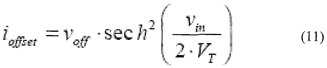
A method for eliminating an OTA input offset voltage has been proposed in [110]. This method is suitable for fabrication and quantifies and eliminates the offset for any gain configuration. An offset rejection of 4OdB was achieved in simulation [HO]. With the recognition of sufficient offset cancellation, the data was corrected in a manner representing the elimination of the offset quantified by (11) to analyze the results with offset compensation. The corresponding results are much better. Figure 22 shows effective resistance versus line voltage for various bias current setting corrected for the offset. The asymptotic behavior is
eliminated and the resistance exhibits a variance of approximately 1% with a line voltage magnitude of 2.5 volts or less.
Hardware The OTA based transmission line model was constructed in hardware using the
LM13700 dual OTA and tested. Tests similai to the PSpice simulations were conducted. The effective resistance of the circuit was calculated from measurements while varying the bias voltage. The hardware exhibits similar controllable resistance as the software simulations with only slight deviation from simulation results as shown in Figure 23. Analysis shows the offset voltage present in hardware is slightly higher, and subsequently closer to the data sheet specifications, than the PSpice model.
Multiple hardware tests were conducted to analyze the saturation effects of the circuit. The circuit was configured with a constant bias current and subjected to a varying line voltage. Figure 24 shows results of these tests for eight different resistance configurations. The slope of plots is indicative of the effective resistance and is constant for a limited line voltage range before saturation sets in similar to the simulation results. Approximately the same variance of ± 2% for line currents at 40% or less of bias current was exhibited in hardware. Figure 25 shows line current and the linear characteristic of this line current plotted against line voltage. The response is very linear and deviates only slightly in this range. This linearity is exhibited in the effective resistance of the circuit.
The effective resistance is plotted against line voltage in Figure 26. With the line voltage range between ± 2.5 volts, the variance of the effective resistance was less than 1%. This is an accurate range for operation of this model. The line model becomes less accurate, saturation effects become more severe, as the line current magnitude approaches the bias current magnitude. The linear range for this model, defined by < 1% variance, is quantified by the following relationship:

Within device limitations, the line voltage can be any magnitude as long as the relationship in (12) is maintained. This is advantageous as the linear operating voltage range has been significantly increased from a basic open loop OTA with the use of feedback. This will allow easy measurement of the bus voltages in an emulation network.
The results from both simulation and hardware were very similar and verity the operation, control and linear operating conditions of the proposed OTA based transmission line model. A three-bus prototype was constructed and tested based on these results.
Three-Bus Prototype
A network module prototype of a three-bus power system was built based on the proposed transmission line model. This design was incorporated on a single circuit board containing the transmission line components of the four networks as shown in Figure 10. It is suitable for both lossy and lossless models shown in Figures 11 and 12, respectively. The main purpose of this prototype was to validate the transmission line model application in the previously proposed DC emulation power flow technique [102], The configuration of the power system is shown in Figure 27.
The power system consists of one load, two generators and three transmission lines (A, B, C). Four independent networks containing three OTA based variable resistors were used in this emulation. The combination of these networks constitutes the complete transmission line model. The circuit board contains only the line models with terminals to attach generator and load models. The complete circuit board is shown in Figure 28. The lines (A, B, C) are highlighted in the picture to show the relationship to the power system along with the labeling of the four networks in relation to Figure 10. The input terminals for generators, loads, and power supply are also shown. For simplistic operation with fewer power supplies, all the bias currents are driven by the +15 volt supply. Configuration of the lines was accomplished by the respective values of Rabc- In addition, there are jumpers on the board that connect the transmission lines to the buses. Lines can be removed for contingency analysis or the network can be reconfigured with these jumpers. In addition, this design is scalable and subsequently larger power systems can be emulated with interconnection of multiple boards.
The network module was configured for power flow emulation. DC voltage sources were used as generators (values were obtained from a computed steady-state power flow solution) and the load was an OTA based constant current source. This is shown in Figure 29. While this setup requires the prior knowledge of the generator bus voltages, the appropriate voltage on the load bus corresponding to the correct load currents is sufficient to verify the functionality of the network module. The results were compared to results from the Power World® software package [111].
The network module was configured per the lossless system in Power World® shown in Figure 30. Table 9 shows the results, load bus voltage in per unit, from both the hardware (offset corrected) and the software computation.
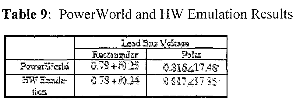
The results in this case are very accurate. From multiple runs and different load configurations the voltage magnitude error between PowerWorld® and HW was approximately 1.5% and the phase angle error was about 5%. The errors aie caused mostly by deviations from OTA to OTA and resistor tolerances.
The transmission line model presented is sufficient for lossy and lossless line models for use in the DC emulation static power flow technique mentioned. The overall model consists of multiple OTA based variable resistor circuits. The shortcomings of the hardware prototype, such as linear range, accuracy and device offsets, are mostly due to the current OTA technology. This can be overcome with further development of better performing
OTAs, which have been shown in prior research, in a similar manner in which traditional op- amps have been developed. This problem can also be tackled through a custom VLSI design.
An accurate, low-cost and remotely reconfϊgurable OTA based analog transmission line model has been developed. Simulation and hardware results verified the design, clearly defined linear operating ranges and examined the deficiencies of current off-the-shelf OTAs while pointing out methods of compensation. A three-bus power system was constructed based on the proposed model and the resultant power flow results compared favorably to those from commercially available software. This expands on the work presented in [101- 103] by the introduction of a hardware based line model with fast, remote reconfigurability suitable for the presented power flow emulation scheme.
In another preferred embodiment, simulation and/or emulation are used when dealing with large-scale power systems. They make it possible to do essential assessment in power system dispatch, operation, security and stability. Different simulation/emulation tools today are built for different applications like transient stability analysis, fault analysis, power flow studies, operational planning, etc.
ABMs are used to make flexible descriptions of electronic components or complex building block in teims of transfer function or lookup tables. In order words, a mathematical relationship is used to model a circuit segment so one will not need to design the segment component by component. Figure 31 shows a sine shaper which is a device that outputs sine value of its input signal. The left side of Figure 31 is a modified Barry Gilbert sine shaper [203] built component by component using analog devices, and the right side of Figure 31 is an ABM sine shaper [201]. The only similarity between the two is that they both take the same input signal and produce the same output.
One aspect of the invention employs transient stability analysis with the advantages of shorter computation time than current digital simulations and smaller size and cost than discrete analog emulators. One of the main disadvantages of this method is the limited accuracy due to the implementation of the analog VLSI chip.
Methodology of Core Computations Using ABMs Analog Behavioral Models (ABMs) of PSpice are used to substitute and implement mathematical equations and/or scaled relationship analog circuit representations, which describes the states of power system and emulate its behaviors. This gives a clearer picture of the end goal, design layouts and intricacies of circuit connections.
Power system core computation methodology implemented in the design of analog emulation goes through three major steps. These steps are illustrated in Figure 32. The assumptions made and detailed processes are discussed in [21 1] and [202], respectively.
Step 1: Calculating complex voltage out of generator
The generator block solves the swing equation (dynamic) with resulting power angle, δ. The power angle combines with desired voltage magnitude to give a complex voltage out of a generator.
Step II: Calculating currents in the network
The nodal and generator induced voltages interact with transmission line impedance and load (if not lumped with line impedance) to produce complex current flowing in any branch. Using admittance for simplicity and expressing in rectangular form, current is computed as in Figure 32. As depicted in Figure 33, it will require four separate networks in order to emulate complex current flowing on any branch. The approach of DC-resistive network as proposed by Fried et al. [211] is used. Transformation of the transmission line
complex impedance to its resistive value for real and imaginary part is through its complex conjugate as shown in equation 13:
X X R + .

Combining equation 13 with Figure 33, implementation of complex current computation as described in Figure 34 is shown. This means that the real part of complex current flowing in any branch is given by the sum of component currents in networks 1 and 2, and the imaginary part as the difference between component currents in networks 4 and 3, as described in equation 14.

Step III: Computation of generator real power and swing equation update
The real power out of each generator in the system is calculated as the real part of the product of generator terminal voltage and complex conjugate of the generator current:

The swing equation describes the dynamics of a generator. Its input is a mechanical power from a prime mover and which is assumed constant. The output of a generator is an electrical power, which changes in accordance with the state of the network. The swing
equation is a second order differential equation and its solution is the power angle of the generator. The power angle combines with generator internal voltage to constantly update the generator terminal voltage and hence the generator current. Figure 35 describes the continuous cycle of power system core computation. Figure 36 describes the DC-network equivalent of a real power system bus and conditions for its implementation. Analyzing a sample power system and considering an arbitrary bus k with its complex voltage values, there are 4 networks with 4 buses K1, Kπ, Km,and KIV as equivalents. For feasible bus voltages, the following conditions must be satisfied:

The feasible bus voltages condition is realizable with a constant PQ-load model [202].
Among other attributes of an analog emulator that contribute greatly to its versatility are the scale factors. Scale factors are constants that relate the values of the variables on the emulator to the values of the variables in the real system under study.
Case Studies and Results
Cases studied, which include 3-bus, 6-bus and 14-bus lossy and lossless power systems, were implemented using ABMs of PSpice. ABMs substitute real analog circuit implementation of the mathematical equations and scaled relationship that describe the states of the power system cases and emulate their behaviors. Power flow tests ere conducted on each of the cases. Similar cases were tested on industrial grade numerical simulation software, PowerWoild® v9.1 [212] and Powei System Simulation for Engineering® (PSS/E) v.28.1 [213], for benchmarking. For the validation process, the following parameters were measured and/or calculated and compared with the benchmarks. i. δj - Voltage angle difference between generator buses j and 1 (j = 2, 3,...); ii. Load bus complex voltage; iii. Complex current flowing in each branch.
Simulation results obtained from the analog emulation engines implemented on ABMs of PSpice and that of the benchmarks are presented in Tables 10 through 13. The results
compare favorably. This confirms the validity of the methodology as well as the technique of implementation .


Simulation outputs of analog emulator were measured in rectangular form and/or radians. Conversions to polar representation and/or degree were made for easy comparisons with the benchmarks. Also, for convenience and efficient analog emulation implementation, certain power system variables and parameters were represented by other circuit variables Figure 37 summarizes variable representations used in this example. Since conversion ratio used between current-voltage or power-current is 1 :1, obtained values remain representative in quantity.
Generator Model
The proposed circuit is based largely upon the classical generator model. This section presents a short review of the basics behind the generator model developed and scaling of the model to an appropriate analog circuit. The classical generator model that will be used for this example consists of a voltage source behind an impedance, where Yz 0 represents the
generator terminal voltage, Ez δ denotes the internal generator voltage and angle, and Z representing the transient reactance of the generator 'dX. The generator consisting of these elements can be seen in Figure 39.
With this model, the electrical angle, δ, is unknown, and therefore, needs to be computed. In order to determine the electrical angle, the dynamics of the generator were captured. The simplified mechanical equation that governs the motion of the generator rotor, describes the swing between the mechanical and electrical angle, otherwise known as the swing equation,
 where M is the generator inertia coefficient, D is the damping coefficient, Pe is the electrical power output, and Pm is the mechanical input power. The solution we seek, the load flow, corresponds to the steady state solution of this equation.
In order to simplify the calculation required in the analog circuit, the electrical power output of the generator will be solved in rectangular form. For converting the polar notation to rectangular form, only the real and imaginary components will be necessary and the calculation for the electrical output power of the generator model can be rewritten as the following equation:

The representation of the electrical output power will need to be applied directly into the swing equation for the calculation of the electrical angle. The functionality of the swing equation as seen in the block diagram in Figure 40, will provide us with a layout for the generator model that will be presented in the following section.
With many different models representing the generator available, we will use the classical model while neglecting damping. This will simplify the non-linear dynamics of the classical generator without significantly reducing the precision of the model [305]. With these assumptions, the swing equation (17) will reduce to only the difference between the mechanical input power and the electrical output power. After factoring in the generator inertia coefficient and taking two integration steps of the angular acceleration, the solution of the electrical power angle can be calculated in the following form:

Scaling Parameters
In order to realize a power system using analog emulation, two different scaling factors need to transpire. The time scaling parametei is for the computation speedup of the emulator while the scaling of parameter space is for the electrical angle to be represented as voltage in the circuit. Next is the introduction of the time scale factor, τ, a constant which will represent a computational speedup of τ times faster than the real-time system. This factor is directly proportional to the real time of the power system, t, for a given simulation time of the analog emulator, T. With this advantage, we can include the time scale factor in the solution of the electrical angle (19), capable of scaling the computation time of emulator in the following manner:

The time scale factor needs to be squared because of the second order nature involved in the dynamics of the classical generator model. A collaborating factor that may influence the choice of the time scale is that the error in the integration may be accentuated by long emulation times. Another scaling procedure is actual parameter scaling of the electrical angle to voltage.
Introducing the desired voltage, υ to be represented as a voltage level in the circuit that is equivalent to π radians, (20) can be rewritten as the following equation:

With the generator model and scaling parameters defined, we can proceed to develop this model using CMOS analog devices. Before selecting the devices we need to identify the circuit parameters needed to scale the power system to an analog circuit and the parameters needed to achieve reconfigur ability within the model.
Reconfigurable Generator Model
The next step of modeling addresses the concept of reconfigurability in the generator model, The actual analog circuit representing the generator needs to incorporate a programmable analog device into model to obtain controllable behaviors of the power system. Instead of the typical operational amplifiers to realize some of the components needed, the operational transconductance amplifier (OTA) will be used because of its ability to control its gain by an external current (or voltage).
The OTA has the basic properties of a voltage-controlled current source (VCCS) and the output current is obtained by:
 a product of the transconductance parameter and the differential input voltage. The transconductance, gm, can be increased or decreased as a function of the input voltage by varying the amplifier bias current, labc, according to this equation:
 as a gain and is dependent on a non-linear device constant, p and the amplifier bias current as seen in (23) [306]. Ideally, the desirable gain of an OTA would always be constant, with a linear input and output relationship. Since this is not the case, measures will need to be considered because of the errors that will result from the non-linear transconductance of the OTA.
Circuit Parameter Transformation
To achieve the difference between the mechanical input power and the electrical output power on a circuit, power is quantified as current. This introduces a circuit scaling
parameter, Kp, a constant ratio between the circuit current and model power quantity as seen below,

The analog circuit developed to solve the swing equation of the generator will consist of two first -order integrators built using OTAs [306]. The output of the double integration process is voltage representing the electrical angle and is calculated in the following manner analogous to (21).

In this equation, the Ie(V) represents electrical power which is dependent on the electrical angle. The components Ci and C2 are the values of the integration capacitor needed in the first and second integrators, respectively. The transconductance parameters, gml and gm2, are the gains of the first and second OTAs in the double integration process. These values can be reconfigured using the amplifier bias currents to correspond to various generator characteristics and a given range of speedup times.
Analog Generator Model
In order to provide the analog implementation of the algorithm described in the previous section, an approach to simulate the block diagram of the swing equation (19) needs to be realized. A functional block diagram of the generator behavioral model is made up of voltage-controlled current sources (VCCS), current-controlled voltage source (CCVS), amplifiers, integrators, and various other components that determine the electrical output power of the generator. Figure 41 represents the block diagram of the analog behavioral model of the generator.
Similar to Ie, the current, Im, is used to quantify mechanical power. The difference between this current and Ie is used as the input into the double integrator scaled as voltage. The voltage output of the double integrator is equivalent to the electrical angle given by (21). By definition, electrical power output is dependent on generator terminal voltage and current. Upon calculation of the electrical power, Pe(δ), it will be scaled to a corresponding cuπent value, Ie(V), and the process updates itself until a possible stable steady-state solution is attained.
To achieve this operation on a circuit, appropriate CMOS devices must be selected. Consideiations used for selection include minimal device power consumption, suitable device operating ranges, and transconductance. The devices selected for this model will use commercial off-the-shelf (COTS) CMOS components including the National Semiconductor LMl 3700 OTA [307] and the Analog Devices AD639 Trigonometric Converter [308].
Having the devices selected, an example of the analog emulator will be discussed, along with emulation results.
Power System Example The model in Figure 41 was used in a simple power system problem [39]. For this example, the generator delivered power to an infinite bus through a transmission line and the solution of the electrical angle can be seen as described in equation (19).
The calculation of the steady-state solution of the electrical angle of the generator can be found by solving the instantaneous generator power for the system,

The analog circuit for the single-machine power system consisted of four OTAs, a trigonometric converter, and resistors and capacitors as seen in Figure 42. The controllable gains were calculated in order to fit the circuit to the power system, which was dependent on the selection of the resistor and capacitors in the circuit. The selection of the resistor values were needed to scale the parameters to proper voltage levels for the OTAs to function within their linear operating range. The capacitor selection determined the integration time of the circuit.
The gain representing the maximum electrical power output, Pe,maχ, is transformed into the maximum current gain parameter A, which is equivalent to Ie,max- The maximum allowable current parameter will be controlled through the gain of an OTA, gmA. This can be changed for different power system parameters in the following manner from equations (24) and (26).

The two gains of the OTAs within the double integrator are considered identical to one another. Using equations (21), (24), and (25), the gains can be characterized in terms of the following:
M L

For equation (27), the power system parameters are directly associated with a controllable gain parameter. In equation (28), the controllable gain is directly associated with the generator inertia constant and the scaling parameters defined in equations (20) and (21). This allows for a completely reconfϊgurable classical generator model that provides computational speedup for conventional digital methods.
The reconfigurable classical generator model has been tested in a single-machine power system. The results of the simulation shown are from the circuit emulator of Figure 42 using PSpice and will be compared to simulation results obtained using PSpice Analog Behavior Models (ABM). This comparison is validated from previous work [310] conducted using Analog Behavior Models of sample power systems, where the results obtained compared rather favorably with traditional load flow solvers such as PSS/E and PowerWorld®.
The power system parameters and the associated circuit parameters based on the previous equations for the simulation example are listed in Table 14. For this example, the mechanical input power is fixed constant at 0.5 per unit (p.u.) while the emulator solves for a steady-state solution.
The results from the power system can be seen in Figure 43a and the results of the analog emulator can be seen in Figure 43b. With both converging to approximately the same steady-state solution, the analog emulator solved from the electrical angle of the swing equation much faster than the actual power system. This clearly demonstrates the capability of the computational speedup the analog emulator possesses with respect to real-time.

Upon closer inspection, the results of the actual angular solution are different with a large degree of error. The ABM power system model solved for the angular solution of 22.89°, while the OTA analog emulator model solved for the angular solution of 27.79°. The difference between the two results has an error of approximately 21-22%. Since the steady- state calculation of the actual electrical angle using equation (26) results in an angle of 22.89°, the analog emulator seems to produce the error. Since the present invention focuses on the study of load flow analysis of power systems, and not the intricate design of electronic devices, the offset correction method that will be applied to this example will be the post-processing of the data to correct for the offset of the devices.
To correct for the offset, the circuit was set with zero mechanical input power, Pm = 0. The circuit emulator provided an offset solution because the gains amplify the offsets within the devices. This angular offset solution was subtracted from the PSp ice emulator simulation for the given mechanical power. Figure 44 shows the results of the offset correction compared to the original results of the analog emulator with PSpice. With the offset eliminated from the PSpice solution, the corrected angular solution is now 22.74°, which is much closer to the desired solution. The results from this example and the errors calculated are tabulated in Table 15.

This single-machine infinite-bus power system example shows that the analog emulator achieves computational speedups over the real power system. The disadvantage of the analog circuit is that the accuracy of the circuit may not be as good as current digital computer methods for solving load flow. The results show with offset correction methods, an advantageous tradeoff is made between accuracy and computational speedup.
The example provided results of the advantages of the analog emulator including the ability to reconfigure system parameters and the computational speedups achieved in the circuit. The present invention is applicable to many different areas. One method would be the introduction of initial conditions on the integrator to start at a value that may be closer to a desired stable solution. Also, more complicated models could be developed to expand this model to include damping and higher order generator models. As has been demonstrated above, the present invention is useful for modeling of power systems and power system components. This can be used for fail-safe planning, as well as for operations planning. Thus, the present system is flexible enough to allow long- term planning over the life of the system, as well as to facilitate short-term operations planning for operating the system as little as 24 hours to 7 days ahead of time. This is possible since the present invention uses the hardware up to about 10 times more efficiently than all-purpose computing platforms.
The hardware of the present invention, including the FPGA and related components, are flexible enough to be customized for a variety of different calculations. Thus, although the present invention has been exemplified for power system planning, it is generally applicable to other systems requiring complex computations as well.
It is to be understood, however, that even though numerous characteristics and advantages of the present invention have been set forth in the foregoing description, together with details of the structure and function of the invention, the disclosure is illustrative only,
and changes may be made in detail, especially in matters of shape, size and arrangement of parts within the principles of the invention to the full extent indicated by the broad general meaning of the terms.
REFERENCES
[1] Feng Tu and A. J. Flueck, A message-passing distiibuted-memory parallel power flow algorithm, Power Engineering Society Winter Meeting, 2002. IEEE, Volume 1 (2002), pp 211 - 216.
[2] X. Wang and S.G. Ziavras, Parallel Direct Solution of Linear Equations on FPGA- Based Machines, Workshop on Parallel and Distributed Real-Time Systems (17th Annual IEEE International Parallel and Distributed Processing Symposium), Nice, France, April 22- 23, 2003.
[3] Keith Underwood, FPGAs vs. CPUs: Trends in peak floating point performance, ACM/SIGDA Twelfth ACM International Symposium on Field-Programmable Gate Arrays, (Monterrey, CA), February 2004.
[4] A. R. Bergen, V. Vittal, Power Systems Analysis, 2nd Edition, Prentice Hall, 2000.
[5] P. Amestoy, T. A. Davis, and I. S. Duff, An approximate minimum degree ordering algorithm, SIAM J. Matrix Anal. Applic, 17 (1996), pp. 886-905.
[6] M. Yannakakis. Computing the minimum fill-in is NP-Complete, SIAM J. AIg.
Disc. Meth., 2 (1981), pp. 77-79.
[7] W. H. Press, S. A. Teukolsky, W. T. Vettering and Brian P. Flannery, Numerical Recipes in C: the Ait of Scientific Computing, 2nd Edition, New York: Cambridge University Press, 1992.
[8] T. A. Davis and I. S. Duff, An unsymmetric-pattern multifrontal method for sparse Iu factorization, SIAM J. Matrix Anal. Applic, 18 (1997), pp. 140-158.
[101] R. Fried, R. S. Cherkaoui, and C. C. Enz, "Low-Power CMOS, Analog
Transient-Stability-Simulator for a Two-Machine Power System," presented at ISCAS, Hong-Kong, 1997.
[102] R. Fried, R. S. Cherkaoui, C. C. Enz, A. Ger-mond, and E. A. Vittoz, "Approaches for analog VLSI simulation of the transient stability of large power networks," Ieee Transactions on Circuits and Systems I-Fundamental Theory and Applications, vol. 46, pp. 1249-1263, 1999.
[103] R. Fried, R. S. Cheikaoui, C. C. Enz, A. Germond, and E. A. Vittoz, "Analog VLSI Solution to the Stability Study of Power Networks," presented at ICECS, 1996.
[104] S. P. Carullo, M. Olaleye, and C. O. Nwankpa, "VLSI Based Analog Power System Emulator for Fast Contingency Analysis," presented at Hawaii International Conference on System Science, Hawaii, 2004.
[105] J. Ramirez-Angulo and I. Grau, "Wide gm Adjustment Range, Highly Linear OTA with Linear Programmable Current Mirrors," presented at ISCAS, 1992.
[106] Z. Wang, "Making CMOS OTA a Linear Transconductor," Electronics Letters, vol. 26, pp. 1448-1449, 1990.
[107] C. A. Karybakas, C. Kosmatopoulos, and T. Laopoulos, "Improved Temperature Compensation of Otas," Electronics Letters, vol. 28, pp. 763-764, 1992.
[108] N. Semiconductor, "LMl 3700 Dual Operational Transconductance Amplifiers with Linearizing Diodes and Buffers," 2000.
[109] A. Gratz, "Operational Transconductance Amplifiers," Unpublished.
[110] R. Wunderlich, J. Oehm, A. Dollberg, and K. Schumacher, "A Linear Operational Transconductance Amplifier with Automatic Offset Cancellation and Transconductance Calibration," presented at International Conference on Electronics, Circuits and Systems, 1999.
[I l l] "PowerWorld Simulator 10.0," PowerWorld Corporation, 2004.
[201] Capture CIS version 9.2.3, Cadence Design Systems,Inc.
[202] M.B. Olaleye and CO. Nwankpa, "Analog Behavioral Models for the Purpose of Analog Emulation of Large Scale Power Systems," The Proceedings of the 36th North American Power Symposium (NAPS), pp. 97-104, August 2004.
[203] B. Gilbert, "A monolithic Microsystem for Analog Synthesis of Trigonometric Functions and Their Inverses", IEEE Journal of Solid State Circuits, Vol. SC-17, No. 6, pp. 1179-1191, December 1982.
[204] P.C. Krause, T.A. Lipo and D.P. Carroll, "Applications of Analog and Hybrid
Computation in Electric Power System Analysis," Proceedings of the IEEE, Vol. 62, No. 7, July 1974.
[205] P.G. McLaren, P. Forsyth, A. Perks and P.R. Bishop, "New Simulation Tools for Power Systems", Transmission and Distribution Conference and Exposition, 2001. IEEE/PES, vol. 1, 28, pp. 91 -96, Oct-2 Nov, 2001.
[206] A. Greenwood, Electrical Transients in Power Systems. 2nd Edition, John Wiley & Sons, Inc., New York, 1991
[207] G.A. Korn and T.M. Korn, Electronic Analogue Computers (D-C Analogue Computers), McGraw-Hill, New York, 2nd edition, 1956.
[208] M. Hirakami and W. Neugebauer, "Transient Network Analyzer Operation with Digital Computer Control and Analysis," IEEE Transactions on Power Apparatus and Systems, Vol. PAS-100, No. 4, April 1981.
[209] M. Crow, Computational Methods for Electric Power Systems. CRC Press, 2003.
[210] R. W. Newcomb and J.D. Lohn, "Analog VLSI for Neural Networks" in Handbook of Brain Theory and Neural Networks, M. Arbib Ed., Bradford Books, MIT Press, 1995 ,
[211] R. Fried, R.S. Cherkaoui, CC. Enz, A. Germond, and E.A. Vittoz, "Approaches for Analog VLSI Simulation of the Transient Stability of Large Power Networks," IEEE Transactions on Circuits and Systems-I: Fundamental Theory and Applications, Vol. 46, No.10, pp. 1249-1263, October 1999.
[212] PowerWoild Simulator v.9.1, PowerWoild Corporation, Champaign IL.
[213] Power System Simulator for Engineering (PSS/E)-28.1.4, Power Technologies, Inc.
[301] J. B. Ku and S.C. Lin, Low- Voltage SOI CMOS VLSI Devices and Circuits. New York: John Wiley & Sons Inc, 2001.
[302] R. Fried, R. Cherkaoui, C. Enz, A. Germond, and E. Vittoz, "Approaches for analog VLSI simulation of the transient stability of large power networks," IEEE Transactions on Circuits and Systems I-Fundamental Theory and Applications, vol. 46, pp. 1249-1263, 1999.
[303] J. Gu, G. G. Karady, and R. Farmer, "Real-time analysis of transient stability using reconfigurable analog VLSI," IEEE Transactions on Power Systems, vol. 18, pp. 1207- 1209, 2003.
[304] J. Yakaski and C. Nwankpa, "Insight into Reconfigurable Analog Emulation of the Classical Generator Model," presented at The 36th Annual Noith American Power Symposium, University of Idaho, Moscow, Idaho, 2004.
[305] H. E. Brown, Solution of Large Networks by Matrix Methods. New York: Wiley, 1985.
[306] R. L. Geiger and E. Sanchez-Sinencio, "Active Filter Design Using Operational
Transconductance Amplifiers: A Tutorial," in IEEE Circuits and De-vices Magazine, vol. 1, 1985, pp. 20-32.
[307] National Semiconductor, LM13700 Dual Operational Transconductance Amplifiers with Linearizing Diodes and Buffers, August 2000.
[308] Analog Devices, AD639 Universal Trigonometric Function Converter, October 1994.
[309] A. Bergen and V. Vittal, Power System Analysis, 2nd ed: Prentice Hall, 2000.
[310] M. Olaleye and C. Nwankpa, "Analog Behavioral Models for the Purpose of Analog Emulation of Large Scale Power Systems," presented at The 36th Annual North American Power Symposium, University of Idaho, Moscow, Idaho, 2004.
[311] R. Wunderlich, J. Oehm, A. Dollberg, and K. Schumacher, "A Linear Operational Transconductance Amplifier with Automatic Offset Cancellation and Transconductance Calibration," presented at The 6th IEEE International Conference on Electronics, Circuits and Systems, University of Patras, Greece, 1999.
Claims
1. An apparatus for carrying out complex computations which comprises: a field programmable gate array, said field programmable gate array programmed for implementation of Gaussian elimination by decomposition of a matrix into lower and upper triangulation factors and forward and backward elimination; memory operably connected to said field programmable gate array, and a device for maintaining pivoting information operably connected to said field programmable gate array.
2. Apparatus as claimed in claim 1, wherein said device for maintaining pivoting information comprises a lookup table and memory pointers.
3. Apparatus as claimed in claim 2, wherein said field programmable gate array implements the following Gaussian elimination for each column in the matrix loop:
(a) search the column for a pivot element;
(b) pivot if necessary;
(c) normalize a pivot column;
(d) update a remaining portion of the matrix; (e) multiply to form a sub-matrix update; and
(f) update a value or create a fill-in.
4. Apparatus as claimed in claim 3, wherein said apparatus is configured to simultaneously perform memory reads and memory writes between said field programmable gate array and said memory.
5. Apparatus as claimed in claim 4, further comprising a random access memory for storing an array of the indices of non-zero elements in the matrix, said random access memory being operably connected to said field programmable gate array.
6. Apparatus as claimed in claim 6, further comprising index rejection logic to select appropriate indices from said stored array of indices.
7. Apparatus as claimed in claim 6, wherein said memory comprises a row cache of memory of sufficient size to store a largest sub-matrix update for said computation.
8. Apparatus as claimed in claim 7, wherein further comprising a table to keep track of elimination progress.
9. Apparatus as claimed in claim 1, wherein said complex computation involves solution of at least one sparse linear system.
10. Apparatus as claimed in claim 1, configured to emulate power flow in a power transmission system.
11. A method for carrying out complex computations which comprises the steps of:
(a) implementing Gaussian elimination by decomposition of a matrix into lower and upper triangulation factors and forward and backward elimination;
(b) storing and retrieving matrix values in a memory; and
(c) maintaining pivoting information.
12. A method as claimed in claim 11, wherein said step of implementing Gaussian elimination comprises the steps of:
Gaussian elimination for each column in the matrix loop:
(a) searching a column of the matrix for a pivot element;
(b) pivoting, if necessary;
(c) normalizing a pivot column; (d) updating a remaining portion of the matrix;
(e) multiplying to form a sub-matrix update; and
(f) updating a value or create a fill-in.
13. A method as claimed in claim 12, wherein said step of storing and retrieving matrix values in memory comprises simultaneously storing and retrieving matrix values.
14. A method as claimed in claim 13, further comprising the step of tracking elimination progress to track elements that have already been eliminated.
15. A method as claimed in claim 14, further comprising the step of selecting indices from said stored array to avoid selection of matrix elements that have already been eliminated.
16. A system for emulating power flow in a power transmission system, which comprises: a power supply; a variable resistor including at least one reconfigurable operational transconductance amplifier operably connected to said power supply; and a device for measuring a current or voltage output of said system.
17. A system as claimed in claim 16, comprising at least two reconfigurable operational transconductance amplifiers for modeling power transmission in at least two directions.
18. A method for emulating a power transmission system comprising the steps of:
(a) calculating a complex voltage from at least one generator using a dynamic swing equation;
(b) calculating a complex current flowing in a branch of said power transmission system; and
(c) calculating a real power of said at least one generator; and
(d) updating the dynamic swing equation based on a result of step (c).
19. A method as claimed in claim 18, further comprising the step of: (e) solving for a steady-state solution.
20. A method as claimed in claim 19, further comprising the step of:
(f) correcting for offset of said steady-state solution by calculating an offset solution for zero mechanical input power, and subtracting the offset solution from said steady- state solution.
Priority Applications (2)
| Application Number | Priority Date | Filing Date | Title |
|---|---|---|---|
| US12/373,481 US20090292520A1 (en) | 2006-07-27 | 2007-07-27 | Solver for hardware based computing |
| US14/956,461 US9996644B2 (en) | 2006-07-27 | 2015-12-02 | Solver for hardware based computing |
Applications Claiming Priority (2)
| Application Number | Priority Date | Filing Date | Title |
|---|---|---|---|
| US82054906P | 2006-07-27 | 2006-07-27 | |
| US60/820,549 | 2006-07-27 |
Related Child Applications (2)
| Application Number | Title | Priority Date | Filing Date |
|---|---|---|---|
| US12/373,481 A-371-Of-International US20090292520A1 (en) | 2006-07-27 | 2007-07-27 | Solver for hardware based computing |
| US14/956,461 Continuation US9996644B2 (en) | 2006-07-27 | 2015-12-02 | Solver for hardware based computing |
Publications (2)
| Publication Number | Publication Date |
|---|---|
| WO2008014474A2 true WO2008014474A2 (en) | 2008-01-31 |
| WO2008014474A3 WO2008014474A3 (en) | 2008-04-03 |
Family
ID=38982399
Family Applications (1)
| Application Number | Title | Priority Date | Filing Date |
|---|---|---|---|
| PCT/US2007/074630 Ceased WO2008014474A2 (en) | 2006-07-27 | 2007-07-27 | Solver for hardware based computing |
Country Status (2)
| Country | Link |
|---|---|
| US (2) | US20090292520A1 (en) |
| WO (1) | WO2008014474A2 (en) |
Cited By (5)
| Publication number | Priority date | Publication date | Assignee | Title |
|---|---|---|---|---|
| CN104317776A (en) * | 2014-09-24 | 2015-01-28 | 南昌大学 | Sparse matrix technology-based method for solving node impedance matrix of electric power system |
| CN104391825A (en) * | 2014-11-10 | 2015-03-04 | 南昌大学 | Method of quickly solving node impedance matrix of electric power system based on Gaussian elimination method |
| CN104657337A (en) * | 2014-11-27 | 2015-05-27 | 南昌大学 | Electric power system node impedance matrix Z solving method based on CU triangular decomposition |
| CN110023167A (en) * | 2016-11-28 | 2019-07-16 | 日立汽车系统株式会社 | Electronic control unit, onboard system and power control method |
| CN110503594A (en) * | 2019-08-02 | 2019-11-26 | 长沙超创电子科技有限公司 | Video tracking device, method, system and video tracking equipment |
Families Citing this family (23)
| Publication number | Priority date | Publication date | Assignee | Title |
|---|---|---|---|---|
| CN101630273B (en) * | 2009-08-06 | 2013-01-02 | 中国电力科学研究院 | Small interference stability simulation method of electric power system |
| US9099866B2 (en) * | 2009-09-01 | 2015-08-04 | Aden Seaman | Apparatus, methods and systems for parallel power flow calculation and power system simulation |
| US8418778B2 (en) | 2010-01-07 | 2013-04-16 | Black & Decker Inc. | Power screwdriver having rotary input control |
| US9722334B2 (en) | 2010-04-07 | 2017-08-01 | Black & Decker Inc. | Power tool with light unit |
| US8473533B1 (en) * | 2010-06-17 | 2013-06-25 | Berkeley Design Automation, Inc. | Method and apparatus for harmonic balance using direct solution of HB jacobian |
| US10586162B2 (en) | 2013-03-15 | 2020-03-10 | Ppg Industries Ohio, Inc. | Systems and methods for determining a coating formulation |
| US10147043B2 (en) | 2013-03-15 | 2018-12-04 | Ppg Industries Ohio, Inc. | Systems and methods for texture assessment of a coating formulation |
| CN103163786B (en) * | 2013-04-02 | 2016-03-30 | 南车株洲电力机车有限公司 | A kind of real-time emulation method and system |
| US9235395B2 (en) * | 2013-05-30 | 2016-01-12 | National Instruments Corporation | Graphical development and deployment of parallel floating-point math functionality on a system with heterogeneous hardware components |
| NZ631063A (en) * | 2013-11-08 | 2015-10-30 | Ppg Ind Ohio Inc | Texture analysis of a coated surface using cross-normalization |
| NZ631047A (en) | 2013-11-08 | 2015-10-30 | Ppg Ind Ohio Inc | Texture analysis of a coated surface using kepler’s planetary motion laws |
| NZ631068A (en) | 2013-11-08 | 2015-10-30 | Ppg Ind Ohio Inc | Texture analysis of a coated surface using electrostatics calculations |
| US9818205B2 (en) | 2016-02-19 | 2017-11-14 | Ppg Industries Ohio, Inc. | Simplified texture comparison engine |
| US10613727B2 (en) | 2016-02-19 | 2020-04-07 | Ppg Industries Ohio, Inc. | Color and texture match ratings for optimal match selection |
| CN105703359B (en) * | 2016-03-08 | 2021-01-01 | 南昌大学 | Application of a Symmetric Sparse Factor Table Method in Calculation of Power Flow with Cartesian Coordinate PQ Decomposition Method |
| US11037330B2 (en) * | 2017-04-08 | 2021-06-15 | Intel Corporation | Low rank matrix compression |
| US11347478B2 (en) | 2018-02-23 | 2022-05-31 | Octavo Systems Llc | Analog arithmetic unit |
| US10970879B2 (en) | 2018-04-26 | 2021-04-06 | Ppg Industries Ohio, Inc. | Formulation systems and methods employing target coating data results |
| US11874220B2 (en) | 2018-04-26 | 2024-01-16 | Ppg Industries Ohio, Inc. | Formulation systems and methods employing target coating data results |
| US10871888B2 (en) | 2018-04-26 | 2020-12-22 | Ppg Industries Ohio, Inc. | Systems, methods, and interfaces for rapid coating generation |
| US11119035B2 (en) | 2018-04-26 | 2021-09-14 | Ppg Industries Ohio, Inc. | Systems and methods for rapid coating composition determinations |
| US12481867B2 (en) * | 2021-04-28 | 2025-11-25 | Arm Limited | Memory for artificial neural network accelerator |
| CN113359513B (en) * | 2021-06-30 | 2022-08-02 | 东南大学 | A hardware-accelerated parallel multi-rate electromagnetic transient real-time simulation method for converters |
Family Cites Families (8)
| Publication number | Priority date | Publication date | Assignee | Title |
|---|---|---|---|---|
| US3621209A (en) * | 1969-12-15 | 1971-11-16 | Bell Telephone Labor Inc | Machine-implemented process for insuring the numerical stability of gaussian elimination |
| US4787057A (en) * | 1986-06-04 | 1988-11-22 | General Electric Company | Finite element analysis method using multiprocessor for matrix manipulations with special handling of diagonal elements |
| JP3310632B2 (en) * | 1999-06-24 | 2002-08-05 | 建生 河村 | Optimal Power Flow Calculation System by Nonlinear Programming |
| US6601080B1 (en) * | 2000-02-23 | 2003-07-29 | Sun Microsystems, Inc. | Hybrid representation scheme for factor L in sparse direct matrix factorization |
| GB0328584D0 (en) * | 2003-12-10 | 2004-01-14 | Koninkl Philips Electronics Nv | Video data signal correction |
| JP2006085619A (en) * | 2004-09-17 | 2006-03-30 | Fujitsu Ltd | Program for solving simultaneous linear equations with band coefficient matrix |
| US7433430B2 (en) * | 2005-02-09 | 2008-10-07 | Harris Corporation | Wireless communications device providing enhanced block equalization and related methods |
| US20070136044A1 (en) * | 2005-12-13 | 2007-06-14 | Beattie Michael W | Efficient simulation of dominantly linear circuits |
-
2007
- 2007-07-27 US US12/373,481 patent/US20090292520A1/en not_active Abandoned
- 2007-07-27 WO PCT/US2007/074630 patent/WO2008014474A2/en not_active Ceased
-
2015
- 2015-12-02 US US14/956,461 patent/US9996644B2/en not_active Expired - Fee Related
Cited By (5)
| Publication number | Priority date | Publication date | Assignee | Title |
|---|---|---|---|---|
| CN104317776A (en) * | 2014-09-24 | 2015-01-28 | 南昌大学 | Sparse matrix technology-based method for solving node impedance matrix of electric power system |
| CN104391825A (en) * | 2014-11-10 | 2015-03-04 | 南昌大学 | Method of quickly solving node impedance matrix of electric power system based on Gaussian elimination method |
| CN104657337A (en) * | 2014-11-27 | 2015-05-27 | 南昌大学 | Electric power system node impedance matrix Z solving method based on CU triangular decomposition |
| CN110023167A (en) * | 2016-11-28 | 2019-07-16 | 日立汽车系统株式会社 | Electronic control unit, onboard system and power control method |
| CN110503594A (en) * | 2019-08-02 | 2019-11-26 | 长沙超创电子科技有限公司 | Video tracking device, method, system and video tracking equipment |
Also Published As
| Publication number | Publication date |
|---|---|
| US20160085893A1 (en) | 2016-03-24 |
| WO2008014474A3 (en) | 2008-04-03 |
| US9996644B2 (en) | 2018-06-12 |
| US20090292520A1 (en) | 2009-11-26 |
Similar Documents
| Publication | Publication Date | Title |
|---|---|---|
| US9996644B2 (en) | Solver for hardware based computing | |
| Chakraborty et al. | Geniex: A generalized approach to emulating non-ideality in memristive xbars using neural networks | |
| Feng et al. | Multigrid on GPU: Tackling power grid analysis on parallel SIMT platforms | |
| Li et al. | FDMAX: An elastic accelerator architecture for solving partial differential equations | |
| US7962317B1 (en) | Analytic linearization for system design | |
| Galicia et al. | Neurovp: A system-level virtual platform for integration of neuromorphic accelerators | |
| US11455144B1 (en) | Softmax calculation and architecture using a modified coordinate rotation digital computer (CORDIC) approach | |
| Johnson et al. | Performance analysis of loadflow computation using FPGA | |
| Bu et al. | Semi-implicit Krylov deferred correction methods for differential algebraic equations | |
| CN111241733A (en) | A method of optimizing finite element algorithm based on FPGA | |
| US12265779B2 (en) | Clock aware simulation vector processor | |
| Rojek et al. | Modeling power consumption of 3D MPDATA and the CG method on ARM and Intel multicore architectures | |
| Deese et al. | Utilization of field programmable analog arrays (FPAA) to emulate power system dynamics | |
| Reyneri | A Simulink-based hybrid codesign tool for rapid prototyping of FPGA's in signal processing systems | |
| Mannocci et al. | A fully integrated analogue closed-loop in-memory computing accelerator based on static random-access memory | |
| Tamuli et al. | Implementation of Jacobi iterative solver in verilog HDL | |
| Ye et al. | Fast variational interconnect delay and slew computation using quadratic models | |
| Kao et al. | A Behavior-Level Simulation Framework for RRAM-Based Deep Learning Accelerators with Flexible Architecture Configurations | |
| Soh et al. | A scalable, FPGA-based implementation of the unscented Kalman filter | |
| Baron et al. | Fast and accurate time-domain simulations with commodity graphics hardware | |
| Yan et al. | Modeling and simulation for on-chip power grid networks by locally dominant krylov subspace method | |
| Alimohammad et al. | An iterative hardware Gaussian noise generator | |
| Gu et al. | High performance molecular dynamics simulations with FPGA coprocessors | |
| Ziad et al. | On kernel acceleration of electromagnetic solvers via hardware emulation | |
| Que et al. | In-circuit tuning of deep learning designs |
Legal Events
| Date | Code | Title | Description |
|---|---|---|---|
| WWE | Wipo information: entry into national phase |
Ref document number: 12373481 Country of ref document: US |
|
| NENP | Non-entry into the national phase |
Ref country code: DE |
|
| NENP | Non-entry into the national phase |
Ref country code: RU |
|
| 121 | Ep: the epo has been informed by wipo that ep was designated in this application |
Ref document number: 07840566 Country of ref document: EP Kind code of ref document: A2 |
|
| 122 | Ep: pct application non-entry in european phase |
Ref document number: 07840566 Country of ref document: EP Kind code of ref document: A2 |