WO2005089220A2 - Multiple-stage filtering device and method - Google Patents
Multiple-stage filtering device and method Download PDFInfo
- Publication number
- WO2005089220A2 WO2005089220A2 PCT/US2005/008173 US2005008173W WO2005089220A2 WO 2005089220 A2 WO2005089220 A2 WO 2005089220A2 US 2005008173 W US2005008173 W US 2005008173W WO 2005089220 A2 WO2005089220 A2 WO 2005089220A2
- Authority
- WO
- WIPO (PCT)
- Prior art keywords
- filter
- stage
- output
- recited
- transmission environment
- Prior art date
Links
Classifications
-
- H—ELECTRICITY
- H03—ELECTRONIC CIRCUITRY
- H03H—IMPEDANCE NETWORKS, e.g. RESONANT CIRCUITS; RESONATORS
- H03H17/00—Networks using digital techniques
- H03H17/02—Frequency selective networks
- H03H17/0294—Variable filters; Programmable filters
-
- H—ELECTRICITY
- H03—ELECTRONIC CIRCUITRY
- H03H—IMPEDANCE NETWORKS, e.g. RESONANT CIRCUITS; RESONATORS
- H03H17/00—Networks using digital techniques
- H03H17/02—Frequency selective networks
- H03H17/0223—Computation saving measures; Accelerating measures
-
- H—ELECTRICITY
- H03—ELECTRONIC CIRCUITRY
- H03H—IMPEDANCE NETWORKS, e.g. RESONANT CIRCUITS; RESONATORS
- H03H17/00—Networks using digital techniques
- H03H17/02—Frequency selective networks
- H03H17/0248—Filters characterised by a particular frequency response or filtering method
- H03H17/0254—Matched filters
-
- H—ELECTRICITY
- H03—ELECTRONIC CIRCUITRY
- H03H—IMPEDANCE NETWORKS, e.g. RESONANT CIRCUITS; RESONATORS
- H03H17/00—Networks using digital techniques
- H03H17/02—Frequency selective networks
- H03H17/04—Recursive filters
- H03H17/0416—Recursive filters with input-sampling frequency and output-delivery frequency which differ, e.g. extrapolation; Anti-aliasing
- H03H17/0427—Recursive filters with input-sampling frequency and output-delivery frequency which differ, e.g. extrapolation; Anti-aliasing characterized by the ratio between the input-sampling and output-delivery frequencies
- H03H17/0438—Recursive filters with input-sampling frequency and output-delivery frequency which differ, e.g. extrapolation; Anti-aliasing characterized by the ratio between the input-sampling and output-delivery frequencies the ratio being integer
- H03H17/045—Recursive filters with input-sampling frequency and output-delivery frequency which differ, e.g. extrapolation; Anti-aliasing characterized by the ratio between the input-sampling and output-delivery frequencies the ratio being integer where the output-delivery frequency is lower than the input sampling frequency, i.e. decimation
-
- H—ELECTRICITY
- H03—ELECTRONIC CIRCUITRY
- H03H—IMPEDANCE NETWORKS, e.g. RESONANT CIRCUITS; RESONATORS
- H03H17/00—Networks using digital techniques
- H03H17/02—Frequency selective networks
- H03H17/04—Recursive filters
- H03H17/0416—Recursive filters with input-sampling frequency and output-delivery frequency which differ, e.g. extrapolation; Anti-aliasing
- H03H17/0427—Recursive filters with input-sampling frequency and output-delivery frequency which differ, e.g. extrapolation; Anti-aliasing characterized by the ratio between the input-sampling and output-delivery frequencies
- H03H17/0455—Recursive filters with input-sampling frequency and output-delivery frequency which differ, e.g. extrapolation; Anti-aliasing characterized by the ratio between the input-sampling and output-delivery frequencies the ratio being rational
-
- H—ELECTRICITY
- H03—ELECTRONIC CIRCUITRY
- H03H—IMPEDANCE NETWORKS, e.g. RESONANT CIRCUITS; RESONATORS
- H03H17/00—Networks using digital techniques
- H03H17/02—Frequency selective networks
- H03H17/06—Non-recursive filters
- H03H17/0621—Non-recursive filters with input-sampling frequency and output-delivery frequency which differ, e.g. extrapolation; Anti-aliasing
- H03H17/0635—Non-recursive filters with input-sampling frequency and output-delivery frequency which differ, e.g. extrapolation; Anti-aliasing characterized by the ratio between the input-sampling and output-delivery frequencies
- H03H17/065—Non-recursive filters with input-sampling frequency and output-delivery frequency which differ, e.g. extrapolation; Anti-aliasing characterized by the ratio between the input-sampling and output-delivery frequencies the ratio being integer
- H03H17/0664—Non-recursive filters with input-sampling frequency and output-delivery frequency which differ, e.g. extrapolation; Anti-aliasing characterized by the ratio between the input-sampling and output-delivery frequencies the ratio being integer where the output-delivery frequency is lower than the input sampling frequency, i.e. decimation
-
- H—ELECTRICITY
- H03—ELECTRONIC CIRCUITRY
- H03H—IMPEDANCE NETWORKS, e.g. RESONANT CIRCUITS; RESONATORS
- H03H17/00—Networks using digital techniques
- H03H17/02—Frequency selective networks
- H03H17/06—Non-recursive filters
- H03H17/0621—Non-recursive filters with input-sampling frequency and output-delivery frequency which differ, e.g. extrapolation; Anti-aliasing
- H03H17/0635—Non-recursive filters with input-sampling frequency and output-delivery frequency which differ, e.g. extrapolation; Anti-aliasing characterized by the ratio between the input-sampling and output-delivery frequencies
- H03H17/0685—Non-recursive filters with input-sampling frequency and output-delivery frequency which differ, e.g. extrapolation; Anti-aliasing characterized by the ratio between the input-sampling and output-delivery frequencies the ratio being rational
-
- H—ELECTRICITY
- H03—ELECTRONIC CIRCUITRY
- H03H—IMPEDANCE NETWORKS, e.g. RESONANT CIRCUITS; RESONATORS
- H03H17/00—Networks using digital techniques
- H03H17/02—Frequency selective networks
- H03H17/0223—Computation saving measures; Accelerating measures
- H03H2017/0247—Parallel structures using a slower clock
Definitions
- the present invention relates in general to wireless communication systems, such as ultrawide bandwidth (UWB) systems, including mobile transceivers, centralized transceivers, and related equipment. More specifically, the present invention relates to filters that are used in such devices process input signals, to operate an equalizer.
- UWB ultrawide bandwidth
- UWB ultrawide bandwidth
- IEEE Institute for Electrical and Electronic Engineers
- 802.15.3TM standard be drafted to cover high rate wireless personal area networks (WPANs), which covers UWB communications.
- WPANs wireless personal area networks
- DS-UWB direct sequence- ultrawide bandwidth
- PHY physical
- DS-UWB approach divides the available spectrum into upper and lower bands, the ' lower band being between 3.1 to 5.15 GHz and the upper band being between 5.825 and 10.6 GHz.
- pulse filtering/shaping may be used with BPSK/QPSK modulation with 50% excess bandwidth, root-raised- cosine impulse response.
- the chip rate, center frequency, and symbol rate in this DS- UWB proposal can be harmonically related. It is desirable for any UWB technology to .capable of supporting multiple application types.
- Two key applications are wireless in-room video distribution and handheld applications. However, each of these two applications has significantly different device requirements.
- the class of in-room video distribution applications is characterized by a need for high data rates with multiple users, robust performance, and low sensitivity to power requirements.
- any DS-UWB PHY layer proposal enable a UWB device using the IEEE 802.15.3a standard to provide both the high performance capabilities required by wireless in-room video distribution, as well as the low power/cost scalability required for high-rate handheld applications.
- FIG. 1 is a graph showing an exemplary DS-UWB symbol, according to one embodiment of the present invention
- FIG. 2 is a graph showing a ternary encoded symbol, according to one embodiment of the present invention
- FIG. 3 is a block diagram of an input structure using a multiple-stage filter implementation, according to one embodiment of the present invention
- FIG. 4 is a block diagram of an input structure using multiple parallel filters according to one embodiment of the present invention
- FIG. 5 is a block diagram of an input structure using a multiple-stage filter implementation, according to another embodiment of the present invention
- FIG. 6 is a block diagram of an input structure using multiple parallel filters according to another embodiment of the present invention
- FIG. 7 is a block diagram of a multiple stage filter in which one tap is used
- FIG. 8 is a block diagram of a multiple stage filter in which two taps are used
- FIG. 9 is a block diagram of a multiple stage filter in which three taps are used
- FIG. 10 is a block diagram of a multiple stage filter in which four taps are used
- FIGs. 11 and 12 are block diagrams of an input structure design according to one embodiment of the present invention
- FIG. 13 is a diagram illustrating switches for selecting various taps in a multiple stage filter according to one embodiment of the present invention.
- DS-UWB implementations provide significant advantages for UWB transmissions.
- This invention provides a variety of ways to enhance the operation of a DS UWB system.
- a disclosed DS-UWB embodiment uses a comparatively low complexity forward error correction (FEC) code that reduces the decoder complexity by 50% as compared to certain alternate designs, with little or no performance impact.
- FEC forward error correction
- the disclosed design relies on a simple modulation technique, e.g., binary phase shift keying (BPSK) that provides both comparatively lower complexity and more efficient architectures for multipath energy collection and inter- symbol interference (ISI) mitigation.
- BPSK binary phase shift keying
- these features support scalability to data rates exceeding 1000+ Mbps at the same time as they support low cost/power implementations that are less than half the complexity of other UWB PHYs currently under consideration by the IEEE 802.15.3a Task Group.
- the disclosed DS-UWB design presents a simple frequency plan that is harmonized with a proposed common signaling mode (CSM) that can serve as the basis of a single unified PHY standard for TG3a that supports both multi-band orthogonal frequency division multiplexing (MB-OFDM) and DS-UWB approaches for high-rate applications.
- CSM common signaling mode
- the disclosed DS-UWB embodiment is based on the use of high-rate coded UWB pulses to provide scalable performance.
- the disclosed embodiment is based on the use of variable length codes to provide scalable data rates exclusively using binary phase-shift-keying (BPSK) of UWB pulse sequences.
- BPSK binary phase-shift-keying
- Embodiments of the DS-UWB system support data rates of 28, 55, 110, 220, 500, 660, 1000, & 1320 Mbps, as shown in Table 1 below.
- each bit of data is represented by a bi-phase modulated symbol (also called a code word).
- Each symbol is in turn formed from one or more chips, which may themselves be modulated (e.g., using binary or ternary modulation).
- These chips may be formed from a variety of wavelet types. However, in many embodiments, the chips are each made up of one or more cycles of a carrier waveform.
- the chips are root-raised cosine (RRC) pulse with 30% excess bandwidth.
- each chip i.e., each pulse
- different chips can be used.
- a Gaussian monopulse could be used as a chip.
- Numerous other wavelets can be used as chips, however, depending upon the requirements of the UWB system.
- Each symbol i.e., each code word
- L chips which are used to represent a single data bit.
- each L-chip sequence may be modulated by the value of a data bit, i.e., the L chips in the sequence are each multiplied by either +1 (i.e., they remain unchanged), or by -1 (i.e., they are inverted) to indicate a digital "1" or "0.”
- This modulation process produces a binary-phase- shift-keyed (BPSK) signal.
- the L-chip sequences can themselves be encoded using a binary or ternary code. By way of example, a ternary system will be described. A binary system would follow the same modulation procedure as a ternary system, except that modulation values of 0 would not be allowed.
- individual chips within the L-chip sequence can be modulated according to a ternary value, i.e., one of +1, -1, or 0.
- a ternary value i.e., one of +1, -1, or 0.
- one 12-bit chip might have a sequence of 1 1 -1 0 0 1 -1 -1 -1 0 1 1, i.e., it is made up of a series of 12 chips, each multiplied by the corresponding value in the 12 value ternary sequence.
- FIG. 1 is a graph showing an exemplary DS-UWB symbol, according to one embodiment of the present invention.
- a 3-cycle chip used in an 8- chip symbol.
- each chip 120 is made up of a sequence of three cycles 110. Eight chips 120 are then put together to form a symbol 130 that is used to represent a bit of data.
- the symbol 130 is modulated by a data bit to represent the bit in a signal. If the symbol 130 remains unchanged, it represents one digital value, and if it is inverted, it represent the other digital value (e.g., an unchanged symbol 130 could represent a digital "1" while an inverted symbol 130 could represent a digital "0"). If coding is used, the basic sequence 130 is multiplied by a code to produce a coded sequence.
- FIG. 2 is a graph showing a ternary encoded symbol, according to one embodiment of the present invention. As in FIG. 1, the symbol in FIG. 2 uses a
- a ternary code of 1 -1 -1 0 1 0 1 -1 is used on the symbol 130 to generate a ternary encoded symbol 230.
- This coded symbol 230 is then modulated by a data bit to represent the bit in a signal such that the coded symbol 230 unchanged represents one digital value, and an inverted coded symbol 240 represent the other digital value.
- 3 or 9 cycles are used per chip.
- other numbers of cycles per chip or chips per sequence could be used in alternate embodiments.
- the nominal chip rate in the disclosed embodiment i.e., the rate at which chips are generated
- 1326 MHz is 1326 MHz.
- this chip rate could vary in alternate embodiments.
- This kind of a code can be referred to as a single-pulse code.
- the use of single-pulse codes provides optimal spectral flatness (i.e., 0 dB transmit back-off) and good performance when scaling to extremely high data rates.
- each transmitted pulse i.e., chip or wavelet
- F center the center frequency of the DS-UWB signal
- F cen ter 3 x F C i P for all of the support modes.
- center frequency Fcenter and chip frequency F Ch.P provides a significant advantage in that it allows relatively simple frequency synthesis, pulse generation and demodulation of the DS-UWB waveforms.
- the convolutional code is used in conjunction with a convolutional interleaver that helps to de-correlate any initial demodulator errors, thereby maximizing the benefits of the FEC coding. Table 1
- Table 1 shows supported data rates for low band operation in one embodiment of the present invention.
- the 9.2 Mbps mode represents a common signaling mode (CSM) that uses a chip rate of 1/3 times the nominal chip rate (and therefore 1/3 the signal bandwidth, i.e., 1/3 of the low rate of 28 Mbps); the modes using 9.2 Mbps, 28 Mbps, 110 Mbps, and 220 Mbps represent modes that are currently designated as mandatory for IEEE TG3a devices; the uncoded modes at 660 Mbps and 1320 Mbps allow for extremely high speed data transfer using very low complexity implementations; and the high-performance modes at 500 Mbps and 1000 Mbps may require FEC decoder operation at high speed (500 or 1000 MHz).
- CSM common signaling mode
- the low fading characteristics of the DS-UWB waveform allow the system to be operated even without coding to support applications that benefit from extremely high data rates with very low power consumption.
- the disclosed embodiments of a DS-UWB device can provide either 660 or 1320 Mbps using un-coded operation for short-range operation with very low complexity.
- this type of operation may be impractical for approaches that use narrowband modulation, since such systems must always have FEC to compensate for severe signal fades induced by the use of narrow modulated carriers.
- the reference pulse shape i.e., the chip shape or wavelet shape
- RRC root-raised cosine
- This baseline UWB pulse shape (in conjunction with the center frequencies) determines the desired signal operating bands.
- compliant devices can use any of a number of different techniques to produce modified pulses in order to control the spectrum of the DS-UWN transmit signal. These can include linear pulse combination, adaptive band rejection techniques, fixed or adaptive notch filters to control spectrum.
- pulse design using highspeed/low-precision DACs can be used to generate crafted pulses for precise spectral control of pulse waveforms. This approach to spectral control allows devices to provide flexible spectrum for co-existence without the need for any extra protocols or transmitter-receiver handshaking in order to negotiate dynamic band or tone usage.
- the disclosed DS-UWB design provides excellent support for multiple network (i.e., multiple piconet) operation.
- the design defines two frequency bands for network operation: a "low band” from 3.1 to 4.85 GHz and a "high band” from 6.2 to 9.7 GHz.
- a "low band” from 3.1 to 4.85 GHz
- a "high band” from 6.2 to 9.7 GHz.
- Device operation in the high band is similar to that in the low band (e.g., as shown in Table 1), except that the high band signals use center frequencies and chip rates that are twice those defined for the low band. This results in high band signals that have twice the bandwidth of low band signal and therefore twice the transmit power.
- DS-UWB uses spread spectrum.techniques to allow operation of multiple networks in a shared manner based on offset chipping rates and separate codes for each piconet. Through the use of these offsets and codes, DS-UWB ensures that any multiple access interference appears as uncorrelated Gaussian noise, thus minimizing any impact on performance and maximizing the ability to gracefully support multiple networks.
- F ch i p 1313, 1326, 1339, 1352 MHz.
- these chip rate frequencies are offset by 13 MHz per network, and all frequencies can be derived using low cost 26 MHz reference crystals (i.e., the sort widely used in cellular phones).
- two additional chip rates of 1300 & 1365 MHz can be used to allow a total of 6 networks in the low band (for a total of up to 12 networks using both low and high bands).
- alternate embodiments could use more or fewer frequency offsets, as desired, and can vary the amount of the frequency offset.
- a single baseline chip rate of 1326 MHz will be described below.
- any variety of frequency offsets can be used with this design.
- BPSK multipath energy capture and inter-symbol interference
- the symbol rate will be low (i.e., the symbol length will be large), but likewise, the multipath delay spreads of the channel will likely be longer. This provides a natural scaling of energy collection.
- a rake or channel-matched filter (CMF) structure in a receiving device will require more taps (i.e., a longer time span of symbol energy collection) and will operate at lower speeds (lower symbol rate).
- CMF channel-matched filter
- the high symbol rate will allow for higher speed rake or CMF operation, but these same structures would then require fewer taps to achieve effective multipath energy collection in the shorter multipath channels.
- the natural scaling of the multipath channel will allow a flexible implementation to provide efficient energy collection by trading longer filters at lower rates and shorter filters at high rates - the same transistors can serve both purposes in a well designed receiver.
- This same principle is true for equalizer structures: flexible linear or non-linear (DFE) structures can span more symbols at low symbol rates in longer channels and still provide high rate operation and good performance in shorter channels.
- DFE non-linear
- the present invention is applicable to any portion of a UWB device in which filters will be operated at different speeds in different modes.
- a rake receiver comprises such filters, as does an equalizer.
- the present invention should not be limited to any particular filter position, but can be used in any filter situation for which its features would be advantageous.
- the required filter scaling matches multipath channel scaling.
- the effective energy collection depends on the filter length relative to the multipath channel delay spread, and any extra taps in the input filter longer than the channel are wasted.
- multipath delay spread increases with range. This means that low data rate modes, which operate at long ranges, require long filters, while high rate modes, which operate at shorter ranges, require shorter filters.
- a flexible architecture can provide longer filters at lower data rates (i.e., longer ranges) and shorter filters at higher rates (i.e., shorter ranges). This can dramatically reduce the complexity of rake/CMF in the receiver design.
- equalizers i.e., the required length of equalizer depends on delay spread.
- FIG. 3 is a block diagram of an input structure using a multiple-stage filter implementation, according to one embodiment of the present invention.
- the input structure includes a multiple-stage filter 310.
- this multiple-stage filter 310 is a finite impulse response (FIR) filter, though in alternate embodiments infinite impulse response (HR) filters could be used.
- FIR finite impulse response
- HR infinite impulse response
- the multiple-stage filter 310 receives an input signal at an input rate equal to the chipping rate C, processes the input signal at a filter rate equal to the chipping rate C, and provides a decimated output signal also at an output rate also equal to the chipping rate C.
- the chipping rate Ci is on the order of 1326 MHz.
- currently affordable finite impulse response filters of an acceptable complexity generally can only operate up to about 200 Mbps.
- providing a filter that can operate at the current chipping rate C would be very expensive. It is therefore desirable to provide an alternate design that reduces the speed at which the multiple-stage filter 310 must operate. It is of course understood that speeds of components will continue to increase with time.
- FIG. 4 is a block diagram of an input structure using multiple parallel filters according to one embodiment of the present invention.
- the input structure includes first through N th multiple-stage filters 410 ⁇ -41 O N and an N-input switch 420.
- the first through N th multiple-stage filters 410I-410 N each receive the same input signal at an input rate equal to the chipping rate C.
- O ftN operat .e.s. at , a filter rate equal to — 1 the N C chipping rate (i.e., — ).
- the N-input switch 420 operates at the chipping rate C, N cycling through the outputs of each of the first through N ft multiple-stage filters
- this circuit C allows each individual filter to operate at a lower rate of — , while providing an
- FIG.4 discloses the use of an N-input switch 420, alternate embodiments could provide the outputs of the N multiple stage filters 410 ⁇ -41 ON as a parallel bus. In the disclosed DS-UWB design, however, the filters need only match symbols, and not chips, and so can operate at the symbol rate, not the chipping rate (which will be a shorter rate for all situations excepts a symbol length of 1).
- FIG. 5 is a block diagram of an input structure using a multiple-stage filter implementation, according to another embodiment of the present invention. In this C embodiment the multiple stage filter operates as the symbol rate — , rather than the
- the input structure includes a multiple-stage filter 510.
- the multiple-stage filter 510 is an FIR filter, though an
- the multiple-stage filter 510 receives an input signal at an input rate equal to the chipping rate C, processes the input signal at a filter rate corresponding to the symbol rate equal to the chipping rate C divided by the symbol C length L (i.e., at a filter rate of — ), and provides a decimated output signal also at an input rate equal to the chipping rate C.
- the chipping rate C output rate also equal to the symbol rate (i.e., at an output rate of — ).
- the chipping rate C is on the order of 1326 MHz.
- currently affordable finite impulse response filters of an acceptable complexity generally can only operate up to about 200 Mbps. This means that for symbol lengths of 7 or greater, and a chipping rate of 1326 MHz, the symbol rate will be below 200 MHz, and so a single multiple-stage filter 510 can properly process a signal. (As the chipping rate varies in alternate embodiments, the relative symbol rate that allows for a single multiple-stage filter 510 will also vary.) It is also possible, however, to provide multiple filters in parallel in place of the single multiple-stage filter 510 of FIG. 5. FIG.
- the input structure includes first through M ⁇ multiple-stage filters 610 I -610 M and an M-input switch 620.
- the first through M a multiple-stage filters 610 I -610 M each receive the same input signal at an input rate equal to the chipping rate C.
- the M-input switch 620 operates at the symbol rate — , L- M L cycling through the outputs of each of the first through M ⁇ multiple-stage filters
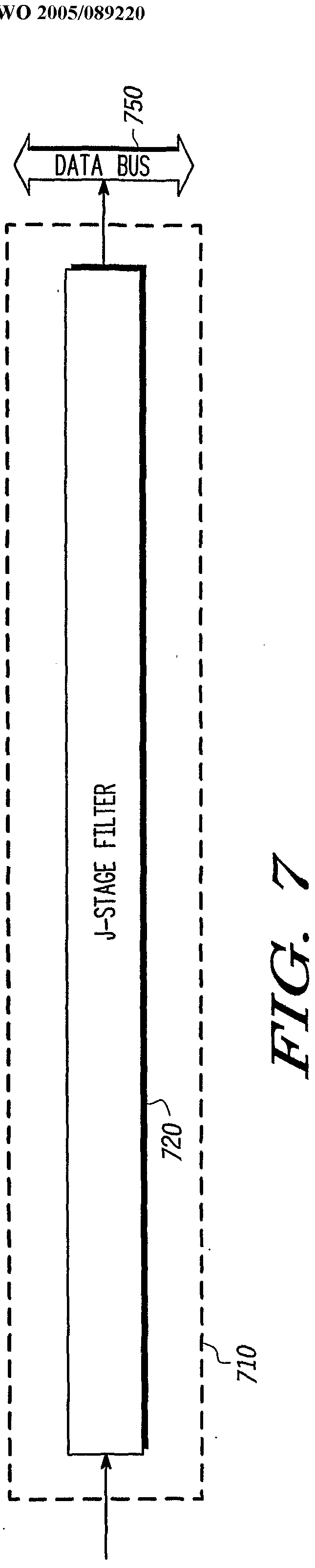
- FIGs. 7 to 10 are block diagrams showing a multiple stage filter with multiple taps according to one embodiment of the present invention.
- FIG. 7 is a block diagram of a multiple stage filter in which one tap is used
- FIG. 8 is a block diagram of a multiple stage filter in which two taps are used
- FIG. 9 is a block diagram of a multiple stage filter in which three taps are used
- FIG. 10 is a block diagram of a multiple stage filter in which four taps are used.
- a J-stage filter 710 can be tapped at the front and back to form a single J-stage filter 720. But, as shown in FIG.
- the same J-stage filter 710 can be tapped at the front, in the middle, and at the end to form a first (J/2)-stage filter 820 and a second (J/2)-stage filter 825.
- the J-stage filter 710 can be tapped at the front, one-third of the way through, two-thirds of the way through, and at the end to form a first (J/3)-stage filter 920, a second (J/3)-stage filter 925, and a third (J/3)-stage filter 930.
- FIG. 9 the same J-stage filter 710 can be tapped at the front, in the middle, and at the end to form a first (J/2)-stage filter 820 and a second (J/2)-stage filter 825.
- the J-stage filter 710 can be tapped at the front, one-third of the way through, two-thirds of the way through, and at the end to form a first (J/3)-stage filter 920, a second (J/3)-stage filter 925
- the J-stage filter 710 can be tapped at the front, one-quarter of the way through, halfway through, three-quarters of the way through, and at the end to form a first (J/4)-stage filter 1020, a second (J/4)-stage filter 1025, a third (J/4)-stage filter 1030, and a fourth (J/4)-stage filter 1035.
- the individual stages will each receive the same input signal at the chipping rate C.
- Each stage will then operate at a filter rate equal to the symbol rate divided by the number of stages (e.g., in FIG. 9, each of the first through third (J/3)-stage filters 920, 925, and 930 will operate at the symbol rate divided by 3, i.e.,
- the outputs of the various stages 720, 820, 825, 920, 925, 930, 1020, 1025, 1030, and 1035 are all provided to a data bus 950 when appropriate for further processing.
- an output switch could then be provided with each J-stage filter, of the sort shown in FIGs. 4 and 6. This switch would be able to operate at a speed that will allow it to switch between the maximum number of lower-stage filters that can be arranged and still output at the desired speed. When fewer than the largest number of stages are used, the switch could select between the stages used, and operate at an appropriately adjusted switching rate.
- the outputs of each filter could be provided as a parallel bus.
- J is chosen to be a multiple of 12. This allows ⁇ each J-stage filter to at the very least be split into 2, 3, 4, 6, or 12 equal filter portions. However, some alternate embodiments could use values of J that are multiples of 6.
- each filter can at least be split into 2, 3, or 6 equal filter portions.
- Further embodiments could use values of J that are not multiples of 12 or 6.
- J 16.
- the chipping rate is 1326 MHz, and the data rates shown in Table 1 are used.
- the code word length can vary from 1 to 24, and a variety of FEC rates can be used.
- the code word length is 1, the system operates at its highest speed, i.e., about 1320 Mbps.
- a single 24-stage filter can be tapped to
- a 12-input switch operating at 660 MHz will sequentially select the outputs of each of the two-stage filters to provide a data output signal at 660 MHz. If rate FEC is used, this output rate will drop by V ⁇ to about 500 MHz.
- Table 1 when a code word length of 2 is used, the maximum range is between 3 and 7.3 meters, depending upon whether FEC is used. Because these ranges remain short, there will still be few multipath elements to the signal, allowing for a relatively low multipath channel delay spread. As a result of this, the receiver will not need to use input filters with more than two stages to collect sufficient signal energy. When the code word length is 3, the system operates at one-third of its highest speed, i.e., about 440 Mbps. In this embodiment a single 24-stage filter can be tapped
- the system When the code word length is 6, the system operates at one-sixth of its highest speed, i.e., about 220 Mbps.
- a single 24-stage filter can be tapped to effectively provide 4 six-stage filters, which each operate at x th of the symbol rate,
- Vz FEC Vz FEC
- the output rate will drop by A to about 110 MHz.
- Table 1 when a code word length of 6 is used, the maximum range is 18.3 meters. This distance will allow some multipath elements to the signal, allowing for some multipath channel delay spread. However, the spread will be small enough that the receiver will not need to use input filters with more than six stages to collect sufficient signal energy.
- the code word length is 12, the system operates at one-twelfth of its highest speed, i.e., about 110 Mbps.
- a single 24-stage filter can be tapped to effectively provide 2 twelve-stage filters, which each operate at A of the
- the output rate will drop by l A to about 55 MHz.
- Table 1 when a code word length of 12 is used, the maximum range is 22.1 meters. This distance will allow large multipath elements to the signal, allowing for significant multipath channel delay spread. However, the spread will be small enough that the receiver will not need to use input filters with more than twelve stages to collect sufficient signal energy.
- the code word length is 24 in a DS-UWB mode, the system operates at one-twenty-fourth of its highest speed, i.e., about 55 Mbps.
- a single 24-stage filter is not tapped at any intermediate locations, but is operated as a single twenty-four-stage filter, which operates at the symbol rate, i.e., 55 MHz.
- the output of this filter is directly provided as a data output signal at 55 MHz. Since ⁇ FEC is used in this embodiment, the output rate will drop by X A to about 28 MHz.
- Table 1 when a code word length of 24 is used in DS-UWB mode, the maximum range is 29.4 meters. This distance will allow large multipath elements to the signal, allowing for significant multipath channel delay spread. The spread in the disclosed embodiment will be large enough that the receiver can use an input filters with twenty-four stages to collect sufficient signal energy.
- the system can also operate in the common signaling mode (CSM). This will lower the data rate to 9.2 Mbps, but will allow communication between DS-UWB devices and MB-OFDM devices.
- CSM common signaling mode
- a 24 input switch, a 12-input switch, an 8-input switch, a 6-input switch, a 4- input switch, a 3 -input switch, and a 2-input switch should be used
- a single 24-input switch can be used that can be set to rotate through a smaller number of it's available inputs, effectively operating as smaller input switches as needed.
- alternate embodiments could alter the operation of the fragmenting process, so long as the filter speed of each filter portion does not exceed a maximum easily achievable filter rate. For example, although the above embodiment discloses a filter rate of 55 MHz in each filter portion, the arrangement of filters could be altered such that the filter rate was 110 MHz. In this case more filters could be provided for each path than the minimum required.
- filter rates are kept constant for each stage, alternate embodiments could vary the filter rates among the stages, again so long as they always remain below a maximum easily achievable filter rate.
- each of the above exemplary embodiments is disclosed using a single 24-stage filter, alternate embodiments could use more than one multiple-stage filter in parallel, reducing the required size of each individual filter.
- the value of J can vary, different chipping rates can be used, the code word length can vary, and the FEC rates can be altered or FEC eliminated altogether. If, however, the filters are to be used for acquisition, the filter arrangement must be able to provide a number of parallel filters equal at least to the code word length L.
- FIGs. 11 and 12 are block diagrams of an input structure design according to one embodiment of the present invention.
- the input structure includes a first J-stage filter 1110, a second J-stage filter 1120, and a switch 1130.
- the input structure is operated such that the first and second J-stage filters 1110 and 1120 each perform as a single filter.
- Each J-stage filter functions at half the output rate and the switch 1130 operates at the output rate, selecting between the output of the first and second J-stage filters 1110 and 1120 in turn.
- FIG. 11 is a first J-stage filter 1110, a second J-stage filter 1120, and a switch 1130.
- the input structure is operated such that the first and second J-stage filters 1110 and 1120 each perform as a two filters.
- the first J-stage filter 1110 operates as first and second (J/2)-stage filters 1113 and 1116
- the second J-stage filter 1120 operates as third and fourth (J/2)-stage filters 1123 and 1126.
- Each (J/2)- stage filter functions at one-quarter the output rate and the switch 1130 operates at the output rate, selecting between the output of the first through fourth (J/2)-stage filters 1113, 1116, 1123, and 1126 in turn.
- the number of parallel J-stage filters can be altered, and the number of stages and taps in each of the J-stage filters can be varied.
- FIG. 13 is a diagram illustrating switches for selecting various taps in a multiple stage filter according to one embodiment of the present invention.
- the disclosed multiple-stage filter 1310 includes six separate filter stages 1331-1336.
- the filter 1310 also includes first through fifth input switches 1341-1345, first through fifth output switches 1351-1355, and first through fifth isolation switches 1361-1365.
- the input of the first filter stage 1331 and the inputs of the first through five input switches 1341-1345 are connected to an input signal that is received at the input rate (e.g., at the chipping rate Q.
- the outputs of the first through fifth filter stages 1331-1335 are connected to both the inputs of the first through fifth output switches 1351-1355, respectively, and the inputs of the first through fifth isolation switches 1361-1365, respectively.
- the outputs of the first through fifth isolation switches 1361-1365 are connected to the inputs of the second through sixth filter stages 1332- 1336, respectively.
- the output of the n-input switch 1320 is provided as an output signal ' that is provided at the output rate C (e.g., at the symbol rate — ).
- the various switches 1341-1345, 1351-1355, and 1361-1365 are manipulated to create the needed filter stages.
- Table 2 shows how the filter disclosed in FIG. 13 can be used as a 1 -stage filter, a 2-stage filter, a 3 -stage filter, and a 6-stage filter by controlling the switches 1341-1345, 1351-1355, and 1361-1365.
- an "O” indicates an open switch
- a "C” indicates a closed switch.
- the first through fifth input switches 1341-1345 are designated as switches 1A-5A
- the first through fifth output switches 1351-1355 are designated as switches 1B-5B
- the first through fifth isolation switches 1361-1365 are designated as switches 1C-5C.
- the switches in this embodiment can be any kind of digital switch, e.g., those designed from transistors.
- FIG. 13 shows a six-stage filter, this is by way of example only. Alternate embodiments can use different stages as needed. The selection process for various stages will be analogous to that shown above for a filter 1310 with six stages.
- the switches 1341-1345, 1351-1355, and 1361-1365 can be operated to create other sub-filters that are not equal in size. For example it is possible to create two filters, one 2-stage filter and one 4-stage filter, or one 1 -stage filter and one 5- stage filter. For larger numbers of stages, additional possibilities exist.
- the switches 1341-1345, 1351-1355, and 1361-1365 can be operated such that not all stages are used.
- the input signal can be provided at an over-sampled input rate of (C x s), where s is an over-sampling factor.
- C x s an over-sampling factor.
- s will vary between 1 and 4, though larger values can be used for some implementations.
- the disclosed embodiments operate as the symbol speed, the present invention is equally applicable to situations in which the filters are operating at a filter speed equal to the chipping rate.
- MB- OFDM implementation that uses a high speed FFT engine for demodulation. This approach requires the full FFT calculation and frequency-domain equalization, regardless of the delay spread of the channel.
- both the MB-OFDM waveform and the FFT-based processing are always "tuned” to collect multipath energy over a 60.5 ns interval (the length of the guard interval). If the multipath delay spread is short, the MB-OFDM FFT engine significantly "over-processes" the signal, yet the signal still suffers Rayleigh fading because multipath is not resolved. If the delay spread is very long (> 60 ns), the MB- OFDM waveform will fail to prevent ISI and performance will again suffer - unless an additional time-domain equalizer is also implemented (extra complexity). The operation of.
- the energy capture and equalization functions at the symbol rate for DS-UWB also lead to a significant advantage over other DS approaches, such as MBOK.
- CMF structures that match to a single "chip” would need to operate at the higher chip rate, not the symbol rate.
- BPSK rake or CMF receivers could operate at much lower rates than MBOK receivers depending on the symbol rate.
- the scaling of DFE structures for large MBOK constellations leads to high complexity requirements in order to realize the benefits of equalization.
- the present DS-UWB design provides several advantages in complexity and chip size.
Abstract
Description


Claims


Priority Applications (1)
| Application Number | Priority Date | Filing Date | Title |
|---|---|---|---|
| EP05728353A EP1728347A4 (en) | 2004-03-12 | 2005-03-11 | Multiple-stage filtering device and method |
Applications Claiming Priority (4)
| Application Number | Priority Date | Filing Date | Title |
|---|---|---|---|
| US55244704P | 2004-03-12 | 2004-03-12 | |
| US60/552,447 | 2004-03-12 | ||
| US10/868,948 | 2004-06-17 | ||
| US10/868,948 US7002940B2 (en) | 2004-03-12 | 2004-06-17 | Multiple-stage filtering device and method |
Publications (2)
| Publication Number | Publication Date |
|---|---|
| WO2005089220A2 true WO2005089220A2 (en) | 2005-09-29 |
| WO2005089220A3 WO2005089220A3 (en) | 2005-10-27 |
Family
ID=34922771
Family Applications (1)
| Application Number | Title | Priority Date | Filing Date |
|---|---|---|---|
| PCT/US2005/008173 WO2005089220A2 (en) | 2004-03-12 | 2005-03-11 | Multiple-stage filtering device and method |
Country Status (3)
| Country | Link |
|---|---|
| US (1) | US7002940B2 (en) |
| EP (1) | EP1728347A4 (en) |
| WO (1) | WO2005089220A2 (en) |
Families Citing this family (13)
| Publication number | Priority date | Publication date | Assignee | Title |
|---|---|---|---|---|
| US8144572B2 (en) * | 2004-09-14 | 2012-03-27 | Qualcomm Incorporated | Detection and mitigation of interference and jammers in an OFDM system |
| US7769112B2 (en) * | 2005-09-29 | 2010-08-03 | Freescale Semiconductor, Inc. | Method and system for generating wavelets |
| US8023409B2 (en) * | 2005-12-20 | 2011-09-20 | Broadcom Corporation | Method and system for reconfigurable pattern filtering engine |
| WO2007081327A1 (en) * | 2006-01-11 | 2007-07-19 | Mitsubishi Electric Research Laboratories | Method and apparatus for generating dynamically varying time hopping sequences for uwb signals |
| US7869529B2 (en) | 2006-06-14 | 2011-01-11 | Qualcomm Incorporated | System, method and computer-readable medium for detection and avoidance (DAA) of victim services in ultra-wideband systems (UWB) |
| US20080310485A1 (en) * | 2007-06-15 | 2008-12-18 | Qualcomm Incorporated | System and methods for controlling modem hardware |
| WO2009032214A2 (en) * | 2007-08-29 | 2009-03-12 | The Regents Of The University Of California | Network and device aware video scaling system, method, software, and device |
| GB2452309A (en) * | 2007-08-31 | 2009-03-04 | Agilent Technologies Inc | Circuit for sample rate conversion |
| US8081691B2 (en) | 2008-01-14 | 2011-12-20 | Qualcomm Incorporated | Detection of interferers using divergence of signal quality estimates |
| US10015290B2 (en) * | 2014-03-14 | 2018-07-03 | Samsung Electronics Co., Ltd. | Method and apparatus for encoding and decoding packet |
| KR102303749B1 (en) * | 2014-03-14 | 2021-09-23 | 삼성전자주식회사 | Method and apparatus for encoding and decoding packet |
| CN107770848B (en) * | 2016-08-15 | 2020-09-11 | 华为技术有限公司 | Method and apparatus for transmitting wake-up packet in communication system |
| US9806732B1 (en) * | 2017-03-10 | 2017-10-31 | SiTune Corporation | Calibration of high speed ananlog-to-digital converters |
Citations (1)
| Publication number | Priority date | Publication date | Assignee | Title |
|---|---|---|---|---|
| WO1999034519A1 (en) | 1997-12-31 | 1999-07-08 | Samsung Electronics Co., Ltd. | Decimation filtering apparatus and method |
Family Cites Families (8)
| Publication number | Priority date | Publication date | Assignee | Title |
|---|---|---|---|---|
| DE8706928U1 (en) * | 1987-05-14 | 1987-08-06 | Ant Nachrichtentechnik Gmbh, 7150 Backnang, De | |
| US5682125A (en) * | 1994-09-21 | 1997-10-28 | Seagate Technology, Inc. | Adaptive analog transversal equalizer |
| GB2298101B (en) * | 1995-02-20 | 1999-04-28 | Sony Uk Ltd | Frequency separation of image data |
| US7130292B2 (en) * | 2000-06-02 | 2006-10-31 | Essex Corporation | Optical processor enhanced receiver architecture (opera) |
| DE10042930B4 (en) * | 2000-08-31 | 2005-07-14 | Infineon Technologies Ag | Digital filter |
| US7061970B2 (en) * | 2000-11-14 | 2006-06-13 | Irving Reed | Self-synchronizing adaptive multistage receiver for wireless communication systems |
| US6963890B2 (en) * | 2001-05-31 | 2005-11-08 | Koninklijke Philips Electronics N.V. | Reconfigurable digital filter having multiple filtering modes |
| US8284886B2 (en) * | 2003-01-17 | 2012-10-09 | Texas Instruments Incorporated | Radio frequency built-in self test for quality monitoring of local oscillator and transmitter |
-
2004
- 2004-06-17 US US10/868,948 patent/US7002940B2/en not_active Expired - Fee Related
-
2005
- 2005-03-11 EP EP05728353A patent/EP1728347A4/en not_active Withdrawn
- 2005-03-11 WO PCT/US2005/008173 patent/WO2005089220A2/en active Application Filing
Patent Citations (1)
| Publication number | Priority date | Publication date | Assignee | Title |
|---|---|---|---|---|
| WO1999034519A1 (en) | 1997-12-31 | 1999-07-08 | Samsung Electronics Co., Ltd. | Decimation filtering apparatus and method |
Also Published As
| Publication number | Publication date |
|---|---|
| WO2005089220A3 (en) | 2005-10-27 |
| EP1728347A4 (en) | 2008-06-11 |
| EP1728347A2 (en) | 2006-12-06 |
| US7002940B2 (en) | 2006-02-21 |
| US20050201287A1 (en) | 2005-09-15 |
Similar Documents
| Publication | Publication Date | Title |
|---|---|---|
| WO2005089220A2 (en) | Multiple-stage filtering device and method | |
| EP2617137B1 (en) | A receiver for use in an ultra-wideband communication system | |
| US7221911B2 (en) | Multi-band ultra-wide band communication method and system | |
| US7675960B2 (en) | Method for generating communication signal sequences having desirable correlation properties and system for using same | |
| US7474705B2 (en) | Scalable ultra-wide band communication system | |
| US20020181388A1 (en) | Communication system using orthogonal wavelet division multiplexing (OWDM) and OWDM-spread spectrum (OWSS) signaling | |
| US20080298435A1 (en) | Common Air Interface Supporting Single Carrier and OFDM | |
| US20080225963A1 (en) | Ultra-wideband communication systems and methods | |
| US7539271B2 (en) | System and method for multi-band ultra-wide band signal generators | |
| WO2003034676A2 (en) | Change of sampling rate with single carrier and multicarrier waveforms | |
| US10348360B2 (en) | Signal representing data, method and device for generating such signal and method and device for determining the represented data from such signal | |
| WO2005069506A1 (en) | A method and transmitter, receiver and transceiver systems for ultra wideband communication | |
| Hosseini et al. | Wavelet packet based multicarrier modulation for cognitive UWB systems | |
| Saberinia et al. | Single and multi-carrier UWB communications | |
| WO2005069523A1 (en) | A system, a transceiver structure for use therein and a method of processing signals in such a system | |
| WO1999065154A1 (en) | One-bit correlator rake receiver | |
| CN100576786C (en) | Multiple-stage filtering device and method | |
| US7242707B1 (en) | Multiband ultra wideband communications | |
| Sadough et al. | Performance evaluation of IEEE 802.15. 3a physical layer proposal based on Multiband-OFDM | |
| Jain et al. | OWSS: a new signaling system for 100-150-Mb/s wireless LANs | |
| Kumar et al. | A review on decade of multi-rate filters | |
| Wu et al. | Carrier-less, single and multi-carrier UWB radio technology | |
| US20100226414A1 (en) | System and a Method for Wireless Transmission and Reception of Concatenated Impulse Radio Ultra-Wideband Data Bursts | |
| Mehra | FPGA Based Efficient WCDMA DUC for Software Radios | |
| Zhao et al. | Performance of UWB communication based on dynamic bandwidth direct sequence |
Legal Events
| Date | Code | Title | Description |
|---|---|---|---|
| AK | Designated states |
Kind code of ref document: A2 Designated state(s): AE AG AL AM AT AU AZ BA BB BG BR BW BY BZ CA CH CN CO CR CU CZ DE DK DM DZ EC EE EG ES FI GB GD GE GH GM HR HU ID IL IN IS JP KE KG KP KR KZ LC LK LR LS LT LU LV MA MD MG MK MN MW MX MZ NA NI NO NZ OM PG PH PL PT RO RU SC SD SE SG SK SL SM SY TJ TM TN TR TT TZ UA UG US UZ VC VN YU ZA ZM ZW |
|
| AL | Designated countries for regional patents |
Kind code of ref document: A2 Designated state(s): BW GH GM KE LS MW MZ NA SD SL SZ TZ UG ZM ZW AM AZ BY KG KZ MD RU TJ TM AT BE BG CH CY CZ DE DK EE ES FI FR GB GR HU IE IS IT LT LU MC NL PL PT RO SE SI SK TR BF BJ CF CG CI CM GA GN GQ GW ML MR NE SN TD TG |
|
| WWE | Wipo information: entry into national phase |
Ref document number: 200580008021.7 Country of ref document: CN |
|
| NENP | Non-entry into the national phase |
Ref country code: DE |
|
| WWW | Wipo information: withdrawn in national office |
Country of ref document: DE |
|
| WWE | Wipo information: entry into national phase |
Ref document number: 2005728353 Country of ref document: EP |
|
| 121 | Ep: the epo has been informed by wipo that ep was designated in this application | ||
| WWP | Wipo information: published in national office |
Ref document number: 2005728353 Country of ref document: EP |