METHODS TO PRODUCE ROBUST MULTILAYER CIRCUITRY FOR
ELECTRONIC PACKAGING
Field of the Invention
The present invention relates to methods for the fabrication of interconnect substrates commonly known as electronic packaging. Specifically, the invention relates to methods for the production of multilayer electronic packaging for use as an intermediate level of electrical interconnect between an integrated circuit(s) and a printed wiring board and/or as the printed wiring board itself. Background of the Invention
Electronics have become pervasive in consumer products. Even seemingly mundane devices have electronic systems with a level of sophistication that would have seemed impossible a couple of decades ago. The pressure to provide ever more sophisticated systems for these products in both smaller packages and at lower cost is relentless.
Because commodity products such as telephones now require a level of sophistication equal to or greater than what was present only in state of the art military and aerospace applications only a few years ago, manufacturers have increasingly abandoned ceramic electronic packaging technologies in favor of lower cost polymer- based electronic packaging technologies. All of the polymer-based packaging technologies heavily leverage the conventional methodology of manufacturing printed wiring boards. This reliance offers both advantages and disadvantages.
The advantages of leveraging printed wiring board manufacturing techniques are the availability of a large, well established infrastructure and economies of scale. The disadvantages primarily stem from the fact that performance and wiring density tolerances for printed wiring boards have historically been relatively lenient. Further, conventional techniques to produce printed wiring boards create a significant amount of surface topology at every layer, thus limiting the practical number of total layers that can be combined into a multilayer structure and increasing the potential for low assembly yields when components with non-compliant lead structures like the increasingly popular 'area array' configurations are used. Due to this, the materials and techniques used for the fabrication of printed wiring boards have insufficient capabilities with respect to achievable circuit density, multilayering, electrical performance, thermal performance, yield and reliability for current and future electronic products.
Of these disadvantages, the density limitation is the most acute. Density requirements are primarily driven by the proliferation of portable devices, but even 'fixtured' electronic systems are facing size reduction pressures. However, as printed wiring board technologies are pushed to meet the new density requirements, yields fall and the cost advantage is eroded.
A number of approaches have been developed, and several more are currently under development, to extend the beneficial aspects of conventional printed wiring board technology to higher density and higher performance electronic packaging; however, all of the currently available methods suffer from serious deficiencies.
Some manufacturers have addressed the inherent density limitations of etching copper circuits by developing what are known as 'additive' or 'semi-additive' methods to produce circuits. Conventional circuit fabrication techniques are subtractive in nature. One begins with a metal foil affixed to a substrate material and then selectively chemically etches away the unwanted metal by use of a protective
polymer mask. The most detrimental aspect of this method is that the chemical etching process is isotropic. Since the etchant solution attacks the sidewalls of the circuits as they are formed, the resulting circuits have an upside-down trapezoidal morphology in which the metal under the protective mask has been undercut by the etchant. Depending on the thickness of the metal and the size of the features one is attempting to resolve, the entire feature can end up overetched to such an extent that it becomes detached from the substrate or almost disappears. Because the isotropic nature of chemical etching is an inherent characteristic of the process, careful monitoring can only mitigate the problem to some extent. Likewise, use of progressively thinner metal foils to combat the undercut and achieve finer geometries has limited practical utility and a quickly diminishing return.
The so-called "additive" solution to this problem is to deposit circuits directly onto the substrate in their desired configurations by using polymer thick film materials and screen printing techniques. The problems with this approach are twofold: the conductive pathway within such polymer thick film materials is from discrete particle to discrete particle resulting in an inherently unstable conductor, and the resolution capabilities of techniques such as screen printing are limited.
The materials and methods disclosed in U.S. Patent No. 5,716,663 alleviate both of the deficiencies polymer thick film additive approaches by providing a metallurgically alloyed conduction pathway and a means by which very fine circuit geometries can be defined by photolithographic methods; however, the inherently lower bulk conductivity value of the conductive composite in comparison to copper makes this solution unsuitable for applications such as those which require a high current carrying capacity or very high signal speed.
Industry's answer to these limitations has been to develop the so-called 'semi- additive' techniques. In these techniques, a uniform, thin layer of conductive material (hereafter referred to as the seed layer) is deposited onto the substrate. This seed layer is then either etched in the pattern of the circuits, or, more commonly, it is coated with
a photolithographic resist material that is patterned to reveal selected portions of the seed layer for subsequent electroplated deposition of the actual circuits.
When the seed layer is metal, defining the circuits by etching can be successfully used to create circuitry of finer dimensions than can be produced by conventional means, but, as detailed above, use of thin metal coatings in a subtractive technique is a self-limiting process. Using the seed layer as a shorting element for subsequent electroplating through a patterned photolithographic mask is thus the preferred methodology.
The seed layer can be any one of a number of different species including: graphite, inherently conductive polymers, polymers filled with conductive particles, and, most commonly, sputtered or electroless chemical plating deposited metal. The most common seed layer is electroless plating deposited copper. All of the available materials suffer from either poor adhesion at the seed layer to substrate interface, poor adhesion at the seed layer to electroplated circuit interface, expensive or complicated processing to achieve the seed layer, inconsistencies in the subsequent electroplated circuits, or a combination thereof. Yet another deficiency of prior art seed layers is that the processes utilized to remove the undesired portions of the seed layer after the circuits have been electroplated are typically chemical in nature, and thus may be incompatible with some substrate materials which would otherwise be desirable. In addition, these chemical removal processes can introduce contaminants and defects that affect the reliability of the finished products. Further, seed layers deposited by an electroless plating method can only be applied to certain compatible surfaces which severely restricts the utility of the process by limiting it to specific polymeric dielectrics and/or substrates.
The second circuit density limitation in conventional printed wiring board manufacturing techniques is the production of vertical electrical interconnections between layers in multilayer circuits. The standard method to create such interconnects is to laminate several double sided circuits together with interleaved
polymer dielectrics, drill through the entire stack every place that an interconnection is required, and then metallize the holes to connect the layers within. This method has a myriad of density, reliability and fabrication limitations. The first limitation is that the drilled holes consume a large percentage of the total area of every layer. The second limitation is that holes that are necessary to connect only a couple of layers must be present on every layer. Further, all of these holes must be relatively large since they typically cannot be cost-effectively drilled when the drill bits become smaller than 0.008 inches in diameter. With regard to performance, the quality of the plating in the center region of the holes becomes progressively worse as the layer count increases. Additionally, the circuits must be routed over longer, circuitous pathways thus resulting in inferior electrical performance. From a reliability standpoint, the thermal expansion mismatch between the copper conductors and the substrate/dielectric is much higher in the vertical direction than in the surface plane due to the nature of the reinforcement materials commonly employed. Because of this, plated through-hole vertical interconnections tend to be the most common point of failure in multilayer printed wiring boards.
Several new technologies have attempted to circumnavigate this problem by creating layer-to-layer interconnections to replace the drilled through holes. Direct interconnection of this type significantly reduces the amount of space lost to unnecessary holes on other layers, decreases the 'wire' lengths and reduces the thermal expansion mismatch stress on each individual interconnect.
Layer-to-layer interconnect using separately fabricated vertical interconnection layers has the advantage that each of the double sided circuit layers can be inspected prior to lamination; however, such inspection is often impractical. The increased number of feature-bearing layers that are required to be laminated in this technique also increases the difficulty of mamtaining adequate registration tolerances. This necessitates the use of relatively large capture features on the circuits to be connected. These capture features tend to diminish the space savings from the elimination of the through holes. Further, forming a reliable interconnection between the circuits and
the vertical interconnect elements can be difficult, especially as the layer count increases and the topology becomes distorted, or when the conductive materials employed are not fusible at reasonable process temperatures.
The alternative method for employing a layer-to-layer vertical interconnection strategy is to build the multilayer circuit sequentially. In this type of methodology, the layers of circuitry, polymer dielectric and vias are added one after another onto a single substrate. The primary deficiency with the majority of these methods is that the electroless and electrolytic methods typically used to create the vertical interconnection features, hereafter referred to as Nias', result in a residual center dimple. These dimples seriously complicate the processing of subsequent layers in a variety of ways, e.g., by acting as miniature wells where contaminants can collect, complicating the circuit routing process and increasing 'wire' lengths because they cannot be stacked, resulting in the distortion and often the failure of subsequent layers. Some methods exist that employ alternative paste-type conductive materials that can be applied such that they completely fill the via openings in a polymer dielectric layer. As in the fully 'additive' methods, most of these alternative materials have unreliable electrical characteristics; however, transient liquid phase sintered materials can provide a reliable and practicable solution. The only detriment of the sequential technique employing solid-filled vias from transient liquid phase sintered materials is that the bulk conductivity of these composites is much lower than that of pure copper and thus this technique is not suitable for high current or high signal speed applications.
Therefore, there exists a need in the industry for a methodology that can leverage the existing printed wiring board infrastructure to produce polymer-based, sophisticated electronic packaging in high yield and at low cost. This technology must also posses sufficient versatility to accommodate a wide variety of applications on a single manufacturing line with minimal retooling, and be capable of accommodating any base substrate material that provides the best cost and performance specifications for the application at hand. Further, it would be
advantageous if this technology provides electronic packaging products that have the following structural and performance properties:
• electrical conductivity nearly equivalent to that of bulk copper,
• a means to manipulate feature height to accommodate high electrical current loads when necessary,
• mechanically robust circuit features to which electronic components can be reliably attached,
• high reliability in environmentally adverse conditions, particularly at the interfaces between conductive features, • solid, layer-to-layer vertical electrical interconnect features,
• planar surface topology for improved yield of reliabile circuitry,
• smooth outer surface topology for high assembly yields,
• minimized capture features and short wiring paths, and
• a minimized chemical exposure history.
Objects of the Invention
It is therefore an object of the current invention to provide improved methods for the manufacture of complex multilayer circuits for use as printed wiring boards and integrated circuit packages utilizing existing printed wiring board infrastructure. It is a further object of the invention to provide manufacturing methods that employ an improved seed layer for the sequential production of multilayer circuits via selective electroplating of copper or other pure metals. It is a further object of this invention to provide a methodology that overcomes the deficiencies of prior art 'semi- additive' sequential circuit fabrication techniques, specifically in the areas of circuit density, electrical performance, adhesion, cost, yield, reliability, and planarity.
These and other objects of the invention will become apparent to those of skill in the art upon review of the specification and appended claims.
Summary of the Invention
In accordance with the present invention, there are provided methods for the production of substantially copper, high-density multilayer circuits with planar surface topology for electronic packaging. Invention methods employ a novel seed layer technology as a shorting element for a 'semi-additive,' sequential circuit fabrication technique.
Invention methods are expected to find particularly high commercial utility in the production of electronic packaging requiring such features as planar topology, a large number of multiple layers, very high circuit density, high signal speed and low signal loss, high current carrying capability, and the like, as well as combinations of such features.
Brief Description of the Drawings
Figure 1 shows a side view of a non-conductive substrate material.
Figure 2 depicts a transient liquid phase sintered layer (TLPS) deposited onto substrate.
Figure 3 depicts the structure of Figure 2 with the further addition of a film of photoresist overlaid with a photomask.
Figure 4 depicts patterned photoresist of Figure 3 after development in a suitable solution.
Figure 5 depicts a circuit structure in which the cavities in the patterned photoresist of Figure 4 have been plated with metal to a height substantially coplanar with the photoresist.
Figure 6 depicts the circuit structure of Figure 5 with the further addition of another layer of photoresist material.
Figure 7 depicts the patterning of the second photoresist layer using a second photomask bearing the positive image pattern of a first layer of vias.
Figure 8 depicts the circuit structure of Figure 7 after the development of the first pattern of vias in the second layer of photoresist.
Figure 9 depicts the circuit structure of Figure 8 after the via cavities in the second layer of photoresist have been filled with plated metal using the underlying electroplated traces as the intermediate connection to the processed TLPS shorting plane.
Figure 10 depicts the resulting plated conductive features following removal of the photoresist from the structure depicted in Figure 9.
Figure 11 represents the annealing, by heat, of the plated conductive features of Figure 10.
Figure 12 depicts the irradiation of a patternable polymeric protective encapsulation layer that has been added to the structure of Figure 11.
Figure 13 shows the developed patternable polymer of Figure 12 remaining only on the upper surfaces of the electroplated features.
Figure 14 depicts treatment of the entire structure from Figure 13 with an abrasive to remove exposed areas of the TLPS layer.
Figure 15 shows the structure of Figure 14 following selective removal of the exposed TLPS layer.
Figure 16 depicts the application of a permanent polymeric capsule to the structure of Figure 15 which has been rendered substantially planar with the upper surface of the plated vias.
Detailed Description of the Invention
In accordance with the present invention, there are provided methods for the production of single and multilayer circuits using semi-additive, sequential techniques.
In accordance with one embodiment of the present invention, there is provided a method for the production of electronic circuit(s), said method comprising:
(a) applying a layer of transient liquid phase sintered (TLPS) conductive composite to at least a first side of a substrate comprising an electrically insulative material, wherein said substrate has at least a first and a second side, wherein said first and second sides are opposite one another, (b) curing said TLPS conductive composite to produce an electrically conductive coating on said substrate,
(c) forming at least one layer of conductive features on said substrate by performing one or more iterations of:
(1) applying a layer of patternable resist material to said substrate having conductive coating thereon and, if present, to any conductive features from a previous iteration of this step,
(2) forming conductive feature(s) by patterning said layer of patternable resist material, thereby exposing areas of said electrically conductive coating in an image of desired conductive features, wherein said conductive features are all electrically interconnected by a shorting means, and
(3) optionally, plating a metal coating onto said conductive features, thereby forming plated conductive features, wherein said plating is not optional in the last iteration of this step,
(d) removing any remaining patternable resist material, (e) annealing said plated metal coating(s),
(f) optionally, selectively applying a polymeric coating to said plated conductive features,
(g) removing any non-metal plated portions of the cured TLPS composite coating from the substrate, (h) optionally, creating a planar surface by encapsulating a portion of the plated conductive features with a polymeric dielectric, wherein said polymeric dielectric is substantially co-planar with the plated surface of the conductive features, and
(i) optionally, repeating steps a-h, wherein the planar surface produced in step h substitutes for the substrate in subsequent step a.
In accordance with the present invention, conductive features in each layer of conductive features comprise circuitry and/or vias. Typically an iteration of step (c) in which the conductive features are circuitry will be followed by an iteration of step (c) in which the conductive features are vias. In this manner circuitry/via couples are formed. In another embodiment of the present invention, conductive features formed in successive iterations of step (c) (yet within the same iteration of steps (a)-(i), should there be multiple iterations thereof) are identical to the conductive features formed in the first iteration of step (c); in this manner the thickness of the conductive features can be adjusted. Of course, in any subsequent iteration(s) of steps (a)-(i) the conductive features will likely be different from the previous iteration(s) of steps (a)- (i), thereby allowing for the formation of multiple levels of circuitry. In an alternative embodiment, circuit/via couples may be formed by pairwise iterations of steps (a)-(i).
In one embodiment of the present invention, wherein circuitry/via couples comprising alternating layers of plated circuitry and plated vias are formed, a portion of the couples will be encapsulated with a polymeric material (step (h)). In a preferred embodiment, this polymeric encapsulation will result in a partially encased couple, wherein only the upper, plated surface of the couple is exposed and wherein the upper plated surface is also substantially co-planar with the encapsulating polymeric material.
In another embodiment of the present invention, layers of conductive features are formed simultaneously on both sides of the substrate by simultaneously performing each of steps (a)-(i) on the first and second sides of the substrate. In a similar embodiment, layers of conductive features are formed on alternating sides of the substrate by first performing each of steps (a)-(i) on the first side of the substrate and then performing each of steps (a)-(i) on the second side of the substrate. In each of these embodiments, the circuitry on one side of the substrate can be electrically and/or thermally connected to the circuitry on the other side of the substrate by electrically and/or thermally conductive vias that traverse the thickness of the substrate, as described herein.
As will be appreciated by those skilled in the art, substrate materials contemplated for use in the present invention can be selected from a variety of materials, taking into consideration factors, including specific thickness, coefficient of thermal expansion, melting temperature, mechanical strength, cost, electrical characteristics, and the like. Examples of suitable substrates contemplated for use herein are materials typically employed in the printed circuit board industry such as glass filled epoxies, polyesters, phenolics, polystyrenes, polyimides, and the like. The use of ceramic and insulated metallic substrates is also contemplated for use in practice of the present invention.
Substrates contemplated for use in the practice of the present invention may have one or more through features traversing the thickness of the substrate. Through features contemplated for use in the practice of the present invention may be electrically and/or thermally conductive. It is further contemplated that in one embodiment of the present invention, some of the through-features be electrically conductive and some be thermally conductive, all within the same substrate. In invention embodiments wherein the substrate has electrically and/or thermally conductive through features, such through features may be produced by any method known to those skilled in the art, including those described in United States Patent Application Serial No. 09/123,563, the contents of which are hereby incorporated herein in their entirety. In a presently prefered embodiment, through features, however produced, are made solid prior to addition of the TLPS conductive composite seed layer.
In another embodiment of the present invention, selectively localized areas of the substrate will be traversed by through features comprised of native conductive substrate material(s). In this embodiment, the substrate is partially comprised (i.e., in selectively localized areas as required) of electrically conductive materials that traverse the thickness of (i.e., are coextensive with both sides of) the substrate.
In accordance with invention methods, TLPS composites may be applied to the substrate by any suitable method, including screen printing, stencil printing, dispensing, doctor blading or other techniques known to those of skill in the art. The TLPS layer can be patterned using methods such as those described in U.S. Patent Number 5,716,663, incorporated by reference herein in its entirety, for instances in which a solid conductive plane is not desired. One such instance is when it is desirable to use interconnected shorting bars or an open mesh type structure. Another such instance is when a pattern is created in a permanent, photoimageable polymeric material after which the pattern is filled with the TLPS material to form a permanent and substantially planar conductive composite layer to which an alternative shorting layer, such as electroless copper plating, or the like, could be electrically
interconnected. In accordance with one embodiment of the invention, the TLPS composite seed layer may be applied as a grid or some other regular pattern rather than as a plane, so long as the TLPS layer is applied to the substrate in a pattern that is coextensive with one or more areas of the substrate on which conductive features are to be formed. Because of its conductive properties, the cured TLPS conductive composite electrically connects all areas of substrate to which the TLPS conductive composite is coextensive. In this embodiment, greatly reduced amounts of TLPS can be employed and removal speed is enhanced.
Similarly, in accordance with another embodiment of the present invention, the TLPS conductive composite seed layer can be applied in the pattern of the desired layer of conductive features. In this embodiment of the invention, the need for a subsequent application of patternable resist material is obviated as the conductive TLPS coating is already in the pattern of the desired conductive features. In a presently prefered embodiment, however, a patternable resist layer is used in order to provide for regularity of the plated features.
In accordance with still another embodiment of the invention, very thick conductive features suitable for carrying high current loads can be created. This may be accomplished by utilizing thick resist materials which, when patterned, define thick voids to be filled with plated metal, or by employing multiple layers of a thinner resist bearing the same circuit or via pattern, and the like.
Techniques for removal of the undesired TLPS material in step (g) that are contemplated for use in the practice of the present invention may be chemical or mechanical in nature. Mechanical removal techniques are presently preferred and include bombardment by either a slurry or dry powder of an abrasive material, laser ablation, grinding, brushing, and the like. Chemical removal techniques include treatment with a suitable solvent, and the like, often followed by mechanical removal of the softened TLPS layer. Generally, the electroplated features are either more resistant to such removal techniques than the cured TLPS material, or are of sufficient
thickness that an acceptable portion of the plated features remains at the completion of the removal process. If desired, a protective coating may be applied to the upper surface of the electroplated features to preserve a greater proportion of said features during the removal process. Protective coatings contemplated for use are polymeric materials as described hereinbelow. Such materials may be applied by dipping or dispensing for non-photoactive polymers, or by coating and photolithographically patterning for photoactive polymers. Use of a permanent, photoactive, epoxy-based dielectric is currently preferred.
In the practice of the present invention, polymeric residues may be present on the surface of the conductive features after encapsulation by the polymeric dielectric (step (f)). Such residues may be removed by any technique known to those skilled in the art. Presently preferred techniques are those which result in a substantially planar surface topology such as: mechanical polishing, sanding, brushing, skiving, treating with high pressure water, pressure propelling slurries or dry powders, reactive ion etching, and the like.
Transient liquid phase sintered (TLPS) composite materials contemplated for use in the practice of the present invention typically contain the following: ( 1 ) A high melting point metal or metal alloy powder;
(2) A low melting point metal or metal alloy powder (solder);
(3) Optionally, a binder; and
(4) Optionally, a cross-linking agent comprising a latent or chemically protected curing agent, which also acts as a primary fluxing agent.
TLPS compositions contemplated for use according to the invention can also contain other additives to improve certain properties thereof, such as adhesion, rheology, solderability, and the like. Suitable compositions typically contain either component (3), or alternatively (3) may be combined with (4) into a single species prior to combination with components (1) and (2), as in the case of a protected homopolymerizable resin. Similarly, it is conceivable to combine metal (1) and
solder (2) components such as in the form of a solder coated metal particle.
In preparing TLPS compositions useful in the practice of the present invention, the proportions of components (l)-(4) may be varied over a considerable range and once cured still yield an electrically and thermally conductive material. Generally, compositions employed in the practice of the present invention, after curing, have a bulk electrical resistivity of less than about 10"3 Ohm-cm. This electrical conductivity range can be satisfied by numerous formulations having components (l)-(4) within the following ranges, wherein all percentages are based on the total volume of the composition:
Component (1): 5-65%, Component (2): 5-60%, Component (3): 2-70%, and Component (4): 2-60%.
Preferably, compositions employed in the practice of the present invention have a bulk electrical resistivity of about 5 x 10'5 Ohm-cm or less. This characteristic can be satisfied by numerous formulations having components (l)-(4) within the following ranges, wherein all percentages are based on the total volume of the composition:
Component (1): 8-60%, Component (2): 6-40%, Component (3): 5-50%, and
Component (4): 7-50%.
In a presently preferred embodiment of the invention, the combined volume percent of the high melting point metal (1), and the low melting point metal (2) falls in the range of about 14 up to about 75 volume percent, based on the total volume of the composition. In such formulations, it is preferred that:
the volume percent of the crosslinking agent fall in the range of 5 up to about 55 percent of the total volume, and the volume percent of the binder fall in the range of 5 up to about 50 percent of the total volume.
In another preferred embodiment of the present invention, the binder (i.e., component 3) is present in an amount falling in the range of about 3 up to about 35 % by volume. It is preferred that the volume ratio of the binder, relative to the volume of the crosslinking agent, falls in the range of about 0J up to about 10.
Typically, high melting point metal powders (i.e., component (1)) employed in the practice of the present invention are selected from elements such as aluminum, copper, silver, gold, platinum, palladium, iridium, rhodium, nickel, cobalt, iron, chromium, molybdenum, tungsten, and the like, as well as high-melting point alloys of any two or more of these metals. The use of suitable metal or alloy coated carrier particles such as carbon, glass, mica, and the like is also contemplated. The presently preferred high melting point metals contemplated for use in the present invention are copper or nickel powder, especially copper or nickel powder which is spherical or nearly spherical, as produced by gas atomization and like methods.
A spherical powder containing a wide distribution of particle sizes distributed approximately normally about an average particle diameter is preferred over monosized spheres. The wide distribution of sizes increases the density of the packed metal powder as compared to monosized spheres, improving electrical conductivity and mechanical integrity. Metal powders contemplated for use in the practice of the present invention generally have an average particle diameter of about 0.5 up to 100 microns. Preferred powders contemplated for use herein have a mean particle diameter of about 0.5 up to 50 microns.
Solder powders (i.e., component (2)) contemplated for use in the practice of the present invention include Sn, Bi, Pb, Cd, Zn, Ga, In, Hg, As, Sb, Ge, Cu, Au, Al, Ag, and the like, as well as mixtures of any two or more thereof, or another metal or alloy having a melting point lower than that of the metal powder in component (1). Typically, the powder has an average particle diameter in the range of about 0.25 up to about 100 microns. Preferably, the average particle diameter is less than or equal to the average diameter of the high melting point metal particles and the particle size distribution is substantially the same as that of the high melting point metal powder. The principal requirement of the alloy is that it melts and flows prior to the vitrification of the polymers in the composition. In order for this to occur, the solder alloy must readily wet the high melting point metal (1). For this reason, alloys of tin are presently preferred.
The binder (i.e., component (3)) functions principally to adhere the cured composition to the substrate, to provide chemical binding sites for the reaction products after curing, and to increase the cohesive strength of the cured composition. The binder also functions as a medium for delivering flux to the metal powder, as a thickening agent for the composition. In order for the composition to achieve the highest electrical and thermal conductivity, it must achieve and maintain low viscosity up to the temperature at which the solder powder melts and wets the high melting point metal (1). If the binder becomes too viscous before the solder powder has melted, it will impede the flow of the melt and reduce the degree of metal powder sintering. For this reason, the curing of the binder will desirably occur slowly, relative to the time required to reach the melting point of the solder powder.
Binders contemplated for use in the practice of the present invention include any thermosetting resin comprising monomeric or polymeric components which can be cross-linked in a variety of ways, e.g., by contacting with the curing agent, a metal catalyst, and an amino or hydroxyl group-bearing agent, and the like, as well as combinations thereof. Binders which meet this requirement include epoxies, phenolics, novalacs (both phenolic and cresolic), polyurethanes, polyimides,
bismaleimides, maleimides, cyanate esters, polyvinyl alcohols, polyesters, polyureas, and the like. The use of thermoplastic resins is also conceivable. These systems may be modified to be cross-linkable in a variety of ways, e.g., by contacting with the curing agent, a metal catalyst, and an amino or hydroxyl group-bearing agent, and the like, as well as combinations thereof. Examples of such resins are acrylics, rubbers (butyl, nitrile, etc.), polyamides, polyacrylates, polyimines, polyethers, polysulfones, polyethylenes, polypropylenes, polysiloxanes, polyvinyl acetates/polyvinyl esters, polyolefins, cyanoacrylates, polystyrenes, and the like. Presently preferred resins contemplated for use in the practice of the present invention include epoxies, phenolics, novalacs (both phenolic and cresolic), polyurethanes, polyimides, maleimides, cyanate esters, polyvinyl alcohols, polyesters, polyureas, acrylics, polyamides, polyacrylates, polysiloxanes, cyanoacrylates, and the like. Especially preferred resins contemplated for use in the practice of the present invention include epoxies, phenolics, novalacs (both phenolic and cresolic), polyimides, maleimides, cyanate esters, polyesters, polyamides, polysiloxanes, and the like.
Typically, any resin would function as a binder in the practice of the present invention if the resin can be modified to contain at least one of the following functional groups: anhydrides, carboxylic acids, amides, imides, amines, alcohols/phenols, aldehydes/ketones, nitro compounds, nitriles, carbamates, isocyanates, amino acids/peptides, thiols, sulfonamides, semicarbazones, oximes, hydrazones, cyanohydrins, ureas, phosphoric esters/acids, thiophosphoric esters/acids, phosphonic esters/acids, phosphites, phosphonamides, sulfonic esters/acids or other functional groups known to those of skill in the art to act as reactive sites for polymerization. For example, a polyolefin would not be suitable as a resin in the practice of the present invention, as it has no reactive sites for binding and has poor adhesive properties; however, a carboxylated polyolefin would function well when matched with a suitable cross-linking agent. A combination of these and other resins, such as non-cross-linkable thermoplastic resins, may also be used as the resin component. A multifunctional epoxy resin, combined with a phenolic novolac resin is presently preferred.
The principal feature of cross-linking agents contemplated for use herein (i.e., component (4)) is that in their unprotected form, these agents act as an acid or a strong base. Most acids and strong bases function well as fluxing agents, because they can remove oxides from metals. However, if they are left in their reactive form in the composition, they would prematurely promote cross-linking of the resin or be consumed in reactions with the metal powders. The principal property of a protected curing agent employed in the practice of the present invention is that it remains largely unreactive until it is needed to flux the metal powder and cross-link the resin. Protection may be achieved by buffering or chemically binding the agent with a chemically- or thermally-triggered species so that it becomes reactive only at or near the temperature at which the solder powder melts. Protection may also be achieved mechanically, for example by encapsulating the curing agent in a shell of non-reactive material which releases the curing agent only at or near the melting time of the solder powder.
Cross-linking agents contemplated for use in the practice of the present invention are well known in the art and can be readily identified by those of skill in the art. Thus, any agent which can promote curing of polymers and which is acidic or strongly basic can be employed in the practice of the present invention. Such agents include compounds bearing one or more functional groups selected from anhydride groups, carboxyl groups, amide groups, imide groups, amine groups, hydroxyl groups, phenolic groups, aldehyde groups, keto groups, nitro groups, nitrile groups, carbamate groups, isocyanate groups, amino acids/peptides, thiol groups, sulfonamide groups, semicarbazone groups, oxime groups, hydrazone groups, cyanohydrin groups, ureas, phosphoric esters/acids, thiophosphoric esters/acids, phosphonic esters/acids, phosphite groups, phosphonamide groups, and the like. Presently preferred compounds contemplated for use in the practice of the present invention are compounds bearing one or more functional groups selected from carboxyl, hydroxyl, amine, thiol or cyano groups, or derivatives thereof. Especially preferred crosslinking agents contemplated for use herein comprise at least two functionalities selected from anhydride, carboxyl, amine, amide, hydroxyl or cyano.
Exemplary chemically protected crosslinking agents contemplated for use in the practice of the present invention include anhydrides, carboxylic acids, amides, imides, amines, alcohols, phenols, isocyanates, cyanate esters, thiols, and the like.
Protecting groups are generally specific to the curing agent employed and are not generally applicable to all curing agents. Typical protecting groups include carboxylic acids, amides, alcohols, alkyl halides, acid halides, thiols, ureas, alkyl silanes, diazoalkanes, olefins, amines, amine-ols, diamine polyols, and the like. In addition, curing agents may be protected by formation of azomethanes, acetals, ketals, transition metal complexes or other curing agent precursors. There exist many such protecting groups and complexes specific to the curing agents being protected.
A presently preferred cross-linking agent contemplated for use in the practice of the present invention comprises a mixture containing mono- and polycarboxylic acids, which also carry additional ester and alcohol functions. It is of particular importance that the majority of the carboxylic acid functions are protected from reacting with the resin component and both the high melting and low melting metal powders until the flow temperature of the low melting metal powder is reached. This can be accomplished, for example, by buffering the acidic functions with a base. The protecting agent is preferably selected so that the crosslinking agent becomes only reactive at elevated temperature. A preferred group of buffering agents is tertiary amines. The use of other bases is also contemplated, e.g., pyridines, secondary amines, bulky primary amines, and the like.
It is believed that, at elevated temperatures, the reactivity of the buffered carboxylic acids increases sufficiently to turn them into effective fluxing and crosslinking agents. The carboxylic acid and other hydroxy functions of the crosslinking agent chemically attack the oxides on the surface of the metal particles until they have been completely consumed and rendered unreactive by crosslinking with the resin. The metal oxides are apparently chemically immobilized in the resin
system after curing, preventing them from forming caustic salts and acids. Through appropriate selection of the cross-linking agent and its protecting group, the aggressiveness of the cross-linking agent in attacking the metal oxides can be tailored to fit both the melting point of the solder component and the type of high melting point metal to be fluxed.
Additional TLPS materials contemplated for use in accordance with the present invention include those described in U.S. Patent Nos. 5, 830,389 and 5,716,663, the contents of each of which are incorporated by reference herein in their entirety, as appropriate for the specific application at hand. As will be understood by those of skill in the art, other materials are suitable for seed layers also, and are contemplated for use in accordance with the present invention. However, the use of the TLPS composite remedies many of the deficiencies of the prior art methods. The TLPS composite provides improved adhesion at both the seed layer-to-substrate and seed layer-to-circuit interfaces and does not require the use of specialized substrate or dielectric materials. Additionally, removal of the undesired portions of the seed layer after definition and fabrication of the circuitry can be accomplished by mechanical, rather than chemical, means, thereby improving the reliability of the final product.
In accordance with its use in invention methods, crosslinking (i.e., curing), fluxing and transient liquid phase sintering of the paste is typically achieved by heating the paste to temperatures between about 100°C and about 500°C. In another embodiment of invention methods, TLPS curing/sintering occurs at a temperature in the range of about 200°C up to about 300°C. Cure times will be from at least about 1 minute up to about 200 minutes and preferably not more than about 180 minutes.
In accordance with the present invention it has been found that the cured and sintered TLPS traces can be metalized (i.e., plated in accordance with step (c)-(3)) with or without prior surface preparation or activation by electroless or electrolytic plating methods, or the like. In some instances, however, it may be desirable to employ a mechanical and/or chemical pretreatment of the TLPS traces to allow
uniform and rapid metal plating. When employed, pretreatment comprises removal of metal oxides and/or surface organics by mechanical abrasion followed by a brief acid etch, or like methods. An additional, optional step is the activation of the exposed metal surface with a plating catalyst such as palladium, and the like. Pretreatment or activation is then followed by electroless or electrolytic metal plating in commercial plating baths, and the like. Metals contemplated for plating in accordance with the present invention include Ni, Cu, Ag, Au, Pd, SnPb, Zn, Sn, and the like, as well as mixtures of any two or more thereof.
Following the plating step, the plated metal(s) is/are annealed by any suitable method, of which there are many known by those of skill in the art. Typically, annealing will be accomplished by subjecting the metal(s) to a temperature in the range of about 200°C up to about 300°C for a period of at least about 1 minute.
If multiple layers of conductive features are desired (i.e., multiple iterations of step (c) are to be performed), it is desirable to remove any excess metal plating so as to make the plated conductive feature co-planar with the surrounding patternable resist. This removal of excess plating can be accomplished by any suitable means, including mechanical abrasion, and the like. In one embodiment of the present invention, the conductive features are plated to a height that is substantially co-planar with the patternable resist material. This embodiment facilitates multiple layer structures because a subsequent layer of patternable resist material can be directly applied to the coplanar resist/plated feature layer without the need for removal of excess plating material.
Optionally, the surface of some or all of the electroplated features may be further plated with additional metal(s) as desired to create a specific surface finish. Metals contemplated for this additional plating include Ni, Cu, Ag, Au, Pd, SnPb, Zn, Sn, and the like, as well as mixtures of any two or more thereof. This further plating may be either by electroless or electrolytic means in accordance with standard plating techniques known to those skilled in the art. In general, additional electroplated
surface metals may be applied at any time after the application of the intitial metal plating to the conductive features and prior to removal of the undesired TLPS coating (step (g)); however, electroless plated surface finishes may be applied at any time after the plating step of step (c) and prior to the repetition of invention methods (step (i)). Such additional plating may be advantageous for certain assembly operations, as a preservative, to prevent deleterious reactions between the circuitry and components to be attached, and the like.
As will be understood by those of skill in the art, in order to electrically plate metal coatings onto the conductive features formed of TLPS conductive composite, there must be a shorting means (i.e., grounding element) electrically interconnected with all conductive features formed of TLPS conductive composite. Any means for shorting the TLPS conductive composite features is contemplated for use in the practice of the present invention. Examples of shorting means include the TLPS layer itself, polymer thick films, and the like. As those of skill in the art will further appreciate, the shorting means can be a permanent element of the final circuit board, or it may be a temporary electrical connection. Examples of permanent features that can serve as shorting means include the substrate board itself, and the like. When the substrate board is to be used as the shorting means, the substrate must comprise an electrically conductive material. In this embodiment of the present invention, the electrically conductive substrate board will be substantially coated with an insulative material, however, each of the conductive features to be plated must be in electrical contact with the substrate board. Any insulative material suitable for coating the conductive substrate board is contemplated for use in this embodiment of the present invention. Such materials include, polymeric dielectrics described herein, anodized aluminum, glass, ceramics, and the like.
Temporary shorting means contemplated for use with the present invention include external electrically conductive connections between the conductive features. Such external electrically conductive connections can be made of TLPS materials, polymer thick films, metal wires, metal clips, metal foils, solder traces, one or more
metals deposited by electroless plating or sputtering, and the like. Such interconnections may be on the same side of the substrate as the TLPS seed layer and conductive features or it may be on the opposite side, in which case one or more connecting features traversing the substrate may be employed to connect the conductive features on one side of the substrate with the shorting means on the opposite side of the substrate. This variation of invention methods is also directed toward reducing the time necessary to subsequently remove the undesired TLPS composite after the plated circuits have been deposited. This particular methodology is also amenable to more selective removal techniques such as simply mechanically severing the connection to the permanent circuits, focused laser ablation, and the like.
Patternable resist materials contemplated for use in the practice of the present invention include photolithographic patternable resists, and the like. Photolithographic resist materials include all acrylate, methacrylate and like materials that are generally employed for such purposes by those skilled in the art; however, such resist material must be removable by treatment with one or more associated solvents which do not produce deleterious effects upon the selected substrate material. As will be understood by those of skill in the art, patternable resists may be patterned in the desired image of conductive features employing any suitable method. Photopattemable resists may be patterned, for example, by exposure to radiation of sufficient intensity to impart a pattern, followed by development of the pattern.
Polymeric materials contemplated for use as encapsulants in the practice of the present invention include a wide variety of thermosetting and thermoplastic polymer species, wherein such species may be either photo- or radiation patternable, or not. Such polymeric species include acrylates, methacrylates, epoxies, maleimides, cyanate esters, polyesters, polyamides, polyimides, cycloaliphatic resins, reactive silicone polymers, co-polymers thereof, and the like. Typically, such polymeric materials will have a maximum cure temperature not greater than 350°C and a maximum cure duration not greater than 240 minutes. Polymers contemplated for use
may be either in liquid or film form. A photopattemable, epoxy-based material is currently preferred.
One embodiment of the present invention can be described by reference to the attached figures. This embodiment begins with a non-conductive substrate material (10) as shown in FIG. 1, to which is applied a transient liquid phase sintered (TLPS) layer (15) as shown in FIG. 2. The TLPS layer is thermally processed (i.e., cured and sintered) to produce an adherent conductive layer that serves as a shorting plane for subsequent electrolytic plating.
In FIG. 3 a film of photoresist (20) is applied to the cured TLPS conductive coating and is overlaid with a photomask (25) bearing the positive image (the use of a negative type photoresist material is assumed for the purposes of this illustration) of the pattern of the first desired layer of conductive features (circuitry in this illustration). Irradiation (28) is used to selectively polymerize the photoresist (20) via the transparent portions of the photomask (25), thereby creating differential solubility characteristics within the resist material corresponding to the pattern of the mask. The method of such photolithographic techniques is well known to those skilled in the art. In FIG. 4 the patterned photoresist (30), after development in a suitable solution, is shown. Subsequently, in FIG. 5, the cavities in the photoresist are electroplated with copper (35) using the processed TLPS layer (15) as a shorting plane. The copper is preferably electroplated to a height that is substantially co-planar with the patterned photoresist.
Subsequently, in FIG. 6, another layer of photoresist material (40) is applied, and in FIG. 7, the photoresist material is patterned using a second photomask (45) which contains the positive image pattern of a first layer of vias. After development, the first pattern of vias (50) appears in the second layer of photoresist as shown in FIG. 8. In FIG. 9, the cavities in the photoresist are electroplated with copper using the underlying electroplated circuit traces (35) as the intermediate connection to the
processed TLPS shorting plane (15). Alternately, the cavities could be partially filled with a TLPS conductive composite and then plated.
Following electroplating of the vias, both layers of photoresist are chemically removed as depicted in FIG. 10 and then the entire stmcture is subject to heat sufficient to anneal and metallurgically bind the copper to the TLPS layer (see FIG. 11). After the annealing is complete, a thick layer of permanent photoimageable dielectric (65) may optionally be deposited such that it fully encapsulates the copper circuits (35) and vias (55). This permanent dielectric is selectively irradiated through a third photomask (70), which is a combined negative image pattern of both the circuits (35) and the vias (55). This process is depicted in FIG. 12. In FIG. 13, the developed dielectric (75) remains only on the upper surfaces of the electroplated features where it will serve as a protective coating. Alternatively, if desired, a non- photoimageable polymer can be applied by dipping, or like processes, in order to protect the plated features.
The next step, in which the entire structure is bombarded by an abrasive material, is depicted in FIG. 14. The abrasion process thus depicted results in the selective removal of the exposed areas of the TLPS layer as depicted in FIG. 15. The protective coating of dielectric is also degraded to some extent by this process.
The final stmcture, depicted in FIG. 16, is achieved by the application of a permanent polymeric dielectric (80) followed by mechanical polishing until the dielectric surface is substantially coplanar with the upper surface of the vias.
The invention will now be described in greater detail by reference to the following, non-limiting examples.
Examples
Example 1: Fabrication of a single layer circuit A six by six inch single layer circuit was fabricated on a polymer-based substrate using the invention methods in the following sequence:
(i) A glass reinforced epoxy substrate was obtained and cut to the appropriate size.
(ii) A layer of TLPS was screen printed uniformly over the surface of the substrate using a 230 mesh stainless steel screen to yield a deposition thickness of approximately 0.0015 inches.
(iii) The TLPS layer was processed at 215°C in a vapor phase condensation oven for 10 minutes.
(iv) The cured TLPS seed layer was lightly burnished with 600 grit sand paper.
(v) A 0.0015 inch layer of acrylic photoresist in film form was laminated onto the cured TLPS seed layer using a standard roll laminator.
(vi) The photoresist was exposed to 80 millijoules of UV radiation through a Mylar mask bearing the positive image of the circuit trace pattern. (vii) After exposure, the photoresist was developed in a commercially available, mild caustic solution of soda ash to reveal the underlying TLPS layer in the pattern of the circuit traces. The resolution of the circuit trace features was very good with the 0.010 - 0.020 inch wide traces true to nominal width ± 0.002 inches.
(viii) A small amount of photoresist was removed from opposing edges of the TLPS layer and the remaining TLPS was electrically connected to an electrical current source using wire leads and metal clips.
(ix) The substrate was immersed in a commercially available acid copper solution and copper was electroplated onto the exposed areas of the TLPS layer until it was flush with the surface of the resist. The current applied to the TLPS shorting layer on the substrate was 20 amps and the time required to plate the circuits was 30 minutes.
(x) The substrate was removed from the solution, disconnected and rinsed.
(xi) The remaining photoresist was then removed from the TLPS layer by immersion in a bath of acetone.
(xii) The substrate was dried at 95°C for 30 minutes after which it was annealed in the vapor phase condensation oven at 215°C for 5 minutes. (xiii) The unplated portions of the TLPS seed layer were removed using a directed, pressurized stream of an abrasive slurry. The pressure was 60 psi, the slurry was pumice in water, and the stream was manually directed over the surface of the substrate. The time required to remove the unplated TLPS material was approximately 120 minutes. (xiv) The resulting article had copper circuits that were raised above the surface of the original substrate. The final thickness of the copper plating was reduced by approximately one-quarter of what it had been upon removal from the plating tank. The article had electrical characteristics comparable to what one would expect from a circuit produced with conventional etching methods.
Example 2: Fabrication of same circuit as Example 1, but on alternative substrate materials
A number of samples of a single layer circuit prepared as described in Example 1, were fabricated according to the process steps enumerated in Example 1, except for the use of alternative materials as the base substrate (step (i)). Single layer circuits were successfully fabricated on anodized aluminum, copper and aluminum plates insulated with coatings of hydrocarbon polymers, cyanate ester polymers and epoxy polymers, and a number of different polymers with glass reinforcement.
Example 3: Fabrication of the same circuit as Example 1, with the addition of a non-photodefinable, planarizing encapsulant
A sample circuit was manufactured according to the process sequence of
Example 1. As an additional step, tape was used to define a border around the total area of circuitry. The tape was selected to have a thickness approximately equal to the thickness of the circuits. A liquid polymer dielectric was filled into the areas bordered by the tape and the circuits using a straight metal blade gliding on top of the tape. The
liquid polymer dielectric was cured at 150°C to harden it, and the entire surface of the article was lightly buffed with 600 and 1200 grit sandpaper until the entire surface was planar and no polymer residue remained on top of the metal plated circuits.
A second sample was produced in which the exposure mask for the photoresist was altered to contain a window frame type feature around the circuitry. The resulting plated window frame feature was later used as the boundary and guide for deposition of the liquid polymer dielectric.
A third sample was produced in which the liquid polymer dielectric was deposited using a stainless steel screen with open mesh areas corresponding to the negative image of the circuit pattern.
All three samples were substantially planar after buffing and had good electrical performance.
Example 4: Fabrication of the same circuit as Example 1, with the addition of a photodefinable, planarizing encapsulant
A sample was prepared as described in Example 1 with the additional step of encapsulation by a photodefinable, permanent polymer dielectric. The photodefmable polymer was an epoxy based material that is commercially available. In this case, it was deposited as a liquid, although film versions are also available. After deposition, the coating was baked to remove the solvent and then exposed to 700 millijoules UN radiation through a Mylar mask bearing the negative image of the circuit pattern. After exposure, the polymer dielectric was developed to remove the undesired polymer from the plated surface of the traces. Generally, no buffing is required to obtain a substantially planar surface when one is using a photodefinable dielectric. The article obtained again had good electrical performance.
Example 5: Fabrication of a simple circuit with a pad layer for attaching electronic components
A sample circuit was fabricated using steps (i) through (x) of Example 1. Upon completion of step (x), the substrate was lightly burnished to remove any residual topology resulting from differences between the height of the plated features and the photoresist, and variations within the plated features themselves. Following the burnishing step, a second layer of photoresist was applied. This second layer of photoresist was exposed to UV radiation through a Mylar mask bearing the positive image of the component attachment pads. The photoresist was subsequently developed as in Example 1, the substrate was reconnected to the electrical current and placed into the plating solution. The regions of exposed copper from the previous plating were then plated to an additional thickness equal to the height of the second layer of photoresist. The article was completed by continuing with steps (xi) through (xiv) of Example 1, followed by simultaneous encapsulation of both the circuit layer and the via layer according to the second method described in Example 3. The articles thus produced had good electrical characteristics and components could be securely attached using conventional solder techniques. Adhesion of wire leads attached to circuit pads thus prepared exhibited tensile pull strengths of 6 kg/4 mm2.
Example 6: Fabrication of the same circuit as in Example 3, with the addition of surface metal layers different from the metal used to plate the bulk of the features
In the industry, it is often desirable to have a pad surface other than copper. An experiment was performed to determine if the circuits and pads produced using invention methods could be made to accept one of the more popular final surface finish treatments: thin layers of nickel and gold. A sample was prepared according to the methods of Example 3, the exposed copper was washed with a mild acid and deionized water and the substrate was run through standard electroless plating techniques for nickel followed by those for gold. The resulting sample had performance properties were substantially identical to similar circuits that were conventionally produced.
Example 7: Fabrication of a multilayer circuit
The purpose of this experiment was to fabricate a multilayer circuit using invention techniques. The article selected to be built in this experiment had two circuit layers, one via layer and one pad layer. The first circuit layer and the pad layer were fabricated using the methods described in Example 5, except that the photodefinable polymer dielectric was used for planarization. The photodefinable dielectric was applied in two stages, the first coating being photodefined in the pattern of the first layer of circuits and the second coating being photodefined in the pattern of the vias. The intermediate stmcture was further planarized by buffing and then a second layer of TLPS material was applied and processed. Upon this second TLPS layer, a second couple, consisting of the second circuit layer and the pad layer, was fabricated exactly as the previous couple, which consisted of the first circuit layer and the via layer.
All of the circuitry was electrically connected and the electrical performance was comparable to a conventionally produced circuit.
Example 8: Fabrication of a multilayer circuit with thick circuits and vias for a high current application In many electronic applications, it is necessary to have circuits with atypically large circuit dimensions for power distribution, and the like. Typically, space is at a premium in the plane of the circuit board, however, more leeway is available to construct thicker circuit boards. Thus, it is desirable to create traces with relatively typical trace width dimensions, but that are exceptionally thick (i.e., taller). The invention methods were used to create such a stmcture by fabricating multiple repeat copies of each circuit layer and via layer prior to progressing to the next stage in the design. These multiple copies of each circuit layer and via layer in a given circuit/via couple can all be supported by a single TLPS shorting layer. Samples were fabricated according to the methods of Example 7, except that three separate layers of photoresist were identically imaged and then the cavities spanning the three layers of resist were electroplated prior to progressing to the next layer pattern. In subsequent
experiments, it was found that multiple layers of photoresist could be simultaneously imaged and then simultaneously plated. A constraint of this simultaneous technique is the aspect ratio of feature thickness to feature width. The numerical criteria for this value has not yet been established, but movement of plating solution within the well or cavity created by the resist, and the resolution of the desired feature dimensions by the resist developer solution are both constraining factors.
Example 9: Fabrication of a multilayer circuit with very small feature sizes
As discussed in the previous example, it was found that a high aspect ratio of feature depth to feature width can prevent good elefroplating. It was also found that if the feature dimensions become very small, even if the aspect ratio is 1 : 1 , the plating solution does not have adequate mobility within the feature to develop a good coating of plated metal. To attain very small feature sizes, TLPS material was filled into fine features pre-defined in a permanent, photodefinable, polymer dielectric. These features had dimensions generally on the order of 0.002 inches. The features defined by the polymer dielectric also included some temporary interconnections in order to electrically interconnect all of the circuit elements for subsequent electroplating.
The TLPS material, once filled into the permanent polymer dielectric and processed, was substantially co-planar with the polymer dielectric. This TLPS pattern was electrically shorted and subsequently electroplated without the addition of a resist layer atop the polymer dielectric. Omitting the resist layer allowed the plating solution to freely circulate and plate copper onto the TLPS circuits. The plated features did have a tendency to 'mushroom' to some extent, but generally the feature width dimensions were well preserved. After plating, the temporary TLPS shorting interconnections were mechanically severed and excised from the permanent dielectric. The plated traces were then planarized with the same photodefineable polymer dielectric used to create the pre-established pattern for the TLPS traces.
Example 10: Fabrication of a multilayer circuit with circuit features on both sides of the substrate
Many electronic products require that circuitry be present on both sides of a substrate in order to provide more space to attach individual electronic components. In such cases, the substrate is generally required to have electrically conductive connections (i.e., through features) through the thickness of the substrate. In this experiment, a substrate was obtained that had such electrically conductive through features already established. These through features were solidly filled with conductive material and were flush with both surfaces of the substrate. A multilayer circuit was then built on the substrate in accordance with the methods presented in Example 7. Some samples were fabricated in which all of the circuitry on one side of the substrate was completed prior to beginning the fabrication of circuitry on the other side of the substrate. In other samples, the two sides were fabricated in a simultaneous fashion, step-for-step. In all cases the two sides of the substrate were interconnected through the conductive through features. The initial point of connection on each side was the first TLPS seed layer. The samples thus produced had comparable electrical performance to circuits conventionally produced.
Example 11: Fabrication of a multilayer circuit in which regions of TLPS seed coating are interconnected by conductive through features that all short to a temporary metal sheet on the alternate surface of the substrate.
In many electronic devices, all of the circuitry is interconnected to through features at one point or another. This provides an alternative shorting scheme in which little or no TLPS seed layer need be removed. In this experiment, a substrate bearing solid conductive through features was obtained. The initial TLPS seed layer was then deposited into features pre-defined in a photopattemable polymer dielectric that was applied to one surface of the substrate. A metal plate was affixed to the back side of the substrate such that it was in electrical contact with the conductive through features. This metal plate thus became the shorting element for plating the first layer of circuitry. A multilayer circuit was then created according to the methods of Example 7.
In a second sample, the identical multilayer circuit was fabricated on the alternate side of the substrate using the TLPS layer and features fabricated on the first side as the intermediate connection to a temporarily affixed metal shorting plane.
Example 12: Fabrication of a multilayer circuit in which the TLPS shorting layer is patterned
A sample was fabricated according to the methods of Example 1 except that the TLPS seed layer was applied in a regular grid pattern. The completed article performed comparably to the sample fabricated in Example 1.
Example 13: Study of effects of various variables on the TLPS removal step
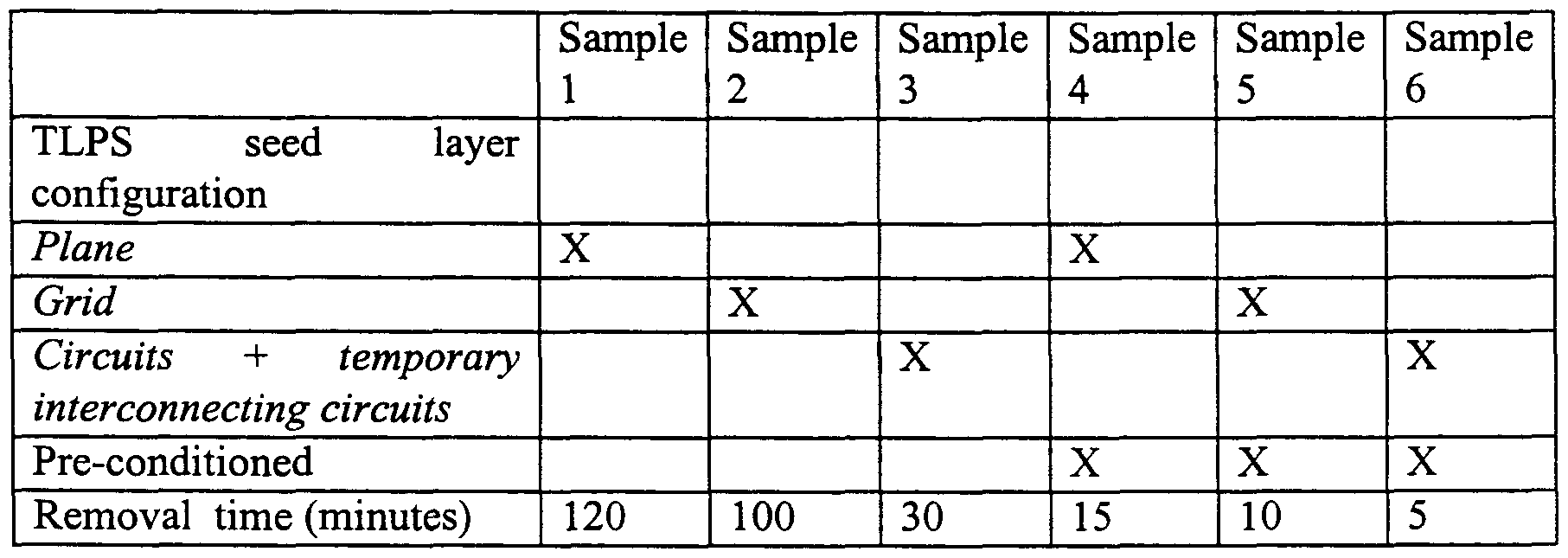
The purpose of this experiment was to determine: 1) the effects of patterning the TLPS seed layer on the speed of the TLPS removal process, and 2) the effects of a chemical precondictioning of the TLPS on the same. A six inch by six inch single layer circuit was fabricated on a polymeric substrate as in Example 1. The circuit bore traces that were 0.010-0.020 inches in width on average. Thus, approximately thirty percent of the surface of the substrate was covered by circuitry. The removal of the unplated portions of the TLPS seed layer was effected by a pressurized, directed stream of an abrasive filled slurry in a batch-type piece of equipment. The pressure of the slurry stream was maintained at 60 psi and the stream was manually directed over the surface of the substrate. A single operator was used to perform all of the tests. When subject to chemical preconditioning prior to mechanical removal, the preconditioning demonstrated no deleterious effects on the circuit. These results are summarized in the following table.
Thus, the most efficient removal of excess TLPS material is obtained by applying the TLPS in the pattern of the desired circuitry and then preconditioning the TLPS prior to mechanical removal.
While the invention has been described in detail with reference to certain preferred embodiments thereof, it will be understood that modifications and variations are within the scope and spirit of that which is described and claimed.