明 細 画 像 形 成 装 置 Detailed image forming device
< 技術分野 > <Technology>
本発明 は レ ー ザ一 ビー ム の走査 に よ っ て像担持体上 に 潜像を形成す る 画像形成装置 に関す る 。 The present invention relates to an image forming apparatus that forms a latent image on an image carrier by scanning a laser beam.
< 背景技術 > <Background technology>
従来、 レ ー ザ一 ビー ム に よ り 像担持体上に 静電潜像を 形成 し 、 電子写真プ ロ セ ス に よ り 紙上に高速 に 印刷を行 な う 画像形成装置力《、 コ ン ピ ュ ー タ 、 フ ァ ク シ ミ リ 、 多 機能複写機等の 出力装置 と し て広 く 用 い ら れて き た。 そ し て、 近年、 出力速度の 向上がよ り 一層望 ま れ、 そ の改 良が進んで い る Conventionally, an image forming apparatus capable of forming an electrostatic latent image on an image carrier by a laser beam and printing at high speed on paper by an electrophotographic process. It has been widely used as an output device for computers, facsimiles, multifunction copiers, and the like. In recent years, further improvements in output speed have been desired, and improvements have been made.
例え ば回転多面鏡型偏向装置を用 い た画像形成装置で は、 そ の鏡面の小面の 1 つ に つ き 1 本の レ ー ザー ビー ム を偏向 さ せて 1 本の走査線を描 く の で、 単位時間当 り の 走査数を増加 さ せ る に は、 回転多面鏡の小面の数が一定 の場合、 そ の 回転数が大 き く な る 。 逆に 回転数が一定の 場合 に は、 回転多面鏡の面数が增加す る 。 回転多面鏡の 回転数を增加 さ せ る に は、 気体 ま た は液体の動圧 ま た は 静圧を利用 し た軸受が必要 と な る が、 こ れ ら の軸受 は高 価で取扱が難 し く 一般的な レ ー ザ一 ビー ム プ リ ン 夕 に用 い る こ と は困難であ っ た。 逆 に 多面鏡の面数を增加 さ せ
る と 、 偏向角が小さ く な る の で、 偏向装置以降の光路長 が長 く な る 。 ま た結像光学系に入射す る レ ー ザ一.ビー ム の コ リ メ 一 ト 径が光路長 に比例 し て大 き く な り 、 レ ン ズ や回転多面鏡の大 き さ も大 き く な る 。 特に、 高い解像度 が要求 され る 場合は、 走査線の数が増え る た め、 よ り 大 き い回転数と 、 長い光路長が必要と な る 。 こ の こ と は、 偏向装置 に回転多面鏡以外の も の を用 い る 場合で も 同様 の現象であ り 、 走査周波数の増大 と 、 偏向装置以降の光 路長の増加を も た らす。 そ の た め一度の走査で、 複数の レ ー ザー ビー ム を用 い て複数の走査線を書 き 込む (い わ ゆ る マルチ ビー ム) 露光方法が開発さ れてい る 。 For example, in an image forming apparatus using a rotating polygon mirror type deflector, one laser beam is deflected to one of the small surfaces of the mirror surface to draw one scanning line. Therefore, in order to increase the number of scans per unit time, if the number of facets of the rotary polygon mirror is constant, the number of rotations increases. Conversely, when the rotation speed is constant, the number of surfaces of the rotating polygon mirror increases. Increasing the number of revolutions of a rotating polygon mirror requires bearings that use the dynamic pressure or static pressure of gas or liquid, but these bearings are expensive. Difficult to use for the general laser beam evening. Conversely, increase the number of faces of the polygon mirror In this case, the deflection angle becomes smaller, so that the optical path length after the deflection device becomes longer. In addition, the diameter of the laser beam incident on the imaging optical system increases in proportion to the optical path length, and the size of the lens and the rotating polygon mirror also increase. It will be better. In particular, when high resolution is required, the number of scanning lines is increased, so that a higher rotation speed and a longer optical path length are required. This is the same phenomenon even when a deflecting device other than a rotary polygon mirror is used, which causes an increase in the scanning frequency and an increase in the optical path length after the deflecting device. . Therefore, an exposure method has been developed in which multiple scanning lines are written using multiple laser beams in a single scan (so-called multi-beam).
複数の レ ー ザ一 ビー ム を得 る た め に は、 複数の ガス レ 一ザ一 (例え ば、 H e — N e ) 発振器を光源 と し て用 い た り 、 1 つ の発振器の レ ー ザー ビー ム を音響光学変調器 C A 0 M ) な どで時分割的 に複数に振 り 分け た り す る 方 法 も 開発 さ れたが、 よ り 簡潔で装置が小型に な る 方法 と し て、 例え ば特開昭 5 4 — 7 3 2 8 に示すよ う に、 1 つ の素子上に複数の レ ー ザ一 ビー ム射出用発光部を集積 し た 、 半導体 レ ー ザー ア レ イ が光源 と し て用 い ら れ る よ う に な っ て き た。 In order to obtain multiple laser beams, multiple gas laser (for example, He—Ne) oscillators can be used as the light source, or a single oscillator can be used. A method of distributing the laser beam into multiple pieces in a time-division manner using an acousto-optic modulator (CA0M) has also been developed.However, a simpler and more compact method has been developed. As shown in, for example, Japanese Patent Application Laid-Open No. 54-73228, a semiconductor laser array in which a plurality of laser beam emitting units are integrated on one element. A has come to be used as a light source.
半導体 レ ー ザー ァ レ イ を用 い た画像形成装置 につ い て 以下説明す る 。 画像形成 S は、 1 つ の基板上に集積 さ れた レ ー ザ一 ア レ イ を光源 と し て用 い てお り 、 各発光部 の ビー ム放射点は半導体の素子基板の端面に あ る 。 複数
の レ ー ザー ビー ム は共通の コ リ メ ー タ レ ン ズ に よ っ て各 々 略一定の 直径を持つ レ ー ザー ビー ム に コ リ メ 一 卜 さ れ 回転多面鏡 (偏向装置) の 1 つ の小面に入射す る 。 こ こ で小面の 回転に伴 っ て、 レ ー ザ— ビー ム は偏向 さ れ、 結 像 レ ン ズを経由 し てス ポ ッ 卜 に集束 さ れ、 像担持体を露 光 し て静電潜像が形成 さ れ る 。 形成 さ れた静電潜像 は、 電子写真プ ロ セ ス に従 っ て、 現像 さ れ紙の上に転写 さ れ 最後 に定着が行な われ る 。 ま た 、 特開昭 5 4 — An image forming apparatus using a semiconductor laser array will be described below. The image formation S uses a laser array integrated on one substrate as a light source, and the beam emission point of each light emitting unit is located on an end face of a semiconductor element substrate. . Multiple The laser beams are collimated into laser beams each having a substantially constant diameter by a common collimator lens, and are rotated by a polygonal mirror (deflecting device). Incident on one facet. Here, as the facet rotates, the laser beam is deflected, is focused on the spot via the imaging lens, and exposes the image carrier to become static. An electrostatic latent image is formed. The formed electrostatic latent image is developed, transferred to paper, and finally fixed according to an electrophotographic process. Also, Japanese Patent Laid-Open No. 54-54
1 5 8 2 5 1 に示 さ れて い る よ う に 、 像担持体上で同時 に走査す る 走査線の 間隔を小 さ く す る た め、 レ ー ザー ァ レ イ の発光部は走査面に対 し て あ る 角度を持 っ て配置 さ れ て い る 。 As shown in Fig. 1 58 2 51, the light emitting part of the laser array is designed to reduce the interval between the scanning lines that are simultaneously scanned on the image carrier. It is arranged at an angle to the scanning plane.
他方、 こ の よ う な半導体 レ ー ザ一 ア レ イ を用 い た画像 形成装置 に対 し 、 従来か ら 高速かつ高解像度の走査を行 な う こ と がで き る 画像形成装置が求め ら れて い る 。 し か し なが ら 従来の画像形成装置で は、 高速かつ高解像度の 走査を十分実現す る こ と がで き な い のが実情であ る 。 < 発明の開示 > On the other hand, for an image forming apparatus using such a semiconductor laser array, an image forming apparatus capable of performing high-speed and high-resolution scanning has been required. I'm afraid. However, it is a fact that conventional image forming apparatuses cannot sufficiently realize high-speed and high-resolution scanning. <Disclosure of Invention>
本発明 は こ の よ う な点を考慮 し て な さ れた も のであ り 高速かつ高解像度の レ ー ザー ビ一ム走查を行な う こ と が で き る と と も に 、 コ ン ノ、° ク ト な 画像形成装置を提供す る こ と を 目 的 と す る 。 The present invention has been made in consideration of the above points, and is capable of performing a high-speed and high-resolution laser beam drive. It is an object of the present invention to provide an image forming apparatus that is notorious and secure.
本発明 の第 1 の特徴は、 表面 に静電潜像が形成 さ れ る 像担持体 と 、 こ の像担持体の表面を帯電 さ せ る 帯電器 と
帯電 し た前記像担持体の表面に対 し て複数の レ ー ザー ビ ー 厶 を走査す る レ ー ザー ビー ム 走査装置 と 、 レ ー ザー ビ ー ムが走査 さ れた前記像担持体の表面に現像剤を付着 さ せ る現像器 と を備え、 前記 レ ー ザー ビー ム走査装置 は素 子基板上に レ ー ザー ビー ム の発光部が複数形成 さ れた半 導体 レ ー ザ一 ア レ イ と 、 前記発光部か ら の レ ー ザー ビー ム を前記像担持体の表面へ偏向 さ せ る 偏向装置 と を有 し 、 前記発光部は前記半導体 レ ー ザー ァ レ イ 表面に 2 次元状 に配置 さ れる と と も に、 各発光部は個別に そ の点灯お よ び光量が制御可能であ る こ と を特徴 と す る 画像形成装置 ■あ る。 A first feature of the present invention is that an image carrier having an electrostatic latent image formed on a surface thereof, and a charger for charging the surface of the image carrier are provided. A laser beam scanning device that scans a plurality of laser beams on the charged surface of the image carrier, and a laser beam scanning device that scans the laser beam. A developing device for adhering a developer to the surface, wherein the laser beam scanning device is a semiconductor laser area having a plurality of laser beam emitting portions formed on a substrate. And a deflecting device for deflecting a laser beam from the light emitting section toward the surface of the image carrier, wherein the light emitting section is two-dimensionally arranged on the surface of the semiconductor laser array. There is an image forming apparatus which is characterized in that each of the light-emitting portions can be individually controlled in terms of lighting and light amount while being arranged in a shape.
本発明の第 2 の特徴は、 素子基板上に レ ー ザー ビー ム の発光部が複数形成 さ れた半導体 レ ー ザー ア レ イ と 、 前 記発光部か ら の レ ーザ一 ビー ム を偏向 さ せ る 偏向装置 と を有 し 、 前記発光部は前記半導体ア レ イ 表面に 2 次元状 に配置 さ れ る と と も に、 各発光部は個別に そ の点灯お よ び光量が制御可能 と な っ てい る こ と を特徴 と す る レ ー ザ 一 ビー ム 走査装置であ る 。 A second feature of the present invention is that a semiconductor laser array in which a plurality of light emitting portions of a laser beam are formed on an element substrate, and a laser beam from the light emitting portion are provided. A deflecting device for deflecting light, wherein the light emitting units are arranged two-dimensionally on the surface of the semiconductor array, and each light emitting unit is individually controlled for its lighting and light amount. A laser beam scanning device characterized in that it can be used.
本発明の第 3 の特徴は、 表面に静電潜像が形成 さ れる 像担持体 と 、 こ の像担持体の表面を帯電 さ せ る 帯電器 と 、 帯 ¾ し た前記像担持体の表面に対 し て複数の レ ー ザー ビ ー ム を走査す る レ ー ザー ビー ム走査装置 と 、 レ ー ザー ビ ― ムが走査 さ れた前記像担持体の表面に現像剤を付着 さ せ る 現像器 と を備え 、 前記 レ ー ザー ビー ム走査装置 は素
子基板上に レ ー ザー ビ ー ム の発光部が形成 さ れた半導体 レ ー ザー と 、 前記発光部か ら の レ ー ザー ビ ー ム を前記像 担持体の表面へ偏向 さ せ る 偏向装置 と を有 し 、 前記発光 部 は前記素子基板面 に対 し 略垂直な光軸を有す る こ と を 特徴 と す る 画像形成装置であ る 。 A third feature of the present invention is that an image carrier on which an electrostatic latent image is formed, a charger for charging the surface of the image carrier, and a band-like surface of the image carrier A laser beam scanning device for scanning a plurality of laser beams with respect to the laser beam, and applying a developer to the surface of the image carrier on which the laser beam has been scanned. And a laser beam scanning device. A semiconductor laser having a laser beam emitting portion formed on a daughter substrate; and a deflecting device for deflecting the laser beam from the light emitting portion toward the surface of the image carrier. Wherein the light emitting section has an optical axis substantially perpendicular to the element substrate surface.
本発明 の第 4 の特徴は、 素子基板上 に レ ー ザー ビ ー ム の発光部が形成 さ れた半導体 レ ー ザー と 、 前記発光部か ら の レ ー ザ— ビ ー ム を偏向 さ せ る 偏向装置 と を有 し 、 前 記発光部 は前記素子基板面 に対 し 略垂直な光軸を有す る こ と を特徴 と す る レ ー ザ一 ビ ー ム走査装置であ る 。 A fourth feature of the present invention is that a semiconductor laser in which a light emitting portion of a laser beam is formed on an element substrate, and that the laser beam from the light emitting portion is deflected. And a deflecting device, wherein the light emitting section has an optical axis substantially perpendicular to the element substrate surface.
本発明 の第 5 の特徴は、 表面に静電潜像が形成 さ れ る 像担持体 と 、 こ の像担持体の表面を帯電 さ せ る 帯電器 と 、 帯電 し た像担持体の表面 に対 し て複数の レ ー ザ ー ビー ム を走査す る レ ー ザー ビー ム走査装置 と 、 レ ー ザー ビー ム が走査 さ れた像担持体の表面 に現像剤を付着 さ せ る 現像 器 と を備え 、 前記 レ ー ザー ビ ー ム走査装置 は複数の レ ー ザ一 ビー ム を射出す る 半導体 レ ー ザー ア レ イ と 、 前記複 数の レ ー ザー ビ ー ム の各 々 を平行化す る コ リ メ 一 夕 レ ン ズ と 、 前記 コ リ メ ー タ ー レ ン ズで平行化 さ れた複数の レ — ザ一 ビー ム の方向 を周期的 に偏向す る 偏向装置 と 、 前 記偏向装置 に よ っ て偏向 さ れた レ ー ザ一 ビ ー ム を前記像 担持体上 に結像 さ せ る 走査 レ ン ズ と を有 し 、 前記偏向装 置 は 1 つ の反射面を有す る 回転鏡で あ る こ と を特徴 と す る 画像形成装置であ る 。
本発明の第 6 の特徴は、 複数の レ ー ザー ビー ム を射出 す る 半導体 レ ー ザー ア レ イ と 、 前記複数の レ ー ザー ビ一 ム の各々 を平行化す る コ リ メ 一 夕 レ ン ズ と 、 前記 コ リ メ 一 タ一 レ ン ズで平行化 さ れた複数の レ ー ザー ビー ム の方 向を周期的に偏向す る 偏向装置 と 、 前記偏向装置に よ つ て偏向 さ れた レ ー ザ一 ビー ム を像担持体上に結像 さ せ る 走査 レ ン ズ と を有 し 、 前記偏向装置は 1 つ の反射面を有 す る 回転鏡であ る こ と を特徴 と す る レ ー ザー ビー ム走査 装置であ る 。 A fifth feature of the present invention is that an image carrier having an electrostatic latent image formed on the surface thereof, a charger for charging the surface of the image carrier, and a surface of the charged image carrier are provided. A laser beam scanning device for scanning a plurality of laser beams, and a developing device for applying a developer to the surface of the image carrier on which the laser beam has been scanned. The laser beam scanning device parallelizes a semiconductor laser array that emits a plurality of laser beams and each of the plurality of laser beams. A deflecting device for periodically deflecting the direction of a plurality of laser beams collimated by the collimator lens; Forming a laser beam deflected by the deflecting device on the image carrier; A scanning lens, and the deflecting device is a rotating mirror having one reflecting surface. A sixth feature of the present invention is that a semiconductor laser array for emitting a plurality of laser beams and a collimator array for parallelizing each of the plurality of laser beams are provided. Lens, a deflecting device for periodically deflecting the direction of the plurality of laser beams collimated by the collimator lens, and a deflecting device for deflecting by the deflecting device. A scanning lens for forming an image of the laser beam on the image carrier, and the deflecting device is a rotating mirror having one reflecting surface. It is a laser beam scanning device.
本発明の第 7 の特徴は、 表面に静電潜像が形成 さ れ る 像担持体 と 、 こ の像担持体の表面を帯電 さ せ る 帯電器 と 、 帯電 し た像担持体の表面に対 し て複数の レ ー ザ一 ビー ム を走査す る レ ー ザ一 ビー ム走査装置 と 、 レ ー ザ一 ビー ム が走査 さ れた像担持体の表面に現像剤を付着 さ せ る 現像 器 と を備え、 前記 レ ー ザ一 ビー ム走査装置は レ ー ザー ビ ー ム を射出する発光部を複数有す る半導体 レ ー ザー ァ レ ィ と 、 前記複数の レ ー ザー ビー ム の各々 を平行化す る コ リ メ 一 夕 レ ン ズ と 、 前記 コ リ メ ー タ ー レ ン ズで コ リ メ 一 ト さ れた複数の レ ー ザ一 ビー ム の方向を周期的 に偏向す る 偏向装置 と 、 前記偏向装置 に よ っ て偏向 さ れた レ ー ザ 一 ビー ム を前記像担持体上に結像 さ せ る 走査 レ ン ズ と を 有 し 、 前記 コ リ メ 一 タ レ ン ズの焦点距離を f c 、 前記半 導体 レ ー ザ一 ア レ イ 上の複数の発光部の う ち 、 相互の距 離の最 も遠い 2 つ の発光部の 間隔を <5 m a x と す る と 、
f c / δ m a x > 2 5 A seventh feature of the present invention is that an image carrier on which an electrostatic latent image is formed on a surface, a charger for charging the surface of the image carrier, and a surface of the charged image carrier are provided. A laser beam scanning device for scanning a plurality of laser beams, and a developing device for applying a developer to the surface of the image carrier on which the laser beam has been scanned. A laser beam scanning device comprising: a semiconductor laser array having a plurality of light-emitting portions for emitting a laser beam; and each of the plurality of laser beams. And a plurality of laser beams collimated by the collimator lens are periodically deflected. A deflecting device and a laser beam deflected by the deflecting device are formed on the image carrier. A scanning lens having a focal length of the collimator lens, fc, and a mutual distance among a plurality of light emitting portions on the semiconductor laser array. If the distance between the two furthest emitting parts is <5 max, then fc / δ max> 2 5
であ る こ と を特徴 と す る 画像形成装置であ る 。 An image forming apparatus characterized in that:
本発明 の第 8 の特徴は、 レ ー ザー ビ ー ム を射出す る 発 光部を複数有す る 半導体 レ ー ザー ア レ イ と 、 前記複数の レ ー ザー ビー ム の各 々 を平行化す る コ リ メ ー タ レ ン ズ と 、 前記 コ リ メ ー タ レ ン ズで コ リ メ ー ト さ れた複数の レ ー ザ 一 ビー ム の方向 を周期的 に偏向す る 偏向装置 と 、 前記偏 向装置 に よ っ て偏向 さ れた レ ー ザ ー ビー ム を前記像担持 体上に結像 さ せ る 走査 レ ン ズ と を備え 、 前記 コ リ メ ー タ レ ン ズの焦点位置を f c 、 前記半導体 レ ー ザ 一 ア レ イ 上 の複数の発光部の う ち 、 相互の距離の最 も遠い 2 つ の発 光部の 間隔を 5 m a X と す る と 、 An eighth feature of the present invention is that a semiconductor laser array having a plurality of light emitting portions for emitting a laser beam and each of the plurality of laser beams is parallelized. A collimator lens; a deflecting device for periodically deflecting a direction of a plurality of laser beams collimated by the collimator lens; A scanning lens for forming a laser beam deflected by the deflecting device on the image carrier, and a focus position of the collimator lens. Where fc is the distance between the two light emitting parts, which are farthest from each other, of the plurality of light emitting parts on the semiconductor laser array, and
f c / δ m a X > 2 5 f c / δ m a X> 25
であ る こ と を特徴 と す る レ ー ザー ビ ー ム走査装置であ る 。 The laser beam scanning device is characterized in that:
本発明 の第 9 の特徴は、 表面に静電潜像が形成 さ れ る 像担持体 と 、 こ の像担持体の表面を帯電 さ せ る 帯電器 と 、 帯電 し た像担持体の表面に対 し て複数の レ ー ザー ビー ム を走査す る レ ー ザー ビ ー ム走査装置 と 、 レ ー ザ一 ビ ー ム が走査 さ れた像担持体の表面に現像剤を付着 さ せ る 現像 器 と を備え 、 前記 レ ー ザー ビ ー ム走査装置 は レ ー ザ一 ビ ー ム を射出す る 複数個の発光部が素子基板上に設け ら れ た半導体 レ ー ザー ア レ イ と 、 前記発光部か ら 射出 さ れ る レ ー ザー ビ ー ム を偏向す る te向装置 と を有 し 、 前記半導 体 レ ー ザ 一 ァ レ イ カ、 ら射出 さ れ る レ ー ザ ー ビ ー ム の 中心
軸は、 前記素子基板面に対 し て略垂直であ り 、 前記半導 体 レ ー ザー ア レ イ と 前記偏向装置 と の間の光路上に おい て、 複数の レ ー ザー ビー ム の断面の少な く と も一部が重 な り 合 う 位置に開口絞 り を設け、 前記開 口絞 り を通過 し た後の複数の レ ー ザー ビー ム の う ち 、 パ ワ ーが最大であ る レ ー ザ一 ビー ム につ い て、 そ の パ ワ ー を 1 と し た と き に 、 そ の他の レ ー ザー ビー ム の ' ヮ 一 が各 々 0 . 9 以上 と な る こ と を特徴とする 画像形成装置であ る 。 A ninth feature of the present invention is that an image carrier having an electrostatic latent image formed on the surface thereof, a charger for charging the surface of the image carrier, and a surface of the charged image carrier are provided. A laser beam scanning device for scanning a plurality of laser beams, and a developing device for applying a developer to the surface of the image carrier on which the laser beam has been scanned. A laser beam scanning device, wherein the laser beam scanning device has a plurality of light-emitting portions for emitting a laser beam, the plurality of light-emitting portions being provided on an element substrate; and have a te direction device and you deflect the record over Heather bi chromatography beam that will be emitted or light-emitting portion, et al., the semiconductors les chromatography the one § les squid, Les chromatography the chromatography bicycloalkyl over that will be al injection The center of the The axis is substantially perpendicular to the surface of the element substrate, and is a cross section of a plurality of laser beams on an optical path between the semiconductor laser array and the deflecting device. An aperture stop is provided at a position where at least a part of the laser beam overlaps, and the power of the laser beam after passing through the aperture stop is the largest. When the power of a laser beam is set to 1 and the other laser beams have a height of 0.9 or more, respectively. An image forming apparatus characterized by the following.
本発明の第 1 0 の特徴は、 レ ーザー ビー ム を射出す る 複数個の発光部が素子基板上に設け ら れた半導体 レ ー ザ 一ア レ イ と 、 前記発光部か ら射出 さ れ る レ ー ザー ビー ム を偏向す る偏向装置 と を有 し 、 前記半導体 レ ー ザー ァ レ ィ か ら射出 さ れる レ ー ザー ビー ム の 中心軸は、 前記素子 基板面に対 し て略垂直であ り 、 前記半導体 レ ー ザー ァ レ ィ と 前記偏向装置 と の間の光路に おい て、 複数の レ ー ザ 一 ビー ム の断面の少な く と も一部が重な り 合 う 位置に開 口絞 り を設け、 前記開口絞 り を通過 し た後の複数の レ ー ザ一 ビー ム の う ち 、 パ ワ ーが最大であ る レ ーザ一 ビー ム につ いて、 そ の ° ヮ一を 1 と し た と き に、 そ の他の レ 一 ザ一 ビー ム のパ ワ ーが各々 0 . 9 以上 と な る こ と を特徴 と す る レ ー ザ一 ビー ム走査装置であ る 。 A tenth feature of the present invention resides in that a semiconductor laser array in which a plurality of light emitting portions for emitting a laser beam are provided on an element substrate, and which are emitted from the light emitting portion. A deflecting device for deflecting the laser beam, wherein a central axis of the laser beam emitted from the semiconductor laser array is substantially perpendicular to the element substrate surface. And in the optical path between the semiconductor laser array and the deflecting device, at a position where at least a part of the cross section of the plurality of laser beams overlaps. An aperture is provided, and the laser beam having the largest power out of a plurality of laser beams after passing through the aperture is used. When the number is set to 1, the power of other laser beams is 0.9 or more each. A laser beam scanning device characterized by the following characteristics.
本発明の第 1 1 の特徴は、 表面に静電潜像が形成 さ れ る 像担持体 と 、 こ の像担持体の表面を帯電 さ せ る 帯電器 と 、 帯電 し た像担持体の表面に対 し て複数の レ ー ザー ビ
— ム を走査す る レ ー ザー ビ ー ム走査装置 と 、 レ ー ザー ビ ー ム が走査 さ れた 像担持体の表面 に現像剤を付着 さ せ る 現像器 と を備え、 前記 レ ー ザ一 ビー ム走査装置 は レ ー ザ 一 ビー ム を射出す る 複数個の発光部を有す る 半導体 レ ー ザ一 ア レ イ と 、 前記発光部か ら 射出 さ れた レ ー ザ一 ビー ム を平行 ビ ー ム 化す る た め の コ リ メ ー タ レ ン ズ と 、 レ ー ザ一 ビ ー ム を偏向す る 偏向装置を有 し 、 前記半導体 レ ー ザー ァ レ イ と 前記偏向装置 と の 間 の光路上 に 開 口絞 り 力く 設け ら れ、 前記 コ リ メ ー タ レ ン ズの焦点距離を f 、 前記 コ リ メ 一 夕 レ ン ズの前記偏向装置側の焦点 と 前記開 口絞 り と の 間隔を s 、 前記 コ リ メ 一 タ レ ン ズの光軸力、 ら 最 も 離れた位置 に配置 さ れた発光部 と 前記光軸 と の 間隔を t 、 前記開 口絞 り の 直径を D 、 前記平行 ビ ー ム の 直径を d と す る と き 、 A first feature of the present invention is that an image carrier having an electrostatic latent image formed on a surface thereof, a charger for charging the surface of the image carrier, and a surface of the charged image carrier are provided. Multiple lasers A laser beam scanning device that scans a laser beam; and a developing device that causes a developer to adhere to the surface of the image carrier on which the laser beam has been scanned. A beam scanning device includes a semiconductor laser array having a plurality of light emitting units for emitting a laser beam, and a laser beam emitted from the light emitting unit. A collimator lens for converting the laser beam into a parallel beam, and a deflecting device for deflecting the laser beam, wherein the semiconductor laser array, the deflecting device, The focal length of the collimator lens is f, the focal point of the collimator lens on the deflecting device side and the aperture is The distance from the aperture is s, the optical axis force of the collimator lens, the position farthest from the aperture When the distance between the light emitting portion arranged in the optical axis and the optical axis is t, the diameter of the aperture stop is D, and the diameter of the parallel beam is d,
s t / D 、 2 · 3 st / D, 2 · 3
≤ 0 . 1 2 + 0 . 1 7 ≤ 0 .1 2 + 0 .1 7
f d ノ f d no
D D
9 9
d な る 条件を満足す る こ と を特徴 と す る 画像形成装置であ る o d An image forming apparatus characterized by satisfying certain conditions o
本発明 の第 1 2 の特徴は、 表面 に静電潜像が形成 さ れ る 像担持体 と 、 こ の像担持体の表面を帯電 さ せ る 帯電器 と 、 帯電 し た像担持体の表面 に対 し て複数の レ ー ザー ビ ー ム を走査す る レ ー ザ一 ビー ム 走査装置 と 、 レ ー ザ一 ビ
0 ー ムが走査 さ れた像担持体の表面に現像剤を付着 さ せ る 現像器 と を備え、 前記 レ ー ザー ビ ー ム走査装置は レ ー ザ 一 ビー ム を射出す る複数個の発光部を有する 半導体 レ ー ザ一 ア レ イ と 、 前記発光部か ら射出 さ れた レ ー ザ一 ビー ム を平行 ビー ム 化す る た めの コ リ メ ー タ レ ン ズ と 、 レ ー ザ一 ビー ム を偏向す る 偏向装置 と を有 し 、 前記半導体 レ 一 ザ一 ァ レ イ と前記偏向装置 と の 間の光路上に開 口絞 り が設け ら れ、 前記 コ リ メ ー タ レ ン ズ の焦点距離を f 、 前 記 コ リ メ 一 夕 レ ン ズ の前記儒向装置側の焦点 と 前記開 口 絞 り と の間隔を s 、 前記 コ リ メ ー タ レ ン ズ の光軸か ら最 も離れた位置に配置 さ れた発光部 と前記光軸 と の 間隔を t 、 前記開口絞 り の直径を D 、 前記平行 ビー ム の直径を d と す る と き 、
A twenty-second feature of the present invention is that an image carrier having an electrostatic latent image formed on a surface thereof, a charger for charging the surface of the image carrier, and a surface of the charged image carrier are provided. Laser beam scanning device that scans a plurality of laser beams for laser beam, and laser beam scanning device And a developing device for applying a developing agent to the surface of the image carrier on which the beam has been scanned, wherein the laser beam scanning device includes a plurality of laser beam ejecting units. A semiconductor laser array having a light-emitting portion, a collimator lens for converting the laser beam emitted from the light-emitting portion into a parallel beam, and a laser. A deflecting device for deflecting the beam, wherein an aperture is provided on an optical path between the semiconductor laser array and the deflecting device, wherein the collimator is provided. The focal length of the lens is f, the distance between the focal point on the side of the collimating lens and the aperture stop is s, and the light of the collimator lens is The distance between the light-emitting portion arranged farthest from the axis and the optical axis is t, and the diameter of the aperture stop is D, where d is the diameter of the parallel beam,
D D
つ One
d な る 条件を満足す る こ と を特徴と す る 画像形成装置であ 本発明の第 1 3 の特徴は、 レ ー ザー ビー ム を射出す る 複数個の発光部を有す る 半導体 レ ー ザー ア レ イ と 、 前記 発光部か ら射出 さ れた レ ー ザー ビ ー ム を平行 ビ ー ム 化す る た めの コ リ メ 一 夕 レ ン ズ と 、 レ ー ザー ビー ム を偏向す る 偏向装置 と を有 し 、 前記半導体 レ ー ザー ア レ イ と前記
1 d An image forming apparatus characterized by satisfying certain conditions. A thirteenth feature of the present invention is that a semiconductor laser having a plurality of light emitting portions for emitting a laser beam is provided. Laser beam, laser beam emitted from the light-emitting section, and a collimation lens for converting the laser beam into a parallel beam, and the laser beam are deflected. A deflecting device, and the semiconductor laser array and the deflecting device. 1
偏向装置 と の 間の光路上に開 口絞 り が設け ら れ、 前記 コ リ メ 一 夕 レ ン ズの焦点距離を f 、 前記 コ リ メ 一 タ レ ン ズ の前記偏向装置側の焦点 と 前記開 口絞 り と の 間隔を s 、 前記 コ リ メ 一 タ レ ン ズの光軸か ら最 も離れた位置 に配置 さ れた発光部 と 前記光軸 と の 間隔を t 、 前記開 口絞 り の 直径を D 、 前記平行 ビ ー ム の 直径を d と す る と き 、 s t D 2 . 3 An aperture stop is provided on the optical path between the lens and the deflecting device. The focal length of the collimator lens is f, and the focal length of the collimator lens on the deflecting device side is The distance between the aperture stop and the aperture is s, the distance between the light-emitting unit disposed farthest from the optical axis of the collimator lens and the optical axis is t, and the distance between the aperture and the aperture is t. When the diameter of the aperture is D and the diameter of the parallel beam is d, st D2.3
≤ 0 2 + 0 1 7 ≤ 0 2 + 0 1 7
d d
D D
2 Two
d な る 条件を満足す る こ と を特徴 と す る レ ー ザ一 ビ ー ム走 查装置であ る d A laser beam driving device characterized by satisfying certain conditions
本発明 の第 1 4 の特徵 は 、 レ ー ザ一 ビ ー ム を射出す る 複数個の発光部を有す る 半導体 レ ー ザ一ア レ イ と 、 前記 発光部か ら射出 さ れた レ ー ザ一 ビ ー ム を平行 ビ ー ム 化す る た め の コ リ メ ー タ レ ン ズ と 、 レ ー ザ一 ビ ー ム を偏向す る 偏向装置 と を有 し 、 前記半導体 レ ー ザー ァ レ ィ と 前記 偏向装置 と の 間の光路上 に開 口絞 り が設け ら れ、 前記 コ リ メ 一 夕 レ ン ズの焦点距離を f 、 前記 コ リ メ 一 夕 レ ン ズ の前記偏向装置側の焦点 と 前記開 口絞 り と の 間隔を s 、 前記 コ リ メ 一 タ レ ン ズの光奉田力、 ら 最 ち 離れた位置 に配置 さ れた発光部 と 前記光軸 と の 間隔を t 、 前記開 口絞 り の 直径を D 、 前記平行 ビ一ム の 直径を d と す る と さ 、
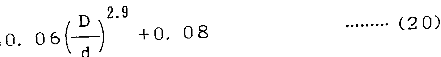
s t D · 9 A fourteenth feature of the present invention is that a semiconductor laser array having a plurality of light emitting portions for emitting a laser beam, and a laser beam emitted from the light emitting portion. A collimator lens for converting the laser beam into a parallel beam; and a deflecting device for deflecting the laser beam. An aperture is provided on the optical path between the ray and the deflecting device, the focal length of the collimation lens is f, and the deflecting device of the collimation lens is The distance between the focal point on the side and the aperture stop is s, the distance between the light emitting unit arranged farthest from the collimator lens and the optical axis, and the distance between the light axis and the optical axis. t, the diameter of the aperture stop is D, and the diameter of the parallel beam is d, st D · 9
≤ 0 . 0 6 + 0 . 0 8 ≤ 0 .06 + 0 .0 8
f 、 d ノ f, d
D D
≤ 2 ≤ 2
d な る 条件を満足す る こ と を特徴 と す る レ ー ザ一 ビー ム走 查装置であ る 。 d A laser beam running device characterized by satisfying certain conditions.
< 図面の簡単な 説明 > <Brief description of drawings>
図 1 は本発明 に よ る 画像形成装置の第 1 の実施例を示 す レ ー ザー走査光学系の概略図、 FIG. 1 is a schematic view of a laser scanning optical system showing a first embodiment of an image forming apparatus according to the present invention,
図 2 は画像形成装置を示す側面図、 FIG. 2 is a side view showing the image forming apparatus,
図 3 は面発光型半導体 レ ー ザー ァ レ イ の光共振器の断 面図、 Figure 3 is a cross-sectional view of an optical resonator of a surface-emitting type semiconductor laser array.
図 4 は位相同期の面発光型半導体 レ ー ザー ァ レ イ の発 光部を示す斜視図、 FIG. 4 is a perspective view showing a light emitting unit of a phase-locked surface-emitting type semiconductor laser array.
図 5 は走査線に対す る ス ポ ッ 卜 位置の関係を示す配置 図、 Figure 5 is a layout diagram showing the relationship of the spot position to the scanning line.
図 6 は位相同期の面発光型半導体 レ ー ザー ア レ イ の発 光部の光共振器の配置図、 Figure 6 shows the layout of the optical resonator in the light-emitting section of a phase-locked surface-emitting semiconductor laser array.
図 7 は一般的な端面発光型半導体 レ ー ザ— ア レ イ の概 念図、 Figure 7 is a schematic diagram of a general edge emitting semiconductor laser array.
図 8 は一般的な レ ー ザ走査光学系の光路断面図、 図 9 は走査線に 対す る ス ポ ッ ト 位置の関係を示す配置 、
図 1 0 は一般的な金属 ミ ラ 一 の P 偏向 お よ び S 偏向 の 反射率を示す説明図、 FIG. 8 is an optical path cross-sectional view of a general laser scanning optical system, and FIG. 9 is an arrangement showing a relationship of a spot position with respect to a scanning line. Fig. 10 is an explanatory diagram showing the P-polarization and S-polarization reflectivity of a general metal mirror,
図 1 1 は レ ー ザ 一 ビ ー ム の コ リ メ ー ト 径の調整方法を 示す概略図、 Figure 11 is a schematic diagram showing how to adjust the collimation diameter of the laser beam.
図 1 2 は本発明 に よ る 画像形成装置の第 2 の実施例を 示す レ ー ザー走査光学系の概略図、 FIG. 12 is a schematic view of a laser scanning optical system showing a second embodiment of the image forming apparatus according to the present invention,
図 1 3 は画像形成装置を示す側面図、 FIG. 13 is a side view showing the image forming apparatus.
図 1 4 は面発光型半導体 レ ー ザ一 の光共振器の断面図 図 1 5 は位相 同期の面発光型半導体 レ ー ザー ア レ イ の 発光部を示す斜視図、 FIG. 14 is a cross-sectional view of an optical resonator of a surface-emitting type semiconductor laser. FIG. 15 is a perspective view showing a light-emitting portion of a phase-locked surface-emitting type semiconductor laser array.
図 1 6 は位相同期の面発光型半導体 レ ー ザー ア レ イ の 発光部の光共振器の配置図、 Figure 16 shows the layout of the optical resonator in the light-emitting section of a phase-locked surface-emitting semiconductor laser array.
図 1 7 は一般的な レ ー ザ走査光学系の走査線 と 直角 方 向の光軸断面図、 Fig. 17 is a cross-sectional view of the optical axis perpendicular to the scanning line of a general laser scanning optical system.
図 1 8 は一般的な半導体 レ ー ザ一 の概略図、 Figure 18 is a schematic diagram of a typical semiconductor laser.
図 1 9 は一般的な金属 ミ ラ ー の P 偏向 お よ び S 偏向 の 反射率を示す説明 図、 Fig. 19 is an explanatory diagram showing the reflectivity of a general metal mirror for P and S deflection.
図 2 0 は本発明 に よ る 画像形成装置の第 3 の実施例を 示す レ ー ザ走査光学系の概略図 FIG. 20 is a schematic diagram of a laser scanning optical system showing a third embodiment of the image forming apparatus according to the present invention.
図 2 1 は画像形成装置を示す側面図、 FIG. 21 is a side view showing the image forming apparatus.
図 2 2 は走査面内での光路断面図、 Figure 22 is a sectional view of the optical path in the scanning plane.
図 2 3 は面発光型半導体 レ ー ザ一 の光共振器の断面図 図 2 4 は走査線 に対す る ス ポ ッ ト 位置の関係を示す配 置図、
図 2 5 は ビー ム偏向装置の平面図、 FIG. 23 is a cross-sectional view of an optical resonator of a surface-emitting type semiconductor laser. FIG. 24 is a layout diagram showing a relationship of a spot position with respect to a scanning line. Figure 25 is a plan view of the beam deflecting device.
図 2 6 は一般的な回転多面鏡を用 い た ビ ー ム偏向装置 の作動図、 Figure 26 shows the operation of a beam deflecting device using a general rotating polygon mirror.
図 2 7 は一般的な レ ー ザー ビ ー ム走査光学系の光路断 面図、 Fig. 27 is a cross-sectional view of the optical path of a general laser beam scanning optical system.
図 2 8 は一般的な端面発光型半導体 レ ー ザー の概略図、 図 2 9 は本発明 に よ る 画像形成装置の第 4 の実施例を 示す レ ー ザー走査光学系の概略図、 FIG. 28 is a schematic diagram of a general edge-emitting semiconductor laser, FIG. 29 is a schematic diagram of a laser scanning optical system showing a fourth embodiment of the image forming apparatus according to the present invention,
図 3 0 は画像形成装置を示す側面図、 FIG. 30 is a side view showing the image forming apparatus,
図 3 1 は面発光型半導体 レ ー ザー の光共振器の断面図、 図 3 2 は走査線に対す る ス ポ ッ ト 位置の関係を示す配 置図、 FIG. 31 is a cross-sectional view of an optical resonator of a surface-emitting type semiconductor laser. FIG. 32 is a layout diagram showing a relationship of a spot position with respect to a scanning line.
図 3 3 は一般的な レ ー ザー ビ ー ム走査光学系の光路断 面図、 Fig. 33 is a cross-sectional view of the optical path of a general laser beam scanning optical system.
図 3 4 は一般的な マ ルチ ビー ム走査方式に お け る 光路 断面図、 Figure 34 is a cross-sectional view of the optical path in a general multi-beam scanning method.
図 3 5 は一般的な端面発光型半導体 レ ー ザー の概略図、 図 3 6 は一般的な倒れ補正 レ ン ズを含む光路断面図、 図 3 7 は本発明 に よ る 画像形成装置の第 5 の実施例を 示す レ ー ザー走査光学系の概略図、 FIG. 35 is a schematic diagram of a general edge-emitting semiconductor laser, FIG. 36 is a cross-sectional view of an optical path including a general tilt correction lens, and FIG. 37 is a diagram of an image forming apparatus according to the present invention. FIG. 5 is a schematic view of a laser scanning optical system showing the fifth embodiment;
図 3 8 は画像形成装置を示す側面図、 FIG. 38 is a side view showing the image forming apparatus.
図 3 は走査光学系 に お け る 光源付近の構成図、 図 4 0 は他の実施例を示す走査光学系にお け る 光源付 近の構成図、
図 4 1 は一般の走査光学系 に お け る 光源付近の構成図 . 図 4 2 は本発明 に よ る 画像形成装置の第 6 の実施例を 示す レ ー ザー 走査光学系の概略図、 FIG. 3 is a configuration diagram around a light source in a scanning optical system, FIG. 40 is a configuration diagram around a light source in a scanning optical system showing another embodiment, Fig. 41 is a block diagram showing the vicinity of a light source in a general scanning optical system, Fig. 42 is a schematic diagram of a laser scanning optical system showing a sixth embodiment of the image forming apparatus according to the present invention,
図 4 3 は一般の走査光学系 に お け る 光源付近の構成図、 図 4 4 は開 口 絞 り に よ っ て ビ ー ム 力 け ら れ る こ と を示 す説明図、 Fig. 43 is a diagram showing the configuration near the light source in a general scanning optical system, and Fig. 44 is an explanatory diagram showing that the beam power can be applied by the aperture stop.
図 4 5 は コ リ メ 一 夕 レ ン ズの焦点位置 に開 口 絞 り を設 け た場合の光線図、 Fig. 45 is a ray diagram when an aperture stop is set at the focal point of the lens.
図 4 6 は コ リ メ - タ レ ン ズの焦点位置か ら はずれた位 置 に開 口絞 り を設 け た場合の光線図、 Fig. 46 is a ray diagram when the aperture stop is set at a position off the focal point of the collimator lens.
図 4 7 は ビ ー ム 断面強度分布が け ら れ る 様子を示す図、 図 4 8 は画像形成装置を示す側面図、 FIG. 47 is a diagram showing how the beam cross-sectional intensity distribution is blurred. FIG. 48 is a side view showing the image forming apparatus.
図 4 9 は走査光学系 に お け る 光源付近の構成図。 Figure 49 is a configuration diagram near the light source in the scanning optical system.
く 発明 を実施す る た め の最良の形態 > BEST MODE FOR CARRYING OUT THE INVENTION>
§ 1 画像形成装置の第 1 の実施例 § 1 First embodiment of image forming apparatus
1 - 1 背景技術 と の対比 1-1 Comparison with background technology
本実施例を よ り 良 く 理解す る た め、 は じ め に背景技術 につ い て述べ る 。 In order to better understand the present embodiment, the background art will be described first.
画像形成装置 に用 い ら れて い る 一般的 な半導体 レ ー ザ 一ア レ イ を図 7 に示す。 図 7 に示す よ う に 、 レ ー ザー ビ — ム を射出す る 半導体 レ ー ザー ア レ イ 1 に お い て は、 レ 一ザ一 ビー ム の光軸を含み接合面 に平行な面 と 、 同 じ く 光軸を含み接合面 に垂直な面で は、 ビ ー ム の拡が り 角 力く 大 き く 異な っ て い た。 図 7 に お い て、 接合面に平行な 面
で の拡が り 角 θ ρ は通常の レ ー ザー ダイ ォ ー ドの場合、 半値全角で約 1 0 度に な る 。 と こ ろ が接合面に垂直な面 では拡が り 角 6 t は回析の影響を受け、 半値全角で約Fig. 7 shows a typical semiconductor laser array used for an image forming apparatus. As shown in FIG. 7, the semiconductor laser array 1 that emits a laser beam has a surface parallel to the bonding surface that includes the optical axis of the laser beam. Similarly, on a plane including the optical axis and perpendicular to the joint plane, the beam spread and the angular power was greatly different. In Fig. 7, the plane parallel to the joint surface In the case of a normal laser diode, the divergence angle θ ρ becomes about 10 degrees at full width at half maximum. However, in the plane perpendicular to the joint surface, the divergence angle 6 t is affected by diffraction, and the full angle at half maximum is about
3 0 度 と大 き く な る 。 さ ら に こ の拡カ り 角 0 t 、 θ τ> の 大 き さ や、 そ の比 (すな わ ち楕円 の長径、 短径の比) をIt becomes as large as 30 degrees. Furthermore, the magnitude of the divergence angle 0 t and θ τ> and the ratio (ie, the ratio of the major axis to the minor axis of the ellipse) are also determined.
S 由 に設定す る こ と も難 し い。 ま た、 こ れに と も な い ビ ー ム ウ ェス 卜 の位置 も 平行面 と垂直面では 5 だけ異な る 。 こ の値を一般に 「非点隔差」 と 呼ぶ。 It is difficult to set it for S reasons. In addition, the position of the beam waste, which is not included here, differs by 5 between the parallel plane and the vertical plane. This value is generally called “astigmatic difference”.
こ の非点隔差の た め コ リ メ 一 夕 レ ン ズを出 た ビー ム は、 厳密に は走査面 と そ の直交す る 方向の どち ら かあ る い は 両方 と も 平行に はな ら な い。 そ の た め、 像担持体上に正 確に ス ポ ッ ト を結像す る こ と が出来ず、 収差を持 っ てい た。 従来の レ ー ザー ビー ム プ リ ン タ では、 結像 レ ン ズの 焦点距離 も長 く 、 ス ポ ッ ト 径 も大 き い た め、 さ ほ ど問題 に はな ら な か っ たが、 近年、 高解像度の プ リ ン タ への要 求が高ま る につれて、 こ の収差が問題 と な っ て き た。 こ れに対す る 一つ の解決方法 と し て、 垂直面内、 水平面内 に異な る パ ワ ー を レ ン ズの組合せな どで構成 し た いわ ゆ る ア ナモ フ ィ ッ ク レ ン ズを用 い て、 非点隔差の補正を行 な う ビー ム整形光学系が提案 さ れて い る 。 し か し 、 こ の 様な ビー ム整形光学系は機器の コ ス ト ダ ウ ン 、 及び小型 化に好ま し く な く 、 複数の レ ー ザー ビー ム を走査す る場 ^に は適用 は難 し い。 The beam exiting the collimation lens due to this astigmatism is strictly in parallel with either or both of the scanning plane and its orthogonal direction. Nothing. For this reason, it was not possible to accurately form a spot on the image carrier, and aberrations were present. With conventional laser beam printers, the focal length of the imaging lens was long and the spot diameter was large, so this was not a problem. In recent years, as the demand for high-resolution printers has increased, this aberration has become a problem. One solution to this problem is the so-called Anamorphic lens, which consists of different powers in a vertical plane and a horizontal plane, such as a combination of lenses. A beam shaping optical system that corrects astigmatic difference by using a laser has been proposed. However, such a beam shaping optical system is not preferable for downsizing and miniaturization of the device, and is not applicable to a case where a plurality of laser beams are scanned. It is difficult.
ま た半導体 レ ー ザー ア レ イ 1 の端面力、 ら レ ー ザ一 ビー
ム が放射 さ れ る た め、 レ ー ザー ビー ム の発光部 は必然的 に 1 次元の 直線上の配列 と な ら ざ る をえず、 よ り 多 く 複 数の レ 一 ザ一 ビ ー ム を得 よ う と す る 場合、 線状 に レ ー ザ 一 ビー ムが配列 さ れ る た め、 光学系の有効径が大 き く な る と い う 問題力《あ っ た。 In addition, the end face force of the semiconductor laser array 1 and the laser beam Since the laser beam is radiated, the light-emitting part of the laser beam is inevitably in a one-dimensional linear array, and more and more laser beams are required. When trying to obtain a laser beam, the laser beam is arranged in a line, so the effective diameter of the optical system has to be increased.
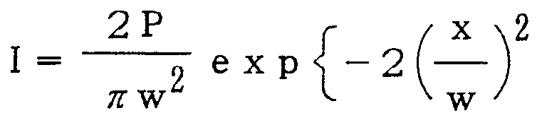
さ ら に 、 こ の拡が り 角 自 体の値の大 き さ の た め、 必然 的 に こ れを コ リ メ 一 卜 す る コ リ メ ー タ レ ン ズの焦点距離 は数 m m前後 と 小 さ く な る 。 半導体 レ ー ザ一 ア レ イ と コ リ メ 一 夕 レ ン ズの距離が僮かで (例え ば数十 m ) も 変 動す る と 、 得 ら れ る コ リ メ 一 ト 光 (平行 ビ ー ム ) が平行 で は な く な り 、 結像光学系への入射時の ビー ム 径 も 変動 し 、 像担持体上での結像ス ポ ッ 卜 サ イ ズが変化 し て し ま う 。 従 っ て半導体 レ ー ザー と コ リ メ 一 夕 レ ン ズの調整許 容範囲が非常に小 さ く な り 、 生産性が悪い と い う 問題点 があ っ た。 ま た 、 初期的 に は正確に調整 し て あ っ て も 、 使用 時の光学系周辺の温度上昇や経年に よ る 部材の変形 の た め コ リ メ 一 夕 レ ン ズの位置が狂 い 、 や は り 、 結像 ス ポ ッ ト 径が変動 し て し ま い、 画像品質が劣化す る と い う 問題があ っ た。 Furthermore, due to the large value of the divergence angle itself, the focal length of the collimator lens that inevitably collimates this is around several mm. And it becomes small. If the distance between the semiconductor laser array and the collimator lens varies with the distance (for example, several tens of meters), the collimated light (parallel beam) ) Will not be parallel, the beam diameter at the time of incidence on the imaging optical system will also fluctuate, and the size of the imaging spot on the image carrier will change. . As a result, the allowable range of adjustment of the semiconductor laser and the collimation lens became very small, and there was a problem that productivity was poor. Also, even if the initial adjustment is accurate, the position of the lens is incorrect due to the temperature rise around the optical system during use and the deformation of members due to aging. However, there was a problem that the imaging spot diameter fluctuated and the image quality deteriorated.
さ ら に 、 複数の平行な光軸を持つ レ ー ザ一 ビー ム 力く こ の コ リ メ ー タ レ ン ズに入射す る と 、 そ の光軸 は大 き な 角 度を も っ て ひ ろ 力く つ て い つ て し ま う 。 い ま 簡単の た め に 、 レ ー.ザ一 ビー ム の数力《 2 本で、 コ リ メ 一 夕 レ ン ズ、 結像 レ ン ズがいずれ も 凸の単 レ ン ズであ る レ ー ザ走査光学系
一 1 s — を考え る 。 図 8 は こ の光学系の光路上の断面図を示 し た も ので、 半導体 レ ー ザ一 ア レ イ 1 を間隔 d で射出 し た 2 本の レ ー ザー ビー ム は、 焦点距離 f c の コ リ メ ー タ レ ン ズ 2 で平行に な る 。 こ こ で半導体 レ ー ザー ア レ イ 1 は コ リ メ ー タ レ ン ズ 2 の物体側焦点におかれてい る ので、 2 本の レ ー ザ一 ビー ム は像側焦点 F で交差す る 。 こ の ほぼ 平行な 2 本の レ ー ザー ビー ム を像面 1 1 に锆像 さ せ る た め、 焦点距離 f i の結像 レ ン ズ 4 をそ の物体側焦点が前 記の コ リ メ ー タ レ ン ズ 2 の像側焦点 F に一致す る よ う に 置 く 。 な お 、 偏 向 装置 の 鏡面 は光学的 に はパ ワ ー を持 た な い の で こ こ で は 省略 し て あ る 。 例え ば像面 1 1 で 1 0 0 m ( こ こ で ス ポ ッ ト 径、 ビ ー ム径は、 ビー ム の 断面の 強度分布がガウ ス分布と し て、 ピー ク 強度に対 し て I Z e 2 のパ ワ ー と な る 直径 と 定義す る ) の ス ポ ッ 卜 6 に結像 さ せ る 場合、 f i を 2 0 0 m m と すれば結像 レ ン ズへの入射 ビー ム径 (すな わ ち コ リ メ ー ト 径) W c は 約 2 m m であ る 。 こ の ビー ム 径を得 る た め に は、 コ リ メ 一 夕 レ ン ズ 2 の焦点距離 f c は約 3 m m と な る 。 図 8 で 明 ら 力、 な よ う に 像面で の ス ポ ッ ト の 間隔 d ' は f c と f i の比に d を掛け た も のであ る 。 現在の半導体 レ ー ザ 一ア レ イ では、 お互い の干渉を避け る た め、 そ の発光部 の 間隔 は 1 0 0 m以下にす る の は難 し い。 従 っ て、 今 の例では、 像面上での ス ポ ッ ト 間隔 d ' は、
一 一 f i 200 Further, when a laser beam having a plurality of parallel optical axes is incident on the collimator lens, the optical axis has a large angle. Let's do it very hard. For the sake of simplicity, let's say that the laser beam has a power of <2 and the collimation lens and the imaging lens are both convex single lenses.ー Laser scanning optical system Consider one 1 s —. Fig. 8 shows a cross-sectional view of the optical system on the optical path.The two laser beams emitted from the semiconductor laser array 1 at an interval d have a focal length of fc. Become parallel at collimator lens 2. Here, since the semiconductor laser array 1 is located at the object-side focal point of the collimator lens 2, the two laser beams intersect at the image-side focal point F. . In order to form the two nearly parallel laser beams on the image plane 11, the imaging lens 4 with the focal length fi is set so that its object-side focal point is the collimation described above. Position the lens so that it coincides with the image-side focal point F of lens 2. The mirror surface of the deflecting device is omitted here because it has no optical power. For example, 100 m at the image plane 11 (where the spot diameter and beam diameter are defined as the Gaussian distribution of the intensity distribution of the beam cross section and the IZ with respect to the peak intensity. If the path follower over the ing diameter of e 2 Ru is imaged on the scan pop Bok 6 to that) definition, the incident beam diameter of fi to a 2 0 0 mm and them if imaging les emission's ( That is, the collimation diameter) Wc is about 2 mm. In order to obtain this beam diameter, the focal length fc of the lens 2 is about 3 mm. In Fig. 8, the apparent distance between the spots d 'on the image plane is the ratio of fc to fi multiplied by d. In today's semiconductor laser arrays, it is difficult to keep the spacing between the light-emitting parts to less than 100 m in order to avoid mutual interference. Therefore, in the present example, the spot interval d 'on the image plane is One one fi 200
d' = x d x 0. 1=6. 6 (mm) CI) d '= x d x 0.1 = 6.6 (mm) CI)
f c 3 f c 3
と な っ て し ま う 。 ま た 、 回転多面鏡の各小面の倒れ角 度の差を補正す る い わ ゆ る 倒れ補正光学系を有す る 場合、 各 レ ン ズ と コ リ メ 一 夕 レ ン ズ と の相対距離に よ っ て、 各 レ ー ザー ビ ー ム の光軸がな す角 度 は さ ら に大 き く な っ て し ま う こ と 力《あ る 。 そ の た め さ ら に レ ン ズを追加 し た り 、 例え ば特開昭 It will be. When a so-called tilt correction optical system that corrects the difference between the tilt angles of the facets of the rotary polygon mirror is provided, the relative distance between each lens and the collimation lens Depending on the distance, the angle formed by the optical axis of each laser beam can be even greater. For this purpose, additional lenses have been added or
5 8 — 2 1 1 7 3 5 に示 さ れ る よ う に 、 プ リ ズム を入れ る な ど し て レ ー ザー ビー ム の光軸の相互の角度の補正を 行な う 構造が提案 さ れて い た。 し か し こ れ ら の構造 は、 光学系の構成を よ り 複雑 に し 、 高価で調整 も 難 し く な る £ な お、 図 8 に お い て は、 簡単の た め倒れ補正 レ ン ズ は省 略 し て あ る 。 As shown in 5 8 — 2 1 1 7 3 5, a structure has been proposed that corrects the mutual angle of the laser beam optical axis by inserting a prism. Had been. Teeth or to come are these structures, the complexity Ri by the configuration of the optical system, the adjustment in expensive that Do rather than flame-£ tail, is have you in Figure 8, because simple was of fallen correction-les-down Are omitted.
次に、 図 9 に従来の像担持体上での走査線 に対す る ス ポ ッ ト 位置の関係を し めす。 こ の例で は ス ポ ッ ト は 4 力、 所、 すな わ ち 4 本の レ ー ザ一 ビ ー ム で書込み を行な っ て い る 。 上記に述べた よ う に、 レ ー ザー 走査光学系で は拡 大光学系 と な り 、 半導体 レ ー ザ一 ア レ イ 上で の ス ポ ッ ト 間隔 は像担持体上で は図中 の d ' の よ う に拡大 さ れ、 通 常、 走査線 9 の 隔 P よ り かな り 大 き く な る 。 例え ば解 像度 3 0 0 d p i ( dot par i nch、 1 イ ン チ Next, FIG. 9 shows a relationship of a spot position with respect to a scanning line on a conventional image carrier. In this example, the spot is writing in four positions, that is, four laser beams. As described above, the laser scanning optical system is a magnifying optical system, and the spot interval on the semiconductor laser array is as shown in the figure on the image carrier. It is enlarged like d ′, and is usually much larger than the interval P of the scanning line 9. For example, resolution 3 0 0 d p i (dot par i nch, 1 inch
[ = 2 5 . 4 m m ] 当 り の ド ッ ト 数) の場合、 P = [= 25.4 mm] number of dots), P =
2 5 . 4 / 3 0 0 = 8 4 . 7 m であ る 力く、 ス ポ ッ ト 間
隔 は前記の よ う に 6 . 7 m m と い う 値に な っ て し ま う 。 そ の た め ス ポ ッ 卜 6 の中心を結ん だ線 1 2 と 走査線 9 の なす角度 α は、 こ の場合では、 25.4 / 300 = 84.7 m Powerful, sport-to-sport The distance will be 6.7 mm, as mentioned above. Therefore, the angle α between the line 12 connecting the center of the spot 6 and the scanning line 9 is, in this case,
Ρ Ρ
= s i n 1 = 0. 7 2 (度) ( 2) d ' と 非常に小 さ な も の と な る 。 半導体 レ ー ザー ア レ イ 1 上 での発光部を結ん だ線 (すな わ ち接台面の端面) も走査 面に対 し て な だけ傾けて取 り 付け る必要があ り 、 α が小 さ く な る に従い、 極めて微妙な調整が必要であ っ た。 = s i n 1 = 0.72 (degrees) (2) d 'is very small. The line connecting the light-emitting parts on the semiconductor laser array 1 (that is, the end face of the mounting surface) must also be mounted at an angle with respect to the scanning surface, and α is small. As they got smaller, very subtle adjustments were needed.
ま た、 一般に半導体 レ ー ザ一 か ら 射出 さ れ る レ ー ザ一 ビー ム の偏光は直線偏光であ り 、 レ ー ザー ビー ム の偏光 面の方向 は半導体 レ ー ザー ァ レ イ の接合面の傾 き に よ つ て一意に き ま っ て し ま う 。 と こ ろ が一般に反射面での反 射率はそ の鏡面への入射角度に よ っ て Ρ 偏光 と S 偏光に よ っ て反射率が異な る 。 図 1 0 に金属 ミ ラ ー の Ρ 偏光、 S 偏光の各々 の反射率 R p 、 R s を示す。 回転多面鏡の 回転に伴 い そ の鏡面への入射角が変化す る ので、 図 1 0 に 示すよ う に P 偏光 と S 偏光の合成 と し て表わ さ れ る レ — ザ一 ビ ー ム の光量 も変動 し て し ま う 。 特に回転多面鏡 で の偏向角 を大 き く と る場合 に 問題 と な る 。 こ れを避け る た め特開昭 5 8 — 4 2 0 2 5 に示すよ う に偏光面を回 転多面鏡の 回転軸 に対 し て 4 5 ° 傾け る 方法 も 提案 さ れ てい る が、 前述の よ う に、 端面発光型の半導体 レ ー ザー ア レ イ 1 で は走査線間隔の制約か ら 、 こ の傾 き 角度が決
一 2 ま っ て し ま う た め、 こ の方法を用 い る こ と はで き な い。 こ の 場 合 は 、 1 / 4 λ 板等を用 い て偏光面を回転 さ せ な く て はな ら な い 、 と い う 問題点力くあ っ た。 Generally, the laser beam emitted from the semiconductor laser beam is linearly polarized light, and the direction of the polarization plane of the laser beam is the junction of the semiconductor laser array. It is uniquely determined by the inclination of the surface. However, in general, the reflectivity at the reflecting surface differs depending on the angle of incidence on the mirror surface, and the reflectivity differs depending on the と -polarized light and the S-polarized light. Figure 10 shows the reflectances R p and R s of Ρ-polarized light and S-polarized light of a metal mirror. Since the angle of incidence on the mirror surface changes with the rotation of the rotating polygon mirror, the laser beam expressed as a combination of P-polarized light and S-polarized light as shown in Fig. 10 The amount of light in the system also fluctuates. This is a problem particularly when the deflection angle of the rotating polygon mirror is increased. In order to avoid this, a method has been proposed in which the polarization plane is inclined by 45 ° with respect to the rotation axis of the rotating polygon mirror as disclosed in Japanese Patent Application Laid-Open No. 58-42025. As described above, in the edge-emitting type semiconductor laser array 1, the tilt angle is determined by the restriction of the scanning line interval. I can't use this method because I'm sorry. In this case, the problem was that the plane of polarization had to be rotated using a 1/4 λ plate or the like.
さ ら に 、 半導体 レ ー ザー ア レ イ 1 を射出 し た 各 レ ー ザ 一 ビ ー ム は 同一の コ リ メ 一 夕 レ ン ズ 2 に入射す る 。 こ の と き 、 図 8 に示す よ う に各 レ ー ザー ビー ム の コ リ メ 一 ト 径 W c は レ ー ザ― ビ ー ム の拡カ《 り 角 Θ と 半導体 レ ー ザー ア レ イ 1 力、 ら コ リ メ 一 夕 レ ン ズ 2 ま で の距離 f c で決 ま る 力 、 レ ン ズま での距離 は各 レ ー ザ一 ビー ム と も 同一で あ る の で、 レ 一 ザ一 ビ ー ム の拡が り 角 0 の み で決 ま る 。 と こ ろ が従来の端面発光型半導体 レ ー ザー ア レ イ 1 で は こ の 拡が り 角 は各発光部毎 に ば ら つ く た め、 各 レ ー ザー ビ ー ム の コ リ メ 一 ト 径 W c も ば ら つ き を も つ。 従 っ て、 こ の コ リ メ ー ト さ れた レ ー ザ一 ビー ム を結像 さ せた ス ポ ッ ト サイ ズ も ば ら つ い て し ま う 。 通常 ご く 普通 に使用 さ れて い る レ ー ザ一 ビ ー ム を 1 本 し か用 い な い ( シ ン グル ビ ー ム の ) レ 一 ザ一走査光学系で は図 1 1 に示すよ う に コ リ メ 一 タ レ ン ズ 2 の前後 ど ち ら 力、 に絞 り 1 3 を いれて コ リ メ 一 卜 径 W c を調整す る よ う な ビ ー ム整形を行な う こ と 力く出来 る が、 図 8 の よ う に複数の レ ー ザ一 ビー ム が 重な っ て入射す る 場台 に は絞 り を コ リ メ 一 タ レ ン ズの焦 点位置 に し かお く こ と はで き な い。 Further, each laser beam emitted from the semiconductor laser array 1 is incident on the same collimator lens 2. At this time, as shown in FIG. 8, the collimation diameter Wc of each laser beam is equal to the expansion angle of the laser beam and the semiconductor laser array. Since the distance between the force and the lens, which is determined by the distance fc to the lens 2 and the lens 2, is the same for each laser beam, The spread angle of the beam is determined only by the angle of 0. However, in the conventional edge-emitting type semiconductor laser array 1, the divergence angle varies for each light-emitting section, so that the laser beam collimated. The diameter Wc also varies. Therefore, the spot size which imaged this collimated laser beam also varies. Fig. 11 shows a single-beam (single-beam) laser-scanning optical system that uses only one laser beam that is normally used. In this way, perform beam shaping such as adjusting the collimator diameter Wc by putting a throttle 13 on either side of the collimator lens 2 before or after the collimator lens 2. As shown in Fig. 8, the aperture should be set at the focal point of the collimator lens on the stage where multiple laser beams are incident upon each other as shown in Fig. 8. I can't do that.
一般に半導体 レ ー ザ 一 ア レ イ に お い て は 、 レ ー ザ 一 発 拫 は光共振器を流れ る 電流が一定値を超え な ければ生 じ
― つつ 一 な い。 こ の電流値を 「 し き い値電流」 と 呼ぶが、 従来の 半導体 レ ー ザー ア レ イ では 「 し き い値電流」 が数 1 0 m A も あ り 、 そ の熱に よ っ て レ ー ザー ビー ム の特性、 特 に発振波長の シ フ ト が生ず る た め、 半導体 レ ー ザー ァ レ ィ か ら の放熱が問題 と な っ てい た。 特に、 複数の ビー ム を射出する 半導体 レ ー ザー ア レ イ では、 発光部の数だけ 熱源があ り 、 多数の発光部を集積す る 際の障害 と な っ て い た。 Generally, in a semiconductor laser array, a laser beam is generated if the current flowing through the optical resonator does not exceed a certain value. -There is no one. This current value is called the “threshold current”. In a conventional semiconductor laser array, the “threshold current” is as high as several 10 mA, and it depends on the heat. Due to the characteristics of the laser beam, especially the shift of the oscillation wavelength, heat radiation from the semiconductor laser array has been a problem. In particular, in a semiconductor laser array that emits a plurality of beams, the number of heat sources is equal to the number of light emitting parts, which has been an obstacle to integrating a large number of light emitting parts.
1 — 2 本発明 の構成 1 — 2 Configuration of the present invention
本発明の一実施例を以下に説明す る 。 図 2 は本発明の 画像形成装置の全体を示す図であ る。 転写材 5 1 上に 印 刷結果を得 る プ ロ セ ス は い わ ゆ る 電子写真プ ロ セ ス に よ つ て い る 。 像担持体 5 と し て は、 半導体 レ ー ザー を光源 に用 い た電子写真プ リ ン タ では長波長側に增感 し た有機 感光体 ( O P C ) が多 く 用 い ら れ る 。 こ の像担持体 5 は ま ず、 蒂電器 5 2 で一定の表面電位に帯電 さ れた の ち 、 レ ー ザー ビー ム走査装置 5 3 に よ っ て光書込すな わ ち露 光が行なわれ る 。 こ の レ ー ザー ビー ム走査装置 5 3 力、 ら 画像情報に従 っ て光強度が各々 独立に変調 さ れた複数の レ ー ザー ビー ム 5 4 が像担持体 5 を軸方向 に走査 し 、 露 光部の み に表而電位を打ち 消す電荷を発生 さ せ、 そ の部 分の表面電位の絶対値は小 さ く な る 。 結果 と し て像担持 体 5 上に は画像 に応 じ た表面電位の分布、 すな わ ち静電 潜像が形成 さ れる 。 静電潜像 は現像器 5 5 に よ っ て表面
電位に応 じ て選択的 に現像剤を付着 さ せ る こ と に よ り 現 像 さ れ る 。 こ の現像剤は転写器 5 6 に よ っ て転写材 5 1 (通常は紙) に転写 さ れ る 。 転写材 5 1 上の現像剤 は、 定着器 5 7 に よ っ て熱圧力定着 さ れ排出 さ れ る 。 One embodiment of the present invention will be described below. FIG. 2 is a diagram showing the entire image forming apparatus of the present invention. The process for obtaining the printing result on the transfer material 51 is based on the so-called electrophotographic process. As the image carrier 5, in an electrophotographic printer using a semiconductor laser as a light source, an organic photoreceptor (OPC) sensitive to the long wavelength side is often used. First, the image carrier 5 is charged to a constant surface potential by a dynasty device 52, and then optically written by a laser beam scanning device 53, that is, light is exposed. It is done. The laser beam scanning device 53 has a plurality of laser beams 54 whose light intensity is independently modulated according to the image information, and scans the image carrier 5 in the axial direction. However, a charge is generated only in the exposed portion, which cancels the meta-potential, and the absolute value of the surface potential in that portion is reduced. As a result, a distribution of the surface potential according to the image, that is, an electrostatic latent image is formed on the image carrier 5. The electrostatic latent image is developed by the developing unit 55 The image is formed by selectively applying the developer according to the potential. This developer is transferred to a transfer material 51 (usually paper) by a transfer device 56. The developer on the transfer material 51 is fixed by heat and pressure by a fixing device 57 and discharged.
図 1 は本発明 の画像形成装置 に用 い る レ ー ザ ー ビ ー ム 走査装置 5 3 の概観図であ る 。 図 2 に示 し た レ ー ザー ビ ー ム走査装置 5 3 で は レ ー ザー ビ ー ム 5 4 は折 り 曲 げ ら れて下方 に射出す る 場合を想定 し て い た が、 こ こ で は説 明 の た め単純化 し て描い てあ る 。 FIG. 1 is a schematic view of a laser beam scanning device 53 used in the image forming apparatus of the present invention. In the laser beam scanning device 53 shown in FIG. 2, it is assumed that the laser beam 54 is bent and emitted downward. Is simplified for illustration.
図 1 に お い て、 半導体 レ ー ザー ア レ イ 2 1 は複数の発 光部 2 1 a が 2 次元状 に素子基板 2 2 (図 3 ) 上 に配置 さ れてお り 、 コ リ メ ー タ レ ン ズ 2 に よ っ て所定の ビー ム 直径を持つ レ ー ザー ビー ム に コ リ メ ー ト (平行化) さ れ る 。 発光部 2 1 a は制御装置 6 0 に よ っ て個別 に そ の点 灯お よ び光量が制御 さ れ る 。 こ の レ ー ザー ビー ム は回転 多面鏡 3 の 1 つ の小面に入射 し 、 そ の 回転 に伴 っ て、 各 々 偏向 さ れ る 。 結像 レ ン ズ 4 を通過 し た レ ー ザ一 ビー ム は像担持体 5 上で ス ポ ッ ト 6 に結像す る 。 図 1 に お い て、 倒れ補正 レ ン ズは簡単の た め省略 し て あ る 。 In FIG. 1, a semiconductor laser array 21 has a plurality of light emitting portions 21a arranged two-dimensionally on an element substrate 22 (FIG. 3). The laser lens 2 is collimated (parallelized) to a laser beam having a predetermined beam diameter. The light emitting section 21a is individually controlled by the control device 60 so that the light is turned on and the light amount is controlled. The laser beam is incident on one of the small faces of the rotating polygon mirror 3 and is deflected by the rotation. The laser beam that has passed through the imaging lens 4 forms an image on the spot 6 on the image carrier 5. In FIG. 1, the tilt correction lens is omitted for simplicity.
こ の様な特性を持つ半導体 レ ー ザー ァ レ イ 2 1 と し て は、 いわ ゆ る 面発光型半導体 レ ー ザ ー ア レ イ を用 い る の が好 ま し い。 さ ら に よ り 望ま し く は、 Π — VI族化合物半 導体を埋め込ん だ発光部を有す る 面発光半導体 レ ー ザー ア レ イ が用 い ら れ る 。 図 3 は こ の面発光型半導体 レ ー ザ
一ア レ イ 2 1 の発光部 2 1 a の う ち の 1 つ の断面図であ る 。 図 3 に おいて、 1 つ の光共振器が素子基板 2 2 上に 2 次元的 に配置 さ れた 1 つ の発光部 に対応 し てい る 。 As the semiconductor laser array 21 having such characteristics, it is preferable to use a so-called surface-emitting type semiconductor laser array. More desirably, a surface-emitting semiconductor laser array having a light-emitting portion in which a III-VI compound semiconductor is embedded is used. Figure 3 shows this surface-emitting type semiconductor laser. FIG. 3 is a cross-sectional view of one of the light emitting portions 21a of the array 21. In FIG. 3, one optical resonator corresponds to one light-emitting portion arranged two-dimensionally on the element substrate 22.
図 3 に おいて G a A s 基板 2 2 の上に、 組成の違 う 2 種の A 1 G a A s 層を数 1 0 層積層 し た半導体多層膜反 射層 2 3 が形成 さ れ、 そ の上に それぞれ A 1 G a A s 力、 ら な る ク ラ ッ ド層 2 4 、 活性層 2 5 、 ク ラ ッ ド層 2 6 、 コ ン タ ク ト 層 2 7 が積層 さ れ、 最後 に S i 0 2 誘電体多 層膜反射層 2 8 が形成 さ れてい る 。 ま た G a A s 基板 2 2 の裏面全体及び、 表面の誘電体多層反射層の ま わ り に窓状の電極 2 9 、 3 0 が形成 さ れてお り 全体が光共振 器を構成 し てい る。 In FIG. 3, on a GaAs substrate 22, a semiconductor multilayer reflection layer 23 formed by stacking several 10 types of A 1 GaAs layers having different compositions is formed. A1 GaAs layer, an active layer 24, an active layer 25, a layer 26, and a contact layer 27 are laminated on each other. Finally, a SiO 2 dielectric multilayer reflection layer 28 is formed. Further, window-like electrodes 29 and 30 are formed on the entire back surface of the GaAs substrate 22 and around the dielectric multilayer reflective layer on the front surface, and the whole constitutes an optical resonator. ing.
活性層 2 5 で発生 し た光は基板 2 2 面 と垂直方向 に、 上下の反射層 2 7 、 2 3 の間を往復 し発振す る ので、 そ の レ ー ザ一 ビー ム 3 1 の光軸 は基扳 2 2 面に対 し てほぼ 垂直 と な る。 光共振器の回 り に は埋め込み層 3 2 と し て Π - VI族の 化合物半導体が埋め込ま れてい る 。 Π — VI族 の 化 ^物半導体 と し て は、 Π 族元素 と し て Z n 、 C d 、 H g 、 VI族元素 と し て 0、 S 、 S e 、 T e を 2 〜 4 元素 組み 台わせ、 ま た、 そ の化合物の格子定数を前記の ク ラ ッ ド層 2 4 、 活性 ¾ 2 5 、 ク ラ ッ ド層 2 6 力、 ら な る 半導 体層の格子定数に合わせ る の が望ま し い。 こ の Π — VI族 の 化 ^物半導体は ^気抵抗が非常に大 き い た め、 電流を 光共振器の なかに効率的 に 閉 じ こ め る 。 ま た 、 埋め込み
層 3 2 は光共振器を構成 し て い る A 1 G a A s 半導体層 と は屈折率に差があ る た め、 光共振器の 内部で素子基板 2 2 面 に垂直 も し く はそ れに近い角度で進む光は こ の埋 め込み層 3 2 と の界面で全反射 し 効率的 に 閉 じ こ め ら れ o The light generated in the active layer 25 reciprocates between the upper and lower reflective layers 27 and 23 in the direction perpendicular to the surface of the substrate 22 and oscillates, so that the light of the laser beam 31 is generated. The axis is almost perpendicular to the base 22 surface. A group III-VI compound semiconductor is buried around the optical resonator as a buried layer 32. Π — Group VI compound semiconductors include Zn, Cd, and Hg as Group IV elements and 0, S, Se, and Te as Group VI elements in groups of 2 to 4 elements. The lattice constant of the compound is adjusted to the lattice constants of the above-mentioned cladding layer 24, active layer 25, cladding layer 26, and the resulting semiconductor layer Is desirable. This Π—VI compound semiconductor has a very high air resistance, so that current can be efficiently confined in the optical resonator. Also, embedding Since the layer 32 has a difference in the refractive index from the A 1 GaAs semiconductor layer constituting the optical resonator, the layer 32 is perpendicular to the surface of the element substrate 22 inside the optical resonator. Light traveling at an angle close to that angle is totally reflected at the interface with the buried layer 32, and is efficiently closed.
こ の た め 、 こ の よ う な半導体 レ ー ザ一 ア レ イ 2 1 を用 いれば、 従来の半導体 レ ー ザ一 ァ レ イ に比べて大変小 さ い電流で レ ー ザー発振が始 ま る 。 すな わ ち 、 し き い値電 流が低い。 よ っ て、 複数の発光部 2 1 a をア レ イ 化 し て 1 つ の素子基板 2 2 上に集積 し て も 、 素子基板 2 2 で の 損失熱量が少な く よ り 多 く の光パ ワ ー も し く は発光部 2 1 a の数を得 る こ と 力く出来 る 。 Therefore, if such a semiconductor laser array 21 is used, laser oscillation starts with a very small current as compared with a conventional semiconductor laser array. I will. That is, the threshold current is low. Therefore, even if the plurality of light emitting portions 21a are arrayed and integrated on one element substrate 22, the amount of heat loss in the element substrate 22 is small and more light paths are provided. It is possible to obtain the number of wires or light emitting portions 21a.
ま た 、 面発光半導体 レ ー ザー ア レ イ 2 1 は、 レ ー ザ一 ビ ー ム の射出部 (発光部) 2 1 a の断面積 (ニ ァ ♦ フ ィ — ノレ ド · パ タ ー ン ) が、 従来の端面発光型の半導体 レ ー ザ一 に比べて比較的大 き く と れ る た め、 レ ー ザー ビ ー ム の拡カ《 り 角 は小 さ く な る 。 こ の拡カく り 角 の大 き さ は射出 窓の面積で決ま る が、 そ の面嵇 はエ ッ チ ン グ等で正確に 制御で き る た め、 拡カ り 角 も 一定にす る こ と 力《で き る 。 さ ら に 、 レ ー ザ一 ビー ム の拡カ り 角 の縦横すな わ ち楕円 断面 ビ ー ム の長径 と 短 ii の比 も こ の射出窓の形状で随意 に設定で き る 。 例え ば、 全な 円形窓 にすれば、 等方的 な拡カ《 り 角 を持つ 円 形断 20の レ ー ザー ビー ム が得 ら れ る £ 従 っ て、 光 $ώ方向 の断面 に よ る ビー ム の非点隔差 も 少な
と こ ろ が、 通常の レ ー ザ一 ビー ム プ リ ン タ 一 では、 像 担持体上での レ ー ザー ビー ム の結像ス ポ ッ 卜 の形状 は走 査方向 に短軸が一致す る よ う な楕円状 と す る 事が多 い。 こ れは、 走査方向 に は点灯時間だけ ス ポ ッ ト が移動 し像 が長 く 伸 びる ので、 こ れを補正す る た めであ る 。 そ の た め に は結像光学系に入射する レ ー ザー ビー ム の断面形状 は、 逆に走査方向 に長軸を も つ楕円であ る こ と が望ま し い。 上記で述べた よ う に、 面発光の半導体 レ ー ザー ァ レ ィ 2 1 で は射出 ビー ム の楕円比を 自 由 に制御で き る の で、 特別な光学系を用 い な く と も 、 走査面に長軸を有 し 、 適 切な長軸 と短軸の比を持つ よ う な断面を も つ レ ー ザー ビ 一ム を結像光学系に入射 さ せ る こ と がで き る 。 The surface-emitting semiconductor laser array 21 has a cross-sectional area of a laser beam emitting portion (light-emitting portion) 21a (near ♦ field pattern). ) Is relatively large compared to conventional edge-emitting semiconductor lasers, so that the divergence angle of the laser beam is small. The size of this divergence angle is determined by the area of the exit window, but the divergence angle must be kept constant because the area can be controlled accurately by etching or the like. I can do it. Furthermore, the ratio of the divergence angle of the laser beam, ie, the ratio of the major axis to the minor axis ii of the elliptical cross-section beam, can be arbitrarily set by the shape of the injection window. For example, if the entire circular window, Les over Heather beam of the circle Katachidan 20 with an isotropic拡Ka "Ri corners Ru is obtained, et al. £ and follow, in light $ ώ direction of the cross section The beam has a small astigmatic difference However, in a normal laser beam printer, the shape of the imaging spot of the laser beam on the image carrier has the minor axis coincident with the scanning direction. It is often shaped like an ellipse. This is because the spot moves in the scanning direction for the lighting time and the image is elongated, so that this is corrected. To that end, it is desirable that the cross-sectional shape of the laser beam incident on the imaging optical system be an ellipse having a major axis in the scanning direction. As described above, in the surface-emitting semiconductor laser array 21, since the ellipticity of the emission beam can be controlled freely, it is not necessary to use a special optical system. A laser beam having a major axis in the scanning plane and a section having an appropriate ratio of the major axis to the minor axis can be incident on the imaging optical system. .
ま た、 こ の面発光半導体 レ ー ザ一 ア レ イ 2 1 は上述の よ う に 各発光部 2 1 a 力、 ら の レ ー ザー ビー ム の拡カ《 り 角 を均一にで き る 。 よ っ て、 コ リ メ ー タ レ ン ズ も し く は結 像光学系への入射 ビー ム径を各 レ ー ザー ビー ム と も ほぼ 一定に管理で き 、 結梁 と し て像担持体上での結像 ス ポ ッ ト サ イ ズ も一定にで き る。 In addition, as described above, the surface emitting semiconductor laser array 21 can make uniform the expansion angle of the laser beam of each light emitting portion 21a as described above. . Thus, the diameter of the collimator lens or the incident beam to the imaging optical system can be controlled almost uniformly for each laser beam, and the image carrier can be used as a beam. The imaging spot size above can also be constant.
面発光半導体 レ ー ザー ア レ イ 2 1 では共振器の素子基 扳 2 2 面内での断面積が大 き く な る と 、 0 次モ ー ドだけ ではな く 、 高次の モ ー ドの発振が始ま り 、 結像 し た ス ポ ッ 卜 の光量分布 も い く つ も の ピー ク を持ち 、 像担持体 5 上 に静 M潜像を作 る の に は甚だ好ま し く な い。 そ こ で、
複数の小 さ な光共振器を近接 し て並べ、 位相 同期 し て発 振 さ せ る こ と に よ り 、 0 次モ ー ドで発振す る 面積の大 き な発光部 2 1 a を得 る こ と が出来 る 。 In the surface-emitting semiconductor laser array 21, if the cross-sectional area in the plane of the resonator element 22 becomes large, not only the 0-order mode but also the higher-order mode Oscillation starts, the light intensity distribution of the formed spot has several peaks, and it is extremely unfavorable to form a static M latent image on the image carrier 5. . Therefore, By arranging a plurality of small optical resonators close to each other and oscillating them in phase synchronization, a light emitting unit 21a with a large area that oscillates in the 0th-order mode is obtained. Rukoto can .
こ の位相同期型面発光半導体 レ ー ザー ァ レ イ 2 1 の 1 つ の発光部 2 l a の一部断面図を図 4 に示す。 こ こ で は 複数の光共振器が非常に狭い 間隔で隣接 し てお り 、 埋め 込み層 3 2 の下部 は活性層 2 5 に達 し て い な い。 こ の た め、 埋め込み層 3 2 下方の ク ラ ッ ド層 2 6 を介 し て隣接 す る 光共振器か ら 漏れ る 光が互い に影響 し 、 同位相で発 振す る 。 こ の た め 、 こ の 隣接す る 複数の光共振器があ た か も 1 つ の光共振器の よ う に動作す る 。 こ の よ う に各光 共振器の射出光の波面が揃 う の で、 面状の レ ー ザ一放射 源 と し て作用 し 、 そ の発光部の見か け上の面積 は大 き く な る た め、 レ ー ザー ビー ム の拡カ《 り 角 は非常 に小 さ く 、 半値全角 で 2 度以下 にす る こ と も 可能であ る 。 FIG. 4 shows a partial cross-sectional view of one light-emitting portion 2 la of the phase-locked surface-emitting semiconductor laser array 21. Here, a plurality of optical resonators are adjacent to each other at a very small interval, and the lower part of the buried layer 32 does not reach the active layer 25. For this reason, light leaking from adjacent optical resonators via the cladding layer 26 below the buried layer 32 affects each other and emits in phase. For this reason, the plurality of adjacent optical resonators behave as if they were one optical resonator. Since the wavefronts of the light emitted from the optical resonators are aligned in this way, they act as a planar laser radiation source, and the apparent area of the light-emitting part is large. For this reason, the divergence angle of the laser beam is very small, and it is possible to make the full width at half maximum less than 2 degrees.
こ の よ う に 位相 同期を行な う 面発光半導体 レ ー ザー ァ レ イ 2 1 で は、 レ ー ザー ビー ム の拡カ り 角 が従来の半導 体 レ ー ザー に比べて小 さ く な る が、 こ れを従来の実施例 と 対比 し て説明す る 。 例え ば レ ー ザ一 ビー ム の拡が り 角 を半値全角 で 2 度 と し 、 先の例 と 同 じ く 直径 2 m m の ビ 一ム 径で結像光学系 に 入射 さ せ る と す る と コ リ メ 一 夕 レ ン ズ の焦点距離 f c は約 3 5 m m に な る 。 こ の よ う に コ リ メ タ レ ン ズ 2 の焦点距離 f c を長 く す る こ と がで き る ので、 半導体 レ ー ザ一 ア レ イ 2 1 に対す る コ リ メ 一 夕
レ ン ズ 2 の距離の調整余裕が増加す る 。 ま た、 像担持体 上での レ ー ザー ビー ム の結像 ス ポ ッ 卜 間隔 d ' は、 半導 体 レ ー ザ一 ア レ イ 2 1 を射出す る レ ー ザ一 ビー ム の 間隔 を d と す る と 、 Thus, in the surface emitting semiconductor laser array 21 that performs phase synchronization, the divergence angle of the laser beam is smaller than that of a conventional semiconductor laser. However, this will be described in comparison with the conventional example. For example, assume that the divergence angle of the laser beam is 2 degrees at full width at half maximum, and the beam is incident on the imaging optical system with a beam diameter of 2 mm as in the previous example. The focal length fc of the lens will be about 35 mm. Since the focal length fc of the collimator lens 2 can be lengthened in this way, the collimation of the semiconductor laser array 21 can be shortened. The margin for adjusting the distance of the lens 2 is increased. Further, the imaging spot interval d 'of the laser beam on the image carrier is the interval between the laser beam emitted from the semiconductor laser array 21. If d is
f i 200 f i 200
x d xO. 1=0. 57 (mm) (3) f c 35 x d xO. 1 = 0.57 (mm) (3) f c 35
と な り 、 走査線間隔 も従来例 と 同 じ 8 4 . 7 ^ m と す る と 、 走査面に対す る ス ポ ッ ト を結ん だ線の角度 α は Assuming that the scanning line spacing is 84.7 ^ m, which is the same as the conventional example, the angle α of the line connecting the spot to the scanning surface is
Ρ Ρ
-1 -1
な = s η 8. 55 渡) (4) Na = s η 8.55 pass) (4)
d' d '
と な り 、 従来の半導体 レ ー ザー ア レ イ を使 っ た場合 に比 ベて は る かに大 き く 取れ る ( ( 3 ) 式参照) 。 こ の た め、 半導体 レ ー ザー ア レ イ 2 1 の光軸方向回 り の取付調整 も 容易に行な う こ とがで き る と と も に 、 各部品の加工公差 に よ っ て は こ の角度 な の調整を行な わずに組み立て る 二 と も で き る。 ま た、 各結像ス ポ ッ ト や そ こ に至 る ま での レ ー ザー ビー ムが互い に接近 し てい る ので、 光学系の有 効径 も 小 さ く てすむ こ と 力《 こ の 図力、 ら も 明 ら かであ る 。 As a result, it is much larger than when a conventional semiconductor laser array is used (see equation (3)). For this reason, the mounting adjustment of the semiconductor laser array 21 around the optical axis direction can be easily performed, and depending on the processing tolerance of each part. It is possible to assemble without adjusting this angle. In addition, since the imaging spot and the laser beam up to that point are close to each other, the effective diameter of the optical system can be small. The drawing power of the figure is also clear.
さ ら に レ ー ザー ビー ム の拡カ《 り 角 を極端に小 さ く す る こ と に よ り 、 半導体 レ ー ザー ア レ イ 2 1 か ら 回転多面鏡 3 に至 り さ ら に結像 レ ン ズ 4 に い た る 距離の間 に、 レ ー ザ一 ビー ム の大 き さ はあ ま り 広力《 らず、 結像 レ ン ズ 4 の 入射面において も 、 所要の結像 ス ポ ッ ト 径を得 る の に十 分な 小 さ さ にで き る 。 すなわ ち 、 通常の レ ー ザー走查光
学系の よ う な所要の コ リ メ 一 ト 径に レ ー ザ一 ビ ー ム を コ リ メ 一 卜 (平行化) す る コ リ メ ー タ レ ン ズが不要 と な る 但 し 、 回転多面鏡 3 の偏向角 に応 じ て光路長が変 化 し 、 結像 レ ン ズ 4 に入射す る レ ー ザー ビ ー ム の大 き さ も 変化 し て行 く の で、 そ れを補正す る 光学系が必要に な る 。 し 力、 も 、 そ の よ う な光学的機能は結像 レ ン ズ 4 に も たせ る こ と は容易であ る の で、 全体の光学系の構成要素 は少な く 。 Furthermore, the extremely widening angle of the laser beam is reduced so that the connection from the semiconductor laser array 21 to the rotary polygon mirror 3 is further increased. During the distance to image lens 4, the size of the laser beam is not too large, and the required imaging is possible even at the entrance surface of imaging lens 4. It can be small enough to get the spot diameter. That is, normal laser running light The collimator lens for collimating (parallelizing) the laser beam to the required collimation diameter, such as in a academic system, is not required. The optical path length changes in accordance with the deflection angle of the rotating polygon mirror 3, and the size of the laser beam incident on the imaging lens 4 also changes. An optical system for correction is required. Since it is easy to provide such an optical function to the imaging lens 4, there are few components of the entire optical system.
ま た 、 面発光形の半導体 レ ー ザー ア レ イ 2 1 に お い て は、 発光部 2 1 a が互い に干渉 し な い距離 さ え お け ば、 ど こ に で も 発光部 2 1 a を置 く こ と が可能な た め、 素子 基板 2 2 上に 2 次元状 に発光部 2 1 a を配列で き る 。 い ま 、 先 に 図 8 で示 し た従来の実施例 と 同様に 4 本の レ 一 ザ一 ビ ー ム で走査を行な う 露光系を考え る 。 図 5 ( a ) で示す よ う に 4 本の レ ー ザー ビー ム を配列す る と 、 図 5 ( b ) の よ う に一直線 に並べ る 場合 に比べて レ ー ザー ビ ー ム相互の角度 も し く は距離を小 さ く で き 、 光学系の大 き さ を そ れに あ わせて小 さ く で き る 。 Also, in the surface-emitting type semiconductor laser array 21, the light-emitting section 21 can be placed anywhere as long as the light-emitting sections 21 a do not interfere with each other. Since a can be placed, the light emitting portions 21 a can be arranged two-dimensionally on the element substrate 22. Now, let us consider an exposure system that performs scanning with four laser beams in the same manner as the conventional embodiment shown in FIG. When four laser beams are arranged as shown in Fig. 5 (a), the angle between the laser beams is larger than when they are aligned in a straight line as shown in Fig. 5 (b). Alternatively, the distance can be reduced, and the size of the optical system can be reduced accordingly.
上記の例 は レ ー ザー ビー ム が 4 本の場合を示 し た が、 レ ー ザ一 ビー ム の数が更 に増え た場合、 像担持体 5 上で の ス ポ ッ 卜 6 の位置が最 も 近接す る よ う 、 半導体 レ ー ザ — ア レ イ 2 1 上の発光部 2 1 a の配置を 自 由 に選べ る の で、 効果 は よ り 大 き く な る 。 一例 と し て レ ー ザ一 ビ ー ム 数力 8 本の と き の走査線 9 に対す る 結像ス ポ ッ ト 6 の配
置例を図 5 ( c ) に示す。 The above example shows a case where there are four laser beams, but if the number of laser beams further increases, the position of the spot 6 on the image carrier 5 will be changed. Since the arrangement of the light emitting portion 21a on the semiconductor laser-array 21 can be freely selected so as to be closest to each other, the effect is further enhanced. As an example, the arrangement of the imaging spot 6 with respect to the scanning line 9 when the number of laser beams is eight An example is shown in Fig. 5 (c).
な お、 以上の結像 ス ポ ッ 卜 の相対位置の関係は、 必ず し も半導体 レ ー ザー ア レ イ 2 1 上での発光部 2 1 a の配 置 と 相似形では な い。 例え ば、 既に触れた よ う な回転多 面鏡 3 の倒れ捕正光学系等の よ う に、 走査方向 と そ の 直 交方向で光学的特性が異な る光学要素が レ ー ザー ビー ム の途中 に は い っ た場合、 各 レ ー ザー ビー ム相互の なす角 度や距離は、 走査方向 と そ の 直交方向で異な る こ と も あ る。 し か し 、 そ の よ う な場合で も 従来の端面発光半導体 レ ーザー ア レ イ では、 一直線に並ぶ発光部は像担持体上 で一直線上の結像ス ポ ッ ト 列に し かな り 得な い。 こ れに 対 し て本発明 に おいては、 上に述べた よ う な発光部 2 1 a を素子基板 2 2 上に 2 次元的に配列で き る効果は同様 に発揮 さ れる 。 The relationship between the relative positions of the imaging spots described above is not necessarily similar to the arrangement of the light-emitting portion 21a on the semiconductor laser array 21. For example, an optical element having an optical characteristic that differs in the scanning direction and its orthogonal direction, such as the tilting optical system of the rotating polygonal mirror 3 already mentioned, is the same as the laser beam. If you are on the way, the angle or distance between the laser beams may be different between the scanning direction and the direction perpendicular to the scanning direction. However, even in such a case, in the conventional edge emitting semiconductor laser array, the light emitting portions aligned in a line can be formed on the image carrier in a line of imaging spots in a straight line. Absent. On the other hand, in the present invention, the effect of two-dimensionally arranging the light emitting portions 21a on the element substrate 22 as described above is similarly exhibited.
面発光形の半導体 レ ーザー ア レ イ 2 1 におい て も一般 的に、 射出 レ ー ザー ビー ム は直線偏光に な る 。 そ の方向 は共振器の素子基板 2 2 面内の平面形状に よ っ て決ま り 、 おおむね は平面形状の長手方向 に偏光面が一致す る 。 例 え ば楕円状の共振器形状にすればそ の長軸方向が偏光面 に な る 。 前述の よ う に位相同期型の半導体 レ ー ザー ァ レ ィ 2 1 に お い て は 1 つ の発光部は複数例え ば 4 つ の位相 同期 し て発振す る 光共 ^ か ら 構成 さ れてい る 。 こ の と き 射出 レ ー ザー ビー ム の断面形状は各光共振器か ら射出 さ れた レ ー ザー ビー ム の 成 さ れた形状 と な る た め、 個
々 の光共振器の並べ方に よ っ て射出 ビー ム の 断面形状を 自 由 に設定で き る 。 こ の場合 も 偏光面の 向 き は個 々 の共 振器の平面形状で決ま る ので、 例え ば合成 さ れた楕円 の レ ー ザ一 ビー ム を得 る 場合で も そ の長軸 と 偏光面の方向 を独立 に設定で き る 。 In the surface-emitting type semiconductor laser array 21 as well, the emission laser beam is generally linearly polarized. The direction is determined by the plane shape in the plane of the element substrate 22 of the resonator, and the polarization plane generally coincides with the longitudinal direction of the plane shape. For example, if an elliptical resonator shape is used, the major axis direction becomes the polarization plane. As described above, in the semiconductor laser array 21 of the phase-locked type, one light-emitting section is composed of a plurality of, for example, four light beams oscillating in phase synchronization. ing . In this case, the cross-sectional shape of the emission laser beam is the same as the shape of the laser beam emitted from each optical resonator. The cross-sectional shape of the emission beam can be freely set according to the arrangement of the optical resonators. Also in this case, the direction of the polarization plane is determined by the plane shape of each resonator, so even if a synthesized elliptical laser beam is obtained, its long axis and polarization The direction of the surface can be set independently.
図 6 ( a ) は こ の様子を模式的 に示 し た も の で、 半導 体 レ ー ザー ア レ イ 上の 1 つ の発光部 4 2 を ビ ー ム射出側 力、 ら み た平面図であ る 。 図 6 ( a ) に示す よ う に 、 4 つ の位相 同期 し て発振 し て い る 楕円状断面の光共振器 4 1 が 1 つ の発光部 4 2 を構成 し てお り 、 個 々 の光共振器 4 1 力、 ら射出 さ れ る レ ー ザー ビ ー ム の偏光面 4 3 は、 図 6 ( a ) で は 4 5 度傾い てい る が、 合成 し て得 ら れ る 楕 円状の レ ー ザー ビー ム の長軸 は上下方向 に な る 。 ま た 図 6 ( b ) に示す よ う に 、 個 々 の光共振器 4 1 か ら 射出 さ れ る レ ー ザー ビー ム の偏光面 4 3 の方向 を互 い に異な る 角度で配置す る と 、 そ の合成 さ れた射出 レ ー ザ一 ビ ー ム は近似的 に 円偏光 に な る 。 FIG. 6 (a) schematically shows this state.One light emitting section 42 on the semiconductor laser array is viewed from the beam emitting side and viewed from a plane. It is a figure. As shown in FIG. 6 (a), four optical resonators 41 having an elliptical cross section oscillating in phase synchronization form one light emitting section 42, and The polarization plane 43 of the laser beam emitted from the optical resonator 41 is inclined by 45 degrees in FIG. 6 (a), but the elliptical shape obtained by synthesis The long axis of the laser beam is up and down. Also, as shown in FIG. 6 (b), the directions of the polarization planes 43 of the laser beams emitted from the individual optical resonators 41 are arranged at different angles from each other. Then, the synthesized emission laser beam becomes approximately circularly polarized light.
先に も 述べた よ う に通常の レ ー ザ一 ビー ム プ リ ン タ ー で は、 像担持体上での レ ー ザー ビ ー ム の結像ス ポ ッ 卜 6 の 形状 は走査方向 に短軸が一致す る よ う な楕円状 と す る 事が多 い。 そ こ で前述の様 に各光共振器か ら の レ ー ザー ビー ム の 偏光面の 向 き を合成楕円 レ ー ザー ビー ム 断面の 長軸方向 に 対 し て 4 5 度傾 け、 合成 し た射出 ビ ー ム の長 軸を走查方向 に一致 さ せ る よ う に半導体 レ ー ザー ァ レ イ
つ 一 As described above, in a normal laser beam printer, the shape of the laser beam imaging spot 6 on the image carrier is changed in the scanning direction. It is often an ellipse whose minor axes coincide. Therefore, as described above, the direction of the polarization plane of the laser beam from each optical resonator is inclined by 45 degrees with respect to the major axis direction of the cross section of the synthetic elliptical laser beam, and then synthesized. Semiconductor laser array so that the long axis of the injection beam is aligned with the running direction. One
2 1 を設ければ、 各光共振器か ら の レ ー ザー ビー ム の偏 光面は ビー ム走査面と は 4 5 度傾 く こ と に な る 。 そ の結 果、 回転多面鏡 3 の回転軸 に対 し て も偏光面は 4 5 度傾 いてお り 、 図 1 1 に示 し た よ う な 回転多面鏡への入射角 に よ る反射率の差を受け に く い。 こ の こ と は、 ほぼ円偏 光であ る 楕円断面の レ ー ザー ビー ム で も 同様であ る 。 な お、 光学系の構成に よ っ て は、 半導体 レ ー ザー ア レ イ 2 1 力、 ら 射出す る レ ー ザー ビー ム の短軸を走査方向 に一 致 さ せ る 場合 も あ る が、 全 く 同様の効果を発揮す る。 If 21 is provided, the polarization plane of the laser beam from each optical resonator is inclined by 45 degrees with respect to the beam scanning plane. As a result, even with respect to the rotation axis of the rotating polygonal mirror 3, the polarization plane is inclined by 45 degrees, and the reflectance due to the angle of incidence on the rotating polygonal mirror as shown in Fig. 11 Difficult to receive the difference. The same is true for laser beams having an elliptical cross section, which is almost circularly polarized. Note that, depending on the configuration of the optical system, the short axis of the laser beam emitted from the semiconductor laser array 21 may be matched in the scanning direction. It has exactly the same effect.
以上に説明 し た実施例は、 本発明の一実施例 に過 ぎな い。 例え ば偏向装置 と し て回転多面鏡 3 では な く 、 ガル べ ノ ミ ラ 一 やホ ロ グラ ム デ ィ ス ク を用 いて も 同様の効果 を苻す る 。 ま た、 コ リ メ ー タ レ ン ズ、 倒れ補正 レ ン ズ、 結像 レ ン ズの有無、 構成や相対位置関係が変わ っ て も本 発明の効果は同 じ く 発揮 さ れ る 。 The embodiment described above is only one embodiment of the present invention. For example, the same effect can be obtained by using a galvanometer mirror or a hologram disk instead of the rotary polygon mirror 3 as the deflecting device. Further, even if the collimator lens, the tilt correction lens, the presence or absence of the imaging lens, the configuration, and the relative positional relationship are changed, the effects of the present invention can be similarly exerted.
ま た 、 本発明の画像形成装置の応用範囲は、 プ リ ン タ 、 複写機等の 印刷装置の みな ら ず、 フ ァ ク シ ミ リ 、 デ イ ス プ レ イ に て も 全 く 同様な効果を有す る 。 Further, the scope of application of the image forming apparatus of the present invention is not limited to printing apparatuses such as printers and copiers, and is similar to facsimile machines and display devices. Has an effect.
1 - 3 効果 1-3 effects
以上 に述べた よ う に本発明 の 画像形成装置 に お い て は、 半導体 レ ー ザ ー ア レ イ を用 い て複数 レ ー ザー ビー ム で走 杏す る 露光方法を と る こ と に よ り 、 高速かつ高解像度な 走杏装置を低い走査周波数 と短い光路長で得 る こ と がで き 、 装置の小型化、 低価格 化が可能 と な る 。
さ ら に 、 前記半導体 レ一ザ一 ァ レ イ に面発光半導体 レ — ザ一 ア レ イ を用 い る こ と に よ り 、 As described above, in the image forming apparatus of the present invention, an exposure method in which a semiconductor laser array is used to scan a plurality of laser beams is used. As a result, a high-speed and high-resolution scanning device can be obtained with a low scanning frequency and a short optical path length, and the size and cost of the device can be reduced. Further, by using a surface emitting semiconductor laser array for the semiconductor laser array,
① レ ー ザ ー ビ ー ム の拡カ《 り 角 が小 さ く な り 、 コ リ メ 一 夕 レ ン ズ と 半導体 レ ー ザ一ア レ イ の距離を大 き く 取れ る た め 、 コ リ メ ー タ レ ン ズの光軸方向 の調整余裕が增 し 生産性が上が る と 同時 に 、 経年劣化や使用 時の温度変動 の影響を受けず に一定の ス ポ ッ ト 径で、 露光が可能 と な り 、 画像品質が向上す る o (1) The expansion angle of the laser beam is reduced, and the distance between the collimation lens and the semiconductor laser array can be increased. The adjustment margin in the optical axis direction of the meter lens is increased, and the productivity is increased.At the same time, with a constant spot diameter without being affected by aging or temperature fluctuation during use, Exposure is possible, improving image quality o
② 発光部を ア レ イ 状 に並べた場合 に は、 各 々 の発光 部力、 ら の ビ ー ム の拡カ《 り 角 の ば ら つ き が少な い た め、 そ の結像 ス ポ ッ ト 径の ば ら つ き も 少な く な る と 同時 に 、 そ の ビー ム 間の角度や、 結像 ス ポ ッ ト の 間隔 も 小 さ く で き る 。 こ の た め光学系 の 構成が簡素 に な り 、 かつ 各 レ ン ズ や偏向器の有効面積を小 さ く す る こ と が可能 と な り 、 装 置の低価格化に寄与す る 0 (2) When the light emitting parts are arranged in an array, there is little variation in the power of each light emitting part and the divergence angle of the beams. At the same time as the variation in the dot diameter is reduced, the angle between the beams and the interval between the imaging spots can be reduced. This simplifies the configuration of the optical system, and also makes it possible to reduce the effective area of each lens and deflector, contributing to lower equipment costs.
③ 面発光半導体 レ ー ザ一 ァ レ イ で は 2 次元状 に発光 部を配置す る こ と が可能な た め、 よ り 一層、 各 レ ン ズや 偏向器の有効面積を小 さ く す る こ と が可能 と な る 。 (3) In a surface-emitting semiconductor laser array, the light-emitting parts can be arranged two-dimensionally, further reducing the effective area of each lens and deflector. It becomes possible.
④ 結像ス ポ ッ ト の 間隔が走査線間隔 に比べて大 き く な い の で、 半導体 レ ー ザ一ア レ イ の光軸回 り の取付角 度 の 許容誤差が大 き く 取れ、 容易 に調整で き る と と も に 、 走查線間隔の ば ら つ き も 少な く な り 、 画像品質が向上す る o 間隔 Since the spacing between the imaging spots is not larger than the spacing between the scanning lines, the tolerance of the mounting angle around the optical axis of the semiconductor laser array can be increased. O Easy adjustment, less variation in scan line spacing and better image quality o
⑤ 面発光半導体 レ ー ザ 一 ア レ イ で は 、 そ の特性上、
非点隔差が少な く 、 ビー ム断面の楕円形状 (長軸 と 短軸 の比) を 自 由 に設定で き る た め、 通常 こ れ ら の補正に必 要な光学系を用 いずと も正確な ビー ム整形が可能 と な る 。 面 In the surface emitting semiconductor laser array, due to its characteristics, Since the astigmatism is small and the elliptical shape of the beam cross section (the ratio of the major axis to the minor axis) can be set freely, the optical system required for these corrections is usually required. This also enables accurate beam shaping.
⑥ さ ら に面発光半導体 レ ー ザ一 ア レ イ に Π — VI族の 化 物半導体を埋め込み層 と し て用 い る こ と に よ り 、 低 し き い値電流での レ ーザー発振が可能 と な り 、 素子の発 熱に よ る レ ー ザー の特性への影響が軽 '减で き 、 よ り 多 く の発光部の集積が可能に な る 。 面 In addition, for surface emitting semiconductor laser arrays, laser oscillation at a low threshold current can be achieved by using a group VI compound semiconductor as the buried layer. As a result, it is possible to reduce the influence of the heat generation of the element on the characteristics of the laser, and it is possible to integrate more light emitting units.
⑦ 次に面発光半導体 レ ー ザー と し て複数の光共振器 が位相同期 し て発光す る 位相同期型の面発光半導体 レ ー ザ一ア レ イ を用 い る こ と に よ り 、 一層射出 ビー ム の拡力く り 角 を小さ く で き 、 場合に よ っ て は コ リ メ 一 夕 レ ン ズを 省略す る こ と が可能 と な り 、 光学系の構成を一層簡素化 で き る 。 ⑦ Next, by using a phase-locked surface-emitting semiconductor laser array in which a plurality of optical resonators emit light in phase synchronization as a surface-emitting semiconductor laser, The spreading angle of the injection beam can be reduced, and in some cases, the collimator lens can be omitted, and the configuration of the optical system can be further simplified. Wear .
( ま た 、 偏光面を 自 由 に設定で き る 複数の光共振器 で 1 つ の発光部を構成する こ と がで き る の で、 楕円断面 の 合成 レ ー ザ一 ビー ム を用 い る場合に、 各 レ ー ザー ビー 厶 の偏光面の方向を 台成 レ ー ザー ビー ム断面の長軸方向 と は独立にかつ任意に制御で き 、 回転多面鏡への入射角 の違い力、 ら 生ず る 反射率の差に よ る 、 レ ー ザ ー ビー ム の 走杏方向の位置 に よ る 光≤変動を最小限に と どめ る こ と が容易 に実現で き る 。
§ 2 画像形成装置の第 2 の実施例 (Because one light-emitting part can be composed of multiple optical resonators whose polarization plane can be set freely, use a synthetic laser beam with an elliptical cross section. In this case, the direction of the polarization plane of each laser beam can be controlled independently and arbitrarily from the major axis direction of the laser beam cross section of the laser beam. It is easy to minimize the variation of light ≤ variation due to the position of the laser beam in the running direction due to the difference in reflectance generated by the laser beam. § 2 Second embodiment of image forming apparatus
2 - 1 背景技術 と の対比 2-1 Comparison with background technology
本突施例を よ り 良 く 理解す る た め、 は じ め に背景技術 につ い て述べ る 。 For a better understanding of this example, the background technology is first described.
従来の画像形成装置の光路断面図を図 1 7 に示す。 図 1 7 は画像形成装置の像担持体の走杏面 と 垂直でかつ レ 一ザ一 ビー ム の光軸を含む光路断面図であ る 。 画像形成 装置の 回転多面鏡の小面 8 に対 し て光軸が折返 さ れて描 かれて い る 。 図 1 7 に お い て、 半導体 レ ー ザ一 1 0 1 か ら放射 さ れた レ ー ザ一 ビ ー ム は拡が り 角 e で放射 さ れ る こ の ビー ム は焦点距離 f c の コ リ メ ー タ レ ン ズ FIG. 17 is a sectional view of the optical path of a conventional image forming apparatus. FIG. 17 is an optical path sectional view perpendicular to the scanning plane of the image carrier of the image forming apparatus and including the optical axis of the laser beam. The optical axis is turned around the small face 8 of the rotating polygon mirror of the image forming apparatus. In FIG. 17, the laser beam emitted from the semiconductor laser 101 is radiated at a divergence angle e. This beam has a focal length of fc. Remeter lens
1 〇 2 に よ っ て ほぼ平行な ビ ー ム に整形 さ れ る 。 倒れ補 正 レ ン ズ 1 0 7 に よ っ て各 ビー ム は回転多面鏡の小面 1 0 8 の上に一旦集束す る 。 回転多面鏡で偏向 さ れた ビ — ム は 2 つ めの倒れ補正 レ ン ズ 1 0 7 ' を 出 た ビー ム は 再び平行な ビ ー ム と な り 、 焦点距離 i の結像 レ ン ズ 1 0 4 に よ っ て、 像担持体上に ス ポ ッ 卜 1 0 6 を結ぶ。 走查面 と 平行な面内で は、 倒れ補正 レ ン ズ 1 0 7 , 1 0 7 ' は光学的パ ワ ー を持た な い た め、 そ の面内で は ビー ム は平行な ま ま であ る 。 すな わ ち 、 前記回転多面鏡 の小面 1 0 8 上 に は ビ ー ム は線像 と し て結像す る 。 It is shaped into almost parallel beams by 1 12. Each beam is once focused on the facet 108 of the rotating polygon mirror by the tilt correction lens 107. The beam deflected by the rotating polygon mirror becomes the parallel beam again after exiting the second tilt correction lens 107 ', and the imaging lens with the focal length i According to 104, the spot 106 is connected on the image carrier. In a plane parallel to the running plane, the tilt correction lenses 107 and 107 'have no optical power, so the beam remains parallel in that plane. It is. That is, the beam is formed as a line image on the small face 108 of the rotary polygon mirror.
し 力、 し 、 従来用 い ら れて き た半導体 レ ー ザー 1 0 1 か ら の レ ー ザー ビー ム は図 1 8 の概念図 に示す よ う に 、 光 軸を含み接合面 に 平行な Si と 、 同 じ く 光軸を 含み接合面
に垂直な面では、 ビー ム の拡カ《 り 角が大 き く 異な っ てい た。 接合面に平行な面での拡が り 角 0 は通常の半導体 レ ー ザ— の場合、 半値全角で約 1 0 度に な る 。 と こ ろ 力《 接合面に垂直な面では拡カ り 角 t は回折の影響を受け、 半値全角で約 3 0 度 と大 き く な る 。 さ ら に こ の拡カ《 り 角As shown in the conceptual diagram of Fig. 18, the laser beam from the semiconductor laser 101, which has been conventionally used, has an optical axis and is parallel to the bonding surface. Joint surface including Si and optical axis In the plane perpendicular to the plane, the divergence angle of the beam was greatly different. The divergence angle 0 in the plane parallel to the bonding surface is about 10 degrees at full width at half maximum in the case of a normal semiconductor laser. However, the divergence angle t on the plane perpendicular to the joint plane is affected by diffraction, and becomes large at about 30 degrees at full width at half maximum. In addition, the expansion angle
Θ t 、 0 p の大 き さ や、 そ の比 (すな わ ち楕円の長径、 短径の比) を 自 由 に設定す る こ と も難 し い。 ま た、 こ れ に と も な い ビー ム ウ ェ ス 卜 の位置 も 平行面 と 垂直面で は d だ け異な る。 こ の値を一般に 「非点隔差」 と 呼ぶ。 Θ It is also difficult to freely set the size of t and 0p and their ratio (that is, the ratio of the major axis to the minor axis of the ellipse). In addition, the position of the beam waste, which is not the same, differs between the parallel plane and the vertical plane by d. This value is generally called “astigmatic difference”.
こ の非点隔差の た め コ リ メ ー タ レ ン ズを出 た ビー ム は、 厳密に は走査面 と そ の 直交す る 方向の どち ら かあ る い は 両方 と も 平行に はな ら な い。 そ の た め、 像担持体上に正 確に ス ポ ッ ト を結像す る こ と が出来ず、 収差を持 っ てい た。 The beam exiting the collimator lens due to this astigmatism must be strictly parallel to the scan plane and / or both in the direction perpendicular to the scan plane. Nothing. For this reason, it was not possible to accurately form a spot on the image carrier, and aberrations were present.
従来の画像形成装置で は、 結像 レ ン ズの焦点距離 も長 く 、 ス ポ ッ ト 径 も大 き い た め、 さ ほ ど問題に はな ら な 力、 つ たが、 近年、 高解像度の プ リ ン タ への要求が高 ま る に つれて、 こ の収差が問题 と な っ て き た。 こ れに対す る一 つ の解決方法 と し て、 垂直面内、 水平面内 に異な る パ ヮ ー を レ ン ズの組台せな どで構成 し た いわ ゆ る ア ナモ フ ィ ッ ク レ ン ズを用 い て、 非点隔差の補正を行な う ビー ム整 形光学系が提案 さ れて い る 。 し か し 、 こ の様な ビー ム整 形光学系 は機器の コ ス ト ダ ウ ン 、 及び小型化に好 ま し く な い。 In conventional image forming devices, the focal length of the imaging lens is long and the spot diameter is large, so this is a very problematic force. This aberration has become an issue as the demand for resolution printers has increased. One solution to this problem is to use different lenses in vertical and horizontal planes, such as by assembling lenses. A beam shaping optical system that corrects astigmatism using a laser beam has been proposed. However, such a beam shaping optical system is not favorable for cost reduction and miniaturization of the equipment.
次に 、 ビー ム の拡力く り 角 が大 き い こ と に よ っ て生ず る
問題を先の 図 1 7 を用 い て説明す る 。 い ま 、 例え ば像面 1 1 1 で l O O ^ m ( こ こ で ス ポ ッ ト 径、 ビー ム 径 は 、 ビ ー ム の断面の強度分布がガ ウ ス分布 と し て、 ピー ク 強 度に対 し て l Z e 2 のパ ワ ー と な る 直径 と 定義す る ) の ス ポ ッ ト 1 0 6 に結像 さ せ る 場合、 f i を 2 0 0 m m と すれば結像 レ ン ズへの入射 ビ ー ム 径 (すな わ ち コ リ メ 一 ト 径) W c は約 2 m m であ る 。 倒れ補正 レ ン ズ 1 0 7 , 1 0 7 ' は多面鏡の小面 1 0 8 に 対 し て対称であ り 、 レ ン ズ 1 0 7 ' の射出 ビ ー ム径 と レ ン ズ 1 0 7 の入射 ビ ー ム 径 は等 し い。 こ の ビー ム 径を得 る た め に は 、 コ リ メ 一 タ レ ン ズ 1 0 2 の焦点距離 f c は約 3 m m と な る 。 Next, the large angle of expansion of the beam is generated. The problem will be explained with reference to Fig. 17 above. For example, at the image plane 111, lOO ^ m (where the spot diameter and the beam diameter are the peak intensity when the intensity distribution of the beam cross section is a Gaussian distribution) If Ru is imaged on the scan pop sheet 1 0 6 against every you defined as l Z e 2 of Pas word over and ing diameter), an imaging les if the fi and 2 0 0 mm The diameter of the beam incident on the lens (that is, the diameter of the collimation) Wc is about 2 mm. The tilt correction lenses 107 and 107 'are symmetric with respect to the facet 108 of the polygon mirror, and the exit beam diameter of the lens 107' and the lens 10 ' The incident beam diameter of 7 is equal. In order to obtain this beam diameter, the focal length fc of the collimator lens 102 is about 3 mm.
こ の よ う に コ リ メ 一 夕 レ ン ズ 1 0 2 の焦点距離が短い た め、 正確に平行な ビー ム を得 る た め に は、 半導体 レ ー ザ一 に対す る コ リ メ 一 夕 レ ン ズ の光軸方向 の位置の誤差 は極め て小 さ く 調整す る 必要があ っ た。 ま た、 上記の ビ 一ム の拡力《 り 角 e t 、 0 p も 半導体の プ ロ セ ス上の要因 に よ り 大 き く ば ら つ く こ と があ り 、 結果 と し て平行化 さ れた ビ ー ム の径 も ば ら つ き を生ず る と い う 問題があ り 、 コ リ メ ー タ 1 0 2 の後 ろ に ス リ ツ ト も し く は開 口絞 り を 設け、 ビ ー ム径を絞 る よ う な ビ ー ム整形を行な う 必要が あ っ た。 さ ら に 、 初期的 に は正確に調整 し て あ つ て も 、 使用時の光学系周辺の温度上昇や経年に よ る 部材の変形 の た め コ リ メ 一 タ レ ン ズ 1 0 2 の位置が狂い 、 や は り 、 結像 ス ポ ッ 卜 径が変動 し て し ま い、 画像品質が劣化す る
と い う 問题があ っ た。 Because of the short focal length of the collimation lens 102, the collimation of the semiconductor laser is necessary to obtain an exactly parallel beam. The error in the position of the evening lens in the optical axis direction had to be adjusted extremely small. In addition, the beam expansion angle <et, 0p> of the above beam may vary greatly depending on factors in the semiconductor process, and as a result, the parallelization There is a problem that the diameter of the beam that has been set varies, and the slit or the aperture is closed behind the collimator 102. It was necessary to perform beam shaping to reduce the beam diameter. In addition, even if the initial adjustment is accurate, the temperature of the optical system around the optical system during use and the deformation of members due to aging may cause the collimator lens 102 The position is out of order, the image spot diameter fluctuates, and the image quality deteriorates. I was asked.
ま た、 一般に半導体 レ ー ザー の偏光は直線偏光であ り 、 レ ー ザー ビー ム の偏光面の方向 は半導体 レ ー ザ一 の接合 面の傾 き に よ っ て一意に き ま っ て し ま う 。 と こ ろが一般 に反射面での反射率はそ の鏡面への入射角度に よ っ て P 偏光 と S 偏光に よ っ て反射率が異な る 。 図 1 9 に金属 ミ ラ ー の P 偏光、 S 光の各 々 の反射率 R p 、 R s を示す。 Generally, the polarization of a semiconductor laser is linearly polarized, and the direction of the polarization plane of the laser beam is uniquely determined by the inclination of the bonding surface of the semiconductor laser. Well. However, in general, the reflectivity on the reflecting surface differs depending on the P-polarized light and the S-polarized light depending on the angle of incidence on the mirror surface. Figure 19 shows the reflectances R p and R s of P-polarized light and S-light of a metal mirror.
Inl転多面鏡の 回転に伴い そ の鏡面への入射角が変化す る の で、 図 1 9 に示すよ う に P 偏光 と S 僞光の合成 と し て表わ さ れ る レ ー ザ一 ビー ム の光量 も 変動 し て し ま う 。 特に 回転多面鏡での偏向角 を大 き く と る 場合に 問題 と な る。 こ れを避け る た め特開昭 5 8 — 4 2 0 2 5 に示すよ う に偏光面を回転多面鏡の 回転軸 に対 し て 4 5 ' 傾け る 方法 も提案 さ れて い る が、 ビー ム の楕円断面の長軸の方 向 も 決 ま っ て し ま う た め、 こ の方法を用 い る こ と はで き な いか、 も し く は 1 ノ 4 ス 扳等を用 い て偏光面を回転 さ せな く て はな ら な い、 と い う 問题点があ っ た。 Since the angle of incidence on the mirror surface changes with the rotation of the Inl polygon mirror, as shown in Fig. 19, the laser is expressed as a combination of P-polarized light and S false light. The light intensity of the beam will also fluctuate. This is a problem especially when the deflection angle of the rotating polygon mirror is increased. In order to avoid this, a method has been proposed in which the polarization plane is tilted 45 'with respect to the rotation axis of the rotating polygon mirror as shown in Japanese Patent Application Laid-Open No. 58-42025. Since the direction of the long axis of the beam's elliptical cross-section is also determined, this method cannot be used, or a 1/4 sq. The problem was that the plane of polarization had to be rotated.
ま た、 一般に半導体 レ ー ザー に お い て は、 レ ー ザ一発 振 は光共振器を流れ る 電流が一定値を超え な ければ生 じ な い。 こ の電流値を 「 し き い値電流」 と 呼ぶが、 従来の 半導体 レ ー ザー で は数 1 0 m A も あ り 、 そ の熱に よ っ て レ ー ザー の特性、 特に発振波長の シ フ 卜 が生ずる た め、 In general, in a semiconductor laser, laser oscillation does not occur unless the current flowing through the optical resonator exceeds a certain value. This current value is called the “threshold current.” Conventional semiconductor lasers have a value of several 10 mA, and the characteristics of the laser, especially the oscillation wavelength, are affected by the heat. Because a shift occurs,
^子の放熱が問題 と な っ てい た。
2 - 2 本発明 の構成 The heat radiation of the child was a problem. 2-2 Configuration of the present invention
本発明 の一実施例を以下 に説明す る 。 図 1 3 は本発明 に お け る 画像形成装置を示す図で あ る 。 転写材 1 5 1 上 に 印刷結果を得 る プ ロ セ ス は い わ ゆ る 電子写真プ ロ セ ス に よ っ て い る 。 像担持体 1 0 5 と し て は、 半導体 レ ー ザ 一を光源に用 い て電子写真プ リ ン タ で は長波長側に増感 し た有機感光体 ( 0 P C ) が多 く 用 い ら れ る 。 こ の像担 持体 1 0 5 は、 帯電器 1 5 2 で一定の表面電位 に帯電 さ れた の ち 、 レ ー ザー ビー ム走査装置 1 5 3 に よ っ て光書 込すな わ ち露光が行な われ る 。 こ の レ ー ザー ビ ー ム走査 装置 1 5 3 か ら 画像情報に従 っ て光強度が変調 さ れた レ 一ザ一 ビ ー ム 1 5 4 が像担持体 1 0 5 を軸方向 に走査 し 、 露光部の み に表面電位を打 ち 消す電荷を発生 さ せ、 そ の 部分の表面電位の絶対値は小 さ く な る 。 結果 と して像担 持体上 に は画像 に応 じ た表面電位の分布、 すな わ ち 静電 潜像が形成 さ れ る 。 静電潜像 は現像器 1 5 5 に よ っ て表 面 ¾位 に応 じ て選択的 に現像剂を付着 さ せ る こ と に よ り 現像 さ れ る 。 こ の現像剤 は転写器 1 5 6 に よ っ て転写材 1 5 1 (通常 は紙) に転写 さ れ る 。 転写材 1 5 1 上の現 像剤 は、 定着器 :! 5 7 に よ っ て熱圧力定着 さ れ排出 さ れ る o An embodiment of the present invention will be described below. FIG. 13 is a diagram showing an image forming apparatus according to the present invention. The process of obtaining the print result on the transfer material 15 1 is based on the so-called electrophotographic process. As an image carrier 105, an organic photoconductor (0PC) sensitized to a longer wavelength side is often used in an electrophotographic printer using a semiconductor laser as a light source. It is. The image carrier 105 is charged to a constant surface potential by a charger 152, and then optically written by a laser beam scanning device 153. Exposure is performed. A laser beam 154 whose light intensity is modulated according to image information from the laser beam scanning device 153 scans the image carrier 105 in the axial direction. However, a charge that cancels the surface potential is generated only in the exposed portion, and the absolute value of the surface potential in that portion decreases. As a result, a distribution of the surface potential according to the image, that is, an electrostatic latent image is formed on the image carrier. The electrostatic latent image is developed by selectively attaching a developing layer according to the surface position by a developing unit 155. This developer is transferred to a transfer material 15 1 (usually paper) by a transfer unit 15 6. The developing agent on the transfer material 15 1 is the fixing device:! 5 The heat and pressure are fixed and discharged by 7 o
次 に 図 1 2 に よ り レ ー ザー ビー ム走査装置 に つ い て説 明す る 。 図 1 3 に示 し た レ ー ザー ビー ム走査装置 1 5 3 で は レ ー ザ一 ビ ー ム 1 5 4 は折 り 曲 げ ら れて下方 に射 出
す る 場合を想定 し てい たが、 こ こ では説明の た め単純化 し て描いてあ る 。 図 1 2 におい て半導体 レ ー ザ一 1 2 1 は、 接合面に対 し て垂直な方向 に レ ー ザ一 ビー ム を発光 部 1 2 1 a 力、 ら射出す る 。 発光部 1 2 1 a の点灯お よ び 光量は制御装置 1 6 0 に よ り 制御 さ れ る 。 こ の ビー ム は コ リ メ ー タ 1 0 2 に よ っ て所定の ビー ム 直径を持つ レ ー ザ 一 ビー ム に コ リ メ 一 卜 さ れ る 。 こ の レ ー ザ一 ビー ム は 回転多面鏡 1 0 3 の 1 小面に入射 し 、 そ の 回転に伴 っ て 偏向 さ れ る 。 結像 レ ン ズ 1 0 4 を通過 し た ビー ム は像担 持体 1 0 5 上でス ポ ッ ト 1 0 6 に結像す る 。 こ の様な特 性を持つ半導体 レ ー ザ一 と し ては、 いわ ゆ る 平面発光型 の半導体 レ ー ザー を用 い る のが好ま し い。 さ ら に よ り 望 ま し いの は発光部 1 2 1 a の周 囲に Π — VI族化合物半導 体を埋め込ん だ面発光型の半導体 レ ー ザー を用 い る こ と が好ま し い。 図 1 4 は こ の面発光型半導体 レ ー ザー の発 光部 1 2 l a の断面図であ っ て、 1 つ の光共振器が 1 つ の.発光部を構成 し てい る 場合を示 し てい る 。 図 1 4 に お い て G a A s 基板 1 2 2 の上に ま ず組成の違 う 2 種の A 1 G a A s 層を数 1 0 層積層 し た ク ラ ッ ド層 1 2 4 、 活性層 1 2 5 、 ク ラ ッ ド層 1 2 6 、 コ ン タ ク ト 層 1 2 7 が嵇層 さ れ、 最後 に S i 0 2 誘導体多層膜反射層 1 2 8 が形成 さ れて い る 。 ま た G a A s 基扳 1 2 2 の裏面全体 及び、 表面の誘電休多 ^胰反射層の ま わ り に窓状の電極 1 2 9 . 1 3 0 が形成 さ れてお り 全体が光共振器を構成
し て い る 。 活性層 1 2 5 で発生 し た光 は基板 1 2 2 面 と 垂直方向 に 、 上下の反射層 1 2 7 、 1 2 3 の 間を往復 し 発振す る の で、 そ の レ ー ザ一 ビ ー ム 1 3 1 の光軸 は基板 面に対 し て ほぼ垂直 と な る 。 Next, the laser beam scanning device will be described with reference to FIG. In the laser beam scanning device 15 3 shown in FIG. 13, the laser beam 15 4 is bent and projected downward. This was assumed to be the case, but is simplified here for the sake of explanation. In FIG. 12, a semiconductor laser 121 emits a laser beam from a light emitting portion 121 a in a direction perpendicular to a bonding surface. The lighting and the light amount of the light emitting section 121 a are controlled by the control device 160. This beam is collimated by a collimator 102 into a laser beam having a predetermined beam diameter. This laser beam is incident on one facet of the rotating polygon mirror 103, and is deflected by its rotation. The beam that has passed through the imaging lens 104 forms an image on the spot 106 on the image carrier 105. As a semiconductor laser having such characteristics, it is preferable to use a so-called planar light emitting semiconductor laser. More desirably, it is preferable to use a surface-emitting type semiconductor laser in which a Π—VI compound semiconductor is embedded around the light emitting portion 121 a. . Fig. 14 is a cross-sectional view of the light emitting part 12 la of this surface-emitting type semiconductor laser, in which one optical resonator constitutes one light emitting part. ing . In Fig. 14, a cladding layer consisting of several 10 different A1GaAs layers with different compositions was first stacked on a GaAs substrate 122. , An active layer 125, a cladding layer 126, and a contact layer 127, and finally a SiO 2 derivative multilayer reflection layer 128 is formed. Yes. Also, a window-like electrode 129.130 is formed around the entire back surface of the GaAs substrate 122 and around the dielectrically insulating layer on the surface. Construct optical resonator are doing . The light generated by the active layer 125 reciprocates between the upper and lower reflective layers 127 and 123 in the direction perpendicular to the surface of the substrate 122 and oscillates. The optical axis of the beam 13 1 is almost perpendicular to the substrate surface.
光共振器の 回 り に は埋め込み層 1 3 2 と し て Π — VI族 の化合物半導体が埋め込 ま れて い る 。 Π — VI族の 化合物 半導体 と し て は、 Π 族元素 と し て Z n 、 C d 、 H g 、 VI 族元素 と し て 0、 S 、 S e 、 T e を 2 〜 4 元素組み合わ せ、 ま た 、 そ の 化 ^物の格子定数を前記の ク ラ ッ ド層 1 2 4 、 活性層 1 2 5 、 ク ラ ッ ド層 1 2 6 力、 ら な る 半導 体層の格子定数に 台わせ る のが望 ま し い。 こ の Π — VI族 の 化合物半導体 は電気抵抗が非常に大 き い た め、 電流を 光共振器の な か に効率的 に 閉 じ こ め る と 同時 に 、 光共振 器を構成 し て い る A 1 G a A s 半導体層 と は屈折率 に差 があ る た め、 光共振器の 内部で素子の基板面 に垂直 も し く は そ れに近 い角 度で進む光は こ の埋め込み層 1 3 2 と の界面で全反射 し 効率的 に 閉 じ こ め ら れ る 。 こ の た め 、 こ の よ う な 半導体 レ 一 ザ一 を用 いれば、 従来の半導体 レ 一 ザ一 に比べて大変小 さ い電流で レ ー ザー 発振が始 ま る c すな わ ち 、 し き い 値電流が低 く 、 素子基板での損失熱量 が少な い o Around the optical resonator, a III-VI compound semiconductor is embedded as an embedded layer 132. Π — As a Group VI compound semiconductor, Zn, Cd, and Hg as Group IV elements, 0, S, Se, and Te as Group VI elements are combined with 2 to 4 elements. In addition, the lattice constant of the compound is changed to the lattice constants of the above-mentioned semiconductor layers, such as the cladding layer 124, the active layer 125, and the cladding layer 126. It is desirable to mount it. Because the electric resistance of this group VI-VI compound semiconductor is very high, the current can be efficiently closed in the optical resonator, and at the same time, it constitutes the optical resonator. Due to the difference in the refractive index from the A 1 GaAs semiconductor layer, light traveling at an angle perpendicular to or near the substrate surface of the element inside the optical resonator is The light is totally reflected at the interface with the buried layer 132, and is efficiently closed. Me other child, if put in use the Yo I Do semiconductor, single The one this, the over-user oscillation blood I c sand Ru beginning or at the current has been very small in comparison with the conventional semiconductor laser one The one, Low threshold current and low heat loss on the element substrate o
ま た 、 面発光半導体 レ ー ザー で は 、 レ ー ザー ビ ー ム の 射出部の断面積 (二 ァ ♦ フ ィ ー ル ド · パ タ ー ン ) が、 従 来の端面発光型の半導体 レ ー ザー に比べて比較的大 き く
とれる た め、 レ ー ザ一 ビー ム の拡カ《 り 角 は小 さ く な る 。 こ の拡が り 角 の大 き さ は射出窓の面積で決ま る が、 そ の 面積はエ ッ チ ン グ等で正確に制御で き る た め、 拡が り 角 も一定にす る こ と がで き る。 さ ら に、 レ ー ザー ビー ム の 拡が り 角 の縦横すなわ ち楕円断面 ビー ム の長径 と短径の 比 も こ の射出窓の形状で随意に設定で き る 。 例え ば、 完 全な 円形窓にすれば、 等方的な拡が り 角 を持つ 円形断面 の レ ー ザ一 ビー ムが得 られ る 。 従 っ て、 光軸方向の断面 に よ る ビー ム の非点隔差 も 少な い。 In the case of a surface-emitting semiconductor laser, the cross-sectional area (irradiation field pattern) of the laser beam emitting portion is the same as that of a conventional edge-emitting semiconductor laser. Relatively larger than the user As a result, the divergence angle of the laser beam is reduced. The size of the divergence angle is determined by the area of the exit window, but since the area can be controlled accurately by etching or the like, the divergence angle must be constant. And can be done. In addition, the width of the laser beam divergence angle, that is, the ratio of the major axis to the minor axis of the elliptical cross-section beam, can be arbitrarily set by the shape of the injection window. For example, a perfect circular window would provide a laser beam with a circular cross section with an isotropic divergent angle. Therefore, the astigmatic difference of the beam due to the cross section in the optical axis direction is also small.
と こ ろ で、 通常の レ ー ザー ビー ム プ リ ン タ ーでは、 像 担抟体上での レ ー ザー ビー ム の結像ス ポ ッ 卜 の形状は走 查方向 に短軸が一致す る よ う な楕円状 とす る 事が多 い。 こ れは、 走査方向に点灯時間だけ ス ポ ッ 卜 が移動 し像力《 長 く 伸びる ので、 こ れを補正す る た めであ る 。 そ の た め に は結像光学系に入射す る レ ー ザー ビー ム の断面形状 は、 逆に走査方向 に長軸を も つ楕円であ る こ と が望ま し い。 本荬施例の場合、 面発光の半導体 レ ー ザー 1 2 1 では射 出 ビー ム の楕円比を 自 由 に制御で き る の で、 特別な光学 系を用 い な く と も 、 走査面に長軸を有 し 、 適切な長軸 と 短軸の比を持つ よ う な断面を も つ レ ー ザ一 ビー ム を結像 光学系 に入射 さ せ る こ と がで き る 。 By the way, in a normal laser beam printer, the shape of the laser beam imaging spot on the image carrier has the minor axis coincident with the running direction. The shape is often elliptical. This is because the spot moves in the scanning direction only for the lighting time and the image power is extended for a long time, so that this is corrected. To that end, it is desirable that the cross-sectional shape of the laser beam incident on the imaging optical system be an ellipse having a major axis in the scanning direction. In the case of this embodiment, the surface emitting semiconductor laser 122 can freely control the elliptical ratio of the emitted beam, so that the scanning surface can be used without using a special optical system. A laser beam having a long axis and a cross section having an appropriate ratio of the long axis to the short axis can be incident on the imaging optical system.
面発光半導体 レ ー ザー 1 2 1 で は光共振器の素子基板 1 2 2 面内での断面積が大 き く な る と 、 0 次モ ー ドだけ では な く 、 高次のモ ー ドの発振が始ま り 、 結像 し た ス ポ
ッ 卜 の光量分布 も い く つ も の ピー ク を持ち 、 像担持体 1 0 5 上 に静電潜像を作 る の に は甚だ好 ま し く な い。 そ こ で、 複数の小 さ な光共振器を近接 し て並べ、 位相 同期 し て発振 さ せ る こ と に よ り 、 〇 次モ ー ドで発振す る 、 面 積の大 き な発光部 1 2 1 a を得 る こ と が出来 る 。 In the surface-emitting semiconductor laser 122, when the cross-sectional area of the optical resonator in the plane of the element substrate 122 increases, not only the zero-order mode but also the higher-order mode Oscillation starts, and the The light amount distribution of the cut has many peaks, and it is extremely unfavorable to form an electrostatic latent image on the image carrier 105. Therefore, by arranging a plurality of small optical resonators close to each other and oscillating them in phase synchronization, a large-area light emitting unit that oscillates in the second-order mode 1 2 1a can be obtained.
以下 に こ の位相 同期型の面発光半導体 レ ー ザ ー 1 2 1 の 1 つ の発光部 1 2 1 a の一部断面図を図 1 5 に示す。 こ こ で は複数の光共振器が非常 に狭い 間隔で隣接 し てお り 、 埋め込み層 1 3 2 の下部 は活性層 1 2 5 に達 し て い な い。 こ の た め埋め込み層 1 3 2 下方の ク ラ ッ ド層 FIG. 15 shows a partial cross-sectional view of one light-emitting portion 121a of this phase-locked surface-emitting semiconductor laser 1221. In this case, a plurality of optical resonators are adjacent to each other at a very small interval, and the lower part of the buried layer 132 does not reach the active layer 125. For this reason, the buried layer 1 3 2
1 2 6 を介 し て隣接す る 光共振器か ら 漏れ る 光が互い に 影響 し 、 同位相で発振す る 。 こ の た め こ の 隣接す る 複数 の光共振器があ たか も 1 つ の光共振器の よ う に動作す る , こ の よ う に 各光共振器の射出光の波面が揃 う の で、 面状 の レ ー ザ 一放射源 と し て作用 し 、 そ の発光部 1 2 1 a の 見か け上の面積 は大 き く な る た め 、 レ ー ザ一 ビ ー ム の拡 力《 り 角 は非常に 小 さ く 、 半値全角 で 2 度以下にす る こ と も 可能であ る 。 Light leaking from adjacent optical resonators via 1 and 6 affects each other and oscillates in phase. For this reason, a plurality of adjacent optical resonators operate as if they were one optical resonator. In this way, the wavefronts of the emitted light from each optical resonator are aligned. The laser beam acts as a planar laser radiation source, and the apparent area of the light-emitting portion 121a becomes large, so that the laser beam is expanded. The angle of force is very small and can be less than 2 degrees at full width at half maximum.
従 っ て位相 同期型発光半導体 レ ー ザー では、 レ ー ザー ビー ム の拡が り 角 が従来の半導体 レ ー ザー に比べて小 さ く な る が、 こ れを従来の実施例 と 比較 し て説明す る 。 例 え ば レ ー ザー ビー ム の拡カ り 角 を半値全角 で 2 度 と し 、 従来の実施例 と 同 じ く 直径 2 m m の ビ ー ム 径で結像光学 系 に 入射 さ せ る と す る と コ リ メ 一 夕 レ ン ズ 1 0 2 の焦点
距離 f c は約 3 5 m m に な る 。 こ の よ う に コ リ メ 一 タ レ ン ズ 1 0 2 の焦点距離 f c が長 く す る こ と がで き る の で、 半導体 レ ー ザー 1 2 1 に対す る コ リ メ 一 タ レ ン ズ 1 0 2 の距離の調整余裕が増す。 Therefore, in the phase-locked light-emitting semiconductor laser, the divergence angle of the laser beam is smaller than that of the conventional semiconductor laser, but this is compared with the conventional embodiment. It is explained. For example, suppose that the divergence angle of the laser beam is 2 degrees at full width at half maximum, and the beam is incident on the imaging optical system with a beam diameter of 2 mm as in the conventional embodiment. The focus of the lens The distance fc is about 35 mm. Since the focal length fc of the collimator lens 102 can be lengthened in this way, the collimator lens for the semiconductor laser 122 can be increased. The room for adjusting the distance of the lens 102 increases.
さ ら に レ ー ザー ビー ム の拡カ り 角 を極端に小 さ く し た 場合、 半導体 レ ー ザ一 か ら 回転多面鏡 〗 0 3 に至 り さ ら に結像 レ ン ズ : I 0 4 に い た る距離の間 に 、 レ ー ザー ビー ム の大 き さ はあ ま り 広力《 ら ず、 結像 レ ン ズ 1 0 4 の入射 面に おいて も 、 所要の結像ス ポ ッ ト 径を得 る の に十分な 小さ さ にで き る 。 すなわ ち通常の レ ー ザー走査光学系の よ う な所要の コ リ メ 一 ト 径に、 レ ー ザー ビー ム を コ リ メ 一 卜 (平行化) す る コ リ メ ー タ レ ン ズが不要 と な る 。 但 し 、 回転多面鏡 1 0 3 の偏向角 に応 じ て光路長が変化 し 、 結像 レ ン ズ 1 0 4 に入射す る レ ー ザー ビー ム の大 き さ も 変化 し て行 く の で、 それを補正す る 光学系が必要に な る 。 し 力、 し 、 そ の よ う な光学的機能は結像 レ ン ズに も たせ る こ と は容易であ る ので、 全体の光学系の構成要素は少な く る 。 Further, when the divergence angle of the laser beam is extremely reduced, the imaging lens from the semiconductor laser to the rotating polygon mirror〗 03 and the imaging lens: I 0 During a distance of 4 mm, the size of the laser beam is not very wide, and the required imaging distance is maintained even at the entrance surface of the imaging lens 104. It can be small enough to obtain a pot diameter. In other words, a collimator lens that collimates (parallels) the laser beam to a required collimation diameter such as a normal laser scanning optical system. Is no longer necessary. However, the optical path length changes according to the deflection angle of the rotating polygon mirror 103, and the size of the laser beam incident on the imaging lens 104 also changes. Therefore, an optical system for compensating for this is required. Since such optical functions can be easily added to the imaging lens, the components of the entire optical system are reduced.
面発光形の半導体 レ ー ザー に お い て も一般的 に、 射出 ビー ム は直線偏光に な る 。 そ の方向 は共振器の素子基板 面内 の平面形状に よ っ て決ま り 、 おおむね は平面形状の β手方向 に偏光面が一致す る 。 例え ば楕円状の共振器形 状に すればそ の長軸方向が偏光面に な る 。 前述の よ う に 位相同期型の半導体 レ ー ザ一 の発光部は、 複数例え ば 4
つ の位相同期 し て発振す る 光共振器か ら 構成 さ れて い る 。 こ の と き 射出 ビ ー ム の断面形状 は そ の 合成 さ れた形状 と な る た め、 個 々 の光共振器の並べ方 に よ っ て合成射出 ビ ー ム の断面形状を 自 由 に設定で き る 。 こ の場合 も 各 レ ー ザ一 ビー ム の偏光面の 向 き は個 々 の共振器の平面形状で 決ま る ので、 例え ば合成 さ れた楕円 の レ ー ザ一 ビ ー ム を 得 る 場合で も そ の長軸 と 偏光面の方向 を独立 に設定で き 図 1 6 ( a ) は こ の様子を模式的 に示 し た も の で半導 体 レ ー ザー の発光部 1 4 2 を ビー ム射出側力、 ら み た平面 図で あ る 。 4 つ の位相同期 し て発振 し て い る 楕円状断面 の光共振器 1 4 1 力 1 つ の発光部 1 4 2 を構成 し て お り 、 個 々 の共振器 1 4 1 力、 ら 射出 さ れ る レ ー ザー ビ ー ム の偏 光面 1 4 3 は図で は 4 5 度傾い て い る が、 合成 し て得 ら れ る 楕円状の レ ー ザー ビー ム は長軸 は上下方向 に な る 。 ま た 図 1 6 ( b ) に示すよ う に 、 個 々 の光共振器 1 4 1 の 偏光面 1 4 3 の方向 を互 い に異な る 角度で配置す る と 、 そ の 合成 さ れた射出 ビー ム は近似的 に 円 偏光 に な る 。 Even in a surface-emitting type semiconductor laser, the emission beam is generally linearly polarized. The direction is determined by the planar shape of the resonator in the plane of the element substrate, and the polarization plane generally coincides with the β-direction of the planar shape. For example, if the shape is an elliptical resonator, the major axis direction becomes the polarization plane. As described above, the light-emitting section of a phase-locked semiconductor laser has more than It consists of two optical resonators that oscillate in phase synchronization. At this time, since the cross-sectional shape of the emission beam is the composite shape, the cross-sectional shape of the composite emission beam can be set freely according to the arrangement of the individual optical resonators. it can . In this case as well, the direction of the polarization plane of each laser beam is determined by the plane shape of each resonator.For example, when a combined elliptical laser beam is obtained However, the direction of the major axis and the direction of the polarization plane can be set independently, and Fig. 16 (a) schematically shows this state.The light emitting part 142 of the semiconductor laser is shown in Fig. 16 (a). FIG. 4 is a plan view from the viewpoint of the beam ejection side force. Four optical resonators with an elliptical cross section that oscillate in phase with each other are composed of one light-emitting section, and each resonator emits a single light. The polarization plane of the laser beam to be formed is inclined by 45 degrees in the figure, but the long axis of the elliptical laser beam obtained by synthesis is vertical. become . Also, as shown in Fig. 16 (b), when the directions of the polarization planes 144 of the individual optical resonators 14 1 are arranged at different angles from each other, they are synthesized. The emission beam becomes approximately circularly polarized.
先に も述べた よ う に通常の レ ー ザ一 ビー ム プ リ ン タ 一 で は、 像担持体上での レ ー ザ一 ビー ム の結像 ス ポ ッ 卜 の 形状 は走査方向 に短軸が一致す る よ う な楕円状 と す る 事 が多 い。 そ こ で前述の様に レ ー ザ一 ビー ム の偏光面の 向 き を 合成楕円 ビー ム 断面の長軸方向 と 4 5 度傾け た場合、 合成射出 ビ ー ム の長軸を走査方向 に一致 さ せ る よ う に 半
導体 レ ー ザ一 を配置すれば、 そ の偏光面は ビー ム走査面 と は 4 5 度傾 く 。 そ の結果、 回転多面鏡 1 0 3 の 回転軸 に対 し て も偏光面は 4 5 度傾い てお り 、 図 1 9 に示 し た よ う な 回転多面鏡 1 0 3 への入射角 に よ る 反射率の差を 受け に く い。 こ の こ と は前記の 円偏光であ る 楕円断面の レ ー ザ一 ビー ム で も 同様であ る 。 な お、 光学系の構成に よ っ ては、 半導体 レ ー ザ一 を射出す る レ ー ザ一 ビー ム の 短軸を走査方向 に一致 さ せ る 場 ^ も あ る が、 全 く 同様の 効 ¾を発揮す る 。 As described above, in a normal laser beam printer, the shape of the imaging spot of the laser beam on the image carrier is short in the scanning direction. They are often elliptical so that their axes coincide. Therefore, as described above, if the direction of the polarization plane of the laser beam is inclined by 45 degrees with the long axis direction of the cross section of the composite ellipse beam, the long axis of the composite emission beam coincides with the scanning direction. Half as if to let me If a conductor laser is placed, its polarization plane will be tilted 45 degrees from the beam scanning plane. As a result, even with respect to the rotation axis of the rotating polygon mirror 103, the polarization plane is inclined by 45 degrees, and the incident angle to the rotating polygon mirror 103 as shown in FIG. It is hard to receive the difference in the reflectance. The same applies to the laser beam having an elliptical cross section, which is circularly polarized light. Depending on the configuration of the optical system, there is a case where the short axis of the laser beam that emits the semiconductor laser coincides with the scanning direction. It is effective.
以上に説明 し た実施例は、 本発明の一実施例に過 ぎず、 例え ば偏向器 と し て回転多面鏡で は な く 、 ガルバノ ミ ラ 一やホ ロ グラ ム ディ ス ク を用 い て も 同様の効果を有す る。 ま た 、 コ リ メ ー タ レ ン ズ、 倒れ袖正 レ ン ズ、 結像 レ ン ズ のお無、 構成や、 相対位置関係が変わ っ て も本発明 の効 果は同 じ く 発揮 さ れ る 。 The embodiment described above is just an embodiment of the present invention. For example, a galvano mirror or a hologram disk is used as a deflector instead of a rotating polygon mirror. Has a similar effect. Further, even if the collimator lens, the falling sleeve positive lens, the imaging lens is not used, the configuration, and the relative positional relationship are changed, the effect of the present invention can be similarly exerted. It is.
ま た 、 本発明の画像形成装置の応用範囲は、 プ リ ン タ 、 複写機等の 印刷装置のみ な ら ず、 フ ァ ク シ ミ リ 、 デ イ ス プ レ イ に て も 全 く 同様な効果を有す る こ と は言 う ま で も な い。 The scope of application of the image forming apparatus of the present invention is not limited to printing apparatuses such as printers and copiers, but is also applicable to facsimile machines and display devices. It goes without saying that it has an effect.
一 1 m One m
以上に述べた よ う に本発明の 画像形成装置に お い て は 半導体 レ 一 ザ一 に 面発光半導体 レ ー ザー を用 い る こ と に よ り 、 As described above, in the image forming apparatus of the present invention, the surface emitting semiconductor laser is used for the semiconductor laser, and thus,
① レ ー ザ一 ビー ム の拡が り 角力 小 さ く な り 、 コ リ メ
— 夕 レ ン ズ と 半導体 レ ー ザー の距離を大 き く 取れ る た め . コ リ メ ー タ レ ン ズの光軸方向 の調整余裕が増 し 、 生産性 が上が る と 同時に 、 経年劣化や使用時の温度変動の影響 を受けずに一定の ス ポ ッ ト 径で、 露光が可能 と な り 、 画 像品質が向上す る 。 ① The laser beam spreads, the angular force decreases, and the — Since the distance between the evening lens and the semiconductor laser can be increased, the margin for adjustment of the collimator lens in the optical axis direction increases, and at the same time as productivity increases, aging occurs. Exposure is possible with a fixed spot diameter without being affected by deterioration or temperature fluctuation during use, and image quality is improved.
② 面発光半導体 レ ー ザー で は、 そ の特性上、 非点隔 差が少な く 、 ビ ー ム断面の楕円形状 (長軸 と 短軸の比) を 由 に 設定で き る た め、 通常 こ れ ら の補正 に必要な光 学系を用 いず と も 正確な ビー ム整形が可能 と な る 。 (2) Since surface emitting semiconductor lasers have a small astigmatic difference due to their characteristics, they can be set based on the elliptical shape of the beam cross section (ratio of major axis to minor axis). Accurate beam shaping can be performed without using the optical system necessary for these corrections.
③ さ ら に面発光半導体 レ ー ザー に Π — VI族の 化合物 半導体を埋め込み層 と し て用 い る こ と に よ り 、 低 し き い 値電流での レ ー ザ発振が可能 と な り 、 素子の消費電流の 低減が可能 と な り 、 素子の発熱に よ る レ ー ザー の特性へ の影響が軽減で き る 。 ③ In addition, for surface emitting semiconductor lasers Π — By using a group VI compound semiconductor as the buried layer, laser oscillation with a low threshold current is possible. In addition, the current consumption of the element can be reduced, and the influence of the heat generated by the element on the characteristics of the laser can be reduced.
④ 次 に面発光半導体 レ ー ザー と し て複数の光共振器 が位相 同期 し て発光す る 位相同期型の面発光半導体 レ ー ザ一 を用 い る こ と に よ り 、 一層射出 ビ ー ム の拡が り 角 を 小 さ く で き 、 場台に よ っ て は コ リ メ ー タ レ ン ズを省略す る こ と が可能 と な り 、 光学系 の構成を一層簡素化で き る t ④ Next, a phase-locked surface-emitting semiconductor laser, in which a plurality of optical resonators emit light in phase synchronization, is used as the surface-emitting semiconductor laser. The spread angle of the beam can be reduced, and depending on the platform, the collimator lens can be omitted, and the configuration of the optical system can be further simplified. T
⑤ ま た 、 偏光面を 自 由 に設定で き る 複数の光共振器 で 1 つ の発光部を構成す る た め、 楕円 断面の レ ー ザー ビ ー ム を用 い る 場合 に 、 レ ー ザ一 ビ ー ム の偏光面の方向 を ビー ム 断面の長蚰方向 と は独立 に かつ任意に制御で き 、 回転多面鏡への 人射角 の違 い か ら 生ず る 反射率の差 に よ
る 、 レ ー ザー ビー ム の走査方向の位置 に よ る 光量変動を 最小限に と どめ る こ とが容易 に実現で き る 。 発 光 In addition, since one light-emitting section is composed of a plurality of optical resonators whose polarization plane can be set freely, a laser beam with an elliptical cross section is used. The direction of the polarization plane of the beam can be controlled arbitrarily and independently of the beam direction of the beam cross-section. Yo In addition, it is possible to easily minimize the fluctuation in the amount of light due to the position of the laser beam in the scanning direction.
§ 3 画像形成装置の第 3 の実施例 § 3 Third embodiment of image forming apparatus
3 - 1 背景技術 と の対比 3-1 Comparison with background technology
本実施例を よ り 良 く 理解す る た め、 は じ め に背景技術 に つ い て述べ る 。 In order to better understand the present embodiment, the background art will be described first.
従来の画像形成装置の光路断面図を図 2 7 に示す。 図 2 7 は 画像形成装置の像担持体の 走査面 と垂直で光軸を 含む面、 すな わ ち 副走查面内 に お け る 光路断面図であ る 。 ま た、 回転多面鏡の反射面 2 0 8 に対 し て光軸を折 り 返 し て描い てあ る 。 図 2 7 に おいて、 半導体 レ ー ザー FIG. 27 is a sectional view of the optical path of a conventional image forming apparatus. FIG. 27 is a sectional view of an optical path in a plane perpendicular to the scanning plane of the image carrier of the image forming apparatus and including the optical axis, that is, in the sub-scanning plane. In addition, the optical axis is turned around the reflecting surface 208 of the rotating polygon mirror. In Figure 27, the semiconductor laser
2 0 1 力、 ら放射 さ れた レ ー ザー ビー ム は拡が り 角 0 で放 射 さ れ る 。 こ の ビー ム は焦点距離 f c の コ リ メ 一 夕 レ ン ズ 2 0 2 に よ っ て ほぼ平行な ビー ム に整形 さ れ、 倒れ補 正 レ ン ズ 2 0 7 に よ っ て各 ビー ム は回転多面鏡の反射面 2 0 8 の上に一旦集束す る 。 回転多面鏡 2 0 8 で偏向 さ れ た ビー ム は、 2 つ め の倒れ補正 レ ン ズ 2 0 7 ' を 出 た 後再び平行な ビー ム と な り 、 焦点距離 ί i の走査 レ ン ズ 2 0 4 に よ っ て、 像担持体 2 1 1 上に ス ポ ッ 卜 2 0 6 を 結ぶ。 走査面 と 平行な而内では、 倒れ補正 レ ン ズ 2 0 7 , 2 0 7 ' は光学的パ ワ ー を持た な いた め、 そ の面内では ビー ム は平行な ま ま であ る 。 すな わ ち 、 回転多面鏡の反 射面 2 0 8上に は ビー ム は線像 と し て結像す る 。 The laser beam radiated from the 201 beam is radiated at a divergence angle of 0. This beam is shaped into a substantially parallel beam by a collimating lens 202 having a focal length fc, and each beam is shaped by a collimating lens 206. Focuses once on the reflecting surface 208 of the rotating polygon mirror. The beam deflected by the rotating polygon mirror 208 becomes a parallel beam again after exiting the second tilt correction lens 207 ', and becomes a scanning lens having a focal length ίi. According to 204, a spot 206 is connected to the image carrier 211. In a plane parallel to the scanning plane, since the tilt correction lenses 207 and 207 'have no optical power, the beam remains parallel in that plane. That is, the beam is formed as a line image on the reflecting surface 208 of the rotating polygon mirror.
次に こ の倒れ補正 レ ン ズ 2 0 7 , 2 0 7 ' の働 き を説
明す る 。 回転多面鏡の各反射面 2 0 8 の相互の 回転軸 に 対す る 傾 き は どの よ う に精密に加工 し て も 、 角度に し て 数十秒の誤差をを も ち 、 従 っ て こ の面 に反射 さ れた ビー ム の結像位置 は、 「光学て こ 」 の原理で像担持体の表面 で は副走査方向 に ずれを生 じ 、 走査線 ピ ッ チ に対 し て、 無視で き な い大 き さ と な る 。 そ こ で特開昭 4 8 — Next, the operation of the tilt correction lenses 200 and 207 'will be described. Clarify. Regardless of how precisely the inclination of each reflecting surface 208 of the rotating polygon mirror with respect to the axis of rotation is changed, there is an error of several tens of seconds in the angle, so that The image forming position of the beam reflected on the surface of the image carrier shifts in the sub-scanning direction on the surface of the image carrier due to the principle of "optical leverage", and is ignored with respect to the scanning line pitch. It is too big to be done. Therefore, JP-A-48-
4 9 1 5 に示 さ れ る よ う に 、 各反射面 と 像担持体 2 1 1 表面 (結像面) を光学的 な 共役位置 と す る よ う な 倒れ補正 レ ン ズ 2 0 7 ' 力 設け ら れ る 。 こ の倒れ補正 レ ン ズ 2 0 7 ' は一般に 、 副走査面内での み光学的パ ワ ー を有す る シ リ ン ド リ 力 ノレ レ ン ズ や 卜 ー リ ッ ク レ ン ズ で構 成 さ れ る 。 い ま 反射面が傾い た場合で も 、 そ の ビー ム は 結像面で は必ず同一の 位置 に結像す る 。 As shown in FIG. 49, a tilt correction lens 200 7 ′ that makes each reflecting surface and the surface of the image carrier 211 (image forming surface) an optically conjugate position. Power is provided. The tilt correction lens 20 7 ′ is generally a cylindrical lens or a trick lens having optical power only in the sub-scanning plane. It is composed. Even if the reflecting surface is tilted, the beam always forms an image at the same position on the image forming surface.
図 2 8 は従来用 い ら れて き た い わ ゆ る 端面発光型の半 導体 レ ー ザー の概念図で あ る 。 図 2 8 に示す よ う に 、 光 軸を 含み接合面 に平行な面 と 、 同 じ く 光軸を含み接合面 に垂直な面で は、 ビ ー ム の拡カ《 り 角 が大 き く 異な っ て い る 。 接合面 に平行な 面での拡が り 角 0 p は通常の レ ー ザ 一 ダイ オ ー ドの場合、 半値全角 で約 1 0 度に な る 。 と こ ろ が接合面 に垂直な 面で は拡が り 角 t は 回折の影響を 受け、 半値全角 で約 3 0 度 と 大 き く な る 。 Figure 28 is a conceptual diagram of a so-called edge-emitting semiconductor laser that has been used in the past. As shown in Fig. 28, the divergence angle of the beam is large between the plane that includes the optical axis and is parallel to the bonding surface and the plane that also includes the optical axis and is perpendicular to the bonding surface. They are different. The divergence angle 0 p in the plane parallel to the bonding surface is about 10 degrees at full width half maximum for a normal laser-diode. However, in the plane perpendicular to the bonding plane, the divergence angle t is affected by diffraction, and becomes as large as about 30 degrees at full width at half maximum.
し か し 、 こ の よ う に接 台面 と そ の 直交方向で放射 さ れ る レ ー ザー ビー ム の拡カ り 角 が異 な る 場合、 こ れを そ の ま ま コ リ メ ー タ レ ン ズ 2 0 2 で平行化 (すな わ ち コ リ メ
— 卜 ) す る と 、 平行に な っ た レ ー ザ一 ビー ム の断面 も 大 き く 潰れた楕円状に な っ て し ま う 。 そ し て こ の長径 と短 径の比'が著 し く 違 う 平行 ビー ム を走査 レ ン ズ 2 0 4 で像 担持体 2 1 1 上に結像 さ せ る と 、 そ の結像ス ポ ッ 卜 は平 行 ビー ム と は逆の長径 と 短径の比を持つ楕円状に な る 。 However, if the divergence angle of the laser beam radiated in the orthogonal direction to the abutment surface is different from this, the collimator is left as it is. Parallelization with lens 202 (that is, collimation) -If you do this, the cross section of the parallel laser beam will also be a large crushed ellipse. When a parallel beam having a significantly different ratio of the major axis to the minor axis' is formed on the image carrier 211 with a scanning lens 204, the imaging spot is formed. The pot becomes elliptical with the ratio of major axis to minor axis opposite to that of the parallel beam.
一方、 特開昭 5 2 — 1 1 9 3 3 1 に示 さ れる よ う 〖こ、 像面すな わ ち 像担持体上では、 結像 ス ポ ッ ト は、 走査方 向に やや短い短軸を有す る よ う な楕円 と す る こ と が望 ま し い。 こ れは、 レ ー ザーが一定時間のパルスで点灯す る ので、 そ の 問の移動距離を補正す る た め、 副走査方向 に 比べ、 走査方向の ス ポ ッ ト 径を小 さ く す る 必要があ る か ら で め る 。 On the other hand, as shown in Japanese Patent Application Laid-Open No. 52-113933, on the image plane, that is, on the image carrier, the imaging spot is slightly shorter in the scanning direction. It is desirable to have an ellipse with an axis. This is because the laser is turned on with a pulse for a certain period of time, so the spot diameter in the scanning direction is smaller than that in the sub-scanning direction to compensate for the moving distance in that case. It is necessary to do so.
こ の た め、 前記の よ う に拡が り 角 の比が著 し く 異な る ビー ム を所望の長径 と短径の比を持つ ス ポ ッ 卜 に結像 さ せ る の に は、 走査方向 と そ の直交方向で光学的特性の違 う 、 すな わ ち ア ナ モ フ ィ ッ ク な光学系を半導体 レ ー ザー 2 0 1 か ら 像担持体 2 1 1 ま での経路中の ど こ かに持た ね ばな ら な力、 つ た。 Therefore, in order to form a beam having a significantly different divergence angle as described above onto a spot having a desired ratio of the major axis to the minor axis, scanning is required. An optical system that has different optical characteristics in the direction and the orthogonal direction, that is, an anamorphic optical system, is used in the path from the semiconductor laser 201 to the image carrier 211. The power I had to have somewhere.
そ 二 で、 前記の倒れ捕正光学系に こ の特性を持たせて し ま う 方法力く、 最 も広 く 用 い ら れてい る 。 図 2 7 に おい て倒れネ ιδ正 レ ン ズ 2 0 7 , 2 0 7 ' は副走査方向 に ァ フ オ ー カ ルであ る ので、 反射面力、 ら の 2 つ の レ ン ズへの距 離が異な る 構成にすれば、 副走査方向 に だけ作用す る ビ ー ム エ キ ス パ ン ダー と な る 。 し か し 、 こ の よ う な倒れ補正光学系は、 一般に長尺の
5 シ リ ン ド リ 力 ノレ レ ン ズや 卜 一 リ ッ ク レ ン ズな どで構成 さ れ、 製作が困難かあ る い は製作費の高い光学部品 と な る ま た 、 回転多面鏡よ り 手前に あ る 倒れ補正 レ ン ズ 2 0 7 の光軸調整 は精度を要 し 、 こ の種の画像形成装置 の生産 性 と 信頼性の 向上を阻む要因の 1 つであ っ た。 In addition, the method of making the above-mentioned tilt correction optical system have this property is powerful and most widely used. In FIG. 27, since the tilt lenses 207 and 207 'are afocal in the sub-scanning direction, the reflection surface force and the like are shifted to the two lenses. If the distance is different, the beam expander operates only in the sub-scanning direction. However, such a tilt correction optical system is generally long. (5) Consisting of a cylindrical lens and a trick lens, it is an optical component that is difficult or expensive to manufacture. The optical axis adjustment of the tilt correction lens 207, which is closer to the front, required accuracy, and was one of the factors that hindered the improvement in productivity and reliability of this type of image forming apparatus.
すで に述べた よ う に 、 こ の倒れ補正 レ ン ズが必要 と な る よ う な 、 副走査面内 の レ ー ザ一 ビー ム の角度誤差を生 ず る 主な原因 は、 回転多面鏡の 各反射面の相互間の角度 加工精度 に起因 し 、 回転多面鏡の 回転軸の動的 な振れ は あ ま り 大 き な 問題で は な い。 そ こ で、 回転多面鏡で は な く 、 た だ 1 つ の鏡面を回転 さ せれば、 こ の 問題の大 き な 要因が取 り 除かれ、 通常の画像形成装置 に対 し て は、 倒 れ補正 レ ン ズは不要 と な る 。 As mentioned earlier, the main cause of the laser beam angle error in the sub-scanning plane, which requires this tilt correction lens, is the rotating multi-plane. Due to the machining accuracy of the angles between the reflecting surfaces of the mirror, the dynamic deflection of the rotating axis of the rotating polygon mirror is not a significant problem. Therefore, if only one mirror surface is rotated instead of a rotating polygon mirror, a major cause of this problem is eliminated, and the conventional image forming apparatus can be turned upside down. No correction lens is required.
ま た 、 こ の よ う な 回転鏡で は反射面力 1 つ し かな い た め、 そ の加工が容易で、 回転部分の惯性モ ー メ ン ト が小 さ い た め、 回転時の振動 に対 し て も 有利であ る 。 In addition, such a rotating mirror has only one reflecting surface force, so it is easy to process it, and the rotational moment of the rotating part is small, resulting in vibration during rotation. Is also advantageous.
こ の よ う な 、 回転単面鏡の ア イ デア は古 く か ら 存在す る が、 1 回転当 り 1 走査 し かで き な い た め、 多面鏡に比 ベ著 し く 走査速度が低下 し 、 い わ ゆ る レ ー ザー ビ ー ム プ リ ン タ ー に使用す る に は不十分 な も の で あ っ た 。 Although the idea of such a rotating single-sided mirror has been around for a long time, the scanning speed is much faster than that of a polygonal mirror because it can only be scanned once per rotation. It was so low that it was inadequate for use in so-called laser beam printers.
い ま 、 走査線の ピ ッ チ を 3 0 0 d p i ( 1 イ ン チ [ = 2 5 . 4 m m ] あ た り 3 0 0 ド ッ 卜 すな わ ち 、 走査線の 数力《 3 0 ◦ ) で、 用紙の大 き さ 力《 A 4 であ っ て、 こ れを 長手方向 に給紙 し 、 1 分当 り 1 0 枚の 印字を行な う の に
相当す る 画像形成を行な う 場合、 6 面の回転多面鏡を用 いればそ の回転数は約 7 0 0 O r p m ( 1 分当 り の 回転 数) と な る。 一般に、 ボー ルベア リ ン グを用 い た回転多 面鏡の回転数の上限は現在の技術では、 約 1 2 0 0 0 〜 1 4 0 0 0 r p mであ る と 言われ、 仮に 1 2 0 0 0 r p mで回転す る 1 枚の反射鏡を用 い た と し て も 、 1 分 当 り の印字枚数は 3 枚弱 に な っ て し ま う 。 In addition, the scanning line pitch is set to 300 dpi (1 inch [= 25.4 mm]), that is, the number of scanning lines is less than 300 dots. ), The size of the paper is <A4, and it is fed in the longitudinal direction, and it is possible to print 10 sheets per minute. For equivalent image formation, if a six-sided polygon mirror is used, the rotation speed will be about 700 O rpm (rotation speed per minute). Generally, the upper limit of the number of revolutions of a rotating polygon mirror using a ball bearing is said to be about 1200 to 1400 rpm in the current technology. Even if a single reflecting mirror rotates at 0 rpm, the number of prints per minute will be less than three.
ま た 、 倒れ補正 レ ン ズ 2 0 7 , 2 0 7 ' を取 り 除いて し ま う と 、 既に述べた よ う に、 半導体 レ ー ザー か ら放射 さ れ る拡が り 角 の楕円比の大 き い レ ー ザ一 ビー ム を像担 持体上で所要の楕円比を も つ ス ポ ッ 卜 に結像 さ せ る ア ナ モ フ ィ ッ ク な ビー ム ェ ク ス パ ン ダ一 と し て の機能 も失わ れて し ま う 。 In addition, if the tilt correction lenses 200 and 207 are removed, as described above, the ellipticity of the divergence angle radiated from the semiconductor laser, as described above, can be obtained. An anamorphic beam spreader that forms a large laser beam on the image carrier into a spot with the required ellipticity The function as a whole will be lost.
3 - 2 本発明の構成 3-2 Configuration of the present invention
図 2 1 は本発明 に よ る 画像形成装置を示す図であ る 。 転写材 2 5 1 上に 印刷結果を得 る プ ロ セ ス は、 いわ ゆ る ^子写真プ リ ン タ の場合長波長側に增感 じ た有機感光体 O P C ) が多 く 用 い ら れる 。 こ の像担持体 2 0 5 は ま ず、 帯電器 2 5 2 で一定の表面電位 に帯電 さ れた の ち 、 レ ー ザー ビー ム 走査装置 2 5 3 に よ っ て光書込すな わ ち 露光が行な われ る。 こ の レ ー ザ一 ビー ム走査装置 2 5 3 か ら 画像情報に従 っ て光強度が各々 独立に変調 さ れた複 数の レ ー ザー ビー ム 2 5 4 が像担持体 2 0 5 を軸方向 に 走査 し 、 露光部の み に表面電位を打 ち 消す電荷を発生 さ
射射出 出 FIG. 21 is a diagram showing an image forming apparatus according to the present invention. In the process of obtaining the print result on the transfer material 251, so-called organic photoreceptors (OPCs), which sense the long wavelength side in the case of so-called photo printers, are often used. . First, the image carrier 205 is charged to a constant surface potential by a charger 252, and then optically written by a laser beam scanning device 253. Exposure is performed. A plurality of laser beams 254 whose light intensities are independently modulated according to image information from the laser beam scanning device 253 form the image carrier 205. Scanning in the axial direction generates charges that cancel the surface potential only in the exposed areas. Shooting
せ、 そ の部分の表面電位の絶対値 は小 さ く な る 。 結果 と し て、 像担持体 2 0 5 上 に は画像 に応 じ た表面電位の分 布、 すな わ ち 静電潜像が形成 さ れ る 。 静電潜像 は現像器 2 5 5 に よ っ て表面電位に応 じ て選択的 に現像剤を付着 さ せ る こ と に よ り 現像 さ れ る 。 こ の現像剤は転写器 2 5 6 に よ っ て転写材 2 5 1 (通常 は紙) に転写 さ れ る 。 転写材 2 5 1 は、 定着器 2 5 7 に よ っ て熱圧力定着 さ れ 排出 さ れ る 。 However, the absolute value of the surface potential at that portion decreases. As a result, a distribution of the surface potential according to the image, that is, an electrostatic latent image is formed on the image carrier 205. The electrostatic latent image is developed by selectively attaching a developer according to a surface potential by a developing device 255. This developer is transferred to a transfer material 25 1 (usually paper) by a transfer unit 256. The transfer material 25 1 is fixed by heat and pressure by a fixing device 2 57 and discharged.
図 2 0 は本発明 に よ る レ ー ザー ビー ム走査光学装置の 概観図であ る 。 図 2 1 に示 し た レ ー ザ一 ビー ム走査装置 2 5 3 で は レ ー ザ一 ビー ム 2 5 4 は折 り 曲 げ ら れて下方 に射出す る 場合を想定 し て い たが、 図 2 0 で は説明 の た め単純化 し て描い て あ る 。 本発明 の よ う に複数の レ ー ザ — ビー ム で走査を行な う 方式は 「マ ルチ ビ ー ム 」 レ ー ザ — 走査方式 と も 呼ばれ る 。 こ こ で半導体 レ ー ザ一 ア レ イ 2 2 1 の複数の発光部 2 2 1 a か ら 射出 し た複数の レ ー ザ 一 ビ ー ム は 、 コ リ メ ー タ レ ン ズ 2 0 2 に よ っ て所定の ビー ム 直径を持つ レ ー ザー ビー ム に コ リ メ 一 ト (平行化) さ れ る 。 こ の レ ー ザー ビ ー ム は た だ 1 つ の反射面を持つ 回転鏡 2 1 8 に 入射 し 、 そ の 回転 に 伴 っ て、 各 々 偏向 さ れ る 。 走査 レ ン ズ 2 0 4 を通過 し た レ ー ザ一 ビ ー ム は像 担持体 2 0 5 上で ス ポ ッ ト 2 0 6 に結像す る 。 発光部 2 2 1 a は個別 に、 制御装置 2 6 0 に よ り そ の点灯お よ
び光量が制御 さ れる 。 FIG. 20 is a schematic view of a laser beam scanning optical device according to the present invention. In the laser beam scanning device 25 3 shown in FIG. 21, the laser beam 25 4 is assumed to be bent and emitted downward. However, in FIG. 20, it is simplified for the sake of explanation. The method of performing scanning with a plurality of lasers-beams as in the present invention is also referred to as a "multi-beam" laser-scanning method. Here, the plurality of laser beams emitted from the plurality of light emitting portions 22 1a of the semiconductor laser array 22 1 are connected to the collimator lens 20 2 Thereby, the laser beam is collimated (parallelized) into a laser beam having a predetermined beam diameter. This laser beam is incident on a rotating mirror 218 having only one reflecting surface, and is deflected as it rotates. The laser beam that has passed through the scanning lens 204 forms an image on the spot 206 on the image carrier 205. The light emitting sections 2 2 1a are individually turned on and off by the control device 260. And the light intensity is controlled.
走査 レ ン ズ 2 0 4 の機能は大 き く 分けて 2 つ あ る。 1 つ はいわ ゆ る 「 f 0 機能」 であ っ て、 回転鏡 2 1 8 の等 角速度の走査を像担持体 2 0 5 上での等線速の走査に変 換す る 働 き を有す る。 も う 1 つ は、 像面湾曲の補正機能 であ り 、 走査角度に よ っ て結像点が光軸方向 に前後 に移 動 し 、 像面が平面に な る よ う 補正す る 働 き を持つ。 The function of the scanning lens 204 can be roughly divided into two. One is the so-called "f0 function", which has the function of converting the scanning at constant angular velocity of the rotating mirror 218 into the scanning at constant linear velocity on the image carrier 205. You. The other is a field curvature correction function that moves the focal point back and forth in the optical axis direction depending on the scanning angle, and corrects the image plane so that it is flat. have.
と こ ろ で 、 コ リ メ 一 夕 レ ン ズ 2 0 2 お よ び走査 レ ン ズ 2 0 4 は、 いずれ も光軸を含むすべての面内 に おいて等 方的な光学的特性を有 し てい る 。 すな わ ち 、 光軸を含む すべての面内 にお いて、 コ リ メ 一 夕 レ ン ズ 2 0 2 およ び 走查 レ ン ズ 2 0 4 は、 各々 の焦点距離お よ び曲率が同一 と な っ てお り 、 ア ナ モ フ ァ ッ ク で な い レ ン ズ と な っ て い o At this point, both the collimating lens 202 and the scanning lens 204 have isotropic optical characteristics in all planes including the optical axis. are doing . That is, in all planes including the optical axis, the collimator lens 202 and the scanning lens 204 have respective focal lengths and curvatures. O It is the same lens, and it is a non-anamorphic lens.
レ ー ザー ビー ム の本数は本実施例では 4 本であ る ので、 回転鏡 2 1 8 の 回転数が同 じであれば、 レ ー ザ一 ビー ム 力《 1 本の場合に比べて、 4 倍の走査速度を得 る こ と がで き る 。 先の従来例で示 し た よ う な現在得 られ る最高の回 転数の 回転鏡を使用 し た と す る と 、 A 4 用紙換算で 1 分 当 り 1 0 枚強の 印字速度が得 ら れ、 現状のパー ソ ナ ルュ ー ス 向 け の レ ー ザー ビー ム プ リ ン タ ー 用 に は十分な走査 速度を ·す る 。 さ ら に レ ー ザー ビー ム の本数を増や し て 行けば、 一般的な業務用途に も 対応が可能であ る 。 Since the number of laser beams is four in this embodiment, if the number of rotations of the rotating mirror 218 is the same, compared to the case where the laser beam power is less than one, Four times the scanning speed can be obtained. Using a rotating mirror with the highest rotational speed available at present as shown in the previous example, a printing speed of just over 10 sheets per minute in A4 paper conversion can be obtained. Therefore, the scanning speed should be sufficient for the current laser beam printer for personal use. If the number of laser beams is further increased, it can be used for general business purposes.
半導体 レ ー ザー ア レ イ 2 2 1 の 各発光部 2 2 1 a は各
5 一 々 の 走査線 に書 き 込むべ き 画像 デ ー タ に 基づ い て独立 に 制御 さ れ、 変調 さ れ た レ ー ザ 一 ビ ー ム を放射す る 。 こ の た め 図で は示 さ れて い な い が、 画像 デ ー タ の 記憶部か ら 半導体 レ ー ザ ー ア レ イ 2 2 1 に は パ ラ レ ノレ に デ ー タ 力《転 送 さ れ る 。 Each light emitting part 2 2 1a of the semiconductor laser array 22 1 5 Emit a laser beam that is independently controlled and modulated based on the image data to be written to each scan line. For this reason, although not shown in the figure, the semiconductor laser array 22 1 from the image data storage unit is transferred to the parallel storage device by a data transfer device. It is done.
後で述べ る よ う に 、 走査線間隔 を所定の 値 と す る た め 各 ビー ム の結像 ス ポ ッ 卜 の 走査方向 の 位置が異 7よ る o こ の た め 、 各 レ ー ザ ー ビ ー ム の変調 の タ イ ミ ン グ は そ の 位 置 の ずれ量 に 応 じ て遅延 さ せ る 機能が備 え ら れて い る 。 As will be described later, since the scanning line interval is set to a predetermined value, the position of the imaging spot of each beam in the scanning direction is different. A function is provided to delay the timing of the modulation of the beam according to the amount of displacement of the position.
図 2 2 は 、 本発明 の マ ル チ ビ一ム レ ー ザ — 走查方式 に 於て 、 い ま 簡単の た め に 、 レ ー ザ一 ビー ム の 数が 2 本で コ リ メ ー タ レ ン ズ、 走査 レ ン ズが い ずれ も 凸 の単 レ ン ズ で あ る レ ー ザ ー ビー ム 走査光学系 を考え る 。 半導体 レ ー ザ 一 ア レ イ 2 2 1 を 間隔 d で射 出 し た 2 本 の レ — ザ 一 ビ ー ム は 、 焦点距離 f c の コ リ メ 一 タ レ ン ズ 2 0 2 で 各 々 は平行 な レ ー ザ一 ビー ム に な る 。 半導体 レ ー ザー ア レ イ 2 2 1 は コ リ メ ー タ レ ン ズ 2 0 2 の物体側焦点に お かれて い る の で、 2 本 の レ ー ザ一 ビ ー ム は像側焦点 F で交差す る 。 例 え ば像面 2 1 1 で ス ポ ッ ト 直径 d 0 = 1 0 0 m ( こ こ で ス ポ ッ ト 直径、 ビ一ム 直径は 、 ビ一 厶 の 断面 の 強度分 布が ガ ゥ ス 分布 と し て 、 ピ一 ク 強度 に 対 し て 1 Z e 2 の パ ワ ー と な る 直径 と 定義す る ) の ス ポ ッ ト 2 0 6 に 結像 さ せ る 場合 、 f i を 2 0 0 m m と すれ ば走査 レ ン ズへの 入射 ビ 一 ム 直径 (す な わ ち コ リ メ ー ト
直径) W c は下に示す式 ( 5 ) で表わ さ れる FIG. 22 shows a multi-beam laser-running system of the present invention. For simplicity, the number of laser beams is two and the collimator is used. Consider a laser beam scanning optical system in which both the lens and the scanning lens are convex single lenses. Two laser beams emitted from the semiconductor laser array 222 at an interval d are collimator lenses 202 having a focal length fc, each of which has a collimator lens 202. The result is a parallel laser beam. Since the semiconductor laser array 22 1 is located at the object-side focal point of the collimator lens 202, the two laser beams are focused at the image-side focal point F. Cross at. For example if the scan pop preparative image plane 2 1 1 diameter d 0 = 1 0 0 m (scan pop preparative diameter here, bi one beam diameter, the intensity distribution is gas © scan of a cross section of a bi one厶If the distribution is imaged on a spot 206 which is defined as a diameter which is the power of 1 Ze 2 with respect to the peak intensity, fi is defined as 20 If 0 mm, the incident beam diameter to the scanning lens (i.e., collimate The diameter W c is represented by the following equation (5)
但 し ; は レ ー ザー nの波長で 7 8 0 n m であ る 。 一方、 コ リ メ ー タ レ ン ズ 2 0 2 1 の焦点距離 f c は、 半導体 レ ー ザ一 ア レ イ 2 2 1 力、 ら の射出 レ ー ザ一 ビー ム の拡カ《 り 角 で決ま り 、 下に示す式 ( 6 ) で表わ さ れ る。 Where: is 780 nm at the wavelength of the laser n. On the other hand, the focal length fc of the collimator lens 202 is determined by the expansion angle of the semiconductor laser array 221 and the emission laser beam of the laser. It is expressed by the following equation (6).
Wc Wc
c (6) c (6)
Θ Θ
こ こ で 0 は ビー ム の 直径の定義 と 同時に l Z e 2 の 全角 で定義す る 。 In here 0 is to be defined in the definition at the same time as full-width l Z e 2 of the diameter of the beam.
次に、 コ リ メ 一 夕 レ ン ズ 2 0 2 力、 ら偏向装置の反射面 2 0 8 ま では、 走査装置の各要素の配置上、 一定の距離 h が必要であ る と し 、 さ ら に n 本の レ ー ザー ビー ムが一 ιΕ線上に並んで配列 さ れてい る と す る と 、 反射面 2 0 8 上で は n 本の レ ー ザー ビー ム の反射 さ れる 位置の さ し わ た し距離 q は、 レ ー ザー ビー ム の 間隔を d と す る と 、 h- f c Next, it is assumed that a certain distance h is required from the collimator lens 202 force to the reflecting surface 208 of the deflecting device due to the arrangement of each element of the scanning device. Furthermore, if n laser beams are arranged side by side on a single line, then on the reflecting surface 208, the position where the n laser beams are reflected is the same as the position where the n laser beams are reflected. The wedging distance q is given by h-fc, where d is the laser beam interval.
q = d (7) q = d (7)
f c で表わ さ れ る 。 It is represented by f c.
半導体 レ ー ザー ア レ イ に現在よ く 用 い ら れ る 、 素子の 基板端面か ら レ ー ザー ビー ムが放射 さ れ る 端面発光型半
導体 レ ー ザー を用 い る 場合 につ い て説明す る 。 従来例の 説明 の 中 の 図 2 8 で示す よ う に 、 射出 さ れ る レ ー ザー ビ ー ム は、 半導体 レ ー ザー ア レ イ 2 0 1 の基板の垂直方向 に 回折の影響を受け、 半値全角 で約 3 0 度前後の角度を も っ て広力《 つ て行 く 。 こ の と き コ リ メ 一 夕 レ ン ズ 2 0 2 の焦点距離 f c は約 3 m m に な る 。 そ こ で、 例え ば レ ー ザ一 ビー ム の本数 n を 4 、 コ リ メ ー タ レ ン ズ 2 0 2 力、 ら 反射面 2 0 8 ま で距離 h を 1 0 0 と す る と 、 q = 9 . 7 m m と な る 。 こ の た め反射面の大 き さ は少な く と も こ の 距離 q 分だ け多 く 必要 と な る 。 こ の よ う な場合で も 、 本 発明で は反射面は 1 つ し かな い た め、 回転多面鏡の場合 に比べ、 反射面の大 き さ を大 き く す る こ と は さ ほ ど問題 で はな い。 An edge-emitting type half-emitter that emits a laser beam from the edge of the substrate of the device, which is often used in semiconductor laser arrays today. The case where a conductor laser is used will be described. As shown in FIG. 28 in the description of the conventional example, the emitted laser beam is affected by diffraction in the vertical direction of the substrate of the semiconductor laser array 201, Wide angle at about 30 degrees at full width at half maximum. In this case, the focal length fc of the lens 2002 is about 3 mm. For example, if the number n of laser beams is 4 and the distance h from the collimator lens 202 to the reflecting surface 208 is 100, then q = 9.7 mm. Therefore, the size of the reflecting surface is required to be at least as large as this distance q. Even in such a case, since the present invention has only one reflecting surface, it is almost impossible to increase the size of the reflecting surface as compared with a rotating polygon mirror. is not a problem.
し 力、 し 、 半導体 レ ー ザー ア レ イ 2 2 1 に は、 い わ ゆ る 面発光半導体 レ ー ザ一 を用 い る の が よ り 好ま し い。 こ の よ う な面発光半導体 レ ー ザー ア レ イ 2 2 1 で は、 レ ー ザ 一 ビー ム の発光部 2 2 1 a の断面積が、 従来の端面発光 型の半導体 レ ー ザ一 に比べて大 き く と れ る た め、 レ ー ザ It is more preferable to use a so-called surface-emitting semiconductor laser for the semiconductor laser array 22 1. In such a surface-emitting semiconductor laser array 221, the cross-sectional area of the light-emitting portion 22a of the laser beam is smaller than that of a conventional edge-emitting semiconductor laser. Lasers because they are larger than
― ビ一 ム の拡力く り 角 は小 さ く な る 。 こ の拡カ り 角 の大 き さ は射出窓の面積で決 ま る が、 そ の面積 はエ ツ チ ン グ等 で 正確に制御で き る た め 、 拡カ《 り 角 も 一定にす る こ と が で き る 。 例え ば、 拡が り 角 が半値全角 で 8 度程度の レ ー ザ一 ビー ム を得 る こ と も 十分可能で あ る 。 さ ら に、 こ の 様な面発光半導体 レ ー ザ一 で は電流及び光を効率的 に レ
— ザ一 の光共振器の 中に 閉 じ こ め る こ と が出来 る の で、-The beam spread angle becomes smaller. The size of the divergence angle is determined by the area of the exit window, but the divergence angle must be kept constant because the area can be accurately controlled by etching or the like. You can do it. For example, it is sufficiently possible to obtain a laser beam with a divergence angle of about 8 degrees at full width at half maximum. Furthermore, such a surface-emitting semiconductor laser efficiently discharges current and light. — Because it can be closed in the first optical resonator,
1 つ の発光部当 り の発熱を減少 さ せ る と 同時に 、 複数の 発光部が隣あ っ た場合の相互の光学的、 電気的及び熱的 干渉を少な く す る こ と が出来 る 。 よ っ て発光部の 間隔 も 従来の半導体 レ ー ザー に比べ、 小 さ く す る こ と が出来 る 。 It is possible to reduce the heat generated by one light-emitting portion, and at the same time, to reduce the mutual optical, electrical and thermal interference when a plurality of light-emitting portions are adjacent to each other. Therefore, the distance between the light emitting parts can be reduced as compared with the conventional semiconductor laser.
先の式 ( 6 ) を用 い て、 射出 ビー ム の拡カ り 角力《 8 度 であ る 面発光型の半導体 レ ー ザー を用 い た場合の コ リ メ 一 夕 レ ン ズの焦点距離 f c を求め る と約 8 m m と な る 。 ま た、 半導体 レ ー ザー ア レ イ 上での発光部の 間隔 d は 5 0 m程度に はで き る ので、 先の例 と 同様に、 ビー ム 数 n = 4 で、 コ リ メ 一 夕 レ ン ズ 2 0 2 力、 ら反射面 2 0 8 ま での距離 h を 1 0 0 m m と す る と 、 反射面上での 4 本 の ビー ム の さ し わた し距離 q は、 先の式 ( 7 ) に よ れば 約 1 . 7 3 m m と な り 、 ビー ム の コ リ メ ー ト 直径 W c に 比べて さ ほ ど問題 と な る 値で はな い。 Using the above equation (6), the focal length of the collimation lens when using a surface-emitting type semiconductor laser with an expansion angle of the injection beam <8 degrees The value of fc is about 8 mm. Also, since the distance d between the light emitting parts on the semiconductor laser array can be about 50 m, the number of beams is n = 4 and the collimation Assuming that the distance h from the lens 202 to the reflecting surface 208 is 100 mm, the distance q between the four beams on the reflecting surface is According to the equation (7), it is about 1.73 mm, which is not a significant value compared to the collimated diameter Wc of the beam.
特に、 よ り 高解像度の画像を形成す る た め に、 例え ば 像担持体上での ス ポ ッ ト 直径を 5 0 と す る 場合、 先 の式に従え ばコ リ メ 一 卜 直径 W c は倍の約 4 m m程度に な る 。 従 っ て コ リ メ ー タ レ ン ズの焦点距離 f c も 倍に な り 、 反射面上での ビー ム の反射位置の 間隔 q も さ ら に半 分に な る 。 In particular, if the spot diameter on the image carrier is 50 in order to form a higher resolution image, for example, the collimated diameter W is obtained according to the above equation. c doubles to about 4 mm. Accordingly, the focal length f c of the collimator lens is also doubled, and the interval q between the beam reflection positions on the reflection surface is further reduced by half.
こ の よ う に 、 各 ビー ム を追跡 し てい く と 、 光軸上の ど の位置 において も 、 各 ビ ー ム の なす距離は、 コ リ メ ー ト 直径に比べれば十分小さ い た め、 複数の レ ー ザー ビー ム
を扱 う 光学系で は あ っ て も 、 代表的 な 1 つ の ビ ー ム に つ い て光学設計をお こ な え ばよ く 、 レ ー ザー 走査光学系の 設計が非常 に容易 に な る 。 In this way, when tracking each beam, the distance that each beam makes at any position on the optical axis is sufficiently smaller than the diameter of the collimated beam. Multiple laser beams Even for an optical system that can handle lasers, it is only necessary to design an optical system for one representative beam, and the design of the laser scanning optical system becomes very easy. .
ま た 、 コ リ メ ー タ レ ン ズの焦点距離が従来の端面発光 型半導体 レ ー ザ一 を用 い た場合 に比べて大 き い た め、 半 導体 レ ー ザー と コ リ メ 一 夕 レ ン ズの光軸方向 の距離の誤 差がよ り 大 き く 許容 さ れ る In addition, the focal length of the collimator lens is larger than that of a conventional edge-emitting semiconductor laser, so that the semiconductor laser and the collimator lens have a longer focal length. The error in the distance along the optical axis of the lens is more tolerated
こ の よ う に マ ノレ チ ビ 一 ム走査方式に適 し た 、 面発光型 の半導体 レ ー ザー ァ レ イ の 中で も 、 さ ら に よ り 望 ま し い の は発光部の周 囲 に Π — VI族化合物半導体を埋め込ん だ 面発光型の半導体 レ ー ザ一 ア レ イ こ"あ "SJ O Among the surface-emitting type semiconductor laser arrays suitable for the man- ner beam scanning method as described above, a more desirable one is the area around the light-emitting section. NII — Surface emitting semiconductor laser with embedded group VI compound semiconductor
図 2 3 は こ の面発光型半導体 レ — ザー ァ レ ィ 2 2 1 の 素子基板上に 2 次元的 に配置 さ れた発光部 2 2 1 a の う ち の 1 つ の断面図で あ る 。 図 2 3 に お い て G a A s 基板 2 2 2 の上に ま ず組成の違 う 2 種の A 1 G a A s 層を数 1 0 層積層 し た半導体多層反射層 2 2 3 を形成 し 、 そ の 上 に そ れぞれ A l G a A s か ら な る ク ラ ッ ド層 2 2 4 、 活性層 2 2 5 、 ク ラ ッ ド層 2 2 6 、 っ ン タ ク ト 層 2 2 7 を II層 し 、 最後 に S i 0 2 誘電体多層膜反射層 2 2 8 が 形成 さ れて い る 。 ま た G a A s ®板 2 2 2 の裏面全体及 び、 表面の誘電体多層膜反射層 の ま わ り に窓状の電極 2 2 9 , 2 3 ◦ が形成 さ れて お り 、 全体が光共振器を構 成 し て い る 。 活性層で発生 し た光は基板面 と 垂直方向 に 上下の反射層 2 2 7 , 2 2 3 の 間を往復 し発振す る の で
そ の レ ー ザ一 ビー ム 2 3 1 の光軸 は基板面に対 し て ほぼ 垂直 と な る 。 FIG. 23 is a cross-sectional view of one of the light-emitting portions 22 1 a arranged two-dimensionally on the element substrate of the surface-emitting type semiconductor laser 22 1. . In FIG. 23, a semiconductor multilayer reflective layer 22 3 in which several 10 types of A 1 GaAs layers having different compositions are first stacked on a GaAs substrate 222 is formed. Formed on top of this, are a cladding layer 22 4, an active layer 22 5, a cladding layer 2 26, and a contact made of AlGaAs, respectively. The layer 227 is formed as an II layer, and finally, a SiO 2 dielectric multilayer reflection layer 228 is formed. Also, window-like electrodes 229, 23 ° are formed on the entire back surface of the GaAs® plate 222 and around the dielectric multilayer reflection layer on the front surface, and the entire surface is formed. Constitute an optical resonator. The light generated in the active layer oscillates back and forth between the upper and lower reflective layers 227 and 223 in the direction perpendicular to the substrate surface. The optical axis of the laser beam 2 31 is almost perpendicular to the substrate surface.
光共振器の 回 り に は埋め込み層 2 3 2 と し て Π — VI族 の 化合物半導体が埋め込ま れてい る 。 Π — VI族の元素 と し て 0、 S 、 S e 、 T e を 2 〜 4元素組み合わせ、 ま た、 そ の化合物の格子定数を前記の ク ラ ッ ド層 2 2 4 、 活性 層 2 2 5 、 ク ラ ッ ド層 2 2 6 か ら な る 半導体層の格子定 数に合わせ る のが望ま し い。 こ の II — VI族の化合物半導 体は電気抵抗が非常に大 き い た め、 電流を光共振器の な かに効率的に閉 じ こ め る と 同時に 、 光共振器を構成 し て い る A 1 G a A s 半導体層 と は屈折率に差があ る た め、 光共振器の 内部で素子の基扳面に垂直 も し く はそれに近 い角度で進む光は こ の埋め込み層 2 3 2 と の界面で全反 射 し効率的に閉 じ こ め ら れる。 こ の た め、 こ の よ う な 半 導体 レ ー ザー を用 いれば、 従来の 半導体 レ ー ザ一 に比べ て大変小 さ い電流で レ ー ザ一発振が始ま る 。 すな わ ち 、 し き い値電流が低 く 、 素子基板での損失熱量が少な い。 図 2 3 に お いて G a A s 基板 2 2 2 の上に ダイ オ ー ド力《 形成 さ れてお り 、 活性層 2 2 5 で発生 し た光は、 反射層 2 2 3 と 2 2 8 の間を往復 し発振 し 、 2 つ の反射層の 中 で倥かに反射率の小 さ い反射層 2 2 8 力、 ら 、 レ ー ザー ビ — ム 2 3 1 と し て素子の基板面に対 し て垂直に射出す る 。 Around the optical resonator, a Π-VI compound semiconductor is buried as a buried layer 232. Π — Combination of 2 to 4 elements of 0, S, Se, and Te as elements of group VI, and the lattice constant of the compound is determined by the above-mentioned cladding layer 224 and active layer 22. 5. It is desirable to match the lattice constant of the semiconductor layer composed of the cladding layer 222. The II-VI compound semiconductor has a very high electric resistance, so that the current can be efficiently closed in the optical resonator and, at the same time, the optical resonator is formed. Since there is a difference in the refractive index from a certain A 1 GaAs semiconductor layer, light traveling at an angle perpendicular to or close to the base surface of the element inside the optical resonator is embedded in this layer. Total reflection occurs at the interface with the layer 2 32, and the layer is efficiently closed. For this reason, when such a semiconductor laser is used, laser oscillation starts with a very small current as compared with a conventional semiconductor laser. That is, the threshold current is low, and the heat loss on the element substrate is small. In FIG. 23, a diode force is formed on the GaAs substrate 222, and the light generated in the active layer 222 is reflected by the reflection layers 222 and 222. Oscillation occurs between the two reflective layers, and among the two reflective layers, the reflective layer 2 28 with a low reflectivity is formed as a laser beam 2 3 1 Inject perpendicular to the surface.
従来例の説明 の と こ ろ で も触れた よ う に 、 通常の レ ー ザ一 ビー ム プ リ ン タ ー では、 像担持体上での レ ー ザー ビ
一 ム の 結像 ス ポ ッ 卜 の形状 は走査方向 に短軸が一致す る よ う な楕円状 と す る た め、 走查 レ ン ズ に入射す る レ ー ザ — ビ ー ム の断面形状 は 、 逆に走査方向 に長軸を も つ楕円 で あ る こ と が望 ま し い。 As mentioned in the description of the conventional example, in a normal laser beam printer, the laser beam on the image carrier is not used. Because the shape of the imaging spot is elliptical so that the minor axis coincides with the scanning direction, the cross section of the laser beam entering the scanning lens Conversely, the shape is desirably an ellipse having a major axis in the scanning direction.
し か し 、 本発明で は倒れ補正光学系が存在 し な い ので 先に も述べ た よ う に、 端面発光型 の半導体 レ ー ザ ー ァ レ ィ を用 い る 場合 は、 適切な楕円 形状の レ ー ザー ビ ー ム を 走査 レ ン ズ に入射 さ せ る た め、 ア ナ モ フ ィ ッ ク な特性を も っ た コ リ メ ー タ レ ン ズを用 い て、 レ ー ザー ビー ム の断 面の楕円 の長径 と 短径の比を整形す る 必要があ る 。 そ の よ う な コ リ メ 一 夕 レ ン ズを製作す る こ と は さ ほ ど困難で は な く 、 本発明 の利点を損ね る も の で は な い。 However, since the present invention does not have a tilt correction optical system, as described above, when an edge-emitting semiconductor laser array is used, an appropriate elliptical shape is used. In order to make the laser beam of the laser beam incident on the scanning lens, use a collimator lens with anamorphic characteristics to use the laser beam. It is necessary to shape the ratio of the major axis to the minor axis of the ellipse of the cross section of the beam. Producing such a collar lens is not so difficult and does not detract from the advantages of the present invention.
と こ ろ が、 面発光型の半導体 レ ー ザー ア レ イ で は、 射 出 レ ー ザー ビー ム の断面の楕円比を 自 由 に制御で き る の で 、 特別な光学系を用 い な く と も 、 走査面 に長軸を有 し 適切な長軸 と 短軸の比を持つ よ う な 断面を も つ レ ー ザ一 ビ ー ム を走査 レ ン ズ に入射 さ せ る こ と がで き る 。 すな わ ち 、 結像 ス ポ ッ ト の 理想的な楕円比を得 る た め に も 、 面 発光型 の半導体 レ ー ザー ァ レ イ は最適で あ る 。 However, in a surface-emitting type semiconductor laser array, a special optical system is not used because the ellipticity of the cross section of the emission laser beam can be freely controlled. In particular, it is possible to cause a laser beam to be incident on the scanning lens with a major axis in the scanning plane and a cross section having an appropriate ratio of major axis to minor axis. it can . In other words, a surface-emitting type semiconductor laser array is optimal for obtaining an ideal elliptic ratio of an imaging spot.
ま た 、 面発光形の半導体 レ ー ザ ー に お い て は 、 互 い に 千渉 し な い距離 さ え お け ば、 ど こ に で も 発光部を置 く こ と が可能な た め、 素子上に 2 次元状 に発光部を配列で き る。 い ま 、 4 本の レ ー ザー ビ ー ム で走査を行な う 露光系 に お い て、 走査線 と 結像 ス ポ ッ ト の位置関係を考え る 。
二 二 では 1 個の走査で互い に隣合 う 4 本の走査線を描 く と す る 。 図 2 4 ( a ) で示すよ う 結像ス ポ ッ 卜 2 0 6 を 配列す る と 、 図 2 4 ( b ) の よ う に一直線に並べ る 場合 に比べて レ ー ザー ビー ム相互の角度 も し く は距離を小 さ く で き 、 偏向器の反射面の大 き さ や、 他の光学系の大 き さ をそれに あ わせて小さ く で き る 。 Also, in the case of surface-emitting type semiconductor lasers, the light-emitting section can be placed anywhere as long as they do not interfere with each other. In addition, the light emitting units can be arranged two-dimensionally on the element. Now, let us consider the positional relationship between the scanning lines and the imaging spots in an exposure system that scans with four laser beams. In 2-2, one scan draws four adjacent scan lines. When the imaging spots 206 are arranged as shown in FIG. 24 (a), the laser beams can be more easily compared with each other than when they are aligned in a straight line as shown in FIG. 24 (b). The angle or the distance can be reduced, and the size of the reflecting surface of the deflector and the size of other optical systems can be reduced accordingly.
上記の例 は レ ー ザー ビー ムが 4 本の場合を示 し たが、 レ ー ザー ビー ム の数が更に増え た場合、 像担持体上での ス ポ ッ 卜 の位置が最 も近接す る よ う 、 半導体 レ ー ザー ァ レ イ 上の発光部の配置を 自 由 に選べ る ので、 効果は よ り 大 き く な る 。 一例 と し て レ ー ザー ビー ム数力《 8 本の と き の走査線に対す る 結像ス ポ ッ 卜 の配置例を図 2 4 ( c ) に示す。 すな わ ち 、 回転鏡の反射面の面数が 1 つであ つ て も 、 更に ビー ム数を増や し て行 く こ と に よ っ て、 実用 上十分 な 印字速度を得 る こ と がで き る 。 The above example shows the case where the number of laser beams is four, but if the number of laser beams further increases, the position of the spot on the image carrier becomes the closest. As described above, since the arrangement of the light-emitting portions on the semiconductor laser array can be freely selected, the effect is further enhanced. As an example, Fig. 24 (c) shows an example of the arrangement of the imaging spots with respect to the scanning lines when the number of laser beams is eight. In other words, even if the number of reflecting surfaces of the rotating mirror is one, it is possible to obtain a practically sufficient printing speed by increasing the number of beams. And can be done.
な お、 こ の実施例に お い ては、 走査光学系 は走査方向、 副走査方向 と 同一の光学的特性であ る ので、 像担持体状 で の結像 ス ポ ッ 卜 の配置 と 、 半導体 レ ー ザー ア レ イ 上で の発光部の配置は相似形 と な る 。 In this embodiment, since the scanning optical system has the same optical characteristics as the scanning direction and the sub-scanning direction, the arrangement of the imaging spot on the image carrier and The arrangement of the light-emitting part on the semiconductor laser array is similar.
次に 図 2 5 の平面図を用 い て本発明 に用 い ら れ る 偏向 装置 につ いて説明す る 。 反射面 2 ] 5 は た だ 1 つ設け ら れてお り 、 モ ー タ ー 2 1 6 の 回転部に取付け ら れてお り 、 一定速度で回転す る 。 従来の多面鏡では先に も述べた よ う に 、 各反射面の相互の傾 き 精度を維持す る た め に 、 そ
の加工方法や、 構造 に制約があ っ た。 一般に は、 回転多 面鏡は ア ル ミ 等の金属 の一体削 り だ し の鏡体の上に コ ー テ ィ ン グを施 し た物が多か っ た。 し 力、 し 、 反射面が 1 つ の場合 は、 製作方法は上記の よ う な削 り 出 し に 限 ら ず、 平面度の 出 し易 い ガ ラ ス の表面に金属反射膜を蒸着 し た も の等を回転部分 に貼 り つ け る だ けで製作で き 、 非常 に 安価にで き る 。 Next, the deflection device used in the present invention will be described with reference to the plan view of FIG. Only one reflecting surface 2] 5 is provided, which is mounted on the rotating part of the motor 2 16 and rotates at a constant speed. As described above, in the conventional polygon mirror, in order to maintain the mutual tilting accuracy of the reflecting surfaces, the reflection is required. There were restrictions on the processing method and structure of the steel. In general, many rotating polygon mirrors were made by coating a metal body such as aluminum, which had been cut in one piece. When there is only one reflective surface, the manufacturing method is not limited to the above-mentioned cutting method, and a metal reflective film is deposited on the glass surface where flatness can be easily obtained. It can be manufactured simply by sticking something to the rotating part, and it can be made very inexpensive.
反射面 2 1 5 を含む回転部分 は、 従来の多面鏡に比べ て質量が小 さ く 、 回転時の振動な ど に関 し て非常 に有利 であ る 。 な お、 こ の 回転部分 は回転軸 に関 し てダイ ナ ミ ッ ク バ ラ ン ス を と る よ う に設計、 あ る い は必要 に よ っ て 追加工が施 さ れてい る 。 The rotating part including the reflecting surface 215 has a smaller mass than the conventional polygon mirror, and is very advantageous in terms of vibration during rotation. This rotating part is designed to have a dynamic balance with respect to the rotating axis, or has been subjected to additional processing as necessary.
ま た 、 反射面 2 1 5 の 中央が回転軸 A に一致す る よ う に 設計 さ れて い る 。 そ し て、 反射面 2 1 5 上の 回転軸 A 近傍に レ ー ザ ー ビー ム 2 1 7 を入射 さ せ る と 、 反射面 2 1 5 が回転 し て も 、 レ ー ザー ビー ム 2 1 7 は反射面 2 1 5 上の ほぼ一点 に と ど ま る の で、 反射面の大 き さ は 従来の 回転多面鏡 に比べて非常に小 さ く て済む。 The center of the reflection surface 2 15 is designed to coincide with the rotation axis A. Then, when the laser beam 217 is made to enter the vicinity of the rotation axis A on the reflection surface 215, even if the reflection surface 215 is rotated, the laser beam 221 is rotated. Since 7 is almost at one point on the reflecting surface 2 15, the size of the reflecting surface can be very small as compared with the conventional rotating polygon mirror.
さ ら に、 反射面が 1 面 し かな い場合、 ビ ー ム を偏向で き る 角度 は多面鏡の場合 に比べて飛躍的 に広が る 。 例え ば、 図 2 6 に示す よ う に 6 面鏡の場合、 レ ー ザ 一 ビ ー ム 2 1 7 の コ リ メ ー ト E ii W c を 0 であ る と し た と き 、 反 射面の大 き さ に かかわ ら ず走査角 α の 限界は 1 2 0 度で あ る 。 一方、 走査光学系の 設計 に お い て は有効走査角 は
大 き い場 ^で 9 0 度程度あ り 、 こ れ に反射面への入射 レ — ザ一 ビー ム の コ リ メ ー ト 直径 W c や、 ビー ム の走査開 始位置の検出の た めの検出器を設置す る 位置の余裕を取 る た め に は、 前記の 6 面鏡では偏向装置の走査角が不足 し 、 走査 レ ン ズの有効走査角が狭め ら れて し ま う 。 Furthermore, when there is only one reflecting surface, the angle at which the beam can be deflected is significantly larger than that of a polygon mirror. For example, as shown in Fig. 26, in the case of a six-sided mirror, if the collimation E ii W c of the laser beam 2 17 is 0, the reflection is Regardless of the size of the surface, the limit of the scanning angle α is 120 degrees. On the other hand, in the design of the scanning optical system, the effective scanning angle is It is about 90 degrees in a large field, and is used to detect the laser beam collimation diameter Wc and the beam scanning start position on the reflecting surface. In order to allow sufficient space for installing the detector, the scanning angle of the deflecting device is insufficient with the above-described six-sided mirror, and the effective scanning angle of the scanning lens is narrowed.
二 れに対 し て反射面力 1 面の場合は上記の よ う に反射 面上に 回転軸を位置 さ せ る か、 反射面の大 き さ が無限大 の場合、 理論的 に は 3 6 0 度に な る 。 従 っ て、 走査角 の 大 き な走査 レ ン ズを使用す る こ と がで き 、 走査光学系全 体を小さ く 設計で き る 。 On the other hand, in the case of a single reflective surface force, either place the rotation axis on the reflective surface as described above, or theoretically, if the size of the reflective surface is infinite, 36 It becomes 0 degrees. Accordingly, a scanning lens having a large scanning angle can be used, and the entire scanning optical system can be designed to be small.
ま た、 反射面力《 1 面の場合、 実際の走査に使用 さ れる 期間 は 1 回転の時間の 1 0 %前後 に な り 、 他の時間 は走 査 に は寄与 し な い。 そ の期間に レ ー ザ一 が放射 さ れ る と 、 反射面の背面な どに レ ー ザ一 ビー ムが照射 さ れ、 意図 し な い反射光が像担持体上に結像す る 恐れがあ る の で、 不 要な期問は レ ー ザー を作動 さ せな い回路が設け られて い る o In addition, in the case of one surface, the period used for actual scanning is about 10% of the time for one rotation, and the other time does not contribute to scanning. If the laser beam is radiated during that period, the laser beam is radiated to the back of the reflecting surface, etc., and unintended reflected light may form on the image carrier. There is a circuit that does not activate the laser when unnecessary
あ る い は、 こ の よ う な走査に使用 さ れな い時間を用 い て 、 逆に レ ー ザ一 を点灯 さ せ、 そ の光量を検出 し 、 所定 の光量に な る よ う 、 レ ー ザー の駆動電流を設定す る こ と がで き る 。 こ の電流制御の た めの レ ー ザー の点灯時に 、 さ き に述べた よ う に、 不要な反射に よ り レ ー ザ一 ビー ム が像担持体に到達す る の を防 ぐ た め、 偏向装置の周辺部 材の角度を適切 に 設計 し た り 、 反射防止の表面処理を行
な う こ と 力 <望 ま し い。 Alternatively, using the time not used for such scanning, the laser is turned on and the amount of light is detected, and the light amount is adjusted to a predetermined value. The drive current of the laser can be set. When the laser is turned on for this current control, as described earlier, it is necessary to prevent the laser beam from reaching the image carrier due to unnecessary reflection. In addition, the angle of the peripheral members of the deflector should be properly designed, and the surface treatment for anti-reflection should be performed. Naoko and power <hopeful.
以上に説明 し た実施例 は、 本発明 の一実施例 に過 ぎず、 コ リ メ 一 夕 レ ン ズ 、 走査 レ ン ズ の構成や、 相対位置関係 が変わ っ て も 本発明 の効果は同 じ く 発揮 さ れ る 。 ま た 、 回転鏡の構造、 製造方法 も プ ラ ス チ ッ ク の射出成形な ど、 他の方法で も 同様の効果を発揮す る こ と は明 ら かであ る さ ら に 、 回転鏡 は一定速度で一方向 に 回転す る 形式の も の だけで は な く 、 回転振動を行な う い わ ゆ る ガルバ ノ ミ ラ ー であ っ て も 本発明 の効果 は 同様 に発揮 さ れ る 。 The embodiment described above is not limited to the embodiment of the present invention, and the effect of the present invention is the same even if the configuration of the lens and the scanning lens and the relative positional relationship are changed. It will be demonstrated soon. In addition, it is clear that the structure and manufacturing method of the rotating mirror can exert the same effect by other methods such as injection molding of plastics. Is not only a type that rotates in one direction at a constant speed, but the effect of the present invention is similarly exhibited even if it is a so-called galvanomirror that performs rotational vibration. .
あ る い は、 先の実施例で示 し た面発光型 レ ー ザ一 の素 子の構造 は、 実現可能な 1 つ の例示で あ っ て、 射出 ビー ム の拡が り 角 や発光部の 間隔な どの特性が同等な構造で あ れば、 他の構造であ っ て も 全 く 同等の効果を発揮す る さ ら に 、 本発明 の画像形成装置の応用範囲 は、 プ リ ン 夕 、 複写機等の 印刷装置の み な ら ず、 フ ァ ク シ ミ リ 、 デ ィ ス プ レ イ に お い て も 全 く 同様な 効果を有す る こ と は言 う ま で も な い。 Alternatively, the structure of the element of the surface-emitting type laser shown in the previous embodiment is one example that can be realized, and the spread angle of the injection beam and the light-emitting portion As long as the characteristics such as the distance between the structures are the same, the same effects can be obtained even with other structures, and the application range of the image forming apparatus of the present invention is It goes without saying that not only printing devices such as copiers, but also fax machines and displays have the same effect. .
3 - 3 効果 3-3 effects
以上 に述べた よ う に本発明 の 画像形成装置 に お い て は、 た だ 1 つ の平面の反射面を有す る 回転鏡を偏向器 と し て 使用す る こ と に よ り 、 偏向器の 回転部分が小型、 軽量 と な り 、 製作が容易で あ る ばか り で な く 、 動的な振動特性 も 改善 さ れ る 。 ま た 、 倒れ補正光学系を省略 し 、 ま た特 に ア ナ モ フ ィ ッ ク な 光学系を用 い な い こ と で、 非常 に 簡
素な構成で、 組立調整の容易な走査光学系が実現で き る 。 さ ら に、 マルチ ビー ム方式 と す る こ と に よ り 、 従来 と 同 様の走査速度を維持で き る 。 As described above, in the image forming apparatus of the present invention, by using a rotating mirror having only one flat reflecting surface as a deflector, deflection is achieved. The rotating part of the vessel becomes smaller and lighter, not only is it easier to manufacture, but also the dynamic vibration characteristics are improved. Also, the elimination of the tilt correction optical system and the elimination of an anamorphic optical system make it extremely simple. With a simple configuration, a scanning optical system that can be easily assembled and adjusted can be realized. Furthermore, by using the multi-beam method, it is possible to maintain the same scanning speed as before.
本発明 に よれば、 特に面発光型の半導体 レ ー ザー ァ レ ィ を用 い た場合、 コ リ メ ー タ レ ン ズ と走査 レ ン ズ以外に 新た な付加的な光学系を追加す る こ と な く 、 反射面の大 き さ を小さ く で き る と 同時に、 像面での結像ス ポ ッ 卜 の 楕円比を 自 由 に設定で き る 。 According to the present invention, a new additional optical system is added in addition to the collimator lens and the scanning lens, particularly when a surface-emitting type semiconductor laser is used. In addition, the size of the reflecting surface can be reduced, and at the same time, the ellipticity of the imaging spot on the image plane can be set freely.
§ 4 画像形成装置の第 4 の実施例 §4 Fourth embodiment of image forming apparatus
4 一 1 背景技術 と の対比 4 1 1 Comparison with background technology
本実施例を よ り 良 く 理解す る た め、 は じ め に背景技術 に つ い て述べ る 。 In order to better understand the present embodiment, the background art will be described first.
従来の 画像形成装置の光路断面図を図 3 3 に示す。 Fig. 33 is a sectional view of the optical path of a conventional image forming apparatus.
図 3 3 において、 半導体 レ ー ザー 3 ◦ 1 力、 ら放射 さ れ た レ — ザー ビ— 厶 は拡力《 り 角 ø で放射 さ れ る 。 こ の ビー 厶 は焦点距離 f c の コ リ メ 一 夕 レ ン ズ 3 0 2 に よ っ て ほ ぼ甲-行な ビー ム に整形 さ れ、 倒れ補正 レ ン ズ 3 0 7 に よ つ て各 ビー ム は回転多面鏡の反射面 3 0 8 の上に一旦集 朿す る 。 回転多面鏡で偏向 さ れた ビー ム は 2 つ め の倒れ 補正 レ ン ズ 3 ϋ 7 ' を出 た ビー ム は再び平行な ビー ム と な り 、 焦点距離 f i の走査 レ ン ズ 3 0 4 に よ っ て、 像担 持体上に ス ポ ッ 卜 を結ぶ。 定查面 と 平行な面内では、 倒 れ祯正 レ ン ズ 3 0 7 , 3 0 7 ' は光学的パ ワ ー を持た な い た め、 そ の面内では ビー ム は平行な ま ま であ る 。 すな
わ ち 、 前記回転多面鏡の反射面 8 上に は ビ ー ム は線像 と し て結像す る 。 In FIG. 33, the laser beam radiated from the semiconductor laser 3 1 1 force is radiated at the expansion angle ø. This beam is shaped into a roughly-indented beam by a collimator lens 302 having a focal length fc, and each beam is formed by a tilt correction lens 3007. The beam collects on the reflecting surface of the rotating polygon mirror. The beam deflected by the rotating polygon mirror is the second tilt compensation lens. The beam that exits the 3ϋ7 'becomes a parallel beam again, and the scanning lens with the focal length fi is 304. Thus, a spot is tied on the image carrier. In a plane parallel to the definition plane, the tilting lenses 300 and 307 'have no optical power, so the beam remains parallel in that plane. It is. sand That is, the beam is formed as a line image on the reflecting surface 8 of the rotary polygon mirror.
次に こ の倒れ補正 レ ン ズ 3 0 7 , 3 0 7 ' の働 き を説 明す る 。 回転多面鏡の各反射面 3 0 8 の相互の 回転軸 に 対す る 傾 き は どの よ う に精密に加工 し て も 、 角 度に し て 数十秒の誤差を も ち 、 従 っ て こ の面 に反射 さ れた ビー ム の結像位置 は、 「光学て こ 」 の原理で拡大 さ れ、 像担持 体の表面で は、 走査線 ピ ッ チ に対 し て無視で き な い大 き さ と な る 。 そ こ で特開昭 4 8 — 4 9 3 1 5 に示 さ れ る よ う に、 各反射面 と 像担持体表面 (結像面) を光学的 な共 役位置 と す る よ う な 、 倒れ補正 レ ン ズ 3 0 7 ' が設け ら れ る 。 こ の倒れ補正 レ ン ズ 3 0 7 ' は一般に 、 副走査面 内での み光学的パ ワ ー を有す る シ リ ン ド リ 力 ノレ レ ン ズや ト 一 リ ッ ク レ ン ズで構成 さ れ る 。 例え ば反射面が図 3 3 の 3 0 8 ' に示 し た よ う に傾い た場合で も 、 そ の ビ ー ム は結像面で は必ず同一の位置 に結像す る 。 Next, the operation of the tilt correction lenses 300 and 307 'will be described. Regardless of how precisely the inclination of each reflecting surface 3008 of the rotating polygon mirror with respect to the rotation axis is changed, there is an error of several tens of seconds in terms of angle, so that The image position of the beam reflected on the surface is enlarged by the principle of “optical leverage”, and on the surface of the image carrier, it cannot be ignored with respect to the scanning line pitch. It becomes the size. Therefore, as shown in Japanese Patent Application Laid-Open No. 48-49315, each reflecting surface and the surface of the image carrier (imaging surface) are used as optically shared positions. A tilt correction lens 307 ′ is provided. The tilt correction lens 300 'is generally a cylindrical lens or a trick lens that has optical power only in the sub-scanning plane. Be configured. For example, even if the reflecting surface is inclined as shown at 308 'in FIG. 33, the beam always forms an image at the same position on the image forming surface.
と こ ろ が近年、 コ ン ピ ュ ー タ 一 の利用技術の 向上 と と も に、 画像形成装置の 出力速度の 向上がよ り 一層望 ま れ そ の改良が進んで い る 。 し か し 、 例え ば回転多面鏡を用 い た 向装置で は、 そ の鏡面の 小面の 1 つ につ き 1 本の レ ー ザ一 ビー ム を偏向 さ せ 1 本の走査線を描 く の で、 単 位時間当 り の走査数を增加 さ せ る に は、 回転多面鏡の小 面の数を一定で あ る 場合 に は、 そ の 回転数が大 き く な り 逆 に 回転数が一定の場合 に は、 回転多面鏡の面数が増加
す る。 回転多面鏡の回転数を增加 さ せ る に は、 気体ま た は液体の動圧 ま た は静圧を利用 し た軸受が必須 と な る が、 二 れ ら の軸受は効果で取扱が難 し く 一般的な レ ー ザー ビ — ム プ リ ン タ に用 い る こ と は困難であ っ た。 逆に多面鏡 の面数を増加 さ せ る と 偏向角が小 さ く な る の で、 偏向器 以降の光路長が長 く な る と 同時に結像光学系に入射す る レ ー ザ一 ビー ム の コ リ メ 一 ト 直径 も それに比例 し て大 き く な り 、 レ ン ズや回転多面鏡の大 き さ も大 き く な る 。 特 に 、 高い解像度 も 同時に要求 さ れ る 場合 は走査線の数 も 増え る た め、 よ り 大 き い回転数 と 、 長い光路長が必要 と な る 。 こ の こ と は、 偏向装置に回転多面鏡以外の も の を 用 い る場合で も 同様で、 走査周波数の増大 と 、 偏向装置 以降の光路長の增加を も た らす。 そ の た め一度の走査で、 複数の レ ー ザー ビー ム を用 いて複数の走査線を書 き込む ( いわゆ る マルチ ビー ム ) 露光方法が開発 さ れた。 However, in recent years, along with the improvement of computer utilization technology, the output speed of an image forming apparatus has been much more desired, and the improvement has been progressing. However, for example, in a directional device using a rotating polygon mirror, one laser beam is deflected for one of the small surfaces of the mirror surface to draw one scanning line. Therefore, in order to increase the number of scans per unit time, if the number of facets of the rotating polygon mirror is constant, the number of rotations increases and conversely the number of rotations increases. When the number is constant, the number of rotating polygon mirrors increases You. In order to increase the rotational speed of the rotating polygon mirror, bearings that use the dynamic pressure or static pressure of gas or liquid are indispensable, but these bearings are difficult to handle due to their effect. It was difficult to use for a general laser beam printer. Conversely, increasing the number of polygon mirrors decreases the deflection angle, so that the laser beam that enters the imaging optical system at the same time as the optical path length after the deflector increases. The collimated diameter of the system will increase in proportion to it, and the size of the lens and the rotating polygon mirror will also increase. In particular, when a high resolution is also required at the same time, the number of scanning lines increases, so that a higher rotation speed and a longer optical path length are required. The same applies to the case where a deflecting device other than a rotary polygon mirror is used, which results in an increase in the scanning frequency and an increase in the optical path length after the deflecting device. For this reason, an exposure method has been developed in which multiple scanning lines are written using multiple laser beams in a single scan (so-called multi-beam).
複数の レ ー ザ一 ビー ム を得 る た め に は、 複数の ガス レ 一 ザ一 (例え ば、 H e — N e ) 発振器を光源 と し て用 い た り 、 1 つ の発振器の レ ー ザー ビー ム を音響光学変調器 ( A 0 M ) な どで時分割的に複数に振 り 分け た り す る 方 法 も開発 さ れたが、 よ り 簡潔で装置が小型に な る 方法 と し て、 例え ば特 | 昭 5 4 — 7 3 2 8 に開示 さ れて い る よ う に、 1 つ の素子上に投 ½の発光部を集積 し た半導体 レ 一 ザ一 ア レ イ が光源 と し て用 い る 方法 ( マ ノレチ ビ一 ム レ 一 ザ一 走査方法) が提案 さ れて い る 。
し 力、 し 、 こ の よ う に 複数 の 平行 な 光軸 を持つ レ ー ザ ー ビ ー ム 力《 コ リ メ ー タ レ ン ズ に 入射す る と 、 そ の光軸 は相 互 に 多 き な 角 度 を も っ て ひ ろ 力《 つ て い つ て し ま い 、 偏 向 装置 の 反射面 や光学系 を構成す る レ ン ズの 大 き さ が、 1 本 の レ ー ザ ー ビ ー ム を用 い て走査す る 場合 に 比べて 、 非 常 に 大 き な も の と な っ て し ま う と い う 問題点を有 し て い た 。 In order to obtain a plurality of laser beams, a plurality of gas laser (eg, He—Ne) oscillators can be used as a light source, or a laser of one oscillator can be used. -A method has been developed to divide the user beam into multiple pieces in a time-sharing manner using an acousto-optic modulator (A0M), but a simpler and more compact device has been developed. For example, as disclosed in JP-A-54-732, a semiconductor laser array in which a light emitting portion of a projection is integrated on one element. There has been proposed a method in which a light source is used as a light source (manolytic beam laser scanning method). When a laser beam with multiple parallel optical axes is incident on a collimator lens, the optical axes are mutually multiplied. With a wide angle and a wide angle, the size of the lens that composes the reflecting surface of the deflector and the optical system is one laser. There is a problem that the size becomes extremely large as compared with the case where scanning is performed using a beam.
図 3 4 は 、 マ ノレチ ビ 一 ム レ 一 ザ一走査方法 に お い て、 半導体 レ ー ザー ァ レ イ か ら 像担持体 ま で の光路断面図 を 示す。 い ま 簡単 の た め に 、 レ ー ザ ー ビ ー ム の数力 2 本で コ リ メ 一 夕 レ ン ズ、 走査 レ ン ズが い ずれ も 凸 の単 レ ン ズ で あ る レ ー ザ ー ビ ー ム 走査光学系 を考え る 。 半導体 レ ー ザ一ア レ イ 3 2 1 を 間隔 S で射 出 し た 2 本 の レ ー ザ ー ビ — ム は 、 焦点距離 f c の コ リ メ ー タ レ ン ズ 3 0 2 で各 々 は平行 な レ ー ザ ー ビ ー ム に な る 。 こ こ で半導体 レ ー ザ 一 ア レ イ 3 2 1 は コ リ メ 一 タ レ ン ズ 2 の 物体側焦点 に お 力、 れて い る の で、 2 本の レ ー ザ ー ビ ー ム は像側焦点 F で交 差す る 。 例 え ば像面 3 1 1 で ス ポ ッ ト 直径 d = 1 0 0 FIG. 34 is a cross-sectional view of the optical path from the semiconductor laser array to the image carrier in the method of scanning the laser beam with the laser beam. For the sake of simplicity, the laser beam is a convex lens with both laser beam and scanning lens with two laser beams. -Beam Consider a scanning optical system. The two laser beams emitted from the semiconductor laser array 321 at an interval S are collimator lenses 302 with a focal length fc, each of which is a laser beam. The result is a parallel laser beam. Here, the semiconductor laser array 3 2 1 is focused on the object side focal point of the collimator lens 2, so the two laser beams are Cross at the image side focal point F. For example, spot diameter d = 1 0 0 at image plane 3 1 1
m 〔 こ こ で ス ポ ッ ト 直径、 ビ ー ム 直径 は 、 ビ ー ム の 断 面 の 強度分布が ガ ウ ス 分布 と し て 、 ピ ー ク 強度 に 対 し て 1 / e 2 の パ ワ ー と な る 直径 と 定 す る ) の ス ポ ッ ト 3 0 6 に 結像 さ せ る 場合、 f i を 2 0 0 m m と すれば走 査 レ ン ズへの 入射 ビ ー ム 直径 (す な わ ち コ リ メ 一 卜 直径) W c は下 に 示す式 ( 8 ) で表わ さ れ る 。
但 し / は レ ー ザー の波長で 7 8 0 n mであ る 。 よ っ て こ の例 においては コ リ メ 一 卜 直径 W c は約 2 m m と な る 。 m [here in scan pop DOO diameter, bi chromatography beam diameter, and the intensity distribution of the cross-sectional surface of the bi-over arm is a gas c scan distribution, peak intensity versus to the 1 / e 2 Pas Wa In the case of forming an image on a spot with a diameter of 0.36 mm, if the fi is set to 200 mm, the diameter of the incident beam to the scanning lens (smooth) That is, the collimated diameter Wc is expressed by the following equation (8). Where / is the laser wavelength of 780 nm. Thus, in this example, the collimated diameter Wc is about 2 mm.
従来用 い られて き た い わ ゆ る 端面発光型の レ ー ザ一 ダ ィ オ ー ドは図 3 5 の概念図に示すよ う に、 光軸を含み接 面に平行な面 と 、 同 じ く 光軸を含み接合面 に垂直な面 では、 ビー ム の拡カ《 り 角が大 き く 異な っ てい た。 接合面 に平行な面での拡が り 角 Θ p は通常の半導体 レ ー ザ一 の 場合、 半値全角 で約 1 0 度に な る 。 と こ ろ が接合面に垂 直な面では拡が り 面 0 t は回折の影響を受け、 半値全角 で約 3 0 度 と 大 き く な る 。 さ ら に こ の拡カ《 り 角 0 t 、 の大 き さ や、 そ の比 (すな わ ち楕円 の長径、 短径の 比) を 自 由 に設定す る こ と も難 し い。 こ の放射 ビー ム の 大部分を有効に利用す る た め に半導体 レ ー ザ一 ァ レ イ と コ リ メ ー タ レ ン ズの結合効率を高 く 取 っ た場合、 前述の よ う な 2 m m の コ リ メ 一 ト 直径を得 る た め に は、 コ リ メ ー タ レ ン ズ 2 の焦点距離 f c は 3 m m程度 と な る 。 一方 . 現 if の半導体 レ ー ザ一 ァ レ イ では、 お互 い の干渉を避 け る た め、 そ の発光部の 間隔 <5 は 1 0 0 /z m以下にす る の は難 し い。 As shown in the conceptual diagram of Fig. 35, a so-called edge-emitting laser diode that has been used in the past has a surface that includes the optical axis and is parallel to the contact surface. The divergence angle of the beam was greatly different on the plane that included the optical axis and was perpendicular to the joint plane. The divergence angle Θ p in a plane parallel to the bonding surface is about 10 degrees at full width at half maximum in the case of a normal semiconductor laser. However, in the plane perpendicular to the bonding plane, the spreading plane 0t is affected by diffraction, and becomes as large as about 30 degrees at full width at half maximum. Furthermore, it is difficult to freely set the size of the expansion angle <0 t, and the ratio (that is, the ratio of the major axis to the minor axis of the ellipse). As described above, if the coupling efficiency between the semiconductor laser array and the collimator lens is made high in order to use most of the radiation beam effectively, In order to obtain a collimated diameter of 2 mm, the focal length fc of the collimator lens 2 is about 3 mm. On the other hand, in the current if semiconductor laser array, it is difficult to keep the interval <5 between the light emitting parts to be less than 100 / zm in order to avoid mutual interference. .
コ リ メ ー タ レ ン ズ 3 0 2 の像側焦点 F 力、 ら 偏向器の反
射面 3 ϋ 8 ま で は、 走査装置の各要素の配置上、 一定の 距離 h が必要であ り 、 ま た半導体 レ ー ザー ア レ イ 3 2 1 上に お い て、 複数あ る 発光部の う ち 相互の距離が最 も 遠 い 2 つ の発光部の 間隔を <5 m a x と す る と 、 偏向器の反 射面 3 〇 8 上で の こ の 2 つ の ビー ム の 間隔 q は h The image-side focal point F of the collimator lens 302 A certain distance h is required for the arrangement of each element of the scanning device up to the launch surface 3 ϋ 8, and there are a plurality of light-emitting elements on the semiconductor laser array 3 21. If the distance between the two light-emitting parts, which are farthest from each other, is <5 max, the distance q between the two beams on the reflecting surface 3〇8 of the deflector q Is h
q = 5 m a X ( 9 ) q = 5 m a X (9)
f c で表わ さ れ る。 例え ば、 ビ一ム の数力く 4 本で、 半導体 レ — ザ— ア レ イ 上で発光部が 0 . 1 m m お き に 1 列 に並ん で い る と さ 、 5 m a X は 3 X 6 = 0 . 3 m m と る ο コ リ メ 一 夕 レ ン ズ 3 0 2 の 像側焦点 F か ら 反射面 3 0 8 ま で距離 h を 5 0 m m と る と、 q = m m と な る 。 こ の た め反射面の大 き さ は少な く と も こ の距離 q 分 に レ ー ザ 一 ビ一ム コ リ メ 一 ト 直径を加え た分だ け必要 と な り 、 偏 向器の 回転部分が大 き く な り 、 軸受の負担 も 大 き く 、 ま た 回転時の ア ン バ ラ ン ス の影響 も 受けやす く な る 。 式 It is represented by f c. For example, if the number of beams in a beam is four, and the light emitting units are arranged in a line every 0.1 mm on a semiconductor laser array, 5 ma X is 3 X 6 = 0.3 mm ο If the distance h is 50 mm from the image-side focal point F of the collimator overnight lens 302 to the reflecting surface 300, q = mm . For this reason, the size of the reflecting surface must be at least equal to this distance q plus the laser beam collimation diameter, and the rotation of the deflector The larger the part, the greater the load on the bearing, and the more susceptible to unbalance during rotation. formula
( ) で明 ら かな よ う に f c / <5 m a X の値が \ さ く な る に 従 つ て、 q の値 は大 き く な っ て し ま ラ o 次 に 、 既 に述ベた倒れ補正 レ ン ズ 3 0 7 , 3 0 7 ' を 走査光学系の 中 に加え た場合を考察す る 。 倒れ補正 レ ン ズ は ァ ナ モ フ ィ ッ ク な光学要素であ る ので 、 走査面 と 副 走杏而で は光学的性質が異な る 。 既 に述ベた よ う に 、 倒 れ補正 レ ン ズで は走査面内で は光学的パ ヮ 一 を持た な い の で、 前記の式 ( ) に よ つ て、 走査面内で最大距離を
も つ 2 つ の ビー ム の反射面上での 間隔 q は求め ら れ る 。 よ っ て、 副走査面内 だけを新た に考慮すればよ い。 図 3 6 は倒れ補正 レ ン ズ 3 0 7 を含ん だ副走査面内の光路 断面図であ っ て、 半導体 レ ー ザー ア レ イ 3 2 1 か ら 偏向 器の反射面 3 0 8 ま でを示 し てい る 。 As can be seen from (), as the value of fc / <5 ma X becomes smaller, the value of q becomes larger. Let us consider the case where the tilt correction lenses 300 and 307 ′ are added to the scanning optical system. Since the tilt correction lens is a anamorphic optical element, the scanning surface and the subscanning optical properties are different. As described above, since the tilt correction lens does not have an optical pattern in the scanning plane, the maximum distance in the scanning plane is calculated by the above equation (). To The distance q between the two beams on the reflecting surface is determined. Therefore, only the inside of the sub-scanning plane needs to be newly considered. FIG. 36 is a cross-sectional view of the optical path in the sub-scanning plane including the tilt correction lens 300, from the semiconductor laser array 32 1 to the reflecting surface 30 8 of the deflector. Is shown.
先に説明 し た如 く 、 副走査面内でみ る と 、 各 ビー ム に つ い て は、 偏向器の反射面 3 0 8 上で線像 と な る が、 反 射面上でそ の線像が作 ら れ る 位置 は、 副走査方向 に あ る 距離 q を も つ。 ビー ム偏向器の手前側の倒れ補正 レ ン ズ 3 0 7 の焦点距離を f t 、 コ リ メ ー タ レ ン ズ 3 0 2 の像 側焦点 F か ら倒れ補正 レ ン ズ 3 0 7 ま での距離を t 1 、 倒れ補正 レ ン ズ 3 0 7 か ら偏向器の反射面 3 0 8 ま での 距離を t 2 と し 、 そ の他の記号は先の 図 3 4 の場合 と 同 —であ る と す る と 、 複数の レ ー ザ一 ビ ー ム の う ち相互の 距離の最 も遠い 2 本が倒れ補正 レ ン ズ 3 0 7 に入射す る と き の相互の距離 q ' 、 及び反射面 3 0 8 に入射す る と き の ビー ム の相互の距離 q は、 それぞれ下に示す式 ( 1 0 ) 、 式 ( 1 1 ) で表わ さ れ る 。 q = 0 m a X (10) f c As described above, when viewed in the sub-scanning plane, for each beam, a line image is formed on the reflecting surface 308 of the deflector, but it is formed on the reflecting surface. The position where the line image is formed has a distance q in the sub-scanning direction. The focal length of the tilt correction lens 300 on the front side of the beam deflector is ft, and the collimator lens from the image-side focal point F of the zoom lens to the tilt correction lens is Is t 1, the distance from the tilt correction lens 30 7 to the deflector reflecting surface 3 08 is t 2, and other symbols are the same as those in Fig. 34 above. Therefore, the distance q ′ between the two laser beams at the farthest distance from each other when the laser beam is incident on the tilt correction lens 3007 is , And the distance q between the beams when they are incident on the reflecting surface 308 are represented by the following equations (10) and (11), respectively. q = 0 m a X (10) f c
- f t * t l + t 2 » t l - f c » t 2 q = -q' ♦ (11) こ で、 一般に は コ リ メ 一 卜 さ れた レ ー ザ一 ビー ム を
走査面上で ビ ー ム ウ ェ ス ト を も たせ る た め に f t = t 2 と な る 。 -ft * tl + t 2 »tl-fc» t 2 q = -q '♦ (11) In general, the collimated laser beam is Ft = t2 in order to have a beam waste on the scanning plane.
t 1 < f t の と き 、 2 本の ビー ム は像側で は交差 し な い。 よ っ て、 q > q ' と な り 、 t 1 力く短 く な る に し た 力《 つ て q は大 き く な る 。 例え ば t l = 2 0 m m、 f t = 3 0 m m、 t 2 = 3 0 m m と し て計算す る と 、 q ' = 2 m m、 q = 3 m m と な る 。 式 ( 1 1 ) 中 に は q ' 力く含 ま れ、 式 ( 】 0 ) に よ れば先 と 同様 に f c / <5 m a X 力《大 き い と q ' も 小 さ く な る 。 こ こ で t l + t 2 = h であ る ので、 走查面内で は先の計算例 と 同 じ であ る 。 すな わ ち 、 こ の例に お い て は、 副走査方向 の方が、 両端の ビー ム の な す距離が少な く な る こ と がわか る 。 When t 1 <ft, the two beams do not intersect on the image side. Therefore, q> q ', and q becomes larger as the force becomes shorter by t1. For example, when calculating as t l = 20 mm, ft = 30 mm, and t 2 = 30 mm, q '= 2 mm and q = 3 mm. In equation (11), q ′ is included in the power, and according to equation () 0), fc / <5maX power << q 'becomes smaller in the same manner as above. Since tl + t2 = h, the calculation on the running surface is the same as the previous calculation example. In other words, in this example, it can be seen that the distance between the beams at both ends is smaller in the sub-scanning direction.
さ ら に 同様の こ と が走査 レ ン ズ 4 に こ れ ら の複数の レ 一ザ一 ビー ムが入射す る と き の ビー ム相互の距離につ い て も あ て は ま る 。 すな わ ち 、 先の倒れ補正 レ ン ズへの入 射位置を走査 レ ン ズの入射位置 と み な せば式 ( 1 0 ) と 同様であ る 。 コ リ メ ー タ レ ン ズ力、 ら 走査 レ ン ズま での距 離 は先の場合 よ り 大 き い た め、 走査 レ ン ズ の大 き さ を さ ら に大 き く と る 必要が生ず る 。 The same is true of the distance between the beams when these multiple laser beams are incident on the scanning lens 4. That is, if the incident position to the earlier tilt correction lens is not regarded as the incident position of the scanning lens, it is the same as the equation (10). Since the collimator lens force and the distance from the scanning lens are larger than in the previous case, it is necessary to increase the size of the scanning lens. Is produced.
—般に レ ー ザー ビー ム 走査光学系を構成す る 各光学要 素の光学的パ ワ ー は、 コ リ メ ー タ レ ン ズが最 も 大 き い。 つ ま り 、 焦点距離が最 も 短 い。 こ の こ と は、 半導体 レ ー ザ一.ア レ イ 力、 ら 放射 さ れた複数の レ ー ザー ビー ム が、 光 学系を経由 し て像担持体 に達す る ま での 間 に お い て、 コ
リ メ 一 夕 レ ン ズを通過す る 際に各 ビー ム の なす角 が最 も 大 き く 変化す る こ と を意味 し てい る 。 Generally, the collimator lens has the largest optical power of each optical element constituting the laser beam scanning optical system. That is, the focal length is the shortest. This is the case with semiconductor lasers, in which the laser beam emitted from the array laser reaches the image carrier via the optical system before reaching the image carrier. And This means that the angle of each beam changes the most when passing through the lens.
こ の 問題を避け る た め、 従来多 く の光学的な要素の追 加に よ り 、 反射面上で複数の レ ー ザー ビー ムが反射 さ れ る 位置を近接 さ せ る 方法が提案 さ れて き た。 例えば特開 昭 5 6 — 6 9 6 】 1 では、 コ リ メ 一 タ レ ン ズの後ろ に ァ フ ォ ー カ ルな光学系をおいて、 反射面上に各 ビー ム を集 めてい る 。 し 力、 し 、 こ の よ う な光学系を新た に付加す る 二 と は、 や は り 、 走査光学系の構造が複雑に な り 、 コ ス ト ゃ調整の容易 さ 、 信頼性の面で好ま し く な い。 In order to avoid this problem, a method has been proposed in which, by adding many optical elements, the positions where multiple laser beams are reflected on the reflecting surface are brought close to each other. I have been. For example, in Japanese Patent Application Laid-Open No. 56-6996] 1, each beam is gathered on a reflecting surface by placing an optical system behind the collimator lens. . Another reason for adding such an optical system is that the structure of the scanning optical system becomes more complicated, which makes it easier to adjust costs and improves reliability. Is not preferred.
ま た、 上に述べた よ う に複数の レ ー ザ一 ビー ムが互い に異な る光路をた ど る 場合、 そ れぞれの レ ー ザー ビー ム につ いて、 各収差や結像ス ポ ッ ト 大 き さ を所期の値 と す る た め の設計を行な う 必要があ り 、 設計工数が多 く な り 、 画像形成装置の開発期間が長期 に亘 る と 同時に、 複数の レ ー ザー ビー ム の全てが走査範囲内の任意の位置 に於て、 設計仕様を満たすよ う な設計解を得 る こ とが困難に な る 。 二 の こ と は よ り 高度な設計が要求 さ れ る 解像度の高い 、 すな わ ち結像ス ポ ッ ト 直径の小 さ い画像形成装置では よ り 一 大 き な 問題 と な る 。 Also, as described above, when multiple laser beams follow different optical paths, each aberration beam and imaging It is necessary to design to make the size of the pot the expected value, and the design man-hours increase, and as the development period of the image forming apparatus is extended, It becomes difficult to obtain a design solution that satisfies the design specifications at any position within the scanning range of all of the laser beams. The second problem is a bigger problem in an image forming apparatus having a high resolution which requires a more advanced design, that is, an image forming apparatus having a small imaging spot diameter.
さ ら に 、 こ の よ う な困難を経て設計 さ れた レ ー ザー 走 査光学系 は、 通常の 1 本の レ ー ザー ビー ム を用 い た レ ー ザ一 ビー ム 走査光学系 に比べて、 走査器の反射面ゃ各 レ ン ズ の -効径が大 き い だ けで な く 、 そ の構成 も高度な
(すな わ ち レ ン ズの構成枚数が多 く 、 レ ン ズ位置の調整 も 正確 さ が要求 さ れ る ) も の と な り 、 生産設備の共通化 が困難 に な る 。 In addition, laser scanning optics designed through such difficulties are compared to laser-beam scanning optics that use a single laser beam. Not only is the reflective surface of the scanner-not only the effective diameter of each lens large, but also its configuration is sophisticated (That is, the lens has a large number of components, and the lens position must be adjusted accurately.) This makes it difficult to standardize production equipment.
4 - 2 本発明 の構成 4-2 Configuration of the present invention
図 3 0 は本発明 の画像形成装置を示 し た 図であ る 。 転 写材 3 5 1 上 に 印刷結果を得 る プ 口 セ ス は い わ ゆ る 電子 写真プ ロ セ ス に よ っ て い る 。 像担持体 3 0 5 と し て は、 半導体 レ ー ザ一 を光源に用 い た電子写真 プ リ ン タ で は、 長波長側 に増感 し た有機感光体 ( 0 P C ) が多 く 用 い ら れ る 。 こ の像担持体 3 0 5 は ま ず、 帯電器 3 5 2 で一定 の表面電位に帯電 さ れた の ち 、 レ — ザ一 ビ ー ム走査装置 3 5 3 に よ っ て光書込すな わ ち露光が行な われ る 。 こ の レ ー ザー ビ ー ム 走査装置 3 5 3 か ら 画像情報に従 っ て光 強度が各 々 独立 に変調 さ れた複数の レ ー ザー ビ ー ム 3 5 4 が像担持体 3 0 5 を軸方向 に走査 し 、 露光部の み に表面電位を打 ち 消す電荷を発生 さ せ、 そ の部分の表面 電位の絶対値を小 さ く す る 。 結果 と し て像担持体上 に は 画像 に応 じ た表面電位の分布、 すな わ ち 静電潜像が形成 さ れ る 。 静電潜像 は現像器 3 5 5 に よ っ て表面電位 に 応 じ て ϋ択的 に現像剂を付着 さ せ る こ と に よ り 現像 さ れ る 二 の現像剂 は転写器 3 5 6 に よ つ て転写材 3 5 1 (通常 は紙) に転写 さ れ る 。 転写材 3 5 1 は、 定着器 3 5 7 に よ っ て熱圧力定着 さ れ排出 さ れ る FIG. 30 is a diagram showing an image forming apparatus of the present invention. The process for obtaining the print result on the transfer material 35 1 is based on the so-called electrophotographic process. Electrophotographic printers that use a semiconductor laser as the light source for the image carrier 305 often use organic photoconductors (0PC) sensitized to longer wavelengths. Yes. First, the image carrier 300 is charged to a constant surface potential by a charger 352, and then optically written by a laser beam scanning device 353. That is, exposure is performed. A plurality of laser beams 354 whose light intensities are independently modulated in accordance with image information from the laser beam scanning device 353 are used as image carriers 305. Is scanned in the axial direction to generate a charge that cancels the surface potential only in the exposed portion, thereby reducing the absolute value of the surface potential in that portion. As a result, a distribution of the surface potential according to the image, that is, an electrostatic latent image is formed on the image carrier. The electrostatic latent image is developed by selectively attaching a developing layer according to the surface potential by a developing unit 3555. The second developing unit is a transfer unit 3556. Is transferred to a transfer material 35 1 (usually paper). The transfer material 351 is fixed by heat and pressure by the fixing device 357 and discharged.
図 2 9 は本発明 の レ ー ザー ビ ー ム 走査光学系の概観図
を示す。 図 3 0 に示 し た レ ー ザー ビー ム走査装置 3 5 3 では レ ー ザー ビー ム 3 5 4 は折 り 曲 げ ら れて下方に射出 す る場合を想定 し てい たが、 こ こ では説明の た め単純化 し て描い てあ る 。 こ こ でモ ノ リ シ ッ ク の半導体 レ ー ザー ア レ イ 3 4 1 の複数の発光部 3 4 1 a 力、 ら射出 し た レ ー ザ一 ビー ム は 、 コ リ メ 一 タ レ ン ズ 3 0 2 に よ っ て所定の ビー ム 直径を持つ レ 一 ザ一 ビー ム に コ リ メ 一 ト (平行化) さ れ る 。 こ れ ら の レ ー ザ一 ビー ム は回転多面鏡 3 0 3 に 入射 し 、 そ の 回転に伴 っ て、 各 々 偏向 さ れる 。 走査 レ ン ズ 3 0 4 を通過 し た レ ー ザー ビー ム は像担持体 3 0 5 上 で所定の大 き さ を持つ ス ポ ッ ト 3 0 6 に結像す る 。 な お 発光部 3 4 1 a は、 制御装置 3 6 0 に よ り 個別に そ の点 灯お よ び光量が制御 さ れ る 。 Figure 29 is a schematic view of the laser beam scanning optical system of the present invention. Is shown. In the laser beam scanning device 35 3 shown in FIG. 30, it is assumed that the laser beam 3 54 is bent and ejects downward. Simplified for illustration. Here, the laser beam emitted from the plurality of light-emitting portions 34 1 a of the monolithic semiconductor laser array 34 1 is collimated. According to the size 302, the laser beam is collimated (parallelized) into a laser beam having a predetermined beam diameter. These laser beams are incident on the rotating polygon mirror 303, and are each deflected by the rotation. The laser beam that has passed through the scanning lens 304 forms an image on a spot 303 having a predetermined size on the image carrier 300. The light emitting unit 341 a is individually controlled for lighting and light quantity by the control device 360.
こ の様な特性を持つ半導体 レ ー ザー ァ レ イ に は、 い わ ゆ る 而発光半導体 レ ー ザー を用 い る の が好ま し い。 さ ら に よ り 望 ま し いの は発光部の周 囲 に Π — VI族化合物半導 体を埋め込んだ面発光型の半導体 レ ー ザー ァ レ イ であ る 。 For a semiconductor laser array having such characteristics, it is preferable to use a so-called meta-luminescent semiconductor laser. What is more desirable is a surface-emitting type semiconductor laser array in which a III-VI compound semiconductor is embedded around the light-emitting portion.
図 3 1 は こ の面発光型半導体 レ ー ザー ア レ イ の素子基 板上に 2 次元的 に配置 さ れた発光部の う ち の 1 つ の断面 図であ っ て、 G a A s 基板 3 2 2 の上に ま ず組成の違 う 2 . の A 1 G a A s 暦を数 1 ϋ 層積層 し た半導体多遛膜 反射層 3 2 2 を形成 し 、 そ の上に それぞれ A 1 G a A s か ら な る ク ラ ッ ド層 3 2 4 、 活性層 3 2 5 、 ク ラ ッ ド層 2 6 . コ ン タ ク 卜 層 3 2 7 を嵇層 し 、 最後 に S i 0 。
誘電体多層膜反射層 3 2 8 が形成 さ れて い る 。 ま た G a A s 基板 3 2 2 の裏面全体及び、 表面の誘電体多層 膜反射層 の ま わ り に窓状の電極 3 2 9 , 3 3 0 が形成 さ れてお り 全体が光共振器を構成 し て い る 。 活性層で発生 し た光は基板面 と 垂直方向 に、 上下の反射層 3 2 7 , 3 2 3 の 間を往復 し 発振す る の で、 そ の レ ー ザ一 ビ ー ム 3 3 1 の光軸 は基板面 に対 し て ほぼ垂直 と な る 。 光共振 器の 回 り に は埋め込み層 3 3 2 と し て Π — VI族の 化合物 半導体が埋め込 ま れてい る 。 Π — VI族の化合物半導体 と し て は 、 Π 族元素 と し て Z n 、 C d 、 H g、 VI族元素 と し て 0、 S 、 S e 、 T e を 2 〜 4 元素組み合わせ、 ま た そ の 化合物の格子定数を前記の ク ラ ッ ド層 3 2 4 、 活性 層 3 2 5 、 ク ラ ッ ド層 3 2 6 力、 ら な る 半導体層の格子定 数 に 合わせ る のが望ま し い。 こ の II 一 VI族の 化合物半導 体 は電気抵抗が非常に大 き い た め、 電流を光共振器の な か に効率的 に 閉 じ こ め る と 同時 に、 光共振器を構成 し て い る A 1 G a A s 半導体層 と は屈折率 に差があ る た め、 光共振器の 内部で素子の基板面 に垂直 も し く は そ れ に近 い角度で進む光 は こ の埋め込み層 3 3 2 と の界面で全反 射 し 効率的 に 閉 じ こ め ら れ る 。 こ の た め、 こ の よ う な 半 導体 レ ー ザ— を用 いれば、 従来の半導体 レ ー ザー に比べ て大変小 さ い電流で レ ー ザ一発振が始ま る 。 すな わ ち 、 し き い値電流が低 く 、 素子基板での損失熱量が少な い。 図 3 1 に お い て G a A s 基板 3 2 2 の上 に ダ イ オ ー ドが
形成 さ れてお り 、 活性層 3 2 5 で発生 し た光は、 反射層 3 2 3 と 3 2 8 の 間を往復 し発振 し 、 2 つ の反射層の 中 で僅かに反射率の小さ い反射層 3 2 8 か ら 、 レ ー ザー ビ ー ム 3 1 と し て素子の基板面に対 し て垂直に射出す る 。 FIG. 31 is a cross-sectional view of one of the light-emitting portions arranged two-dimensionally on the element substrate of the surface-emitting type semiconductor laser array, and is a diagram of G a s. First, a semiconductor multilayer reflective layer 32 2 is formed on the substrate 32 2 by laminating several A 1 GaAs calendars each having a different composition from each other by several tens of layers. 1 GaAs layer 3 24, active layer 3 25, clad layer 26. Contact layer 3 27 is formed, and finally Si layer is formed. 0. The dielectric multilayer reflection layer 328 is formed. In addition, window-shaped electrodes 329 and 330 are formed on the entire back surface of the GaAs substrate 322 and around the dielectric multilayer reflective layer on the front surface, and the whole is optically resonant. The container is composed. The light generated in the active layer reciprocates between the upper and lower reflective layers 327 and 323 in the direction perpendicular to the substrate surface and oscillates, so that the laser beam 331 The optical axis is almost perpendicular to the substrate surface. Around the optical resonator, a III-VI compound semiconductor is embedded as a buried layer 332. Π — Group VI compound semiconductors include Zn, Cd, and Hg as Group IV elements, and 0, S, Se, and Te as Group VI elements in combination of 2 to 4 elements. It is desirable to match the lattice constant of the compound to the above-mentioned lattice constants of the cladding layer 32 4, the active layer 32 5, the cladding layer 32 6, and the resulting semiconductor layer. Yes. The II-VI compound semiconductor has a very high electric resistance, so that the current can be efficiently closed in the optical resonator, and at the same time, the optical resonator is formed. Because of the difference in the refractive index from the A 1 GaAs semiconductor layer, light traveling at an angle perpendicular to or close to the substrate surface of the element inside the optical resonator is not Total reflection is achieved at the interface with the buried layer 332 of the buried layer, and the buried layer is efficiently closed. Therefore, when such a semiconductor laser is used, laser oscillation starts with a very small current as compared with a conventional semiconductor laser. That is, the threshold current is low, and the heat loss on the element substrate is small. In Fig. 31, a diode is placed on the GaAs substrate 32. The light generated in the active layer 325 reciprocates between the reflection layers 323 and 328 and oscillates, and the reflectance is slightly lower in the two reflection layers. The laser beam is emitted from the reflective layer 328 as a laser beam 31 perpendicular to the substrate surface of the element.
こ の よ う な面発光半導体 レ ー ザーで は、 レ ー ザー ビー ム の射出部の断面積が、 従来の端面発光型の半導体 レ ー ザ一 に比べて大 き く と れる た め、 レ ー ザー ビー ム の拡力く り 角 は小さ く な る 。 こ の拡が り 角 の大 き さ は射出窓の 面 接で決ま る が、 そ の面積はエ ッ チ ン グ等で正確に制御で き る た め、 拡カ り 角 も一定にす る こ と がで き る 。 例え ば、 拡が り 角が半値全角で 8 度程度の レ ー ザー ビー ム を得 る こ と も十分可能であ る 。 さ ら に、 こ の様な面発光半導体 レ ー ザーでは電流及び光を効率的 に レ ーザー共振器の 中 に閉 じ こ め る こ と が出来 る ので、 1 つ の発光部当 り の発 熱を減少さ せ る と 同時に、 複数の発光部が隣あ っ た場合 の相互の光学的、 電気的及び熱的干渉は従来の端面発光 型半導体 レ ー ザー ア レ イ に比べて大幅に減少す る 。 よ つ て発光部の間隔 も従来の半導体 レ ー ザー に比べ、 小 さ く す る こ と が可能であ り 、 5 0 // m程度の値は実現可能で あ o In such a surface-emitting semiconductor laser, the cross-sectional area of the emission part of the laser beam is larger than that of a conventional edge-emitting semiconductor laser. -The expansion angle of the user beam becomes smaller. The size of this divergence angle is determined by the interview of the injection window, but the area can be controlled accurately by etching etc., so the divergence angle is also fixed. be able to . For example, it is possible to obtain a laser beam with a divergence angle of about 8 degrees at full width at half maximum. In addition, such a surface-emitting semiconductor laser can efficiently confine current and light in the laser resonator, and emits light per light-emitting portion. At the same time as reducing heat, the optical, electrical, and thermal interference between multiple light-emitting parts next to each other is significantly reduced compared to conventional edge-emitting semiconductor laser arrays. You Therefore, the distance between the light emitting sections can be made smaller than that of a conventional semiconductor laser, and a value of about 50 // m can be realized.
先の従来例の説明の 中で示 し た と 同様に 、 ビー ム 直径 As shown in the description of the prior art, the beam diameter is
2 m m に コ リ メ 一 卜 さ れた ビー ム を得 る た め に は、 上記 の ώί発光型の半導体 レ ー ザー を用 い た場合の コ リ メ 一 夕 レ ン ズの焦点距離 f c は約 8 m m と な る 。 ま た、 半導体
レ ー ザー ア レ イ 3 4 1 上での発光部の 間隔 5 は 5 0 n m 程度 にで き る の で、 ビー ム を 4 本直列 に配置 し た場合の <5 m a x は 1 5 ◦ 1 m でぁ る 。 従来の実施例 と 同 じ 位置 ( コ リ メ 一 夕 レ ン ズ力、 ら の) に、 偏向器の反射面をお い た場合、 反射面上での ビ ー ム の反射位置の 間隔 q は 1 5 以下に な る 。 こ こ で、 f c / 5 m a x の値 は、 先の従 来例で示 し た も のが、 約 1 0 であ っ た の に対 し て、 こ こ で は約 5 3 と な っ て い る 。 や は り 先 に示 し た従来例 と 同 様 に 、 コ リ メ 一 タ レ ン ズか ら反射面 ま での距離 h を 5 〇 m m と す る と 、 反射面上での 4 本の ビ ー ム の さ し わ た し 距離 q は、 先の式 ( 9 ) に よ れば約 0 . 9 4 m m と な り 、 ビー ム の コ リ メ ト 一 直径 W c に比べて さ ほ ど問題 と な る 値で はな い。 In order to obtain a beam collimated to 2 mm, the focal length fc of the collimated overnight lens when using the above-mentioned ώί light emitting type semiconductor laser is used. It is about 8 mm. Also, semiconductor Since the distance 5 between the light emitting parts on the laser array 3 4 1 can be about 50 nm, <5 max is 15 ◦ 1 m when four beams are arranged in series.ぁWhen the reflecting surface of the deflector is placed at the same position as that of the conventional embodiment (the collimating lens force, etc.), the interval q between the reflecting positions of the beam on the reflecting surface is 15 or less. Here, the value of fc / 5 max is now about 53, as opposed to about 10 shown in the previous example. . In the same way as the conventional example shown earlier, if the distance h from the collimator lens to the reflecting surface is set to 5 mm, four beams on the reflecting surface are obtained. According to the above equation (9), the wedging distance q of the beam is about 0.94 mm, which is almost a problem compared to the diameter of the collimated beam Wc. Is not a value that results in
特 に 、 よ り 高解像度の画像を形成す る た め に 、 例え ば 像担持体上で の ス ポ ッ ト 直径 d を 5 0 m と す る 場合、 先の式に従え ば コ リ メ 一 卜 直径 W c は倍の約 4 m m程度 に な る 。 従 っ て コ リ メ 一 夕 レ ン ズの焦点距離 f c も 倍 に な り 、 反射面上での ビ ー ム の反射位置の 間隔 q も さ ら に 半分 に な る 。 Particularly, in order to form a higher-resolution image, for example, when the spot diameter d on the image carrier is 50 m, the collimation is performed according to the above equation. The diameter W c is about twice as large as about 4 mm. Accordingly, the focal length fc of the lens at night is also doubled, and the interval q between the beam reflection positions on the reflection surface is further halved.
こ の よ う に 、 各 ビー ム を追跡 し て い く と 、 光軸上の ど の 位置 に お い て も 、 各 レ ー ザー ビ ー ム の なす距離は、 コ リ メ 一 ト 直径に比べて も さ ほ ど大 き な 値で は な い た め、 複数の レ ー ザー ビ ー ム を扱 う 光学系で は あ っ て も 、 代表 的な 1 つ の ビー ム につ い て光学設計をお こ な え ば よ く 、
レ ー ザ一 走査系の設計が非常に容易 に な る。 結像 ス ポ ッ ト の精度を特に必要 と し な い場合 に は、 従前の 1 本の レ 一ザ一 ビ ー ム を用 い た レ ー ザ一 ビー ム走査光学系をそ の ま ま 転用す る こ と さ え可能であ る 。 In this way, when tracking each beam, the distance between each laser beam at any position on the optical axis is smaller than the diameter of the collimated beam. The value is not so large, so even if the optical system handles multiple laser beams, the optical design of one typical beam If you can The design of the laser-scanning system becomes very easy. Unless the accuracy of the imaging spot is particularly required, the laser beam scanning optical system using a single laser beam can be used as is. It is even possible.
次に、 面発光形の半導体 レ ー ザー においては、 互い に 千渉 し な い距離 さ え お けばど こ にで も発光部を置 く こ と が可能な た め、 素子上に 2 次元状 に発光部を配列で き る 。 素子基板上に おい て間隔 で配置 さ れた発光部か ら 放射 さ れた レ ー ザー ビー ム は走査光学系の光学倍率 Mで拡大 さ れ、 像面すなわ ち像担持体上で間隔 5 ' の ス ポ ッ ト に 結像す る 。 こ の M の値は概ね、 コ リ メ 一 夕 レ ン ズ と 走査 レ ン ズの焦点距離の比に等 し い。 Next, in a surface-emitting type semiconductor laser, a light-emitting section can be placed at a distance that does not interfere with each other. The light emitting portions can be arranged in a shape. The laser beam radiated from the light emitting portions arranged at intervals on the element substrate is magnified by the optical magnification M of the scanning optical system, and the laser beam is spread on the image plane, that is, on the image carrier. 'In the spot. This value of M is approximately equal to the ratio of the focal length of the collimation lens to the scanning lens.
い ま 、 4 本の レ ー ザー ビー ム で走査を行な う 露光系に お い て、 走査線 と結像ス ポ ッ 卜 の位置関係を考え る。 こ こ で は 1 個の走査で互い に隣合 う 4 本の走査線を描 く と す る 。 こ こ で 4 つ の結像ス ポ ッ ト 6 の う ち相互に最 も距 離の大 き い も の を <5 ' m a x と す る 。 図 3 2 ( a ) で示 すよ う 結像 ス ポ ッ ト を配列す る と 、 図 3 2 ( b ) の よ う に一直線 に並べ る 場合に比べて 5 ' m a x を小 さ く で き る。 像担持体上での結像 ス ポ ッ ト の配置 は、 半導体 レ ー ザー ァ レ イ 上での発光部の配置 に相似であ る か、 あ る い は倒れ補正光学系があ る 場台な ど に は、 副走査方向 に さ ら に あ る 倍率を掛けた写像関係 に あ る 。 よ っ て、 同 じ光 学系 に お い て (? ' m a x が小 さ い と い う こ と は、
5 m a x も小 さ く な る こ と を意味す る 。 従 っ て、 図 3 2 ( b ) の配置を と る こ と で、 先の式 ( 9 ) , ( 1 0 ) も し く は式 ( 1 1 ) に お い て q が小 さ く な り 、 偏向装置の 反射面の大 き さ をそれに あ わせて小 さ く で き 、 本発明 の 効果を よ り 高め る こ と がで き る 。 Consider the positional relationship between the scanning lines and the imaging spots in an exposure system that scans with four laser beams. In this case, one scan draws four adjacent scan lines. Here, the largest one of the four imaging spots 6 is set to <5 'max. When the imaging spots are arranged as shown in Fig. 32 (a), the 5'max can be made smaller than when they are aligned in a straight line as shown in Fig. 32 (b). You. The arrangement of the imaging spots on the image carrier is similar to the arrangement of the light-emitting parts on the semiconductor laser array, or a platform with tilt correction optical system. For example, there is a mapping relationship multiplied by a certain magnification in the sub-scanning direction. Therefore, in the same optical system (? 'Max is small, This means that 5 max will also be smaller. Therefore, by adopting the arrangement shown in FIG. 32 (b), q becomes smaller in the above equations (9), (10) or (11). In addition, the size of the reflecting surface of the deflecting device can be reduced correspondingly, and the effect of the present invention can be further enhanced.
上記の例 は レ ー ザー ビー ム が 4 本の場合を示 し たが、 レ ー ザ一 ビー ム の数が更に増え た場合、 像担持体上での ス ポ ッ 卜 の位置が最 も 近接す る よ う 、 半導体 レ ー ザ ー ァ レ イ 上の発光部の配置を 自 由 に選べ る ので、 効果 は よ り 大 き く な る 。 一例 と し て レ ー ザ一 ビー ム数が 8 本の と き の走査線に対す る 結像ス ポ ッ ト の配置例を図 3 2 ( c ) に示す。 すな わ ち式 ( 9 ) に お い て、 一直線状 に発光部 を配置す る 場合 は 5 m a x = 7 x «5 であ る 力《、 図 3 2 ( c ) の よ う に配置すれば実質的 に 5 m a x = 3 X (5 と し て q の値を計算 し 、 光学系の大 き さ を設計すればよ く 、 本発明 の効巣が よ り 高め ら れ る 。 ま た、 例え ば結像ス ポ ッ ト 3 0 6 a と 3 0 6 e は走査方向 に関 し て同 じ 位置 に あ る ので、 対応す る 発光部を同一の タ イ ミ ン グで駆動で さ る o The above example shows the case where the number of laser beams is four, but if the number of laser beams increases further, the position of the spot on the image carrier becomes the closest. As a result, since the arrangement of the light-emitting portions on the semiconductor laser array can be freely selected, the effect is further enhanced. As an example, Fig. 32 (c) shows an example of the arrangement of the imaging spots on the scanning lines when the number of laser beams is eight. In other words, in equation (9), when the light-emitting portions are arranged in a straight line, the force of 5 max = 7 x «5 can be arranged as shown in Fig. 32 (c). By calculating the value of q substantially as 5 max = 3 X (5, and designing the size of the optical system, the effect of the present invention can be further enhanced. In this case, since the imaging spots 30a and 30e are at the same position in the scanning direction, the corresponding light emitting units can be driven with the same timing.o
面発光型半導体 レ ー ザー ア レ イ を用 い る と 、 コ リ メ 一 タ レ ン ズの焦点距離が従来の端面発光型半導体 レ ー ザ ー を用 い た場 合 に比べて大 き い た め、 半導体 レ ー ザ一 と コ リ メ 一 夕 レ ン ズの光軸方向 の距離の誤差がよ り 大 き く 許 容 さ れ る 。 そ の た め 、 製造時の調整作業が容易 に な る と と も に 、 温度変動や、 経年変化に よ る コ リ メ ー タ レ ン ズ
の位置ずれの影響 も 受け に く く な る 。 When a surface-emitting type semiconductor laser array is used, the focal length of the collimator lens is larger than when a conventional edge-emitting type semiconductor laser is used. Therefore, an error in the distance between the semiconductor laser and the collimator lens in the optical axis direction is allowed to be larger. As a result, the adjustment work during manufacturing becomes easier, and the collimator lens due to temperature fluctuations and aging changes. It is also hard to be affected by misalignment.
以上の よ う に 、 本発明の画像形成装置 に よれば、 半導 体 レ ー ザー ア レ イ か ら 放射 さ れた複数の レ ー ザー ビー ム を コ リ メ 一 タ レ ン ズで平行化 し 、 ビー ム偏向器で偏向 し 、 走査 レ ン ズを介 し て、 像担持体上に ス ポ ッ ト を結像 さ せ 光書込を行な う 。 こ の と き コ リ メ ー タ レ ン ズの焦点距離 f c は従来の も の に比べて長 く 、 かつ半導体 レ ー ザー ァ レ イ 上の発光部の 間隔 5 も小 さ い。 特に面発光型の半導 体 レ ー ザー ア レ イ を用 いれば、 射出す る レ ー ザー ビー ム の拡力' り 角が小 さ い た め コ リ メ 一 夕 レ ン ズの焦点距離 f c は長 く な り 、 ま た各発光部での発熱量が少な く 、 相 互の電気的、 光学的干渉 も少な い た め、 発光部の間隔 も よ り 少な く で き る。 As described above, according to the image forming apparatus of the present invention, a plurality of laser beams radiated from the semiconductor laser array are collimated by the collimator lens. Then, the light is deflected by a beam deflector to form a spot on an image carrier via a scanning lens, thereby performing optical writing. At this time, the focal length f c of the collimator lens is longer than that of the conventional one, and the interval 5 between the light emitting parts on the semiconductor laser array is also small. In particular, if a surface-emitting type semiconductor laser array is used, the focal length of the collimation lens is small because the angle of expansion of the laser beam to be emitted is small. Since fc is longer, the amount of heat generated in each light emitting unit is small, and mutual electric and optical interference is small, the distance between the light emitting units can be reduced.
ま た 、 倒れ捕正 レ ン ズがな い場合に おい て、 1 列 に配 置 さ れた各 レ ー ザー ビー ム の両端の ビー ム の偏向器の反 射面上での距離 q は、 前述の式 ( 9 ) で表わ さ れる 。 In addition, in the case where there is no tilt correction lens, the distance q on the reflection surface of the deflector of the beam at both ends of each laser beam arranged in a row is It is represented by the above equation (9).
ま た倒れ補正 レ ン ズがあ る場合、 副走査面に お け る 両 端の ビー ム の倒れ補正 レ ン ズ に お け る 距離 q ' 、 及び僞 向器の反射面上での距離 q は、 それぞれ式 ( 1 0 ) お よ び式 ( 1 1 ) で表わ さ れる 。 式 ( 9 ) お よ び式 ( 1 0 ) に お い て q 及び q ' は f c ノ 5 m a X に反比例す る こ と 力《分力、 る。 ま た式 1 1 ) に お い て、 q は q ' に比例す る ので、 や は り f c / 5 m a X に反比例す る 。 こ の場 合 も 走杏面に お いて は式 ( 9 ) が適用で き る 。
すな わ ち こ れ ら 式 ( 9 ) 〜式 ( 1 1 ) を見直 し て み る と 、 こ の f c Z S m a x の逆数 に光軸方向 の寸法 に相 当 す る 値を掛け る と 、 光軸直交方向 の ビー ム 間の距離 に な る こ と 力《わ力、 る 。 一般に小型 ( こ こ では A 4 程度の用紙 に 印字で き る も の と す る ) の画像形成装置 に お い て は、 光軸方向の光学要素間の 間隔や焦点距離 は お おむね 5 0 m m前後の値を と る 。 こ の値を Z と す る 。 一方、 解像度 力、 ら換算す る と レ ー ザ一 ビ ー ム の コ リ メ 一 卜 直径 は 2 m m 程度であ る 。 そ こ で、 各 レ ン ズや反射面での ビー ム の最大距離を コ リ メ 一 ト 直径 と 同 じ程度に と どめ よ う と す る と 、 5 m a x / f c x Z を 2 m m以下にす る 事が望 ま し い。 よ っ て、 f c Z 5 m a x の値は 2 5 以上が望 ま し い o Also, if there is a tilt correction lens, the distance q 'of the beam at both ends on the sub-scanning surface at the tilt correction lens, and the distance q on the reflecting surface of the turning device q Are represented by equations (10) and (11), respectively. In Equations (9) and (10), q and q 'are inversely proportional to fc / 5max. Also, in equation 11), q is proportional to q ', so it is again inversely proportional to fc / 5maX. In this case also, equation (9) can be applied to the surface. In other words, if these equations (9) to (11) are reviewed, it is found that the reciprocal of fc ZS max is multiplied by a value corresponding to the dimension in the optical axis direction. The distance between the beams in the direction perpendicular to the optical axis is the force. Generally, in a small image forming apparatus (here, it is possible to print on about A4 paper), the distance between optical elements in the direction of the optical axis and the focal length are approximately 50. Take a value around mm. Let this value be Z. On the other hand, in terms of resolution power, the collimated diameter of the laser beam is about 2 mm. Therefore, if the maximum distance of the beam at each lens or reflecting surface is to be kept at the same level as the collimated diameter, 5 max / fcx Z is reduced to 2 mm or less. I want to do it. Therefore, the value of fc Z 5 max should be more than 25 o
ま た 、 走査 レ ン ズ に お い て も 同様に、 走査 レ ン ズ に入 射す る 複数の レ ー ザ ー ビ ー ム の相互の距離の最 も 遠い も の の距離を上記の よ う に 2 m m程度 にす る 場合、 Z は 1 〇 0 m m 程度の値を考慮せね ばな ら な い。 よ っ て 、 上 記の 同 じ 計算を行な う と f c / δ m a x は 5 0 以上であ る こ と が望 ま し い。 Similarly, in the case of the scanning lens, the distance between the laser beams incident on the scanning lens, which is the farthest from each other, is set as described above. If it is to be about 2 mm, Z must take into account a value of about 1〇0 mm. Therefore, it is desirable that f c / δ max be 50 or more if the above calculation is performed.
こ の よ う に 、 各 レ ン ズや反射面で複数の ビー ム相互の 距離の最大値が、 レ ー ザー ビー ム の コ リ メ 一 ト 直径 に く ら ベて同 じ 程度の数値で あ れば、 1 本の レ ー ザー ビ ー ム を走.杏す る 光学系 に比べて、 各 レ ン ズや反射面の大 き さ が著 し く 大 き く な る こ と は な い。 さ ら に 、 前記の レ ー ザ
一 ビー ム相互間の距離を コ リ メ 一 卜 直径に く ら ベて小 さ く で き る のであ れば、 複数の レ ー ザー ビー ム を実質的 に 1 つ の レ ー ザー ビー ム と し て光学設計上取 り 扱 う こ と 力《 で き る 。 In this way, the maximum value of the distance between the multiple beams at each lens or reflecting surface is almost the same as the collimated diameter of the laser beam. In this case, the size of each lens and reflecting surface does not become significantly larger than that of an optical system that runs a single laser beam. In addition, the laser If the distance between the beams can be made much smaller than the diameter of the collimator, then multiple laser beams can be effectively combined with one laser beam. In addition, it can handle optical design.
以上に説明 し た実施例は、 本発明の一実施例に過 ぎず、 例え ば半導体 レ ー ザー は、 射出 ビ ー ム の拡カ《 り 角 が小 さ く 、 発光部の 間隔が小 さ い も の であれば同等の効果を有 す る 。 ま た、 コ リ メ ー タ レ ン ズ、 走査 レ ン ズの構成や、 相対位置関係が変わ っ て も 本発明 の効果は同 じ く 発揮 さ れる。 ま た、 偏向器の構造 も 回転多面鏡以外 に も 、 ガル バ ノ ミ ラ ー な どで も 同一の効果を発揮す る こ と は明 ら 力、 で あ る 。 The embodiment described above is just an embodiment of the present invention. For example, in a semiconductor laser, the expansion angle of the emission beam is small, and the interval between the light-emitting portions is small. If it is, it has the same effect. Further, even if the collimator lens, the scanning lens, or the relative positional relationship is changed, the effects of the present invention can be similarly exhibited. In addition, it is clear that the same effect can be obtained by using a deflector other than a rotating polygon mirror and a galvanomirror.
あ る い は、 先の実施例で述べた面発光型の半導体 レ ー ザ一 ア レ イ の構造は、 コ リ メ ー タ レ ン ズの焦点距離に対 し て、 発光部間の距離が先に示 し た所定の関係を満たす も のであれば、 いかな る も のであ っ て も 同様の効果を得 る こ と力;'で き る。 Alternatively, the structure of the surface-emitting type semiconductor laser array described in the above embodiment is such that the distance between the light-emitting portions is larger than the focal length of the collimator lens. As long as it satisfies the above-mentioned predetermined relations, it is possible to obtain the same effect regardless of anything.
さ ら に、 本発明 の画像形成装置の応用範囲 は、 プ リ ン タ 、 複写機等の 印刷装置の みな ら ず、 フ ァ ク シ ミ リ 、 デ ィ ス プ レ イ に お い て も 全 く 同様な効果を有す る こ と は言 つ ま で も い。 Further, the application range of the image forming apparatus of the present invention is not limited to printing apparatuses such as printers and copiers, but is also applicable to facsimile machines and displays. It goes without saying that it has a similar effect.
4 - 3 効 ¾ 4-3 Effect ¾
以上に述べた よ う に本発明 の 画像形成装置 に おい て は、 複数の レ ー ザ一 ビー ム を用 い た露光方法を と り な力 ら 、
コ リ メ 一 夕 レ ン ズの焦点距離 と 半導体 レ ー ザー ア レ イ 発 光部の 間隔を あ る 条件を満 たす よ う な半導体 レ ー ザ一 ァ レ イ を用 い る こ と に よ り 、 補助的 な光学要素を付加す る こ と な く 、 走査器 の反射面の 大 き さ や、 各 レ ン ズの有効 径を小 さ く で き 、 走査光学系あ る い は画像形成装置全体 の小型化、 低価格化が可能 と な る 。 As described above, in the image forming apparatus according to the present invention, the exposure method using a plurality of laser beams is used. Use a semiconductor laser array that satisfies certain conditions for the focal length of the lens and the distance between the semiconductor laser array and the light emitting section. Therefore, the size of the reflecting surface of the scanner and the effective diameter of each lens can be reduced without adding an auxiliary optical element, and the scanning optical system or image can be reduced. This makes it possible to reduce the size and cost of the entire forming apparatus.
ま た、 複数の レ ー ザー ビー ムが ほ ぼ同一の光路を と る た め、 1 本の レ ー ザー ビー ム を用 い た走査光学系 と 同様 に設計がで き る た め設計工数が大幅 に 削減で き 開発期間 が短縮 さ れ る と 同時に、 生産設備力《 1 本の レ ー ザー ビー ム を用 い る 走査光学系の場合 と 共通 に利用 で き 、 非常 に 生産性が向上す る 。 Also, since a plurality of laser beams take almost the same optical path, design can be performed in the same manner as a scanning optical system using a single laser beam. Significant reduction and shortening the development period, and at the same time, the production equipment capacity << It can be used in common with the scanning optical system using one laser beam, greatly improving productivity. .
さ ら に 、 複数の レ ー ザー ビー ム が走査光学系を構成す る 各光学系 に入射す る 際に 、 そ の いずれに お い て も 、 ビ ー ム相互の距離が最 も遠い 2 本 に 間隔カ《 レ ー ザー ビ一厶 の コ リ メ 一 ト 直径に比べて小 さ ければ、 従前の 1 本の レ 一ザ一 ビー ム を用 い た走査光学系を そ の ま ま 転用 で き る 。 つ ま り 、 1 本の レ ー ザー ビ ー ム を用 い た画像形成装置 の 走査光学系 に一切変更を加え る こ と な く 、 レ ー ザ一 ビー ム の本数を ¾加 さ せ る だけで、 高速の画像形成装置を製 造す る こ と がで き 、 製品の製造上の利益 は計 り 知れな い も の力《あ る 。 Further, when a plurality of laser beams enter each of the optical systems constituting the scanning optical system, the distance between the two beams is the longest in any of the laser beams. If the spacing is smaller than the collimated diameter of the laser beam, the conventional scanning optical system using one laser beam can be used as it is. Wear . In other words, the number of laser beams can be increased without changing the scanning optical system of an image forming apparatus using one laser beam. As a result, a high-speed image forming apparatus can be manufactured, and the profits in manufacturing the product are immense.
次 に レ ー ザー ビー ム の拡が り 角 が小 さ く な る こ と に よ り 、 コ リ メ 一 タ レ ン ズ と 半導体 レ ー ザー ア レ イ の距離を
大 き く 取れ る た め、 コ リ メ ー タ レ ン ズの光軸方向 の調整 余裕が增 し 、 生産性が上が る と 同時に、 経年劣化や使用 時の温度変動の影響を受けずに一定の ス ポ ッ 卜 直径で、 露光が可能 と な り 、 画像品質が向上す る 。 Next, as the divergence angle of the laser beam becomes smaller, the distance between the collimator lens and the semiconductor laser array is increased. Because of the large size, there is ample room for adjusting the collimator lens in the direction of the optical axis, which increases productivity and reduces the effects of aging and temperature fluctuations during use. Exposure is possible with a fixed spot diameter, and the image quality is improved.
§ 5 画像形成装置の第 5 の実施例 § 5 Fifth embodiment of image forming apparatus
5 - 1 背景技術の対比 5-1 Background Technology Comparison
本実施例を よ り 良 く 理解する た め、 は じ め に背景技術 に つ い て述べ る 。 In order to better understand the present embodiment, the background art will be described first.
従来の画像形成装置の走査光学系は例え ば特開平 3 - The scanning optical system of a conventional image forming apparatus is described in, for example,
2 4 8 1 1 4 号公報に開示 さ れて い る (図 4 1 参照) 。 図 4 1 に おいて光源は、 射出 さ れ る ビー ム の 中心軸が、 素子基板面に対 し概ね平行 と な る 端面発光半導体 レ ー ザ 一ア レ イ 4 2 0 が用 い ら れ、 コ リ メ ー タ レ ン ズ 4 0 2 の 物体側 ^平面に配置 さ れてい る 。 コ リ メ ー タ レ ン ズ 4 0 2 の像側焦点位置 に は、 開 口絞 り 4 0 3 が設け ら れ て い る 。 It is disclosed in Japanese Patent Publication No. 2481114 (see Fig. 41). In FIG. 41, the light source is an edge emitting semiconductor laser array 420 in which the center axis of the emitted beam is substantially parallel to the element substrate surface. It is arranged on the object side ^ plane of the collimator lens 402. At the image-side focal position of the collimator lens 402, an aperture stop 402 is provided.
し か し なが ら 、 前述 し た よ う な従来技術では、 端面発 光半導体 レ ー ザー の ビー ム拡カ り 角 や、 各々 の発光部の 隔が大 き い た め、 複数の ビー ム の断面が重な り 合 う 位 置 は 、 コ リ メ 一 夕 レ ン ズの像側焦点位置の ご く 近傍に 限 ら れ る 。 特に多数の ビー ムが一列 に配置 さ れ る と き 、 そ の両端の ビー ム の断 ώίか ίΠ な り 合 う 位置は、 さ ら に 限 ら れた範囲 と な る 。 従 っ て、 開 口絞 り を配置す る 位置 も 、 そ の わずかな範囲 に 限 ら れて し ま い、 設計上の 自 由度力 <
小 さ い と い う 問題点を有 し て い る 。 However, in the prior art as described above, since the beam divergence angle of the edge emitting semiconductor laser and the distance between the light emitting portions are large, a plurality of beams are required. The position where the cross-sections of the two overlap is limited to very close to the image-side focal position of the collimator lens. Especially when a large number of beams are arranged in a row, the positions where the beams at both ends meet are within a more limited range. Therefore, the position where the aperture is placed is also limited to a small area, and the degree of freedom in design < It has the problem of being small.
ま た、 一般に光学系で は、 レ ン ズ の保持枠を開 口絞 り と し て用 い る こ と も あ り 、 そ う すれば、 別個 に開 口絞 り を設け る 必要がな い。 と こ ろ が、 前述 し た従来技術で は、 コ リ メ 一 夕 レ ン ズの位置で は複数の ビー ム の断面が重な り 合わ な い た め、 コ リ メ ー タ レ ン ズの保持枠を開 口絞 り と し て用 い る こ と がで き な い と い う 問題点を も 有 し て い る o In general, in an optical system, a lens holding frame is sometimes used as an aperture stop, so that it is not necessary to provide a separate aperture stop. . However, in the above-described conventional technology, since the cross sections of a plurality of beams do not overlap at the position of the collimator lens, the collimator lens has There is also a problem that it is not possible to use the holding frame as an aperture stop o
5 - 2 本発明 の構成 5-2 Configuration of the present invention
図 3 8 は本発明の画像形成装置の構成図であ る 。 電子 写真式プ リ ン タ ー の画像形成プ ロ セ ス につ い て以下に説 明す る 。 帯電器 4 5 1 に よ り 像担持体 4 0 7 に一様な電 荷が与え ら れ、 走査光学系 4 5 2 で像担持体 4 0 7 上を 露光走査す る こ と に よ り 潜像を形成す る 。 次に現像器 4 5 3 で潜像上に現像剤を付着 さ せて顕像化 し 、 転写器 4 5 4 で顕像を構成す る 現像剤を紙等の転写材 4 5 5 上 に転写 し 、 定着器 4 5 6 で現像剤を加熱溶融 さ せ て転写 材 4 5 5 上に定着 さ せ る 。 FIG. 38 is a configuration diagram of the image forming apparatus of the present invention. The image forming process of the electrophotographic printer will be described below. A uniform charge is applied to the image carrier 407 by the charger 451, and the latent image is exposed by scanning the image carrier 407 with the scanning optical system 452. Form an image. Next, a developer is attached to the latent image by a developing unit 453 to visualize the latent image, and the developer constituting the visible image is transferred to a transfer material 455 such as paper by a transfer unit 454. Then, the developer is heated and melted by a fixing device 456 and is fixed on the transfer material 455.
図 3 7 は本発明 の実施例を示す走査光学系の構成図で あ る 。 光源は、 射出 さ れ る ビー ム の 中心軸が、 素子基板 4 2 2 面 に対 し概ね垂直 と な る K ; έ光半導体 レ ー ザー ァ レ イ 4 0 1 であ る 。 面発光半導体 レ ー ザ一 ア レ イ 4 0 1 の発光部 4 0 1 a 力、 ら 射出 さ れた複数の ビ ー ム は、 コ リ メ ー タ レ ン ズ 4 0 2 で平行化 さ れ、 開 口絞 り 4 0 3 を通
過 し 、 偏向装置であ る 回転多面鏡 4 0 4 の一つ の偏向面 4 ϋ 5 に入射す る 。 回転多面鏡 4 0 4 の 回転 に伴 っ て反 射 ビー ムが偏向走査 さ れ、 結像 レ ン ズ 4 0 6 を通過 し て、 像担持体 4 0 7 上に結像 さ れる 。 FIG. 37 is a configuration diagram of a scanning optical system showing an embodiment of the present invention. The light source is K; the optical semiconductor laser array 401, in which the center axis of the emitted beam is substantially perpendicular to the surface of the element substrate 422. The plurality of beams emitted from the light emitting portion 401 of the surface emitting semiconductor laser array 401 are collimated by the collimator lens 402. Through the aperture Then, the light is incident on one of the deflecting surfaces 405 of a rotating polygon mirror 404 as a deflecting device. The reflection beam is deflected and scanned by the rotation of the rotating polygon mirror 404, passes through the imaging lens 406, and is imaged on the image carrier 407.
な お、 発光部 4 0 1 a は、 制御装置 4 6 0 に よ り 個別 に そ の点灯およ び光量が制御 さ れ る 。 The lighting and the light amount of the light emitting section 401 a are individually controlled by the control device 460.
と こ ろ で、 一般に端面発光、 面発光に関わ らず、 半導 体 レ ー ザー 力、 ら の 出力 ビー ム の拡カ《 り 角 は、 発光部 ご と に あ る 程度ば ら つ き 力《あ り 、 コ リ メ ー タ レ ン ズ 4 0 2 で 平行化 さ れた ビー ム径 も ば ら つ く 。 し 力、 し な力《 ら 、 複数 の ビー ム の断面が概ね重な り 合 う 位置に開口絞 り 4 0 3 を設け、 開口絞 り 4 0 3 の径を平行 ビー ム径 と ほぼ同等 かあ る い はそれよ り 小さ く 設定すれば、 開 口絞 り 4 0 3 通過後の複数の平行 ビー ム径は均一に な る 。 その結果、 像担持体 4 0 7 上に結像 さ れ る ス ポ ッ ト 径 も均一に な り 、 安定 し た良好な 印字品質が得 ら れ、 装置 ご と の 印字品質 の差 も な い も の と な る 。 こ こ で、 ビー ム拡カ《 り 角 およ び そ の径 と は、 ビー ム断面の強度分布の ガ ウ ス分布を成 し て い る も の と し 、 それぞれ中心強度の 1 Z 2 と な る 角度 の 全角 、 およ び中心強度の 1 Z e 2 と な る 位置を表す直 径の こ と で あ る 。 Generally, irrespective of edge emission or surface emission, the semiconductor laser power and the output beam divergence angle of the output beam vary depending on the light emitting part. 《Yes, the beam diameter parallelized by the collimator lens 402 also varies. An aperture stop 4003 is provided at a position where the cross-sections of multiple beams approximately overlap, and the diameter of the aperture stop 4003 is almost equal to the diameter of the parallel beam. If it is set to be smaller or smaller, the diameters of multiple parallel beams after passing through the aperture stop 4003 will be uniform. As a result, the spot diameter formed on the image carrier 407 becomes uniform, and stable and good printing quality is obtained, and there is no difference in printing quality between devices. It becomes something. Here, the beam expansion angle and its diameter are defined as the Gaussian distribution of the intensity distribution of the beam cross-section, and the central intensity is 1Z2, respectively. full-width Do that angle, Ru Oh between this diameter representing the Do that position and 1 Z e 2 of and central intensity.
開 口絞 り に よ り ビー ム径が均一化 さ れ る 効果につ い て 説明す る 。 レ ー ザ一 ビー ム を開 口絞 り で絞 る と 、 波動光 学 と し ての性質であ る 回折が起 こ る 。 開 口絞 り の 中心 と
入射 ビー ム の 中心がー致 し て い る 場合、 回折を考慮 し た 像担持体上の結像 ス ポ ッ ト 直径 d Q は、 The effect of making the beam diameter uniform by opening the aperture will be described. When the laser beam is squeezed with an aperture stop, diffraction occurs, which is a characteristic of wave optical science. The center of the aperture When the center of the incident beam is aligned, the imaging spot diameter d Q on the image carrier considering diffraction is
k λ f k λ f
dn = (12) u D d n = (12) u D
で表 さ れ る 。 こ こ で k は定数、 ス は レ ー ザー ビ ー ム の波 長、 f は結像 レ ン ズ の焦点距離、 D は開 口絞 り の 直径で あ る 。 さ ら に 、 開 口絞 り へ入射す る ビ ー ム の 直径 d と 開 口絞 り の 直径 D と の比を、 裁断比 T = d / D と す る と 、 定数 k は、 It is represented by Where k is a constant, S is the wavelength of the laser beam, f is the focal length of the imaging lens, and D is the diameter of the aperture stop. Further, if the ratio of the diameter d of the beam incident on the aperture stop to the diameter D of the aperture stop is a cutting ratio T = d / D, the constant k becomes
0.6460 0.5320 0.6460 0.5320
k=1'6449+ (T-0.2816)丄 ΓΈί ( -Q.2 ) ΥL-^L '········ (13) に よ り 計算 さ れ る ( 「 レ ー ザ & ォ プテ イ ク ス ガイ ド Π 」 日 本 メ レ ス ダ リ オ株式会社) 。 k = 1 ' 6449+ (T-0.2816) 丄 ΓΈί (-Q.2) Υ L- ^ L ' ········· (13) (“Laser & Plastics Guide II, Japan Melles Dario Inc.).
—例 と し て、 開 口絞 り の 直径 D を 1 と し 、 入射 ビ ー ム の 直径 d 力 · 1 を中心に 土 2 0 % の ば ら つ き を持 っ て い る 場合、 結像 ス ポ ッ 卜 の 直径の ば ら つ き は、 + 5 . 9 % 〜 - 3 . 1 % に抑え ら れ る 。 こ の よ う に 、 開 口絞 り は ビ 一 ム 径の ば ら つ き に対 し て、 結像 ス ポ ッ ト 径の ば ら つ き を 小 さ く 抑え る 効果があ る 。 -For example, if the diameter D of the aperture is 1 and the diameter of the incident beam is d, the force is 1, and the soil has a 20% dispersion, then the image is formed. The variation in spot diameter is limited to + 5.9% to -3.1%. As described above, the aperture stop has an effect of minimizing the variation of the imaging spot diameter with respect to the variation of the beam diameter.
開 口絞 り を、 光路上の複数の ビ ー ム の断面の少な く と も 一部が重な り 合 う 位置であ っ て、 し か も 開 口 絞 り を通 過 し た後の複数の ビー ム の う ち 、 パ ワ ー が最大であ る ビ — ム につ い て、 そ のノ、。 ヮ ー を 1 と し た と き に、 そ の他全 ての ビー ム の パ ワ ー が各 々 ◦ . 9 以上 と な る 位置 に配置
すれば、 通過後の ビー ム のパ ワ ー のば ら つ き 力《 1 0 %以 下に抑え ら れる 。 こ の程度のば ら つ き であ る と 、 印字の 度む ら の な い良好な 印字品質が得 ら れ る 。 The aperture stop is located at a position where at least a part of the cross section of the multiple beams on the optical path overlaps, but only after passing through the aperture stop. For the beam with the highest power out of the beams, When the page is set to 1, the power of all the other beams is ◦ .9 Then, the power of the beam after passing is reduced to less than 10%. With such a degree of variation, good printing quality without unevenness in printing can be obtained.
二 こ で、 図 3 9 に示すよ う な系で、 上記の条件を満足 す る 開 口絞 り 4 0 3 の位置につ い て具体的 に説明す る 。 こ こ で図 3 9 ( a ) は走査光学系の側面図、 図 3 9 ( b ) は開 口絞 り 4 0 3 の位置 に お け る 断面図であ る 。 面発光 型半導体 レ ー ザ一 ア レ イ 4 0 1 は 、 そ の特性上、 拡カ り 角 を 1 0 度以下で発光部の 間隔を 0 . 0 5 m m以下にす る 二 と が可能であ る。 図 3 9 に お い て、 発光部 A 4 1 0 、 発光部 B 4 1 1 の間隔 Δ を 0 . 0 5 m m と し 、 発光部 A 4 1 0 を光学系の光軸 4 1 2 上に置 く 。 各々 の発光部 4 1 0 、 4 1 1 力、 ら射出 さ れた ビー ム を、 それぞれ ビー 厶 A 4 1 3 、 ビー ム B 4 1 4 と す る 。 各 々 の射出 ビー ム の拡カ《 り 角 は共に 1 0 度であ り 、 コ リ メ 一 夕 レ ン ズ 4 0 2 の焦点距離 f c を 1 0 m m 、 コ リ メ ー タ レ ン ズ 4 0 2 か ら 回転多面鏡の偏向面 4 0 5 ま で の距離 h を I Cl O m m とす る 。 こ の場合、 ビー ム の 直径 d は 3 . 0 m m と な る 。 開 口絞 り Here, the position of the aperture 4003 that satisfies the above conditions in the system as shown in Fig. 39 will be specifically described. Here, FIG. 39 (a) is a side view of the scanning optical system, and FIG. 39 (b) is a cross-sectional view at the position of the aperture stop 4003. Due to its characteristics, the surface-emitting type semiconductor laser array 401 can have an expansion angle of 10 degrees or less and an interval between light-emitting parts of 0.05 mm or less. is there. In FIG. 39, the distance Δ between the light-emitting part A 410 and the light-emitting part B 411 is set to 0.05 mm, and the light-emitting part A 410 is positioned on the optical axis 412 of the optical system. Put . The beams emitted from the light emitting portions 410 and 411 are referred to as a beam A 413 and a beam B 414, respectively. The divergence angle of each injection beam is 10 degrees, the focal length fc of the collimator lens 402 is 10 mm, and the collimator lens 4 is Let the distance h from 0 2 to the deflection surface 4 0 5 of the rotating polygon mirror be I Cl O mm. In this case, the beam diameter d is 3.0 mm. Opening aperture
4 0 3 の 中心は光軸 4 1 2 上に あ り 、 そ の 直径 D は ビー 厶 直径 d と 等 し い も の と す る 。 The center of 4003 is on the optical axis 4112, and its diameter D is equal to the beam diameter d.
レ ー ザー ビー ム の断面強度分布がガ ウ ス分布をな し て い る と す る と 、 断面強度 I は、
一 9 If the cross-sectional strength distribution of the laser beam has a Gaussian distribution, then the cross-sectional strength I is One nine
で表 さ れ る 。 こ こ で、 P は ビー ム 全体のパ ワ ー 、 w は ビ ー ム の半径、 X は ビー ム 中心力、 ら の距離であ る 。 ビー ムIt is represented by Here, P is the power of the whole beam, w is the radius of the beam, and X is the center force of the beam. Beam
A 4 1 3 が開 口絞 り 4 0 3 を通過 し た後 の パ ワ ー は、 上 式を、 The power after A 4 13 has passed through aperture 400 is
式 ( 1 5 ) の よ う に積分す る こ と に よ り 求め ら れ、 そ の 値 は通過前のパ ワ ー P の 8 6 . 5 %であ る 。 従 っ て、 ビ — ム B 4 1 4 に つ い て は、 開 口絞 り 4 0 3 通過後のパ ヮ 一 は通過前のパ ワ ー に比 し て、 It is obtained by integration as in equation (15), and its value is 86.5% of the power P before passing. Therefore, for beam B 414, the power after passing through aperture 403 is smaller than the power before passing.
8 6 . 5 x 0 . 9 = 7 7 . 9 ( % ) 86.5 x 0.9.7 = 77.9 (%)
以上で な ければな ら な い。 次 に 、 ビー ム B 4 1 4 が開 口 絞 り 4 0 3 を通過 し た後のパ ワ ー を求め る 。 開 口絞 り 4 0 3 の面 に お け る 、 ビ ー ム B 4 1 4 の 中心軸 と 光軸 4 1 2 と の距離を t と す る と 、 開 口絞 り 4 0 3 通過直前 の断面強度 I は 円筒座標系を用 い て、 I have to do that. Next, the power after the beam B 4 14 has passed through the aperture 4 0 3 is determined. Assuming that the distance between the center axis of the beam B 4 14 and the optical axis 4 12 on the surface of the aperture stop 4 3 is t, the aperture just before passing through the aperture 4 3 The cross-sectional strength I uses a cylindrical coordinate system,
2P つ 2P
― r ― R
e X p ― ·^ r cos Φ - t j + r sin Φ) e X p ― ・ ^ r cos Φ-t j + r sin Φ)
2 (16) π w w
と表 さ れる 。 こ こ で、 図 3 9 ( b ) に示すよ う に r は光 軸 4 1 2 か ら開 口絞 り 4 0 3上の任意の点 A ま での距離、 φ は光軸 4 1 2 と ビー ム B 4 1 4 の中心軸 4 1 4 a と 力《 作 る 平面 B と 、 光軸 4 1 2 と 点 A と を結ん だ線 と の なす 角であ る。 開口絞 り 3通過後の ビー ム B 1 4 のパ ワ ー は 上式を
で積分す る こ と で求め ら れ、 t と ビー ム 直径 d と の比力《 0. 2 0 0 の と き 、 開 口絞 り 4 0 3通過後のパ ワ ー は通 過前のパヮ 一 P に比 し て 7 7 . 9 % と な り 、 先の値 と 同 じ と な る 。 つ ま り 、 t Z d 力《 ϋ . 2 0 0以下 と な る 位置 に開 口絞 り 4 0 3 を置 け ば、 開 口絞 り 4 0 3通過後の ビ ー 厶 A 4 1 3 、 ビ ー ム B 4 1 4 の パ ワ ー の差は 1 0 %以 下 と な る 。 開 口絞 り 4 0 3 力 コ リ メ 一 タ レ ン ズ 4 0 2 の 位置、 あ る い は回転多面鏡の偏向面 4 0 5 の位置に置力、 れた と す る と 、 t の距離はそれぞれ 0 . 0 5 m m、 2 (16) π ww It is expressed as Here, as shown in Fig. 39 (b), r is the distance from the optical axis 41 2 to any point A on the aperture 403, and φ is the optical axis 4 1 2 This is the angle formed by the central axis 4 14 a of the beam B 4 14, the plane B that generates the force, and the line connecting the optical axis 4 12 and the point A. After passing through the aperture stop 3, the power of the beam B1-4 When the specific force between t and the beam diameter d is less than 0.20, the power after passing through the aperture stop 103 is the power before passing. This is 77.9% of one P, which is the same as the previous value. In other words, if the aperture stop 400 is placed at a position where the tZd force is less than or equal to 200, the beam A 413 after passing through the aperture stop 403, The difference in power of beam B4 14 is less than 10%. Aperture 4 0 3 Force collimator lens At the position of 402, or at the position of the deflecting surface 400 of the rotary polygon mirror, if it were to be placed, the t The distance is 0.05 mm each,
0. 4 5 m mであ り 、 t / d はそれぞれ 0 , 0 1 7 、 0 . 1 5 と な り 、 いずれ も 0 , 2 0 0 よ り 小 さ い。 従 つ て、 開 口絞 り 4 0 3 は コ リ メ 一 夕 レ ン ズ 4 0 2 と 回転多 面鏡の β向面 4 0 5 と の間の任意の位置 に置 く こ と がで き 、 設計上の 自 由度を大 き く と る こ と がで き る 。 ま た、 ビー ム を一列 に配置 し数を増加 さ せた と き で も 、 コ リ メ
— 夕 レ ン ズ 4 0 2 の位置 に開 口 絞 り 4 0 3 を設定す る こ と 力 で き る 。 コ リ メ ー タ レ ン ズ 4 0 2 の位置 に 開 口絞 り 4 0 3 を配置す る こ と が可能な の で、 コ リ メ 一 夕 レ ン ズ 4 0 2 の保持枠を開 口 絞 り と し て用 いればよ く 、 別個 に 開 口絞 り を設け る 必要がな い た め、 走査光学系の構成要 素を削減す る こ と がで き る 。 It is 0.45 mm, and t / d is 0, 017 and 0.15, respectively, and both are smaller than 0 and 200. Therefore, the aperture stop 400 can be placed at an arbitrary position between the collimator lens 402 and the β-facing surface 405 of the rotary polygon mirror. Therefore, the degree of freedom in design can be increased. Also, even when the number of beams is increased by arranging the beams in a line, — It is possible to set the aperture 4003 at the position of the evening lens 402. Since the aperture stop 400 can be placed at the position of the collimator lens 402, open the holding frame of the collimator lens 402. Since it is only necessary to use the aperture as an aperture, and there is no need to provide a separate aperture, it is possible to reduce the components of the scanning optical system.
な お、 こ の実施例で は、 開 口絞 り を コ リ メ ー タ レ ン ズ と 回転多面鏡 と の 間 に設け たが、 上記の条件を満足 さ せ る 位置 な ら ば、 面発光半導体 レ ー ザー ア レ イ と コ リ メ 一 夕 レ ン ズ と の 間 に設け て も よ い。 ま た 、 光源 と 回転多面 鏡 と の 間 に設け る 光学系 は、 ビー ム を平行化 さ せ る た め の コ リ メ ー タ レ ン ズに 限 ら な く て も よ い。 In this embodiment, the aperture stop is provided between the collimator lens and the rotary polygon mirror. However, if the position satisfies the above condition, the surface emitting light is used. It may be provided between the semiconductor laser array and the overnight lens. In addition, the optical system provided between the light source and the rotary polygon mirror may not be limited to the collimator lens for collimating the beam.
図 4 0 は他の実施例を示す半導体 レ ー ザー か ら 回転多 面鏡 ま での部分の構成図であ る 。 開 口絞 り 4 0 3 は、 複 数の ビー ム の 中心軸が光軸 4 1 2 と 交差す る 位置 に設 け ら れて い る 。 FIG. 40 is a configuration diagram of a portion from a semiconductor laser to a rotary polygon mirror showing another embodiment. The aperture stop 400 is provided at a position where the central axis of the plurality of beams intersects the optical axis 4 12.
こ の よ う な 構成に よ る と 、 開 口絞 り 4 0 3 の面で は複 数の ビ ー ム の 中心軸が完全に一致す る た め、 先の実施例 と 比較 し て、 さ ら に結像 ス ポ ッ ト 径の均一性、 お よ び結 像 ス ポ ッ 卜 のパ ワ ー の均一性が高 く な る 。 結像 ス ポ ッ ト の こ れ ら の諸特性 に関 し て、 よ り 高 い特性が要求 さ れ る 場 台 に 、 こ の構成を採用すれば よ い。 な お、 こ の実施例 で も 、 光源 と 回転多面鏡 と の 間 に設け る 光学系 は、 ビー ム を平行化 さ せ る た め の コ リ メ 一 夕 レ ン ズに 限 ら な く て
も よ い。 According to such a configuration, since the center axes of a plurality of beams are completely coincident with each other in the surface of the aperture stop 403, compared with the previous embodiment, the size of the beam is smaller than that of the previous embodiment. Furthermore, the uniformity of the imaging spot diameter and the uniformity of the power of the imaging spot are improved. With respect to these various characteristics of the imaging spot, this configuration may be adopted in a place where higher characteristics are required. In this embodiment, the optical system provided between the light source and the rotary polygon mirror is not limited to the collimating lens for collimating the beam. Is also good.
5 - 3 効果 5-3 effects
以上説明 し た よ う に、 本発明 に よ れば、 面発光半導体 レ ー ザー ア レ イ と 偏向器 と の 間の光路上の、 複数の ビー ム断面が概ね重な り 合 う 位置に開 口絞 り を設け る こ と に よ り 、 ビー ム拡カ《 り 角力《ば ら つ い て も 、 結像 ス ポ ッ ト 径 を均一にす る こ と がで き 、 安定 し た良好な 印字品質が得 ら れ る と い う 効果を有す る 。 ま た、 半導体 レ ー ザー ァ レ ィ と 偏向器の 間の光路上の、 広い範囲の任意の位置 に開 口絞 り を設け る こ と 力 で き 、 あ る い は、 コ リ メ ー タ レ ン ズの保持枠を開 口絞 り と し て用 い る こ と も 可能 と な り 、 設計上の 自 由度 も大 き く な る と い う 効果を も有す る 。 § 6 画像形成装置の第 6 の実施例 As described above, according to the present invention, the beam path is opened at a position on the optical path between the surface-emitting semiconductor laser array and the deflector where a plurality of beam cross-sections substantially overlap with each other. By providing an aperture, it is possible to make the imaging spot diameter uniform even if the beam expansion <angular power < This has the effect that printing quality can be obtained. In addition, it is possible to provide an aperture at any position in a wide range on the optical path between the semiconductor laser array and the deflector, or to use a collimator. It is also possible to use the lens holding frame as an aperture stop, which has the effect of increasing the degree of freedom in design. § 6 Sixth embodiment of image forming apparatus
6 — 1 背景技術 と の対比 6 — 1 Background technology and comparison
本実施例を よ り 良 く 理解す る た め、 は じ め に背景技術 に つ い て述べ る 。 In order to better understand the present embodiment, the background art will be described first.
従来、 半導体 レ ー ザー ア レ イ を用 い た画像形成装置の 走査光学系は、 例え ば特開平 3 - 2 4 8 1 1 4 号公報に 開示 さ れてお り 、 図 4 3 の よ う な構成であ る 。 半導体 レ — ザ一 ア レ イ 5 0 1 は、 コ リ メ 一 タ レ ン ズ 5 0 2 の物体 側焦平面に配置 さ れて い る 。 コ リ メ ー タ レ ン ズ 5 0 2 の 像側焦点位置 に は、 開 口絞 り 5 0 3 が設け ら れて い る 。 Conventionally, a scanning optical system of an image forming apparatus using a semiconductor laser array is disclosed in, for example, Japanese Patent Application Laid-Open No. 3-248114, as shown in FIG. It is a simple configuration. The semiconductor laser array 501 is arranged on the object-side focal plane of the collimator lens 502. An aperture stop 503 is provided at the image side focal position of the collimator lens 502.
し か し なが ら 、 前述 し た よ う な従来技術では、 開 口絞 り を配置す る 位置が、 コ リ メ ー タ レ ン ズの像側焦点位置
の み に 限 ら れて い る ので、 設計上の 自 由度が小 さ く 、 ま た 、 一般に光学系で は、 レ ン ズ の保持枠を開 口絞 り と し て用 い る こ と 力 あ る が、 従来技術で は そ の よ う な構成 に す る こ と も で き な い と い う 問題点を有 し て い る 。 However, in the conventional technology as described above, the position where the aperture is located is determined by the image-side focal position of the collimator lens. Since it is limited to a lens only, the degree of freedom in design is small, and in general, in an optical system, the lens holding frame is used as an aperture stop. Although powerful, there is a problem that such a configuration cannot be achieved with the conventional technology.
6 - 2 本発明 の構成 6-2 Configuration of the present invention
図 4 8 は本発明 に よ る 画像形成装置の構成図であ り 、 そ の画像形成プ ロ セ ス に つ い て説明す る 。 帯電器 5 5 1 に よ り 像担持体 5 0 7 に一様な電荷が与え ら れ、 走査光 学系 5 5 2 で像担持体 5 0 7 上を露光走査す る こ と に よ り 潜像を形成 し 、 現像器 5 5 3 で潜像上に現像剤を付着 さ せて顕像化す る 。 次に転写器 5 5 4 で顕像を構成す る 現像剤を紙等の転写材 5 5 5 上に転写 し 、 定着器 5 5 6 で現像剤を加熱溶融 さ せて転写材 5 5 5 上に定着 さ せ る 。 FIG. 48 is a configuration diagram of an image forming apparatus according to the present invention, and the image forming process will be described. A uniform charge is given to the image carrier 507 by the charger 551, and the latent image is exposed by scanning the image carrier 507 with the scanning optical system 552. An image is formed, and a developer is adhered on the latent image by a developing device 553 to visualize the latent image. Next, the developer constituting the visualized image is transferred onto a transfer material 555 such as paper by a transfer unit 554, and the developer is heated and melted by a fixing unit 556 to transfer the developer onto the transfer material 555. To be established.
図 4 2 は本発明 の実施例を示す走査光学系の構成図で あ る 。 半導体 レ ー ザ ー ア レ イ 5 0 1 力、 ら 射出 さ れた複数 の ビ ー ム は 、 コ リ メ 一 夕 レ ン ズ 5 0 2 で平行化 さ れ、 開 口絞 り 5 0 3 を通過 し 、 偏向装置であ る 回転多面鏡 FIG. 42 is a configuration diagram of a scanning optical system showing an embodiment of the present invention. A plurality of beams emitted from the semiconductor laser array 501 are collimated by the collimator lens 502, and the aperture is reduced. A rotating polygon mirror that passes through and is a deflection device
5 0 4 の一つ の 偏向面 5 0 5 に入射す る 。 回転多面鏡 5 0 4 の 回転 に 伴 っ て反射 ビ ー ム が偏向走査 さ れ、 結像 レ ン ズ 5 0 6 を通過 し て、 像担持体 5 0 7 上 に結像 さ れ ο The light is incident on one of the deflecting surfaces 505 of 504. With the rotation of the rotary polygon mirror 504, the reflected beam is deflected and scanned, passes through the imaging lens 506, and is imaged on the image carrier 507.
図 4 2 お よ び図 4 9 に お い て、 半導体 レ ー ザー ア レ イ In Figure 42 and Figure 49, the semiconductor laser array
5 0 】 と 偏向器 5 0 4 と の 間の光路上 に 開 口絞 り 5 0 3 が設 け ら れ、 コ リ メ ー タ レ ン ズ 5 0 2 の焦点距離を f 、
コ リ メ 一 夕 レ ン ズ 5 0 2 の偏向器 5 0 4 側の焦点 と 開 口 絞 り 5 0 3 と の間隔を s 、 コ リ メ ー タ レ ンズ 5 0 2 の光 軸か ら最 も 離れた位置に配置 さ れた発光部 と 光軸 と の 間 隔を t 、 開 口絞 り 5 0 3 の 直径を D、 平行 ビー ム の 直径 を d と す る と 、
An aperture stop 503 is provided on the optical path between the lens 503 and the deflector 504, and the focal length of the collimator lens 502 is f, The distance between the focus on the side of the deflector 504 of the collimator lens 502 and the aperture stop 503 is s, and the distance from the optical axis of the collimator lens 502 is s. Where t is the distance between the light emitting unit and the optical axis, and D is the diameter of the aperture stop 503, and d is the diameter of the parallel beam.
D D
つ (1 ) d と な っ て い る 。 (1) d.
ま た式 ( 1 8 ) 、 ( 1 9 ) の 代わ り (:
Also, instead of the expressions (18) and (19),
D D
;2 (21) d な る 条件を満足 し てい て も良い。 ; 2 (21) d may be satisfied.
一般に半導体 レ ー ザー 5 0 1 か ら の 出力 ビー ム の拡が り 角 は、 発光部 ご と に あ る 程度ば ら つ き があ り 、 コ リ メ ー タ レ ン ズ 5 0 2 で平行化 さ れた ビー ム径 も ば ら つ く 。 し 力、 し な力《 ら 、 複数の ビー ム の断面が概ね重な り 合 う 位 置に開 口絞 り 5 ϋ 3 を ^け 、 開 口絞 り 5 0 3 の径を平行 ビー ム 径 d と ほぼ同等かあ る い は それよ り 小 さ く 設定す
れば、 開 口絞 り 5 0 3 通過後の複数の平行 ビー ム 径 d は 均一 に な る 。 そ の結果、 像担持体 5 0 5 上に結像 さ れ る ス ポ ッ ト 径 も 均一 と な り 、 安定 し た良好な 印字品質が得 ら れ、 装置 ご と の 印字品質の差 も な い も の と な O で、 ビー ム拡力《 り 角 お よ びそ の径 と は、 ビ一ム断面の強 度分布がガ ウ ス分布を成 し て い る も の と し 、 そ れぞれ中 心強度の 1 2 と な る 角度の 全角 、 お よ び中心強度の 1 / e 2 と な る 位置を表す直径の こ と で ¾ -£> o In general, the divergence angle of the output beam from the semiconductor laser 501 varies to some extent for each light-emitting part, and is parallel to the collimator lens 502. Various beam diameters are also available. In addition, apply a 5ϋ3 aperture to the position where the cross-sections of the multiple beams almost overlap, and change the diameter of the 503 aperture to the parallel beam diameter. Set to be almost equal to or smaller than d Then, the plurality of parallel beam diameters d after passing through the aperture stop 503 become uniform. As a result, the spot diameter formed on the image carrier 505 becomes uniform, and a stable and good printing quality is obtained, and there is no difference in the printing quality between devices. In the case of O, the beam expansion <angle and its diameter are defined as those in which the strength distribution of the beam cross section forms a Gaussian distribution.全-£> o This is the full angle of the angle that is 1 2 of the center intensity, and the diameter that represents the position that is 1 / e 2 of the center intensity.
開 口 絞 り 5 ◦ 3 に よ り ビ ー ム 径が均一化 さ れ る 効果 に つ い て説明す る 。 レ ー ザ一 ビー ム を開 口絞 り 5 0 3 で絞 る と 、 波動光学 と し ての性質であ る 回析が起 こ る 。 開 口 絞 り 5 0 3 の 中心 と 入射 ビ一ム の 中心が一致 し て い る 場 合、 回析を考慮 し た像担持体 5 0 5 上の結像 ス ポ ッ 卜 直 径 d は The effect that the beam diameter is made uniform by the aperture of 5 ◦ 3 will be described. When the laser beam is squeezed with the aperture stop 503, diffraction, which is a property of wave optics, occurs. When the center of the aperture stop 503 coincides with the center of the incident beam, the diameter d of the imaging spot on the image carrier 505 taking diffraction into account is
k λ f k λ f
d d
0 ( 2 2) 0 (2 2)
D で表わ さ れ る 。 It is represented by D.
こ こ で k は定数、 ス は レ ー ザー ビー ム の波長、 f は 結像 レ ン ズの焦点距離、 D は開 口 絞 り の 直径であ る 。 さ ら に 開 口 絞 り へ入射す る ビー ム の 直径 d と 開 口 絞 り の 直径 D と の比を、 裁断比 T = d D と す る と 、 定数 k は Where k is a constant, S is the wavelength of the laser beam, f is the focal length of the imaging lens, and D is the diameter of the aperture stop. Further, assuming that the ratio of the diameter d of the beam entering the aperture stop to the diameter D of the aperture stop is a cutting ratio T = dD, the constant k becomes
0.6460 0.5320 0.6460 0.5320
k = 1.6449 + (2 3) k = 1.6449 + (2 3)
, 1.891 , 1.891
(Τ-0.2816) 1 · 821 (T-0.2816) ' に よ り 計算 さ れ る ( 「 レ — ザ & ォ プテ ィ ク ス ガ イ ド Π 」
曰 本 メ レ ス ゲ リ オ株式会社) 。 (Τ-0.2816) 1 · 821 (T-0.2816) '(Calculated by “Laser & Optics Guide」 ” Said Meres Georgio Co., Ltd.).
一例 と し て、 開口絞 り 5 0 3 の 直径 D を 1 と し 、 入射 ビー ム の 直径 d 力《 1 を中心に 土 2 ◦ % の ば ら つ き を持 つ てい る場合、 結像 ス ポ ッ 卜 の 直径の ば ら つ き は、 As an example, if the diameter D of the aperture stop 503 is 1 and the diameter d of the incident beam is <1, and the soil has a variation of 2 The variation of the pot diameter is
+ 5 , 9 % 〜 一 3 , 1 % に抑え ら れ る 。 こ の よ う に 、 開 口絞 り 5 0 3 は ビー ム径の ば ら つ き に対 し て、 結像 ス ポ ッ ト 径の ば ら つ き を小 さ く 抑え る 効果があ る 。 + 5, 9% to 13, 1%. As described above, the aperture stop 503 has an effect of minimizing the variation of the imaging spot diameter with respect to the variation of the beam diameter.
コ リ メ 一 夕 レ ン ズ 5 0 2 に よ り 平行化さ れた ビー ム断 面の 強度分布は、 概ね ガ ウ ス分布をな し てお り 、 図 4 4 に示すよ う に 、 平行 ビー ム が開 口絞 り 5 0 3 を通過す る と ビー ム の周辺部がけ られ る た め、 通過前に比べて通過 後の ビー ム のパ ワ ー は低下す る 。 図 4 5 の よ う に、 開 口 絞 り 5 0 3 を コ リ メ ー タ レ ンズ 5 0 2 の偏向器側焦点に 配置すれば、 開口絞 り 5 0 3 を通過す る 複数の ビー ム の 中心軸 は全て一致す る た め、 各々 の ビー ム につ い て、 開 口絞 り 5 0 3 を通過す る こ と に よ る パ ワ ー の低下率 は等 し い。 し 力、 し な力《 ら 、 開 口絞 り 5 0 3 を配置 し う る 位置 が、 コ リ メ ー タ レ ン ズ 5 0 2 の偏向器側焦点の位置の み に 限 ら れ る と 、 設 Si"上の 自 由度は小 さ い も の と な っ て し ま ラ 。 The intensity distribution of the beam cross section parallelized by the collimator lens 502 is almost Gaussian distribution, and as shown in FIG. When the beam passes through the aperture stop 503, the periphery of the beam is cut off, and the power of the beam after passing is lower than before passing. If the aperture stop 503 is located at the deflector-side focal point of the collimator lens 502 as shown in Fig. 45, multiple beams passing through the aperture stop 503 can be obtained. Since the central axes of the beams coincide with each other, the rate of reduction in power due to passing through the aperture stop 503 for each beam is equal. If the aperture and aperture are placed only at the deflector-side focal point of the collimator lens 502, the position where the aperture stop 503 is to be placed is limited. The degree of freedom on the "Si" is small.
図 4 6 に示すよ う に 、 開 口絞 り 5 0 3 を コ リ メ 一 タ レ ン ズ 5 0 2 の 偏向器側焦点か ら ずれた位置 に配置す る と 、 開 Π絞 り 5 ϋ 3 を通過す る 複数の ビー ム の中心軸 はお互 い に ずれ る こ と に な り 、 コ リ メ ー タ レ ン ズの光軸 5 1 0
に沿 っ た ビー ム 5 1 1 a と 、 光軸 5 1 0 に対 し て傾 き を 持 っ た ビー ム 5 1 1 b と で は、 開 口絞 り 5 0 3 を通過す る 際の け ら れ方が異な る 。 そ の様子を示 し た も のが図 4 7 であ る 。 図 4 7 ( a ) は ビ ー ム 5 1 l a を、 図 4 7 ( b ) は ビー ム 5 l i b を各 々 示 し てお り 、 そ れぞれ ビ ー ム の断面強度分布が開 口絞 り に よ り け ら れ る 部分を斜 線部で示 し て あ る 。 開 口絞 り 5 0 3 通過後のパ ワ ー は ビ — 厶 ご と に差力 あ り 、 ビー ム 5 1 1 b に比べて ビー ム As shown in Fig. 46, when the aperture stop 503 is located at a position deviated from the deflector-side focal point of the collimator lens 502, the aperture stop 5ϋ The center axes of the multiple beams passing through 3 will be shifted from each other, and the optical axis of the collimator lens will be 5 10 Between the beam 511a along the axis and the beam 511b having an inclination with respect to the optical axis 5110 when passing through the aperture stop 503. The difference is different. Figure 47 shows this situation. Fig. 47 (a) shows the beam 51 la, and Fig. 47 (b) shows the beam 5 lib, and the cross-sectional intensity distribution of the beam is the aperture stop. The part to be removed is indicated by the shaded area. After passing through the aperture stop 503, the power is different for each beam, and the power is smaller than the beam 511b.
1 1 a の パ ワ ー の方が大 き い。 そ の差があ る 程度以上 大 き く な る と 、 印字 し た と き に濃度む ら と な っ て現れて し ま う 。 し 力、 し な 力 ら 、 開 口絞 り 通過後のパ ワ ー に ば ら つ き があ っ て も 、 あ る 程度の範囲内であ れば、 実質的 に 良好な 印字品質を得 る こ と がで き る 。 従 っ て、 そ の 許容 範囲 に対応 し た 、 開 口絞 り を配置 し う る 許容範囲 も 存在 す る 。 The power of 1 1a is larger. If the difference is larger than a certain degree, it will appear as uneven density when printed. Even if the power after passing through the aperture stop fluctuates within a certain range, substantially good print quality can be obtained. be able to . Therefore, there is also a permissible range where an aperture can be placed corresponding to the permissible range.
式 ( 1 8 ) に示す条件を満足 さ せ る と 、 開 口絞 り When the condition shown in equation (18) is satisfied, the aperture
5 0 3 通過後の ビー ム のパ ワ ー の ば ら つ き は 2 ◦ %以下 に抑え ら れ る 。 た だ し式 ( 1 8 ) の条件 は近似式であ り 、 式 ( 1 9 ) の条件の範囲内で成立す る 。 ま た 、 式 ( 2 0 ) の条件を満足 さ せ る と 、 開 口絞 り 5 0 3 通過後の ビ ー ム のノ、。 ヮ 一 の ば ら つ き は 5 %以下に抑え ら れ る 。 た だ し 式 ( 2 0 ) の条件 は近似式であ り 、 式 ( 2 1 ) の範囲 内で 成立す る 。 The dispersion of the power of the beam after passing through 503 is suppressed to 2 ◦% or less. However, the condition of expression (18) is an approximate expression, and is satisfied within the range of the condition of expression (19). Further, when the condition of the expression (20) is satisfied, the beam after passing through the aperture stop 503 is obtained.ヮ One variation is kept to 5% or less. However, the condition of the expression (20) is an approximate expression, and is satisfied within the range of the expression (21).
本発明人が行 っ た 実験に よ れば、 画像形成装置で文字
00 や線の み の 印字を行 う 場合に は、 結像 ス ポ ッ 卜 のパ ワ ー の ば ら つ き が約 2 0 %以下であ る と 良好な 印字が得 ら れ、 それよ り ば ら つ き が大 き い と 印字品質が悪化す る 。 ま た、 グラ フ ィ ッ ク 出力 な どで中間調のパ タ ー ン を印字 し た り 、 細かい網点な どを印字す る場合に は、 結像 ス ポ ッ 卜 のパ ヮ ー の ば ら つ き が濃度む ら と な っ て現れやす く 、 良好な 印字品質を得 る た め に は、 そ の ば ら つ き を約 5 %以下に す る必要があ る 。 従 っ て、 式 ( 1 8 ) の条件お よ び式 ( 1 9 ) の条件は文字や線のみの 印字を用途 と す る 画像 形成装置 に適 し た条件であ り 、 式 ( 2 0 ) の条件お よ び 式 ( 2 1 ) の条件は文字の印字に加え、 中間調や網点な どの 印字を も用途 とす る 画像形成装置 に適 し た条件であ る o According to an experiment performed by the inventor, characters were not recognized by the image forming apparatus. When printing only 00 or lines, good printing can be obtained if the variation of the imaging spot power is about 20% or less. If the variation is large, the print quality deteriorates. Also, when printing a halftone pattern using graphic output or printing a fine halftone dot, etc., use the image spot It is necessary to reduce the variation to about 5% or less in order to make the variation easily appear as uneven density and obtain good printing quality. Therefore, the condition of the expression (18) and the condition of the expression (19) are conditions suitable for an image forming apparatus for printing only characters and lines, and the expression (20) The conditions of (1) and (2 1) are suitable for an image forming apparatus that is intended for printing halftones and halftone dots in addition to character printing.
上記の各条件に よ る と 、 半導体 レ ー ザー ア レ イ 5 1 1 と 偏向装置 5 0 4 の間の光路上の 、 広い範囲の任意の位 置 に開口絞 り 5 0 3 を設け る こ と がで き 、 設計上の 自 由 度が大 き く な る 。 あ る い は、 コ リ メ ー タ レ ン ズ 5 0 2 の 保持枠を開 口絞 り と し て用 い る こ と も 可能 と な り 、 そ う すれば別個に開 口絞 り を設け る 必要がな く 、 走査光学系 の構成要素を削 '减す る こ と がで き る 。 According to the above conditions, it is necessary to provide an aperture stop 503 at an arbitrary position in a wide range on the optical path between the semiconductor laser array 511 and the deflecting device 504. As a result, the degree of freedom in design increases. Alternatively, it is possible to use the holding frame of the collimator lens 502 as an aperture, so that a separate aperture can be provided. Therefore, it is possible to eliminate the components of the scanning optical system without the necessity.
次に一例 と し て図 4 9 に 示すよ う な系で、 前記の 各条 件を満足す る 開 口絞 り 5 0 3 の位置 につ い て具体的 に計 算す る 。 半導体 レ ー ザー ア レ イ 5 0 1 と し て、 面発光半 導体 レ ー ザー ア レ イ を用 い た場合を考え る 。 面発光半導
体 レ ー ザー と は、 射出す る ビー ム の 中心軸が、 素子基板 面 に対 し て概ね垂直 と な る 半導体 レ ー ザー であ る 。 面発 光半導体 レ ー ザー ア レ イ 5 0 1 は 、 そ の特性上、 拡カ《 り 角 を 1 0 度以下 に 、 発光部の 間隔を 0 . 0 5 m m以下 に す る こ と が可能であ る 。 そ こ で、 2 個の発光部力、 ら な る 半導体 レ ー ザー ア レ イ 5 0 1 を考え 、 発光部 5 1 2 a 、 発光部 5 1 2 b の 間隔 t を 0 . 0 5 m m と し 、 発光部 1 2 a を コ リ メ 一 夕 レ ン ズ 5 0 2 の光軸 5 1 0 上 に 置 く 。 な お、 こ れ ら 発光部 5 1 2 a , 5 1 2 b の点灯お よ び光量は、 制御装置 5 6 ◦ に よ り 制御 さ れ る (図 4 2 ) 各 々 の発光部か ら 射出 さ れた ビ ー ム を、 それぞれ ビ ー ム 5 1 1 a 、 ビー ム 5 1 1 と す る 。 各 々 の射出 ビ ー ム の 拡カ《 り 角 S を共に 1 0 度 と し 、 コ リ メ ー タ レ ン ズ 5 0 2 の焦点距離 f を 1 0 m m 、 コ リ メ ー タ レ ン ズ 5 0 2 力、 ら 回転多面鏡の偏向面 5 0 5 ま で の距離 h を 5 O m m と す る 。 こ の場合、 ビー ム の 直径 d は 3 . O m m と な る 。 開 口絞 り 5 0 3 の 中心は光軸 5 1 0 上に あ り 、 そ の 直径 D は ビー ム 直径 d と 等 し い も の と す る 。 Next, as an example, in a system as shown in FIG. 49, the position of the aperture stop 503 that satisfies each of the above conditions is specifically calculated. Consider a case in which a surface-emitting semiconductor laser array is used as the semiconductor laser array 501. Surface emitting semiconductor The body laser is a semiconductor laser in which the center axis of the emitted beam is substantially perpendicular to the surface of the element substrate. Due to its characteristics, the surface emitting semiconductor laser array 501 can have an expansion angle of less than 10 degrees and an interval between the light emitting parts of less than 0.05 mm. It is. Considering the semiconductor laser array 501, which is composed of two light-emitting portions, the distance t between the light-emitting portions 512a and 512b is set to 0.05 mm. Then, the light emitting section 12a is placed on the optical axis 510 of the collimator lens 502. The light emission and the light intensity of these light emitting units 51 2a and 51 2b are controlled by a controller 56 ° (Fig. 42). Emission from each light emitting unit The beams thus formed are referred to as a beam 511a and a beam 511, respectively. The divergence angle S of each injection beam is 10 degrees, the focal length f of the collimator lens 502 is 10 mm, and the collimator lens Let the distance h from the 50 2 force to the deflection surface 5 05 of the rotating polygon mirror be 5 O mm. In this case, the diameter d of the beam is 3.0 mm. The center of the aperture stop 503 is located on the optical axis 5110, and its diameter D is equal to the beam diameter d.
D Z d l であ る た め、 式 ( 1 9 ) の条件お よ び式 ( 2 1 ) の条件 は共 に満足 さ れ る 。 式 ( 1 8 ) の条件 に よ る と s ≤ 5 8 m m と な り 、 開 口 絞 り 5 0 3 は コ リ メ 一 夕 レ ン ズ 5 0 2 と 回転多面鏡の偏向面 5 0 5 と の 間の任 意の 位置 に置 く こ と がで き る 。 ま た 、 式 ( 2 0 ) の条件 に よ る と s ≤ 2 8 m m と な り 、 開 口絞 り 5 0 3 は コ リ メ
02 一 夕 レ ン ズ 5 0 2 と 、 コ リ メ 一 夕 レ ン ズ 5 0 2 の偏向面 5 0 5 側焦点か ら 偏向面 5 0 5 側に 2 8 m m の位置 と の 間の任意の位置に置 く こ と がで き る 。 ま た、 発光部を一 列 に配置 し数を増加 さ せ、 t が増加 し た と き で も 、 式 ( 1 8 ) お よ び式 ( 1 9 ) の条件の も と にお い て は、 発 光部が 〗 2 個以内であれば、 開 口絞 り 5 0 3 を設定で き る 。 ま た 、 式 ( 2 0 ) お よ び式 ( 2 1 ) の条件の も と に お い ては、 発光部が 6 個以内であれば、 コ リ メ ー タ レ ン ズ 5 ϋ 2 の位置に開 口絞 り 5 0 3 を設定す る こ と がで き る。 コ リ メ 一 夕 レ ン ズ 5 0 2 の位置 に開 口絞 り 5 0 3 を 配置す る こ と が可能な ら ば、 コ リ メ 一 タ レ ン ズ 5 0 2 の 保持枠を開口絞 り と し て用 い る こ と も で き 、 そ う すれば 別個に開口絞 り を設け る 必要がな い た め、 走査光学系の 構成要素を削減す る こ と がで き る 。 Since DZ dl is satisfied, the condition of equation (19) and the condition of equation (21) are both satisfied. According to the condition of equation (18), s ≤ 58 mm, and the aperture stop 503 is the same as the collimator lens 502 and the deflecting surface 5 05 Can be placed at any time between the two. In addition, according to the condition of equation (20), s ≤ 28 mm, and the aperture stop 503 is the collimator. 02 Any distance between the overnight lens 502 and the focal length of the collimator lens 502 from the focal point on the deflection side to the deflection surface on the deflection side. It can be placed in any position. Also, the light emitting units are arranged in a line to increase the number, and even when t increases, under the conditions of Equations (18) and (19), If the number of light emitting parts is less than〗 2, the aperture stop 503 can be set. In addition, under the conditions of Equations (20) and (21), if the number of the light emitting parts is six or less, the position of the collimator lens 5ϋ2 The aperture can be set to 503. If it is possible to arrange the aperture stop 503 at the position of the collar lens 502, open the holding frame of the collar lens 502 with the aperture stop. The scanning optical system can be reduced in number because it is not necessary to provide a separate aperture stop.
6 - 3 効果 6-3 effects
以上説明 し た よ う に、 本発明 に よれば、 半導体 レ ー ザ — ア レ イ と 偏向器 と の 問の光路上に開 口絞 り が設け ら れ 式 ( 1 8 ) の条件お よ び式 ( 1 9 ) の条件を満足す る こ と に よ り 、 ビ ー ム拡カ《 り 角がば ら つ い て も 、 結像 ス ポ ッ ト 径を均一にす る こ と がで き 、 安定 し た良好な 印字品質 が得 られる と い う 効果を有す る 。 ま た 、 文字や線の 印字 品質を良好に保 ち つつ、 半導体 レ ー ザ— ア レ イ と 偏向器 の 間の光路上の、 広い範囲の任意の位置 に開 口絞 り を設 け る こ と 力《で き 、 あ る い は、 コ リ メ 一 夕 レ ン ズの保持枠
0 3 を開 口絞 り と し て用 い る こ と も 可能 と な り 、 設計上の 自 由度 も 大 き く な る と い う 効果を も 有す る As described above, according to the present invention, the aperture stop is provided on the optical path between the semiconductor laser-array and the deflector, and the condition of the expression (18) is satisfied. By satisfying the condition of Equation (19), it is possible to make the imaging spot diameter uniform even if the beam expansion angle varies. This has the effect that stable and good printing quality can be obtained. In addition, while maintaining good printing quality of characters and lines, an aperture can be set at any position in a wide range on the optical path between the semiconductor laser array and the deflector. Or force, or the frame for the overnight lens It is also possible to use 0 3 as an aperture stop, which also has the effect of increasing design freedom.
ま た、 半導体 レ ー ザー ァ レ イ と 偏向器 と の 間の光路上 に開 口絞 り が設 け ら れ、 式 ( 2 0 ) の条件お よ び式 ( 2 1 ) の 各条件を満足す る こ と に よ り 、 ビ一 ム拡が り 角 がば ら つ い て も 、 結像ス ポ ッ ト 径を均— にす る こ と が で き 、 安定 し た良好な 印字品質が得 ら れ る と い う 効粜を 有す る よ フ 、 文字の 印字に加え 、 中 間調や網点な どの 印字 口 質を も良好 に保ち つつ、 半導体 レ 一 ザ一 ア レ イ と 偏向器の 間の光路上の 、 広い範囲の任意の位置 に開 口絞 り を設け る こ と がで き 、 あ る い は、 コ リ メ ー タ レ ン ズの 保持枠を開 口絞 り と し て用 い る こ と も 可能 と な り 、 設計 上の 自 由度 も大 き く な る と い う 効果を も有す る In addition, an aperture stop is provided on the optical path between the semiconductor laser array and the deflector, and satisfies the conditions of Expression (20) and the conditions of Expression (21). As a result, even if the beam divergence angle varies, the imaging spot diameter can be made uniform, and stable and good printing quality can be obtained. In addition to the printing of characters, it is possible to obtain a semiconductor laser array while maintaining good printing quality such as halftones and halftone dots. An aperture can be provided at any position in a wide range on the optical path between the instruments, or the aperture of the collimator lens can be adjusted by opening the aperture. It also has the effect of increasing the degree of freedom in design.
ぐ 産業上の利用可能性 > GU Industrial Applicability>
本発明 に よ る 画像形成装置 は 、 電子写真プ ロ セ ス に よ り 紙上に高速で印刷を施す こ と がで き る 。 こ の よ う な 画 像形成装置 はゝ コ ン ピ ュ ー 夕 、 フ ァ ク シ ミ リ 、 多機能複 写機等の 出力装置 と し て広 く 用 い る こ と 力 で き る 。
The image forming apparatus according to the present invention can perform high-speed printing on paper by an electrophotographic process. Such an image forming apparatus can be widely used as an output device for a computer, a facsimile, a multifunction copying machine, or the like.