UST102801I4 - Silicon solar cell - Google Patents
Silicon solar cell Download PDFInfo
- Publication number
- UST102801I4 UST102801I4 US06/412,424 US41242482A UST102801I4 US T102801 I4 UST102801 I4 US T102801I4 US 41242482 A US41242482 A US 41242482A US T102801 I4 UST102801 I4 US T102801I4
- Authority
- US
- United States
- Prior art keywords
- base
- region
- atoms
- drift field
- junction
- Prior art date
- Legal status (The legal status is an assumption and is not a legal conclusion. Google has not performed a legal analysis and makes no representation as to the accuracy of the status listed.)
- Pending
Links
- XUIMIQQOPSSXEZ-UHFFFAOYSA-N Silicon Chemical compound [Si] XUIMIQQOPSSXEZ-UHFFFAOYSA-N 0.000 title abstract 3
- 229910052710 silicon Inorganic materials 0.000 title abstract 3
- 239000010703 silicon Substances 0.000 title abstract 3
- 239000006117 anti-reflective coating Substances 0.000 abstract 1
- 230000003667 anti-reflective effect Effects 0.000 abstract 1
- 238000009792 diffusion process Methods 0.000 abstract 1
Images
Classifications
-
- H—ELECTRICITY
- H10—SEMICONDUCTOR DEVICES; ELECTRIC SOLID-STATE DEVICES NOT OTHERWISE PROVIDED FOR
- H10F—INORGANIC SEMICONDUCTOR DEVICES SENSITIVE TO INFRARED RADIATION, LIGHT, ELECTROMAGNETIC RADIATION OF SHORTER WAVELENGTH OR CORPUSCULAR RADIATION
- H10F10/00—Individual photovoltaic cells, e.g. solar cells
- H10F10/10—Individual photovoltaic cells, e.g. solar cells having potential barriers
- H10F10/14—Photovoltaic cells having only PN homojunction potential barriers
-
- Y—GENERAL TAGGING OF NEW TECHNOLOGICAL DEVELOPMENTS; GENERAL TAGGING OF CROSS-SECTIONAL TECHNOLOGIES SPANNING OVER SEVERAL SECTIONS OF THE IPC; TECHNICAL SUBJECTS COVERED BY FORMER USPC CROSS-REFERENCE ART COLLECTIONS [XRACs] AND DIGESTS
- Y02—TECHNOLOGIES OR APPLICATIONS FOR MITIGATION OR ADAPTATION AGAINST CLIMATE CHANGE
- Y02E—REDUCTION OF GREENHOUSE GAS [GHG] EMISSIONS, RELATED TO ENERGY GENERATION, TRANSMISSION OR DISTRIBUTION
- Y02E10/00—Energy generation through renewable energy sources
- Y02E10/50—Photovoltaic [PV] energy
- Y02E10/547—Monocrystalline silicon PV cells
Landscapes
- Photovoltaic Devices (AREA)
Abstract
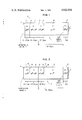
A high efficiency silicon solar cell (1) may be constructed by providing a two-stage drift field emitter (4) with a 1 micron thickness on a drift field base region (10) with a back surface field region (12). The stage (7) of the drift field emitter adjacent to the junction (8) is moderately doped from 1018 to 1016 atoms/cc adjacent the junction to minimize bandgap shrinkage and to maximize carrier lifetime while the stage of the emitter adjacent the surface is highly doped at 1019 atoms/cc to minimize sheet resistance. The drift field is aiding in both the emitter and base regions. The size of the base (10) is less than an effective diffusion length. There is a difference in doping level in the base depending on the conductivity type of the silicon. For n-conductivity type the base is doped 1013 atoms/cc at the pn junction, increasing to 1016 atoms/cc in the drift field region. For p-conductivity type the base is doped 1016 at the junction, increasing to 1018 atoms/cc in the drift field. A back surface field is provided adjacent the ohmic contact (3) on the part of the base remote from the junction by doping to 1020 to 1021 atoms/cc. A passivating antireflective layer (30) is added to the light incident surface. The 1 micron emitter region (4) contains a 0.1 to 0.2 μm thick high conducting region (5) adjacent the antireflective coating (30) on the light incident surface and a drift field region (7) 0.3 to 0.9 μm thick. The base region (10) has a drift field region (9) 20 to 100 μm thick and the overall base region (10) is 50 to 450 μm thick. The back surface field region (12) is 1 μm thick.
Priority Applications (1)
| Application Number | Priority Date | Filing Date | Title |
|---|---|---|---|
| US06/412,424 UST102801I4 (en) | 1978-12-13 | 1982-08-30 | Silicon solar cell |
Applications Claiming Priority (3)
| Application Number | Priority Date | Filing Date | Title |
|---|---|---|---|
| US96888878A | 1978-12-13 | 1978-12-13 | |
| US22936781A | 1981-01-29 | 1981-01-29 | |
| US06/412,424 UST102801I4 (en) | 1978-12-13 | 1982-08-30 | Silicon solar cell |
Related Parent Applications (1)
| Application Number | Title | Priority Date | Filing Date |
|---|---|---|---|
| US22936781A Continuation | 1978-12-13 | 1981-01-29 |
Publications (1)
| Publication Number | Publication Date |
|---|---|
| UST102801I4 true UST102801I4 (en) | 1983-03-01 |
Family
ID=27397947
Family Applications (1)
| Application Number | Title | Priority Date | Filing Date |
|---|---|---|---|
| US06/412,424 Pending UST102801I4 (en) | 1978-12-13 | 1982-08-30 | Silicon solar cell |
Country Status (1)
| Country | Link |
|---|---|
| US (1) | UST102801I4 (en) |
Cited By (2)
| Publication number | Priority date | Publication date | Assignee | Title |
|---|---|---|---|---|
| US5342451A (en) * | 1990-06-07 | 1994-08-30 | Varian Associates, Inc. | Semiconductor optical power receiver |
| US20100037946A1 (en) * | 2006-09-27 | 2010-02-18 | Kyocera Corporation | Solar Cell Element and Method for Manufacturing Solar Cell Element |
-
1982
- 1982-08-30 US US06/412,424 patent/UST102801I4/en active Pending
Cited By (3)
| Publication number | Priority date | Publication date | Assignee | Title |
|---|---|---|---|---|
| US5342451A (en) * | 1990-06-07 | 1994-08-30 | Varian Associates, Inc. | Semiconductor optical power receiver |
| US20100037946A1 (en) * | 2006-09-27 | 2010-02-18 | Kyocera Corporation | Solar Cell Element and Method for Manufacturing Solar Cell Element |
| US8975172B2 (en) * | 2006-09-27 | 2015-03-10 | Kyocera Corporation | Solar cell element and method for manufacturing solar cell element |
Similar Documents
| Publication | Publication Date | Title |
|---|---|---|
| US4135950A (en) | Radiation hardened solar cell | |
| US4838952A (en) | Controlled reflectance solar cell | |
| US4315097A (en) | Back contacted MIS photovoltaic cell | |
| US4072541A (en) | Radiation hardened P-I-N and N-I-P solar cells | |
| US4431858A (en) | Method of making quasi-grain boundary-free polycrystalline solar cell structure and solar cell structure obtained thereby | |
| US4070689A (en) | Semiconductor solar energy device | |
| ATE59116T1 (en) | MULTIPLE JUNCTION SEMICONDUCTOR ARRANGEMENTS. | |
| EP0776051A3 (en) | Structure and fabrication process for an aluminum alloy junction self-aligned back contact silicon solar cell | |
| JPS6453468A (en) | Solar battery | |
| EP0753205A1 (en) | Multiple layer thin film solar cells with buried contacts | |
| EP0837511A3 (en) | Solar cell and method for manufacturing the same | |
| US4106951A (en) | Photovoltaic semiconductor device using an organic material as an active layer | |
| JPS551103A (en) | Semiconductor resistor | |
| US3978511A (en) | Semiconductor diode and method of manufacturing same | |
| FR2549642B1 (en) | SOLAR CELL | |
| US4144094A (en) | Radiation responsive current generating cell and method of forming same | |
| US3812518A (en) | Photodiode with patterned structure | |
| Hebling et al. | HIGH-EFFICIENCY (192%) SILICON THIN-FILM soLAR CELLs wTH INTERDIGITATED EMITTER AND BASE FRONT-CoNTACTs | |
| US4227940A (en) | Solar cell for use in concentrator | |
| UST102801I4 (en) | Silicon solar cell | |
| US4343962A (en) | Oxide charge induced high low junction emitter solar cell | |
| US4112457A (en) | Photovoltaic device having an extended PN junction | |
| JPS60234381A (en) | Solar battery | |
| US3838439A (en) | Phototransistor having a buried base | |
| US4483063A (en) | Oxide charge induced high low junction emitter solar cell |
Legal Events
| Date | Code | Title | Description |
|---|---|---|---|
| STPP | Information on status: patent application and granting procedure in general |
Free format text: DEFENSIVE PUBLICATION OR SIR FILE |