US9977459B1 - Clock generating circuit and associated method - Google Patents
Clock generating circuit and associated method Download PDFInfo
- Publication number
- US9977459B1 US9977459B1 US15/484,149 US201715484149A US9977459B1 US 9977459 B1 US9977459 B1 US 9977459B1 US 201715484149 A US201715484149 A US 201715484149A US 9977459 B1 US9977459 B1 US 9977459B1
- Authority
- US
- United States
- Prior art keywords
- signal
- clock
- frequency
- generating circuit
- circuit
- Prior art date
- Legal status (The legal status is an assumption and is not a legal conclusion. Google has not performed a legal analysis and makes no representation as to the accuracy of the status listed.)
- Active
Links
Images


Classifications
-
- G—PHYSICS
- G06—COMPUTING OR CALCULATING; COUNTING
- G06F—ELECTRIC DIGITAL DATA PROCESSING
- G06F1/00—Details not covered by groups G06F3/00 - G06F13/00 and G06F21/00
- G06F1/04—Generating or distributing clock signals or signals derived directly therefrom
- G06F1/08—Clock generators with changeable or programmable clock frequency
-
- G—PHYSICS
- G04—HOROLOGY
- G04F—TIME-INTERVAL MEASURING
- G04F5/00—Apparatus for producing preselected time intervals for use as timing standards
-
- G—PHYSICS
- G04—HOROLOGY
- G04G—ELECTRONIC TIME-PIECES
- G04G3/00—Producing timing pulses
-
- G—PHYSICS
- G06—COMPUTING OR CALCULATING; COUNTING
- G06F—ELECTRIC DIGITAL DATA PROCESSING
- G06F1/00—Details not covered by groups G06F3/00 - G06F13/00 and G06F21/00
- G06F1/04—Generating or distributing clock signals or signals derived directly therefrom
- G06F1/14—Time supervision arrangements, e.g. real time clock
Definitions
- the present invention relates to a clock generating circuit, and more particularly, to a spread spectrum clock generating circuit and an associated method.
- a clock signal permits the precise timing of events in the microprocessor.
- Typical microprocessors may be synchronized by a free-running oscillator, for example being driven by a crystal, an LC-tuned circuit, or an external clock source.
- the parameters of a clock signal are typically specified for a microprocessor and may include minimum and maximum allowable clock frequencies, tolerances on the high and low voltage levels, maximum rise and fall times on the waveform edges, pulse-width tolerance if the waveform is not a square wave, and the timing relationship between clock phases if two-clock phase signals are needed.
- EMI electromagnetic interference
- the spectral components of the EMI emissions typically have peak amplitudes at harmonics of the fundamental frequency of the clock circuit.
- Other electronic devices e.g., Class D amplifier, modulate the width of square wave pulses as a function of the input audio signal, also have EMI concerns.
- Spread spectrum clock generators could prevent EMI from affecting other circuitries in the integrated circuit; however, conventional spread spectrum clock generators cannot effectively achieve this goal.
- One of the objectives of the present invention is to provide a spread spectrum clock generating circuit and an associated method to solve the abovementioned problem.
- a clock generating circuit comprising: a clock generating circuit, a reference circuit and an adjusting circuit.
- the clock generating circuit is arranged to generate a clock signal.
- the reference circuit coupled to the clock generating circuit is arranged to generate a reference signal to the clock generating circuit according to the clock signal, wherein a frequency of the clock signal is varied according to the reference signal when the reference signal is received by the clock generating circuit.
- the adjusting circuit is arranged to generate an adjusting signal and a trigger signal to the clock generating circuit, wherein the clock generating circuit refers to the trigger signal to decide whether to adjust the clock signal frequency according to the adjusting signal.
- a clock generating method comprising: generating a reference signal according to a clock signal, wherein a frequency of the clock signal is varied according to the reference signal; generating an adjusting signal and a trigger signal; and referring to the trigger signal to decide whether to adjust the clock signal frequency according to the adjusting signal.
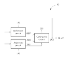
- FIG. 1 is a diagram illustrating a clock generating circuit according to an embodiment of the present invention.
- FIG. 2 is a diagram illustrating a generating circuit of the clock generating circuit according to an embodiment of the present invention.
- FIG. 3 is diagram illustrating a digital controlled voltage generating circuit of the generating circuit according to an embodiment of the present invention.
- FIG. 4 is a diagram illustrating a reference circuit of the clock generating circuit according to an embodiment of the present invention.
- FIG. 5 is a diagram illustrating a reference signal comprising a first reference signal, a second reference signal and a third reference signal, and the clock signal frequency according to an embodiment of the present invention.
- FIG. 6 is a diagram illustrating an adjusting circuit of the clock generating circuit according to an embodiment of the present invention.
- FIG. 7 is a diagram illustrating an adjusting signal and a trigger signal generated by the adjusting circuit according to an embodiment of the present invention.
- FIG. 1 is a diagram illustrating a clock generating circuit 10 according to an embodiment of the present invention.
- the clock generating circuit 10 comprises a generating circuit 110 , a reference circuit 120 , and an adjusting circuit 130 , wherein the generating circuit 110 is arranged to generate a clock signal CLK at an output terminal OUT of the clock generating circuit 10 , the reference circuit 120 is arranged to generate a reference signal REF to the generating circuit 110 according to the clock signal CLK, and the adjusting circuit 130 is arranged to generate an adjusting signal ADJ and a trigger signal TRI to the generating circuit 110 .
- a frequency of the clock signal (marked CLK(f)) is varied according to the reference signal REF.
- the generating circuit 110 refers to the trigger signal TRI to determine whether to adjust the frequency of the clock signal CLK according to the adjusting signal ADJ.
- FIG. 2 is a diagram illustrating the generating circuit 110 of the clock generating circuit 10 according to an embodiment of the present invention.
- the generating circuit 110 comprises a decoder 210 , a digital controlled voltage generating circuit 220 , and a comparing circuit 230 .
- the decoder 210 is arranged to decode the reference signal REF for outputting a reference code REF_code, and further arranged to decode the adjusting signal ADJ for outputting an adjusting code ADJ_code when the trigger signal TRI is a specific value in order to trigger the decoder 210 .
- FIG. 1 is a diagram illustrating the generating circuit 110 of the clock generating circuit 10 according to an embodiment of the present invention.
- the generating circuit 110 comprises a decoder 210 , a digital controlled voltage generating circuit 220 , and a comparing circuit 230 .
- the decoder 210 is arranged to decode the reference signal REF for outputting a reference code REF_code, and further arranged to
- the digital controlled voltage generating circuit 220 comprises a digital controlled current generating circuit 221 and a capacitor Cc, wherein the digital controlled current generating circuit 221 generates a digital controlled current I digital to the capacitor Cc for generating a digital controlled voltage V digital .
- the digital controlled current I digital is generated according to the reference code REF_code or the adjusting code ADJ_code.
- the comparing circuit 230 comprises comparators 231 and 232 and a latch circuit 233 , wherein the comparator 231 and 232 are arranged to compare the digital controlled voltage V digital with a first reference voltage V H and a second reference voltage V L to respectively generate comparing results COM H and COM L to the latch circuit 233 .
- the latch circuit 233 receives the comparing results COM H and COM L to generate the clock signal CLK.
- the latch circuit 233 is implemented by a SR latch in this embodiment; however, this is only for illustrative purposes and not a limitation of the present invention. Those skilled in the art should readily understand that, as well two comparators and a latch, there are other implementations of generating a clock signal.
- FIG. 3 is a diagram illustrating the digital controlled current generating circuit 221 of the generating circuit 110 according to an embodiment of the present invention.
- the reference code REF_code and the adjusting code ADJ_code are composed of two bits, and are respectively represented as bits B 1 and B 2 in FIG. 3 .
- the digital controlled current generating circuit 221 comprises NMOS transistors MN 1 and MN 2 . As shown in FIG.
- a gate terminal of the NMOS transistor MN 1 is coupled to the bit B 1 while a gate terminal of the NMOS transistor MN 2 is coupled to the bit B 2
- a drain terminal of the NMOS transistor MN 1 is coupled to a current source I 1 while a drain terminal of the NMOS transistor MN 2 is coupled to a current source I 2
- the digital controlled current is generated from source terminals of the NMOS transistor MN 1 and MN 2 .
- a current drained from the current source I 1 is I while a current drained from the current source I 2 is 2*I.
- the current drained from the current source I 2 can be varied with multiple of I.
- the reference code REF_code or the adjusting code ADJ_code are composed of the bits B 1 and B 2 in this embodiment.
- the reference code REF_code or the adjusting code ADJ_code can also be composed of more than two bits in other embodiments.
- the digital controlled current generating circuit 221 should comprise more NMOS transistors.
- the bits B 1 and B 2 are used for determining whether to turn on the NMOS transistors MN 1 and MN 2 , respectively.
- the bits B 1 and B 2 determine the value of the digital controlled current I digital and the digital controlled voltage V digital accordingly.
- a stronger digital controlled current I digital means the digital controlled voltage V digital will have a higher voltage level which indirectly causes the clock signal CLK to have a higher frequency. More specifically, when a value of the bits B 2 , B 1 generated by the decoder 210 is (0, 0), so that both the NMOS transistors MN 1 and MN 2 will be turned off, the digital controlled current I digital is at its minimum value causing the clock signal CLK to have a lowest frequency.
- FIG. 4 is a diagram illustrating the reference circuit 120 of the clock generating circuit 10 according to an embodiment of the present invention.
- the reference circuit 120 comprises a frequency dividing circuit 410 , wherein the frequency dividing circuit 410 performs a frequency division on the clock signal CLK to generate the reference signal REF.
- the reference signal REF is composed of a first reference signal REF 1 , a second reference signal REF 2 and a third reference signal REF 3 .
- the frequency dividing circuit comprises frequency dividers 411 , 412 and 413 , all having frequency dividing factors of 2, which generate the first reference signal REF 1 , the second reference signal REF 2 and the third reference signal REF 3 .
- the frequency of the first reference signal REF 1 is half the frequency of the clock signal CLK (marked as f/2), the frequency of the second reference signal REF 2 is a quarter of the frequency of the clock signal CLK (marked as f/4), and the frequency of the third reference signal REF 3 is an eighth of the frequency of the clock signal CLK (marked as f/8).
- FIG. 5 is a diagram illustrating the reference signal REF comprising the first reference signal REF 1 , the second reference signal REF 2 and the third reference signal REF 3 , and the clock signal frequency, according to an embodiment of the present invention.
- the first reference signal REF 1 being half the frequency of the clock signal CLK
- the second reference signal REF 2 being a quarter of the frequency of the clock signal CLK are decoded by the decoder 210 shown in FIG. 2 for generating the reference code REF_code composed of the bits B 1 and B 2 .
- the reference code REF_code will be generated as ‘00’.
- the reference code REF_code will be generated as ‘01’.
- the reference code REF_code will be generated as ‘10’.
- the reference code REF_code will be generated as ‘11’.
- the reference code REF_code generated by the decoder 210 will be inverted.
- the reference code REF_code will be generated as ‘11’, and so on.
- the frequency of the clock signal CLK is determined by the reference code REF_code. Therefore, when the reference code REF_code is varied periodically and repeatedly, the frequency of the clock signal will also be varied periodically and repeatedly, as shown in FIG. 5 .
- the frequency of the clock signal is varied periodically and repeatedly as a sawtooth curve; however, in other embodiments, the frequency of the clock signal has periodically and repeatedly curves, e.g., a ramp curve, or a step-wise continuous sinusoidal curve.
- FIG. 6 is a diagram illustrating the adjusting circuit 130 of the clock generating circuit 10 according to an embodiment of the present invention.
- the adjusting circuit 130 comprises a random signal generating circuit 610 and a logic circuit 620 .
- the random signal generating circuit 610 is arranged to generate a random signal RAM comprising a plurality of bits R 1 , R 2 , . . . R n , wherein the adjusting signal is generated according to a first part of the plurality of bits R 1 , R 2 , . . . R n of the random signal RAM and the trigger signal TRI is generated according to a second part of the plurality of bits R 1 , R 2 , . . . R n of the random signal RAM.
- the random signal generating circuit 610 is implemented by a linear feedback shift register (LFSR) for randomly generating the random signal RAM according to the clock signal CLK.
- LFSR linear feedback shift register
- the adjusting signal ADJ is directly extracted from the first part of the plurality of bits R 1 , R 2 , . . . R n .
- the adjusting code ADJ_code comprises only two bits; therefore, the adjusting signal ADJ is extracted from two of the plurality of bits R 1 , R 2 , . . . R n .
- the bits (R 5 , R 4 ) shown in FIG. 6 are outputted as the adjusting signal ADJ.
- the logic circuit 620 is arranged to generate the trigger signal TRI according to the second part of the plurality of bits R 1 , R 2 , . . . R n of the random signal RAM.
- the second part of the plurality of R 1 , R 2 , . . . R n comprises the bits (R 3 ,R 2 ,R 1 ) (this is only for illustrative purposes and not a limitation of the present invention).
- the logic circuit 620 comprises an ADD gate 621 for receiving the bits (R 3 ,R 2 ,R 1 ) as inputs to generate the trigger signal TRI.
- the trigger signal TRI is the specific value (i.e. logic ‘high’) for triggering the decoder 210 to decode the adjusting signal ADJ in order to generate the adjusting code ADJ_code.
- the logic circuit 620 is implemented by the ADD gate 621 for receiving the bits (R 3 ,R 2 ,R 1 ); however, the goal of the trigger signal TRI is only for randomly determining whether the frequency of the clock signal CLK should be adjusted according to the adjusting signal ADJ.
- the logic circuit 620 can be implemented by different logic gates and receive more or less than three bits from the plurality of bits R 1 , R 2 , . . .
- the specific value of the trigger signal TRI is not limited to be logic ‘high’.
- the logic circuit 620 can be implemented by a NAND gate. When the bits (R 3 ,R 2 ,R 1 ) are all logic ‘high’, the trigger signal TRI has the specific value (i.e. logic ‘low’).
- the logic circuit 620 can be implemented by a buffer for receiving only one bit (e.g. the bit R 3 ) from the plurality of bits R 1 , R 2 , . . . R n and outputting the bit R 3 as the trigger signal TRI.
- the decoder 210 will be triggered when the trigger signal TRI is logic ‘low’.
- the implementation of the logic circuit 620 and the number of bits received by the logic circuit 620 are not limitations of the present invention.
- FIG. 7 is a diagram illustrating the adjusting signal ADJ and the trigger signal TRI generated by the adjusting circuit 130 according to an embodiment of the present invention.
- the trigger signal has the specific value (assume the specific value is set to be the logic ‘high’), at the time points t 0 and t 1 , for example.
- the decoder 210 is triggered by the trigger signal TRI and receives the adjusting signal ADJ comprising the bits (R 5 R 4 ), and decodes the adjusting signal ADJ to generate the adjusting code ADJ_code (whose bits value is ‘10’) to the digital controlled voltage generating circuit 220 .
- the frequency of the clock signal CLK is adjusted according to the adjusting code ADJ_code at the time point t 1 as shown in FIG. 7 .
- the decoder 210 is triggered by the trigger signal TRI and receives the adjusting signal ADJ comprising the bits (R 5 R 4 ), and decodes the adjusting signal ADJ to generate the adjusting code ADJ_code (whose bits value is ‘11’) to the digital controlled voltage generating circuit 220 .
- the frequency of the clock signal CLK is adjusted according to the adjusting code ADJ_code at the time point t 0 as shown in FIG. 7 .
- the frequency of the clock signal CLK is varied repeatedly and periodically. Furthermore, by randomly generating the adjusting signal ADJ and the trigger signal TRI, the frequency of the clock signal CLK can also be adjusted randomly. In this way, the Electromagnetic Interference (EMI) in response to the clock signal CLK can be effectively reduced.
- EMI Electromagnetic Interference
Landscapes
- Physics & Mathematics (AREA)
- Engineering & Computer Science (AREA)
- General Physics & Mathematics (AREA)
- Theoretical Computer Science (AREA)
- General Engineering & Computer Science (AREA)
- Manipulation Of Pulses (AREA)
Abstract
Description
Claims (18)
Priority Applications (1)
| Application Number | Priority Date | Filing Date | Title |
|---|---|---|---|
| US15/484,149 US9977459B1 (en) | 2017-04-11 | 2017-04-11 | Clock generating circuit and associated method |
Applications Claiming Priority (1)
| Application Number | Priority Date | Filing Date | Title |
|---|---|---|---|
| US15/484,149 US9977459B1 (en) | 2017-04-11 | 2017-04-11 | Clock generating circuit and associated method |
Publications (1)
| Publication Number | Publication Date |
|---|---|
| US9977459B1 true US9977459B1 (en) | 2018-05-22 |
Family
ID=62125410
Family Applications (1)
| Application Number | Title | Priority Date | Filing Date |
|---|---|---|---|
| US15/484,149 Active US9977459B1 (en) | 2017-04-11 | 2017-04-11 | Clock generating circuit and associated method |
Country Status (1)
| Country | Link |
|---|---|
| US (1) | US9977459B1 (en) |
Citations (2)
| Publication number | Priority date | Publication date | Assignee | Title |
|---|---|---|---|---|
| US6737904B1 (en) * | 1999-11-12 | 2004-05-18 | Koninklijke Philips Electronics N.V. | Clock circuit, GSM phone, and methods of reducing electromagnetic interference |
| US8831064B1 (en) * | 2007-06-13 | 2014-09-09 | Xilinx, Inc. | Method of and circuit for generating a spread spectrum clock signal |
-
2017
- 2017-04-11 US US15/484,149 patent/US9977459B1/en active Active
Patent Citations (2)
| Publication number | Priority date | Publication date | Assignee | Title |
|---|---|---|---|---|
| US6737904B1 (en) * | 1999-11-12 | 2004-05-18 | Koninklijke Philips Electronics N.V. | Clock circuit, GSM phone, and methods of reducing electromagnetic interference |
| US8831064B1 (en) * | 2007-06-13 | 2014-09-09 | Xilinx, Inc. | Method of and circuit for generating a spread spectrum clock signal |
Similar Documents
| Publication | Publication Date | Title |
|---|---|---|
| US6452432B2 (en) | Signal processing circuits having a pair of delay locked loop (DLL) circuits for adjusting a duty-cycle of a periodic digital signal and methods of operating same | |
| US8058913B2 (en) | DLL-based multiphase clock generator | |
| US8878582B2 (en) | Apparatus and method for duty cycle calibration | |
| US7576581B2 (en) | Circuit and method for correcting duty cycle | |
| US20090058483A1 (en) | Duty cycle correcting circuit and method | |
| US7737797B2 (en) | Controllable oscillating system and related method for selectively adjusting currents passing through cross-coupling driving device | |
| US12244316B2 (en) | Semiconductor device having duty-cycle corrector | |
| US6747496B2 (en) | DLL-(delay-locked-loop) circuit | |
| US7233210B2 (en) | Spread spectrum clock generator | |
| US8094698B2 (en) | Method for generating a spread spectrum clock and apparatus thereof | |
| US9977459B1 (en) | Clock generating circuit and associated method | |
| KR102387233B1 (en) | Buffer Circuit | |
| US8138800B2 (en) | Phase detecting circuit and PLL circuit | |
| US7764096B2 (en) | DLL circuit and method of controlling the same | |
| CN115051697B (en) | Signal output circuit and delayed signal output circuit | |
| US7288979B2 (en) | Semiconductor equipment | |
| US8278985B2 (en) | Synchronization circuit | |
| US9628091B1 (en) | Phase detector for clock data recovery circuit | |
| JP5319230B2 (en) | Semiconductor integrated circuit | |
| TWI635709B (en) | Clock generating circuit | |
| US7317359B2 (en) | Circuits and methods for phase locked loop lock window detection | |
| US9473147B2 (en) | Frequency dividing apparatus and related method | |
| KR101208026B1 (en) | Edge combiner, frequency multiplier and method of frequency multiplying using the edge combiner | |
| US10511292B2 (en) | Oscillator | |
| US11545966B2 (en) | Injection locking oscillator circuit and operating method |
Legal Events
| Date | Code | Title | Description |
|---|---|---|---|
| AS | Assignment |
Owner name: ELITE SEMICONDUCTOR MEMORY TECHNOLOGY INC., TAIWAN Free format text: ASSIGNMENT OF ASSIGNORS INTEREST;ASSIGNORS:CHAN, CHIN-TUNG;TSAO, SZU-CHUN;SHIH, DENG-YAO;REEL/FRAME:041952/0211 Effective date: 20170407 |
|
| STCF | Information on status: patent grant |
Free format text: PATENTED CASE |
|
| MAFP | Maintenance fee payment |
Free format text: PAYMENT OF MAINTENANCE FEE, 4TH YR, SMALL ENTITY (ORIGINAL EVENT CODE: M2551); ENTITY STATUS OF PATENT OWNER: SMALL ENTITY Year of fee payment: 4 |
|
| FEPP | Fee payment procedure |
Free format text: ENTITY STATUS SET TO UNDISCOUNTED (ORIGINAL EVENT CODE: BIG.); ENTITY STATUS OF PATENT OWNER: LARGE ENTITY |
|
| AS | Assignment |
Owner name: ELITE SEMICONDUCTOR MICROELECTRONICS TECHNOLOGY INC., TAIWAN Free format text: CHANGE OF NAME;ASSIGNOR:ELITE SEMICONDUCTOR MEMORY TECHNOLOGY INC.;REEL/FRAME:071703/0241 Effective date: 20250317 |
|
| MAFP | Maintenance fee payment |
Free format text: PAYMENT OF MAINTENANCE FEE, 8TH YEAR, LARGE ENTITY (ORIGINAL EVENT CODE: M1552); ENTITY STATUS OF PATENT OWNER: LARGE ENTITY Year of fee payment: 8 |