US9960248B2 - Fin-based RF diodes - Google Patents
Fin-based RF diodes Download PDFInfo
- Publication number
- US9960248B2 US9960248B2 US15/616,653 US201715616653A US9960248B2 US 9960248 B2 US9960248 B2 US 9960248B2 US 201715616653 A US201715616653 A US 201715616653A US 9960248 B2 US9960248 B2 US 9960248B2
- Authority
- US
- United States
- Prior art keywords
- fin
- upper portion
- top surface
- region
- type dopant
- Prior art date
- Legal status (The legal status is an assumption and is not a legal conclusion. Google has not performed a legal analysis and makes no representation as to the accuracy of the status listed.)
- Active
Links
Images


Classifications
-
- H01L29/6609—
-
- H—ELECTRICITY
- H10—SEMICONDUCTOR DEVICES; ELECTRIC SOLID-STATE DEVICES NOT OTHERWISE PROVIDED FOR
- H10W—GENERIC PACKAGES, INTERCONNECTIONS, CONNECTORS OR OTHER CONSTRUCTIONAL DETAILS OF DEVICES COVERED BY CLASS H10
- H10W10/00—Isolation regions in semiconductor bodies between components of integrated devices
- H10W10/01—Manufacture or treatment
- H10W10/011—Manufacture or treatment of isolation regions comprising dielectric materials
- H10W10/014—Manufacture or treatment of isolation regions comprising dielectric materials using trench refilling with dielectric materials, e.g. shallow trench isolations
-
- H01L21/26513—
-
- H01L21/76224—
-
- H01L27/0814—
-
- H01L29/0649—
-
- H01L29/861—
-
- H—ELECTRICITY
- H10—SEMICONDUCTOR DEVICES; ELECTRIC SOLID-STATE DEVICES NOT OTHERWISE PROVIDED FOR
- H10D—INORGANIC ELECTRIC SEMICONDUCTOR DEVICES
- H10D62/00—Semiconductor bodies, or regions thereof, of devices having potential barriers
- H10D62/10—Shapes, relative sizes or dispositions of the regions of the semiconductor bodies; Shapes of the semiconductor bodies
- H10D62/117—Shapes of semiconductor bodies
-
- H—ELECTRICITY
- H10—SEMICONDUCTOR DEVICES; ELECTRIC SOLID-STATE DEVICES NOT OTHERWISE PROVIDED FOR
- H10D—INORGANIC ELECTRIC SEMICONDUCTOR DEVICES
- H10D62/00—Semiconductor bodies, or regions thereof, of devices having potential barriers
- H10D62/10—Shapes, relative sizes or dispositions of the regions of the semiconductor bodies; Shapes of the semiconductor bodies
- H10D62/124—Shapes, relative sizes or dispositions of the regions of semiconductor bodies or of junctions between the regions
- H10D62/125—Shapes of junctions between the regions
-
- H—ELECTRICITY
- H10—SEMICONDUCTOR DEVICES; ELECTRIC SOLID-STATE DEVICES NOT OTHERWISE PROVIDED FOR
- H10D—INORGANIC ELECTRIC SEMICONDUCTOR DEVICES
- H10D8/00—Diodes
-
- H—ELECTRICITY
- H10—SEMICONDUCTOR DEVICES; ELECTRIC SOLID-STATE DEVICES NOT OTHERWISE PROVIDED FOR
- H10D—INORGANIC ELECTRIC SEMICONDUCTOR DEVICES
- H10D8/00—Diodes
- H10D8/01—Manufacture or treatment
- H10D8/045—Manufacture or treatment of PN junction diodes
-
- H—ELECTRICITY
- H10—SEMICONDUCTOR DEVICES; ELECTRIC SOLID-STATE DEVICES NOT OTHERWISE PROVIDED FOR
- H10D—INORGANIC ELECTRIC SEMICONDUCTOR DEVICES
- H10D8/00—Diodes
- H10D8/01—Manufacture or treatment
- H10D8/051—Manufacture or treatment of Schottky diodes
-
- H—ELECTRICITY
- H10—SEMICONDUCTOR DEVICES; ELECTRIC SOLID-STATE DEVICES NOT OTHERWISE PROVIDED FOR
- H10D—INORGANIC ELECTRIC SEMICONDUCTOR DEVICES
- H10D8/00—Diodes
- H10D8/60—Schottky-barrier diodes
-
- H—ELECTRICITY
- H10—SEMICONDUCTOR DEVICES; ELECTRIC SOLID-STATE DEVICES NOT OTHERWISE PROVIDED FOR
- H10W—GENERIC PACKAGES, INTERCONNECTIONS, CONNECTORS OR OTHER CONSTRUCTIONAL DETAILS OF DEVICES COVERED BY CLASS H10
- H10W10/00—Isolation regions in semiconductor bodies between components of integrated devices
- H10W10/10—Isolation regions comprising dielectric materials
- H10W10/17—Isolation regions comprising dielectric materials formed using trench refilling with dielectric materials, e.g. shallow trench isolations
Definitions
- the present disclosure relates generally to designing and fabricating integrated circuit (IC) devices.
- the present disclosure is particularly applicable to radio frequency (RF) diodes in fin-type devices, particularly for the 14 nanometer (nm) technology node and beyond.
- RF radio frequency
- a diode may be switched from a conducting state (forward-bias) to a non-conducting (reverse-bias) state.
- the speed at which the switching can occur may be limited by the time it takes to remove or add electrical charge to/from the depletion region of the diode.
- the time may be based on two parameters: the lifetime of the carriers, ⁇ n and ⁇ p, and the capacitance of the junction area.
- excess minority carriers holes in the n region and electrons in the p region
- a larger junction area allows for a larger current to flow, and the series resistance drops.
- Conventional fin-based diodes formed by growing embedded silicon germanium (eSiGe) at the top of p+ fins, with the p+/n-well junction at the interface between the fin and the eSiGe, suffer from non-ideality and leakage, among other things.
- the junction can be optimized by making the entire fin of grown eSiGe.
- the optimized diode has low leakage current and an excellent ideality range, even at increased temperatures.
- RF diodes have characteristics that make them particularly attractive in IC devices. For example, an RF diode has an increased depletion region width over a conventional diode, which leads to lowering of capacitance. In addition, for small signals at high frequencies the stored carriers within the intrinsic layer are not completely swept by the RF signal or recombined (due to a large Fin height region). At such frequencies there is no rectification or distortion, and the RF diode characteristic is that of a linear resistor, which introduces no distortion or rectification. The RF diode resistance is governed by the DC bias applied. In this way it is possible to use the device as an effective RF switch or variable resistor for an attenuator producing far less distortion than ordinary PN junction diodes.
- RF diodes implemented in fin-type devices not only need to meet performance characteristics such as leakage current, ideality, and breakdown voltage, but also need to prevent increases in parasitic resistance or capacitance.
- the fin width is reduced, thereby reducing the junction area in reverse biasing mode and increasing parasitic capacitance and resistance.
- An aspect of the present disclosure is a method for forming a fin-based RF diode with improved performance characteristics.
- Another aspect of the present disclosure is a device including a fin-based RF diode with improved performance characteristics.
- some technical effects may be achieved in part by a method including forming fins over a substrate, separated from each other, each fin having a lower portion and an upper portion; forming shallow trench isolation (STI) regions over the substrate, between the lower portions of adjacent fins; implanting the lower portion of each fin with a first-type dopant; implanting the upper portion of each fin, above the STI region, with the first-type dopant; forming a junction region around a depletion region and along exposed sidewalls and a top surface of the upper portion of each fin; and forming a contact on exposed sidewalls and a top surface of each junction region.
- STI shallow trench isolation
- the first-type dopant includes a p-type dopant.
- Another aspect includes forming the junction region by plasma doping or with an energy of 0.1 to 0.5 KeV.
- One aspect includes implanting the lower portion of each fin to a higher concentration level of the first-type dopant than the upper portion of each fin.
- An additional aspect includes forming the upper portion of each fin with a top surface narrower than a bottom surface.
- a further aspect includes forming an active depletion region between the depletion region and the lower portion of each fin.
- Another aspect includes increasing a forward current capacity by increasing a concentration level of the diode cathode dopant.
- One aspect includes increasing a forward current capacity by increasing an area of the junction region.
- a further aspect includes forming the junction region by implanting the exposed sidewalls and the top surface of each fin with a diode cathode dopant.
- An additional aspect includes forming a layer of silicide material on the exposed sidewalls and the top surface of each fin for forming the junction region.
- Another aspect includes reducing a charge capacitance in the depletion region by reducing a size of the depletion region.
- Another aspect of the present disclosure includes a device including: fins over a substrate, separated from each other, each fin having a lower portion and an upper portion; shallow trench isolation (STI) regions over the substrate, between the lower portions of adjacent fins; the lower portion of each fin implanted with a first-type dopant; the upper portion of each fin, above the STI region, implanted with the first-type dopant; a junction region around a depletion region and along exposed sidewalls and a top surface of the upper portion of each fin; and a contact on a top surface of each junction region.
- STI shallow trench isolation
- the first-type dopant includes a p-type dopant.
- each fin is implanted with the first-type dopant to a higher concentration level than the upper portion of each fin.
- each fin has a top surface narrower than a bottom surface.
- Another aspect includes an active depletion region between the depletion region and the lower portion of each fin.
- junction region including the exposed sidewalls and the top surface of each fin, is implanted with a diode cathode dopant.
- the junction region includes a layer of silicide gate material on the exposed sidewalls and the top surface of each fin.
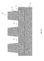
- FIG. 1A illustrates a top view of a layout of Fin-based RF diodes, in accordance with an exemplary embodiment
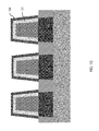
- FIGS. 1B through 1G illustrate cross-sectional views of a process flow for forming Fin-based RF diodes, in accordance with an exemplary embodiment.
- the present disclosure addresses the problems of reduced junction area and increased parasitic resistance and capacitance attendant upon scaling down fin-based RF diodes.
- the present disclosure addresses and solves such problems, for instance, by, inter alia, forming fins with optimized fin-widths for larger diode junction regions and lower diode series resistance resulting in higher current.
- Methodology in accordance with embodiments of the present disclosure includes forming fins over a substrate, separated from each other, each fin having a lower portion and an upper portion.
- STI regions are formed over the substrate, between the lower portions of adjacent fins.
- the lower and upper portions of each fin are implanted with a first-type dopant.
- a junction region is formed around a depletion region and along exposed sidewalls and a top surface of the upper portion of each fin.
- a contact is formed on exposed sidewalls and a top surface of each junction region.
- FIG. 1A illustrates a substrate 101 (e.g. p-type) and Fin-based RF diodes including fins 105 separated from each other by STI regions 107 over the substrate 101 .
- Junction regions 109 may be formed on exposed sidewalls and the top surface of each fin 105 .
- a contact layer 111 may be formed on sidewalls and the top surface of each junction region 109 .
- the line 1 B- 1 B′ illustrates the cut-line for the cross-sectional views of the method of forming the Fin-based RF diodes of FIG. 1A , beginning with FIG. 1B .
- FIG. 1B illustrates the substrate 101 and fins 105 separated from each other over the substrate 101 .
- the fins 105 include a lower portion 113 and an upper portion 115 .
- the upper portion 115 of each fin 105 may be formed with a top surface 117 narrower than a bottom surface 119 , for example, by using spacer merging and etching processes.
- STI regions 107 are formed over the substrate 101 and between the lower portions 113 of adjacent fins 105 .
- each fin 105 are implanted with a first-type dopant (e.g. a p-type dopant) such as boron, wherein the lower portions 113 may be implanted to a higher concentration level than the concentration level at the upper portions 115 of each fin 105 .
- a first-type dopant e.g. a p-type dopant
- the doped lower portion may have a concentration of 1e14 to 1e16, whereas the upper portion may have a concentration of 1e12 to 1e14.
- a junction region 121 may be formed around a depletion region 123 and along exposed sidewalls 125 and a top surface 127 of the upper portion 115 of each fin 105 .
- the light doping in region 123 allows depleting to spread more readily.
- the junction may be formed by plasma doping or low energy doping, e.g. at an energy of 0.1 to 0.5 KeV, with a second-type dopant (e.g. an n-type dopant, such as phosphorous).
- An active depletion region 129 of current flow is formed between the depletion region 123 and the lower portion 113 of each fin 105 .
- a capacitance in the depletion region 123 may be reduced by reducing a size of the depletion region 123 .
- An effective depletion region, which can affect the capacitance, may depend on a base of active depletion region 129 .
- a complementary doping (with the first-type dopant being an n-type and the second-type dopant being a p-type) can be alternatively used for P+/n type diode formation.
- Merging of depletion region 123 from both sides of the junction can result in a fixed narrow depletion region 123 even without doping of the junction region 121 .
- the effective area of the junction is twice the height (h) 135 plus the width of the top (ft) 133 .
- Forward current increases with junction area.
- Higher N+ doping in the junction area also increases current.
- a higher drive current may be achieved by a having a SiGe depletion region 123 .
- the depletion region 123 may be depleted and non-depleted.
- the off-state capacitance, when the depletion region is merged is the width of the bottom (fb) 131 .
- the junction width is about 48 nm and for a conventional fin based diode, it is about 13 nm.
- the effective junction width or the sum of two times the height (e.g. 40 nm) and the top width (ft) (e.g. 6 nm) equals 86
- the gain over a planar diode is about two times and over a conventional fin-type diode is about seven times at the current technology node, which increases as the technologies are scaled down.
- the depletion width (d) can increase from, for example, 5 nm to 42 nm, and capacitance is proportional to 1/d, the device of FIG. 1A has a reduction in capacitance of about 8 times, assuming the junctions are close to the surface.
- the depletion region 123 in general grows even further in lightly doped region, but its growth is limited by another region growing from sidewalls 125 . After merge, the depletion region 123 may remain the same (e.g. not grow) irrespective of a forward or reverse bias application.
- the depletion region 123 may have a fixed capacitance for any given bias after a fixed bias voltage. A smaller depletion region 123 may lead to a smaller capacitance as it depends upon the top 133 to bottom 131 of the depletion region 123 . In switching application, charge can be easily swept from on to off states. Active area of the cap (e.g. 2 ⁇ 125+127) depends upon the base 129 active region 131 of the cap resulting in lower capacitance for a smaller area.
- a narrower fin-width may result in an increase in parasitic resistance, which may influence performance characteristics of an RF diode.
- An optimum fin-width may be determined based on desired performance characteristics of an RF diode. Additionally, performance of the RF diode may be further optimized by determining optimum doping parameters.
- a base region under the cap may have a higher doping level for a lower parasitic resistance.
- the junction region 121 may be formed by forming a layer of silicide material 137 on the exposed sidewalls 125 and the top surface 127 of each fin 105 .
- Titanium silicide (TiSi), nickel silicide (NiSi), tungsten silicide (WSi), etc. provide Schottky diode like features and significantly increase the diode speed as well as multiply the forward current.
- a contact layer 139 (e.g. titanium-silicide) may be formed on exposed sidewalls and top surface of each junction region 121 .
- the embodiments of the present disclosure can achieve several technical effects including increasing the width of the diode depletion region (e.g. wider than a conventional diode) for lowering the capacitance. Also, the transition region from the on-state to the off-state shows fast switching from a high to a low capacitance (the capacitance acts as an RC delay). Furthermore, the embodiments enjoy utility in various industrial applications as, for example, microprocessors, smart phones, mobile phones, cellular handsets, set-top boxes, DVD recorders and players, automotive navigation, printers and peripherals, networking and telecom equipment, gaming systems, digital cameras, or other devices utilizing logic or high-voltage technology nodes. The present disclosure therefore enjoys industrial applicability in any of various types of highly integrated semiconductor devices, including devices that use SRAM cells (e.g., liquid crystal display (LCD) drivers, digital processors, etc.)
- SRAM cells liquid crystal display (LCD) drivers, digital processors, etc.
Landscapes
- Electrodes Of Semiconductors (AREA)
- Metal-Oxide And Bipolar Metal-Oxide Semiconductor Integrated Circuits (AREA)
Abstract
Description
Claims (18)
Priority Applications (1)
| Application Number | Priority Date | Filing Date | Title |
|---|---|---|---|
| US15/616,653 US9960248B2 (en) | 2016-07-25 | 2017-06-07 | Fin-based RF diodes |
Applications Claiming Priority (2)
| Application Number | Priority Date | Filing Date | Title |
|---|---|---|---|
| US15/218,318 US9704966B1 (en) | 2016-07-25 | 2016-07-25 | Fin-based RF diodes |
| US15/616,653 US9960248B2 (en) | 2016-07-25 | 2017-06-07 | Fin-based RF diodes |
Related Parent Applications (1)
| Application Number | Title | Priority Date | Filing Date |
|---|---|---|---|
| US15/218,318 Division US9704966B1 (en) | 2016-07-25 | 2016-07-25 | Fin-based RF diodes |
Publications (2)
| Publication Number | Publication Date |
|---|---|
| US20180026113A1 US20180026113A1 (en) | 2018-01-25 |
| US9960248B2 true US9960248B2 (en) | 2018-05-01 |
Family
ID=59257081
Family Applications (2)
| Application Number | Title | Priority Date | Filing Date |
|---|---|---|---|
| US15/218,318 Active US9704966B1 (en) | 2016-07-25 | 2016-07-25 | Fin-based RF diodes |
| US15/616,653 Active US9960248B2 (en) | 2016-07-25 | 2017-06-07 | Fin-based RF diodes |
Family Applications Before (1)
| Application Number | Title | Priority Date | Filing Date |
|---|---|---|---|
| US15/218,318 Active US9704966B1 (en) | 2016-07-25 | 2016-07-25 | Fin-based RF diodes |
Country Status (1)
| Country | Link |
|---|---|
| US (2) | US9704966B1 (en) |
Cited By (1)
| Publication number | Priority date | Publication date | Assignee | Title |
|---|---|---|---|---|
| US20180006019A1 (en) * | 2016-04-27 | 2018-01-04 | Globalfoundries Inc. | Fin diode with increased junction area |
Families Citing this family (2)
| Publication number | Priority date | Publication date | Assignee | Title |
|---|---|---|---|---|
| US11018230B1 (en) * | 2019-12-20 | 2021-05-25 | Nxp B.V. | Semiconductor devices with a mixed crystal region |
| US11581399B2 (en) * | 2020-06-30 | 2023-02-14 | Texas Instruments Incorporated | Gate implant for reduced resistance temperature coefficient variability |
Citations (6)
| Publication number | Priority date | Publication date | Assignee | Title |
|---|---|---|---|---|
| US20080185691A1 (en) * | 2007-02-01 | 2008-08-07 | Kangguo Cheng | Fin Pin Diode |
| US20100202186A1 (en) | 2009-02-12 | 2010-08-12 | Mitsuru Sato | Semiconductor memory device, method of manufacturing the same, and method of screening the same |
| US20110001169A1 (en) | 2009-07-01 | 2011-01-06 | International Business Machines Corporation | Forming uniform silicide on 3d structures |
| US20150014809A1 (en) * | 2013-07-15 | 2015-01-15 | United Microelectronics Corp. | Fin diode structure |
| US20150194419A1 (en) * | 2014-01-06 | 2015-07-09 | Globalfoundries Inc. | Three-dimensional electrostatic discharge semiconductor device |
| US9472620B1 (en) * | 2015-09-04 | 2016-10-18 | Taiwan Semiconductor Manufacturing Co., Ltd. | Semiconductor device including fin structures and manufacturing method thereof |
-
2016
- 2016-07-25 US US15/218,318 patent/US9704966B1/en active Active
-
2017
- 2017-06-07 US US15/616,653 patent/US9960248B2/en active Active
Patent Citations (6)
| Publication number | Priority date | Publication date | Assignee | Title |
|---|---|---|---|---|
| US20080185691A1 (en) * | 2007-02-01 | 2008-08-07 | Kangguo Cheng | Fin Pin Diode |
| US20100202186A1 (en) | 2009-02-12 | 2010-08-12 | Mitsuru Sato | Semiconductor memory device, method of manufacturing the same, and method of screening the same |
| US20110001169A1 (en) | 2009-07-01 | 2011-01-06 | International Business Machines Corporation | Forming uniform silicide on 3d structures |
| US20150014809A1 (en) * | 2013-07-15 | 2015-01-15 | United Microelectronics Corp. | Fin diode structure |
| US20150194419A1 (en) * | 2014-01-06 | 2015-07-09 | Globalfoundries Inc. | Three-dimensional electrostatic discharge semiconductor device |
| US9472620B1 (en) * | 2015-09-04 | 2016-10-18 | Taiwan Semiconductor Manufacturing Co., Ltd. | Semiconductor device including fin structures and manufacturing method thereof |
Non-Patent Citations (3)
| Title |
|---|
| Bremner, "ELEG620: Solar Electric Systems", ECE Spring 2009, Retrieved on Jul. 14, 2016 from http://www.solar.udel.edu/ELEG620/Introduction09.pdf, 32 Pages. |
| Fischetti, "ECE344 Semiconductor Devices and Materials (Fall 2009)", ECE344 Fall 2009, Retrieved on Jul. 14, 2016 from http://www.ecs.umass.edu/ece/ece344/ECE344_2.pdf, pp. 95-149. |
| Singh et al. "Analog, RF, and ESD Device Challenges and Solutions for 14nm FinFET Technology and Beyond", 2014 Symposium on VLSI Technology: Digest of Technical Papers, IEEE, Jun. 9-12, 2014, 2 Pages. |
Cited By (2)
| Publication number | Priority date | Publication date | Assignee | Title |
|---|---|---|---|---|
| US20180006019A1 (en) * | 2016-04-27 | 2018-01-04 | Globalfoundries Inc. | Fin diode with increased junction area |
| US10056368B2 (en) * | 2016-04-27 | 2018-08-21 | Globalfoundries Inc. | Fin diode with increased junction area |
Also Published As
| Publication number | Publication date |
|---|---|
| US20180026113A1 (en) | 2018-01-25 |
| US9704966B1 (en) | 2017-07-11 |
Similar Documents
| Publication | Publication Date | Title |
|---|---|---|
| US8310027B2 (en) | Electronic device and manufacturing method thereof | |
| KR101278427B1 (en) | FINE Type CCTV | |
| US7119401B2 (en) | Tunable semiconductor diodes | |
| US8653504B2 (en) | Complementary tunneling field effect transistor and method for forming the same | |
| US7781859B2 (en) | Schottky diode structures having deep wells for improving breakdown voltages | |
| US9698256B2 (en) | Termination of super junction power MOSFET | |
| US20260122965A1 (en) | Power semiconductor device | |
| WO2011056407A1 (en) | Power semiconductor devices having selectively doped jfet regions and related methods of forming such devices | |
| US9431525B2 (en) | IGBT with bidirectional conduction | |
| US9349838B2 (en) | Semiconductor structure with deep trench thermal conduction | |
| US8878251B2 (en) | Silicon-compatible compound junctionless field effect transistor | |
| JP7565460B2 (en) | Reverse conducting lateral insulated gate bipolar transistor | |
| US20120292733A1 (en) | Mixed Schottky/P-N Junction Diode and Method of Making | |
| US20160118484A1 (en) | Bipolar Transistor with Enclosed Sub Areas and a Method for Manufacturing Such a Bipolar Transistor | |
| US6255692B1 (en) | Trench-gate semiconductor device | |
| US9960248B2 (en) | Fin-based RF diodes | |
| JP2738528B2 (en) | Hybrid Schottky injection field effect transistor | |
| US20250359085A1 (en) | Reduced surface field layer in varactor | |
| US20130075730A1 (en) | Vertical pnp device in a silicon-germanium bicmos process and manufacturing method thereof | |
| JP7381028B2 (en) | Gallium nitride power device and its manufacturing method | |
| US10720517B2 (en) | Horizontal current bipolar transistor with floating field regions | |
| US8829650B2 (en) | Zener diode in a SiGe BiCMOS process and method of fabricating the same | |
| US20050145953A1 (en) | Heterojunction BiCMOS integrated circuits and method therefor | |
| CN117995884A (en) | A LIGBT device and a method for preparing the same |
Legal Events
| Date | Code | Title | Description |
|---|---|---|---|
| AS | Assignment |
Owner name: GLOBALFOUNDRIES INC., CAYMAN ISLANDS Free format text: ASSIGNMENT OF ASSIGNORS INTEREST;ASSIGNOR:SINGH, JAGAR;REEL/FRAME:042654/0129 Effective date: 20160718 |
|
| STCF | Information on status: patent grant |
Free format text: PATENTED CASE |
|
| AS | Assignment |
Owner name: WILMINGTON TRUST, NATIONAL ASSOCIATION, DELAWARE Free format text: SECURITY AGREEMENT;ASSIGNOR:GLOBALFOUNDRIES INC.;REEL/FRAME:049490/0001 Effective date: 20181127 |
|
| AS | Assignment |
Owner name: GLOBALFOUNDRIES U.S. INC., CALIFORNIA Free format text: ASSIGNMENT OF ASSIGNORS INTEREST;ASSIGNOR:GLOBALFOUNDRIES INC.;REEL/FRAME:054633/0001 Effective date: 20201022 |
|
| AS | Assignment |
Owner name: GLOBALFOUNDRIES INC., CAYMAN ISLANDS Free format text: RELEASE BY SECURED PARTY;ASSIGNOR:WILMINGTON TRUST, NATIONAL ASSOCIATION;REEL/FRAME:054636/0001 Effective date: 20201117 |
|
| AS | Assignment |
Owner name: GLOBALFOUNDRIES U.S. INC., NEW YORK Free format text: RELEASE BY SECURED PARTY;ASSIGNOR:WILMINGTON TRUST, NATIONAL ASSOCIATION;REEL/FRAME:056987/0001 Effective date: 20201117 Owner name: GLOBALFOUNDRIES U.S. INC., NEW YORK Free format text: RELEASE OF SECURITY INTEREST;ASSIGNOR:WILMINGTON TRUST, NATIONAL ASSOCIATION;REEL/FRAME:056987/0001 Effective date: 20201117 |
|
| MAFP | Maintenance fee payment |
Free format text: PAYMENT OF MAINTENANCE FEE, 4TH YEAR, LARGE ENTITY (ORIGINAL EVENT CODE: M1551); ENTITY STATUS OF PATENT OWNER: LARGE ENTITY Year of fee payment: 4 |
|
| MAFP | Maintenance fee payment |
Free format text: PAYMENT OF MAINTENANCE FEE, 8TH YEAR, LARGE ENTITY (ORIGINAL EVENT CODE: M1552); ENTITY STATUS OF PATENT OWNER: LARGE ENTITY Year of fee payment: 8 |