US9935592B1 - Wide-band amplifiers using clipper circuits for reduced harmonics - Google Patents
Wide-band amplifiers using clipper circuits for reduced harmonics Download PDFInfo
- Publication number
- US9935592B1 US9935592B1 US15/413,146 US201715413146A US9935592B1 US 9935592 B1 US9935592 B1 US 9935592B1 US 201715413146 A US201715413146 A US 201715413146A US 9935592 B1 US9935592 B1 US 9935592B1
- Authority
- US
- United States
- Prior art keywords
- power amplifier
- amplifier circuit
- wideband
- wideband power
- region
- Prior art date
- Legal status (The legal status is an assumption and is not a legal conclusion. Google has not performed a legal analysis and makes no representation as to the accuracy of the status listed.)
- Active
Links
Images


Classifications
-
- H—ELECTRICITY
- H03—ELECTRONIC CIRCUITRY
- H03F—AMPLIFIERS
- H03F3/00—Amplifiers with only discharge tubes or only semiconductor devices as amplifying elements
- H03F3/189—High-frequency amplifiers, e.g. radio frequency amplifiers
- H03F3/19—High-frequency amplifiers, e.g. radio frequency amplifiers with semiconductor devices only
- H03F3/193—High-frequency amplifiers, e.g. radio frequency amplifiers with semiconductor devices only with field-effect devices
-
- H—ELECTRICITY
- H03—ELECTRONIC CIRCUITRY
- H03F—AMPLIFIERS
- H03F1/00—Details of amplifiers with only discharge tubes, only semiconductor devices or only unspecified devices as amplifying elements
- H03F1/32—Modifications of amplifiers to reduce non-linear distortion
- H03F1/3205—Modifications of amplifiers to reduce non-linear distortion in field-effect transistor amplifiers
-
- H—ELECTRICITY
- H03—ELECTRONIC CIRCUITRY
- H03F—AMPLIFIERS
- H03F1/00—Details of amplifiers with only discharge tubes, only semiconductor devices or only unspecified devices as amplifying elements
- H03F1/42—Modifications of amplifiers to extend the bandwidth
- H03F1/48—Modifications of amplifiers to extend the bandwidth of aperiodic amplifiers
- H03F1/483—Modifications of amplifiers to extend the bandwidth of aperiodic amplifiers with field-effect transistors
-
- H—ELECTRICITY
- H03—ELECTRONIC CIRCUITRY
- H03F—AMPLIFIERS
- H03F3/00—Amplifiers with only discharge tubes or only semiconductor devices as amplifying elements
- H03F3/189—High-frequency amplifiers, e.g. radio frequency amplifiers
- H03F3/19—High-frequency amplifiers, e.g. radio frequency amplifiers with semiconductor devices only
- H03F3/193—High-frequency amplifiers, e.g. radio frequency amplifiers with semiconductor devices only with field-effect devices
- H03F3/1935—High-frequency amplifiers, e.g. radio frequency amplifiers with semiconductor devices only with field-effect devices with junction-FET devices
-
- H—ELECTRICITY
- H03—ELECTRONIC CIRCUITRY
- H03F—AMPLIFIERS
- H03F3/00—Amplifiers with only discharge tubes or only semiconductor devices as amplifying elements
- H03F3/20—Power amplifiers, e.g. Class B amplifiers, Class C amplifiers
- H03F3/21—Power amplifiers, e.g. Class B amplifiers, Class C amplifiers with semiconductor devices only
-
- H—ELECTRICITY
- H03—ELECTRONIC CIRCUITRY
- H03F—AMPLIFIERS
- H03F2200/00—Indexing scheme relating to amplifiers
- H03F2200/102—A non-specified detector of a signal envelope being used in an amplifying circuit
-
- H—ELECTRICITY
- H03—ELECTRONIC CIRCUITRY
- H03F—AMPLIFIERS
- H03F2200/00—Indexing scheme relating to amplifiers
- H03F2200/351—Pulse width modulation being used in an amplifying circuit
-
- H—ELECTRICITY
- H03—ELECTRONIC CIRCUITRY
- H03F—AMPLIFIERS
- H03F2200/00—Indexing scheme relating to amplifiers
- H03F2200/36—Indexing scheme relating to amplifiers the amplifier comprising means for increasing the bandwidth
-
- H—ELECTRICITY
- H03—ELECTRONIC CIRCUITRY
- H03F—AMPLIFIERS
- H03F2200/00—Indexing scheme relating to amplifiers
- H03F2200/429—Two or more amplifiers or one amplifier with filters for different frequency bands are coupled in parallel at the input or output
-
- H—ELECTRICITY
- H03—ELECTRONIC CIRCUITRY
- H03F—AMPLIFIERS
- H03F2200/00—Indexing scheme relating to amplifiers
- H03F2200/451—Indexing scheme relating to amplifiers the amplifier being a radio frequency amplifier
Definitions
- Wide-band amplifiers can reduce system costs and provide improved performance in many applications.
- Envelope tracking techniques can provide linear performance of wide-band amplifiers by running them deep into saturation. The improvement in efficiency is substantial with, for example, a 10%-20% improvement with LTE signals.
- the present invention breaks up the frequency bands that can be filtered by a simple low-loss band pass or low pass filter.
- the second harmonic frequency is reduced by use of a non-linear clipper element that controls the driving waveform and can reduce the harmonics by as much as 5-15 db which makes the filter much simpler and allows the amplifier to remain wide-band.
- the output waveform from the amplifier is symmetrical or nearly symmetrical.
- FIG. 1 is a schematic diagram of a basic common source amplifier
- FIGS. 2-4 depict certain simulated waveforms for the circuit of FIG. 1 ;
- FIG. 5 depicts time domain and frequency spectra of square and rectangular waveforms
- FIG. 6 is a plot of the second harmonic versus pulse width
- FIG. 7 is a schematic diagram of a first illustrative embodiment of the invention.
- FIGS. 8-12 depict certain simulated waveforms for the circuit of FIG. 7 ;
- FIG. 13 is a schematic diagram of a second illustrative embodiment of the invention.
- FIG. 14 is a schematic diagram of an element of the circuit of FIG. 13 .
- Circuit 100 depicts a basic common source amplifier comprising a PHEMT transistor 110 having first, second, and third terminals 112 , 114 , 116 , a first DC blocking capacitor 120 at the input of the circuit, a second DC blocking capacitor 130 at the output of the circuit, and a load 140 .
- the PHEMT transistor has source and drain regions coupled to the first and second terminals 112 and 114 and a gate coupled to the third terminal 116 .
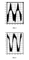
- FIG. 2 is a simulation depicting the fundamental power and second harmonic power where the output power ranges from about 24 dBm to about 30 dBm. Deep into compression the second harmonic power is as much as 17 dbm.
- FIG. 3 depicts the gate terminal voltage swinging from about ⁇ 3.1V to +0.7V.
- FIG. 4 depicts the output waveform swinging from about +0.3V to +17V. The output waveform depicted in FIG. 4 has a narrow bottom and wider top resulting in a second harmonic product which is difficult to filter.
- Waveforms that are symmetrical have no even order distortion as shown with the square wave in FIG. 5 .
- FIG. 6 shows the second harmonic level of the rectangular wave Vs duty cycle (d). As can be seen, if d can be kept to about 0.425 to 0.45, the second harmonic rejection can be ⁇ 10 db.
- FIG. 7 is a schematic diagram depicting a first illustrative embodiment of an amplifier circuit 700 of the invention.
- Circuit 700 comprises a power amplifier 710 , a negative clipping element 720 at the gate or base terminal of power amplifier 710 to control the duty cycle and even order harmonics at the power amplifier output, and a wide-band band pass filter (BPF) or a low pass filter (LPF) 740 to filter out the remaining harmonics.
- Circuit 700 also comprises a first DC blocking capacitor 750 at its input, a second DC blocking capacitor 760 at its output, and a load 770 .
- Amplifier 710 can be either a bipolar transistor or a field effect transistor, as shown, each having first, second and third terminals 712 , 714 , 716 .
- the first and second terminals are coupled to an emitter and a collector of the transistor; and the third terminal is coupled to a base of the transistor.
- the first and second terminals are coupled to source and drain regions of the transistor and the third terminal to a gate. In either case, a signal applied to the third terminal controls current flow between the first and second terminals.
- filter 740 is designed to have roughly the same impedance as the impedance of load 770 (within a ⁇ 10 db return loss).
- the negative clipping element 720 together with the output filter 740 provides a very wide-band amplifier of high output power with good harmonic rejection and low-loss. It is envisioned for instance, an amplifier using this invention could achieve adequate performance to cover EUTRAN bands (5,6,8,12,13,14,17,18,19,20,26) or EUTRAN bands (1,2,3,9,10,25,33,35,36,37,39) assuming each band is routed to an appropriate system filter to meet FCC (or similar) specifications.
- FIG. 9 depicts the gate terminal voltage swinging from about ⁇ 2.2 V to 1 V.
- FIG. 10 depicts the output waveform swinging from about 0 V to 20 V. As can be seen in FIG. 10 , the output waveform is symmetrical or nearly symmetrical.
- FIGS. 11 and 12 Further results of computer simulation are shown in FIGS. 11 and 12 .
- S Parameters are of a full amplifier with 37 db gain that covers a bandwidth of 1710 MHz-1980 MHz as depicted in FIG. 11 .
- the second harmonic distortion gives a rejection of >35 dbc.
- FIG. 13 depicts a second illustrative embodiment of a circuit 1300 of the invention that uses a voltage variable clipper element.
- Circuit 1300 comprises a power amplifier 1310 , a voltage variable clipping element 1320 at the gate or base terminal of power amplifier 1310 to control the duty cycle and even order harmonics at the power amplifier output, a voltage generator 1330 , and a wide-band band pass filter (BPF) or a low pass filter (LPF) 1340 to filter out the remaining harmonics.
- Circuit 1300 also comprises a first DC blocking capacitor 1350 at its input, a second DC blocking capacitor 1360 at its output, and a load 1370 .
- amplifier 1310 can be either a bipolar transistor or a field effect transistor, as shown, each having first, second and third terminals 1312 , 1314 , 1316 coupled to an emitter, collector and base of the bipolar transistor or to the source, drain and gate of the field effect transistor. In either case, a signal applied to the third terminal controls current flow between the first and second terminals.
- circuit 1300 The operation of circuit 1300 is similar to that of circuit 700 but the output of clipping element 1320 and therefore the second harmonic level is responsive to a control voltage supplied by voltage generator 1330 .
- the output of the voltage generator can be controlled so that it is responsive to a number of factors such as temperature, output power, oand/or VSWR under mismatch.
- the second order harmonic level can made to depend on such factors as temperature, output power, and VSWR under mismatch.
- the clipping voltage can be programmed; or the clipping voltage can be supplied by an adaptive feedback loop.
- the voltage variable clipper circuit can be made from any number of diodes, but in this case a GaAs Schottky diode is preferable.
- FIG. 14 depicts a diode 1410 in series with a variable voltage source 1420 such as an OP AMP and a capacitor 1430 to GND to make a low impedance voltage source to the negative clipping diode.
- Diode 1410 can be implemented in a variety of different forms such as a base-emitter, base collector, silicon PN junctions, germanium PN junctions, or JFET diode The resulting clipping voltage will be the built-in voltage plus/minus the voltage source voltage.
Landscapes
- Engineering & Computer Science (AREA)
- Power Engineering (AREA)
- Physics & Mathematics (AREA)
- Nonlinear Science (AREA)
- Amplifiers (AREA)
Abstract
The present invention breaks up the frequency bands which can be filtered by a simple low-loss band-pass or low pass filter. The second harmonic frequency is reduced by use of a non-linear clipper element which controls the driving waveform symmetry and can reduce the harmonics by as much as 5-15 db which makes the filter much simpler and allows the amplifier to remain wide-band. The output waveform from the amplifier is symmetrical or nearly symmetrical.
Description
This application is a continuation application of Non-Provisional application Ser. No. 14/276,400, filed May 13, 2014, which claims benefit of provisional application Ser. No. 61/824,047, filed May 16, 2013, the entire contents of which are incorporated herein by reference.
Wide-band amplifiers can reduce system costs and provide improved performance in many applications. Envelope tracking techniques can provide linear performance of wide-band amplifiers by running them deep into saturation. The improvement in efficiency is substantial with, for example, a 10%-20% improvement with LTE signals.
The problem for wide-band, envelope tracking amplifiers is that driving transistors deep into saturation produces substantial harmonics that can interfere with many receiving systems. While filter circuits can be used to reduce such harmonics, this results in reduced bandwidth and requires many discrete surface mount devices (SMDS). The additional filter circuits add power loss to the system and reduce the power amplifier efficiencies. A low pass, or band pass, filter can be used at the output of the amplifier to roll off the harmonics to acceptable levels. The hardest harmonic to filter is the second harmonic since it is the closest in frequency to the fundamental frequency. Typical power amplifier specifications require the second harmonic content to be 30-40 dbc.
The present invention breaks up the frequency bands that can be filtered by a simple low-loss band pass or low pass filter. The second harmonic frequency is reduced by use of a non-linear clipper element that controls the driving waveform and can reduce the harmonics by as much as 5-15 db which makes the filter much simpler and allows the amplifier to remain wide-band. The output waveform from the amplifier is symmetrical or nearly symmetrical.
These and other objects and advantages of the present invention will be apparent to those of ordinary skill in the art in view of the following detailed description in which:
Conventional silicon bipolar, HBT, JFET, MESFET and PHEMT devices suffer from the inherent problem that they have a diode element in their input controlling element such as the base or gate terminal. An illustrative prior art PHEMT circuit 100 is shown in FIG. 1 . Circuit 100 depicts a basic common source amplifier comprising a PHEMT transistor 110 having first, second, and third terminals 112, 114, 116, a first DC blocking capacitor 120 at the input of the circuit, a second DC blocking capacitor 130 at the output of the circuit, and a load 140. The PHEMT transistor has source and drain regions coupled to the first and second terminals 112 and 114 and a gate coupled to the third terminal 116.
When the RF input voltage swing becomes large enough to forward bias the gate diode, the input voltage is clamped to about 0.7 V and the excess voltage is stored across the first DC blocking capacitor 120. This forces the gate voltage to swing very far negative, such that the “ON” to “OFF duty cycle is not 50%.
Waveforms that are symmetrical have no even order distortion as shown with the square wave in FIG. 5 .
To make the system wide band, filter 740 is designed to have roughly the same impedance as the impedance of load 770 (within a ˜10 db return loss).
The negative clipping element 720 together with the output filter 740 provides a very wide-band amplifier of high output power with good harmonic rejection and low-loss. It is envisioned for instance, an amplifier using this invention could achieve adequate performance to cover EUTRAN bands (5,6,8,12,13,14,17,18,19,20,26) or EUTRAN bands (1,2,3,9,10,25,33,35,36,37,39) assuming each band is routed to an appropriate system filter to meet FCC (or similar) specifications.
Other applications of the wide-band amplifier of the present invention include its use in envelope tracking systems, in envelope elimination and restoration systems, and in polar modulation systems.
As shown in the plots of FIG. 8 , computer simulations of the circuit of FIG. 7 using two series PHEMT diodes (˜1.4V) show a second harmonic in deep saturation (>30 dbm) that reduces the signal power from ˜13 dbm to 17 dbm to −5 dbm to −4 dbm. FIG. 9 depicts the gate terminal voltage swinging from about −2.2 V to 1 V. FIG. 10 depicts the output waveform swinging from about 0 V to 20 V. As can be seen in FIG. 10 , the output waveform is symmetrical or nearly symmetrical.
Further results of computer simulation are shown in FIGS. 11 and 12 . S Parameters are of a full amplifier with 37 db gain that covers a bandwidth of 1710 MHz-1980 MHz as depicted in FIG. 11 . The second harmonic distortion gives a rejection of >35 dbc.
The operation of circuit 1300 is similar to that of circuit 700 but the output of clipping element 1320 and therefore the second harmonic level is responsive to a control voltage supplied by voltage generator 1330. The output of the voltage generator can be controlled so that it is responsive to a number of factors such as temperature, output power, oand/or VSWR under mismatch. Thus, the second order harmonic level can made to depend on such factors as temperature, output power, and VSWR under mismatch. The clipping voltage can be programmed; or the clipping voltage can be supplied by an adaptive feedback loop.
The voltage variable clipper circuit can be made from any number of diodes, but in this case a GaAs Schottky diode is preferable. FIG. 14 depicts a diode 1410 in series with a variable voltage source 1420 such as an OP AMP and a capacitor 1430 to GND to make a low impedance voltage source to the negative clipping diode. Diode 1410 can be implemented in a variety of different forms such as a base-emitter, base collector, silicon PN junctions, germanium PN junctions, or JFET diode The resulting clipping voltage will be the built-in voltage plus/minus the voltage source voltage.
As will be apparent to those skilled in the art, numerous variations may be practiced within the spirit and scope of the present invention.
Claims (18)
1. A wideband power amplifier circuit comprising:
a transistor configured as an amplifier stage of a power amplifier having first, second and third regions where a signal applied to the third region controls current flow between the first and second regions;
a waveform clipping element electrically coupled to the third region, which shapes a peak-to-peak amplitude of the signal applied to the third region, and which reduces a second harmonic of the signal, the waveform clipping element including a voltage variable clipper element controlled by a control voltage generated based at least in part on one or more of a temperature, an output power, or a voltage standing wave ratio under mismatch; and
a wideband filter electrically coupled to an output of the power amplifier to reduce harmonic levels of the signal.
2. The wideband power amplifier circuit of claim 1 wherein the waveform clipping element includes a negative waveform clipping element.
3. The wideband power amplifier circuit of claim 1 further comprising a voltage generator electrically coupled to the voltage variable clipper element, the voltage generator configured to generate the control voltage to control the operation of the voltage variable clipper element.
4. The wideband power amplifier circuit of claim 1 wherein the voltage variable clipper element includes one or more diodes.
5. The wideband power amplifier circuit of claim 4 wherein at least one of the diodes is a gallium-arsenide diode.
6. The wideband power amplifier circuit of claim 4 wherein at least one of the diodes is a Schottky diode.
7. The wideband power amplifier circuit of claim 1 wherein the voltage variable clipper element includes an operational amplifier and a capacitor.
8. The wideband power amplifier circuit of claim 1 wherein the transistor is a metal-oxide-semiconductor device in which the first region is a source region, the second region is a drain region, and the third region is a gate.
9. The wideband power amplifier circuit of claim 1 wherein the transistor is a bipolar device in which the first region is an emitter, the second region is a collector, and the third region is a base.
10. The wideband power amplifier circuit of claim 1 wherein the waveform clipping element reduces the second harmonic of the signal between 5 and 15 decibels.
11. The wideband power amplifier circuit of claim 1 wherein the wideband filter is configured to have substantially the same impedance as a load of the wideband power amplifier.
12. The wideband power amplifier circuit of claim 1 further comprising a first direct current blocking capacitor electrically coupled to the transistor.
13. The wideband power amplifier circuit of claim 1 further comprising a second direct current blocking capacitor electrically coupled to the wideband filter.
14. The wideband power amplifier circuit of claim 1 wherein the wideband filter is one of a band pass filter or a low pass filter.
15. The wideband power amplifier circuit of claim 1 wherein a clipping voltage of the waveform clipping element is determined based at least in part on an adaptive feedback loop.
16. The wideband power amplifier circuit of claim 1 wherein the waveform clipping element is a programmable waveform clipping element.
17. The wideband power amplifier circuit of claim 1 wherein the waveform clipping element is a nonlinear clipping element.
18. A communications system comprising:
a power amplifier including a transistor having first, second and third terminals where a signal applied to the third terminal controls current flow between the first and second terminals;
a waveform clipping circuit electrically coupled to the third terminal, which shapes a peak-to-peak amplitude of the signal applied to the third terminal, and which reduces a harmonic of the signal, the waveform clipping element including a voltage variable clipper element controlled by a control voltage generated based at least in part on one or more of a temperature, an output power, or a voltage standing wave ratio under mismatch; and
a filter electrically coupled to an output of the power amplifier to reduce harmonic levels of the signal.
Priority Applications (3)
| Application Number | Priority Date | Filing Date | Title |
|---|---|---|---|
| US15/413,146 US9935592B1 (en) | 2013-05-16 | 2017-01-23 | Wide-band amplifiers using clipper circuits for reduced harmonics |
| US15/928,639 US10230339B2 (en) | 2013-05-16 | 2018-03-22 | Wide-band amplifiers using clipper circuits for reduced harmonics |
| US16/297,225 US20190312557A1 (en) | 2013-05-16 | 2019-03-08 | Wide-band amplifiers using clipper circuits for reduced harmonics |
Applications Claiming Priority (3)
| Application Number | Priority Date | Filing Date | Title |
|---|---|---|---|
| US201361824047P | 2013-05-16 | 2013-05-16 | |
| US14/276,400 US9553551B1 (en) | 2013-05-16 | 2014-05-13 | Wide-band amplifiers using clipper circuits for reduced harmonics |
| US15/413,146 US9935592B1 (en) | 2013-05-16 | 2017-01-23 | Wide-band amplifiers using clipper circuits for reduced harmonics |
Related Parent Applications (1)
| Application Number | Title | Priority Date | Filing Date |
|---|---|---|---|
| US14/276,400 Continuation US9553551B1 (en) | 2013-05-16 | 2014-05-13 | Wide-band amplifiers using clipper circuits for reduced harmonics |
Related Child Applications (1)
| Application Number | Title | Priority Date | Filing Date |
|---|---|---|---|
| US15/928,639 Continuation US10230339B2 (en) | 2013-05-16 | 2018-03-22 | Wide-band amplifiers using clipper circuits for reduced harmonics |
Publications (1)
| Publication Number | Publication Date |
|---|---|
| US9935592B1 true US9935592B1 (en) | 2018-04-03 |
Family
ID=57795167
Family Applications (4)
| Application Number | Title | Priority Date | Filing Date |
|---|---|---|---|
| US14/276,400 Active 2034-10-14 US9553551B1 (en) | 2013-05-16 | 2014-05-13 | Wide-band amplifiers using clipper circuits for reduced harmonics |
| US15/413,146 Active US9935592B1 (en) | 2013-05-16 | 2017-01-23 | Wide-band amplifiers using clipper circuits for reduced harmonics |
| US15/928,639 Active US10230339B2 (en) | 2013-05-16 | 2018-03-22 | Wide-band amplifiers using clipper circuits for reduced harmonics |
| US16/297,225 Abandoned US20190312557A1 (en) | 2013-05-16 | 2019-03-08 | Wide-band amplifiers using clipper circuits for reduced harmonics |
Family Applications Before (1)
| Application Number | Title | Priority Date | Filing Date |
|---|---|---|---|
| US14/276,400 Active 2034-10-14 US9553551B1 (en) | 2013-05-16 | 2014-05-13 | Wide-band amplifiers using clipper circuits for reduced harmonics |
Family Applications After (2)
| Application Number | Title | Priority Date | Filing Date |
|---|---|---|---|
| US15/928,639 Active US10230339B2 (en) | 2013-05-16 | 2018-03-22 | Wide-band amplifiers using clipper circuits for reduced harmonics |
| US16/297,225 Abandoned US20190312557A1 (en) | 2013-05-16 | 2019-03-08 | Wide-band amplifiers using clipper circuits for reduced harmonics |
Country Status (1)
| Country | Link |
|---|---|
| US (4) | US9553551B1 (en) |
Families Citing this family (1)
| Publication number | Priority date | Publication date | Assignee | Title |
|---|---|---|---|---|
| US9553551B1 (en) | 2013-05-16 | 2017-01-24 | Skyworks Solutions, Inc. | Wide-band amplifiers using clipper circuits for reduced harmonics |
Citations (11)
| Publication number | Priority date | Publication date | Assignee | Title |
|---|---|---|---|---|
| US3585519A (en) | 1969-10-16 | 1971-06-15 | Us Navy | Narrow band intermediate frequency amplifier |
| US3863170A (en) | 1973-02-21 | 1975-01-28 | Bendix Corp | Thermally stable power amplifier |
| US5977823A (en) | 1997-09-11 | 1999-11-02 | Mitsubishi Denki Kabushiki Kaisha | Semiconductor amplifier circuit |
| US20040232983A1 (en) | 2003-05-21 | 2004-11-25 | The Boeing Company | Method and apparatus for low intermodulation distortion amplification in selected bands |
| US20090116663A1 (en) | 2007-11-05 | 2009-05-07 | Buuck David C | Combining an audio power amplifier and a power converter in a single device |
| US20100264992A1 (en) | 2009-04-20 | 2010-10-21 | Fujitsu Limited | Amplifying circuit and amplifying method |
| US20110181362A1 (en) | 2010-01-26 | 2011-07-28 | Yamaha Corporation | Signal processing circuit |
| US20130136278A1 (en) | 2011-11-29 | 2013-05-30 | Quilter Labs, LLC | Guitar amplifier |
| US20130241656A1 (en) | 2012-03-19 | 2013-09-19 | Auriga Measurement Systems, LLC | Power Amplification System Using Doherty Amplifier with Linearization Circuit and Related Techniques |
| US20140340155A1 (en) | 2013-03-15 | 2014-11-20 | Hbc Solutions, Inc. | Linearization of heterogeneous power amplifier systems |
| US9553551B1 (en) | 2013-05-16 | 2017-01-24 | Skyworks Solutions, Inc. | Wide-band amplifiers using clipper circuits for reduced harmonics |
Family Cites Families (8)
| Publication number | Priority date | Publication date | Assignee | Title |
|---|---|---|---|---|
| US4684876A (en) * | 1986-05-27 | 1987-08-04 | Creel Kirby B | Voltage regulating device using transistor means for voltage clipping and having load current compensation |
| US5430409A (en) * | 1994-06-30 | 1995-07-04 | Delco Electronics Corporation | Amplifier clipping distortion indicator with adjustable supply dependence |
| JPH09331542A (en) * | 1996-06-10 | 1997-12-22 | Matsushita Electric Ind Co Ltd | Primary color video signal output circuit, video receiver and television receiver |
| US6522194B1 (en) | 2000-12-29 | 2003-02-18 | Ericsson Inc. | Envelope restoration scheme for linear high-efficiency power amplification |
| US7286010B2 (en) * | 2006-01-26 | 2007-10-23 | D2Audio Corporation | Systems and methods for over-current protection |
| JP6263936B2 (en) | 2013-10-03 | 2018-01-24 | 富士通株式会社 | amplifier |
| US9356566B2 (en) | 2014-01-27 | 2016-05-31 | Harman International Industries, Inc. | Audio amplifier with an enhanced current limiter using a proxy signal |
| WO2016014634A1 (en) * | 2014-07-22 | 2016-01-28 | Healy michael g | Inductive distortion system and method |
-
2014
- 2014-05-13 US US14/276,400 patent/US9553551B1/en active Active
-
2017
- 2017-01-23 US US15/413,146 patent/US9935592B1/en active Active
-
2018
- 2018-03-22 US US15/928,639 patent/US10230339B2/en active Active
-
2019
- 2019-03-08 US US16/297,225 patent/US20190312557A1/en not_active Abandoned
Patent Citations (11)
| Publication number | Priority date | Publication date | Assignee | Title |
|---|---|---|---|---|
| US3585519A (en) | 1969-10-16 | 1971-06-15 | Us Navy | Narrow band intermediate frequency amplifier |
| US3863170A (en) | 1973-02-21 | 1975-01-28 | Bendix Corp | Thermally stable power amplifier |
| US5977823A (en) | 1997-09-11 | 1999-11-02 | Mitsubishi Denki Kabushiki Kaisha | Semiconductor amplifier circuit |
| US20040232983A1 (en) | 2003-05-21 | 2004-11-25 | The Boeing Company | Method and apparatus for low intermodulation distortion amplification in selected bands |
| US20090116663A1 (en) | 2007-11-05 | 2009-05-07 | Buuck David C | Combining an audio power amplifier and a power converter in a single device |
| US20100264992A1 (en) | 2009-04-20 | 2010-10-21 | Fujitsu Limited | Amplifying circuit and amplifying method |
| US20110181362A1 (en) | 2010-01-26 | 2011-07-28 | Yamaha Corporation | Signal processing circuit |
| US20130136278A1 (en) | 2011-11-29 | 2013-05-30 | Quilter Labs, LLC | Guitar amplifier |
| US20130241656A1 (en) | 2012-03-19 | 2013-09-19 | Auriga Measurement Systems, LLC | Power Amplification System Using Doherty Amplifier with Linearization Circuit and Related Techniques |
| US20140340155A1 (en) | 2013-03-15 | 2014-11-20 | Hbc Solutions, Inc. | Linearization of heterogeneous power amplifier systems |
| US9553551B1 (en) | 2013-05-16 | 2017-01-24 | Skyworks Solutions, Inc. | Wide-band amplifiers using clipper circuits for reduced harmonics |
Also Published As
| Publication number | Publication date |
|---|---|
| US10230339B2 (en) | 2019-03-12 |
| US9553551B1 (en) | 2017-01-24 |
| US20190312557A1 (en) | 2019-10-10 |
| US20180294780A1 (en) | 2018-10-11 |
Similar Documents
| Publication | Publication Date | Title |
|---|---|---|
| CN107508558B (en) | Power amplifying circuit | |
| Kim et al. | Optimization for envelope shaped operation of envelope tracking power amplifier | |
| US8350627B2 (en) | Hybrid class amplifier | |
| US9859844B1 (en) | Power amplifier circuit and method of design | |
| US10122327B2 (en) | Band-reconfigurable and load-adaptive power amplifier | |
| Moon et al. | A multimode/multiband envelope tracking transmitter with broadband saturated amplifier | |
| Gromorushkin et al. | Experimental Studies of the Envelope Elimination and Restoration HF Power Amplifier Characteristics with Broadband Unmatched Load | |
| US20150295542A1 (en) | Ultra wideband doherty amplifier | |
| US9917549B1 (en) | Dynamically configurable bias circuit for controlling gain expansion of multi-mode single chain linear power amplifiers | |
| US10673400B2 (en) | Gain stabilization for supply modulated RF and microwave integrated circuits | |
| KR102666474B1 (en) | RF power amplifier with frequency-selective impedance matching network | |
| Hallberg et al. | A class-J power amplifier with varactor-based dynamic load modulation across a large bandwidth | |
| Rahmani et al. | Novel Approach to Design of a Class-EJ Power Amplifier Using High Power Technology | |
| CN109586674B (en) | Power amplifying circuit | |
| US11894816B2 (en) | Power amplifier circuit | |
| US10027288B2 (en) | Amplifier | |
| US10230339B2 (en) | Wide-band amplifiers using clipper circuits for reduced harmonics | |
| US11114982B2 (en) | Power amplifier circuit | |
| Sarkeshi et al. | A novel Doherty amplifier for enhanced load modulation and higher bandwidth | |
| Kim et al. | Design of linear Doherty power amplifier for handset application | |
| Sajedin et al. | A Doherty power amplifier based on the harmonic generating mechanism | |
| Du et al. | Investigation of load modulated inverse class‐F power amplifier with extended conduction angle | |
| Mimis et al. | A reactively load-modulated RF low-power amplifier with multilevel supply voltage for multi-standard RF front-ends | |
| Amirpour et al. | Dynamic load modulated low-voltage GaN PA using novel low-loss GaN varactors | |
| US11211899B2 (en) | Power amplifying circuit |
Legal Events
| Date | Code | Title | Description |
|---|---|---|---|
| STCF | Information on status: patent grant |
Free format text: PATENTED CASE |
|
| MAFP | Maintenance fee payment |
Free format text: PAYMENT OF MAINTENANCE FEE, 4TH YEAR, LARGE ENTITY (ORIGINAL EVENT CODE: M1551); ENTITY STATUS OF PATENT OWNER: LARGE ENTITY Year of fee payment: 4 |
|
| MAFP | Maintenance fee payment |
Free format text: PAYMENT OF MAINTENANCE FEE, 8TH YEAR, LARGE ENTITY (ORIGINAL EVENT CODE: M1552); ENTITY STATUS OF PATENT OWNER: LARGE ENTITY Year of fee payment: 8 |