US9935271B2 - Organic electroluminescent device based on neutral free-radical electroluminescent material - Google Patents
Organic electroluminescent device based on neutral free-radical electroluminescent material Download PDFInfo
- Publication number
- US9935271B2 US9935271B2 US14/659,025 US201514659025A US9935271B2 US 9935271 B2 US9935271 B2 US 9935271B2 US 201514659025 A US201514659025 A US 201514659025A US 9935271 B2 US9935271 B2 US 9935271B2
- Authority
- US
- United States
- Prior art keywords
- organic electroluminescent
- electroluminescent device
- light
- layer
- transport layer
- Prior art date
- Legal status (The legal status is an assumption and is not a legal conclusion. Google has not performed a legal analysis and makes no representation as to the accuracy of the status listed.)
- Expired - Fee Related, expires
Links
- 0 *C1=CC(Cl)=C(CC2=C(Cl)C=C(Cl)C=C2Cl)C(Cl)=C1.C.[1*]C.[1*]C1=NC(Cl)=C(C(C2=C(Cl)C=C([2*])C=C2Cl)C2=C(Cl)C=C([3*])C=C2Cl)C(Cl)=N1.[2*]C1=CC(Cl)=C(C(C2=C(Cl)C=NC=C2Cl)C2=C(Cl)C=C([3*])C=C2Cl)C(Cl)=C1.[2*]C1=CC=C2C3=CC=C([3*])C=C3C(/C(C3=CC=CC=C3)=C3/C4=C(C=CC([2*])=C4)C4=C3/C=C([3*])\C=C/4)C2=C1 Chemical compound *C1=CC(Cl)=C(CC2=C(Cl)C=C(Cl)C=C2Cl)C(Cl)=C1.C.[1*]C.[1*]C1=NC(Cl)=C(C(C2=C(Cl)C=C([2*])C=C2Cl)C2=C(Cl)C=C([3*])C=C2Cl)C(Cl)=N1.[2*]C1=CC(Cl)=C(C(C2=C(Cl)C=NC=C2Cl)C2=C(Cl)C=C([3*])C=C2Cl)C(Cl)=C1.[2*]C1=CC=C2C3=CC=C([3*])C=C3C(/C(C3=CC=CC=C3)=C3/C4=C(C=CC([2*])=C4)C4=C3/C=C([3*])\C=C/4)C2=C1 0.000 description 11
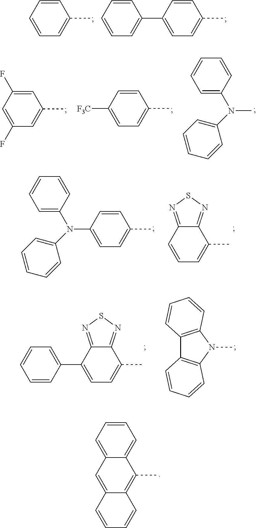
- YDHKTYKXFZKIND-UHFFFAOYSA-N CC1=C2C=CC=CC2=CC2=CC=CC=C21.CC1=CC(F)=CC(F)=C1.CC1=CC=C(C)C=C1.CC1=CC=C(C2=CC=CC=C2)C2=NSN=C12.CC1=CC=C(C2=CC=CC=C2)C=C1.CC1=CC=C(N(C2=CC=CC=C2)C2=CC=CC=C2)C=C1.CC1=CC=CC2=NSN=C12.CC1=CC=CC=C1.CN(C1=CC=CC=C1)C1=CC=CC=C1.CN1C2=C(C=CC=C2)C2=C1/C=C\C=C/2 Chemical compound CC1=C2C=CC=CC2=CC2=CC=CC=C21.CC1=CC(F)=CC(F)=C1.CC1=CC=C(C)C=C1.CC1=CC=C(C2=CC=CC=C2)C2=NSN=C12.CC1=CC=C(C2=CC=CC=C2)C=C1.CC1=CC=C(N(C2=CC=CC=C2)C2=CC=CC=C2)C=C1.CC1=CC=CC2=NSN=C12.CC1=CC=CC=C1.CN(C1=CC=CC=C1)C1=CC=CC=C1.CN1C2=C(C=CC=C2)C2=C1/C=C\C=C/2 YDHKTYKXFZKIND-UHFFFAOYSA-N 0.000 description 3
- NYUCSADKLMETQY-AXHYQYEMSA-N BCP.BN=P.C1=CC(N2C3=C(C=CC=C3)C3=C2C=CC=C3)=CC(N2C3=C(C=CC=C3)C3=C2C=CC=C3)=C1.C1=CC2=C(C=C1)N(C1=CC=C(C3=CC=C(N4C5=C(C=CC=C5)C5=C4/C=C\C=C/5)C=C3)C=C1)C1=C2C=CC=C1.C1=CC=C(N(C2=CC=C(C3=CC=C(N(C4=CC=CC=C4)C4=C5C=CC=CC5=CC=C4)C=C3)C=C2)C2=C3C=CC=CC3=CC=C2)C=C1.C1=CC=C(N2C(C3=CC(C4=NC5=C(C=CC=C5)N4C4=CC=CC=C4)=CC(C4=NC5=C(C=CC=C5)N4C4=CC=CC=C4)=C3)=NC3=C2C=CC=C3)C=C1.CC1=CC=CC(N(C2=CC=CC=C2)C2=CC=C(N(C3=CC=C(N(C4=CC=CC=C4)C4=CC=CC(C)=C4)C=C3)C3=CC=C(N(C4=CC=CC=C4)C4=CC=CC(C)=C4)C=C3)C=C2)=C1.[3H]P[BiH2] Chemical compound BCP.BN=P.C1=CC(N2C3=C(C=CC=C3)C3=C2C=CC=C3)=CC(N2C3=C(C=CC=C3)C3=C2C=CC=C3)=C1.C1=CC2=C(C=C1)N(C1=CC=C(C3=CC=C(N4C5=C(C=CC=C5)C5=C4/C=C\C=C/5)C=C3)C=C1)C1=C2C=CC=C1.C1=CC=C(N(C2=CC=C(C3=CC=C(N(C4=CC=CC=C4)C4=C5C=CC=CC5=CC=C4)C=C3)C=C2)C2=C3C=CC=CC3=CC=C2)C=C1.C1=CC=C(N2C(C3=CC(C4=NC5=C(C=CC=C5)N4C4=CC=CC=C4)=CC(C4=NC5=C(C=CC=C5)N4C4=CC=CC=C4)=C3)=NC3=C2C=CC=C3)C=C1.CC1=CC=CC(N(C2=CC=CC=C2)C2=CC=C(N(C3=CC=C(N(C4=CC=CC=C4)C4=CC=CC(C)=C4)C=C3)C3=CC=C(N(C4=CC=CC=C4)C4=CC=CC(C)=C4)C=C3)C=C2)=C1.[3H]P[BiH2] NYUCSADKLMETQY-AXHYQYEMSA-N 0.000 description 1
- XMZNAVKCKSWXCI-UHFFFAOYSA-M Br/C(C1=CC=CC=C1)=C1\C2=C(C=CC=C2)C2=C1/C=C\C=C/2.BrC(C1=CC=CC=C1)C1(Br)C2=C(C=CC=C2)C2=C1/C=C\C=C/2.CCO.O[Na] Chemical compound Br/C(C1=CC=CC=C1)=C1\C2=C(C=CC=C2)C2=C1/C=C\C=C/2.BrC(C1=CC=CC=C1)C1(Br)C2=C(C=CC=C2)C2=C1/C=C\C=C/2.CCO.O[Na] XMZNAVKCKSWXCI-UHFFFAOYSA-M 0.000 description 1
- DGJNXKRYTVOHRJ-UHFFFAOYSA-N Br/C(C1=CC=CC=C1)=C1\C2=C(C=CC=C2)C2=C1/C=C\C=C/2.C1=CC2=C(C=C1)C1=C(/C=C\C=C/1)C2.[H]C1(C(C2=CC=CC=C2)=C2C3=C(C=CC=C3)C3=C2C=CC=C3)C2=C(C=CC=C2)C2=C1C=CC=C2 Chemical compound Br/C(C1=CC=CC=C1)=C1\C2=C(C=CC=C2)C2=C1/C=C\C=C/2.C1=CC2=C(C=C1)C1=C(/C=C\C=C/1)C2.[H]C1(C(C2=CC=CC=C2)=C2C3=C(C=CC=C3)C3=C2C=CC=C3)C2=C(C=CC=C2)C2=C1C=CC=C2 DGJNXKRYTVOHRJ-UHFFFAOYSA-N 0.000 description 1
- YMIPMJVLFHOGGW-UHFFFAOYSA-N BrBr.BrC(C1=CC=CC=C1)C1(Br)C2=C(C=CC=C2)C2=C1/C=C\C=C/2.C1=CC=C(/C=C2/C3=C(C=CC=C3)C3=C2/C=C\C=C/3)C=C1.CC(=O)O Chemical compound BrBr.BrC(C1=CC=CC=C1)C1(Br)C2=C(C=CC=C2)C2=C1/C=C\C=C/2.C1=CC=C(/C=C2/C3=C(C=CC=C3)C3=C2/C=C\C=C/3)C=C1.CC(=O)O YMIPMJVLFHOGGW-UHFFFAOYSA-N 0.000 description 1
- IBRSRSPQTVMACA-MYJDPVRKSA-N C.C1=CC=C2C(=C1)NC1=C2/C=C\C=C/1.ClC1=CC(Cl)=C(C(C2=C(Cl)C=C(Cl)C=C2Cl)C2=C(Cl)C=C(Cl)C=C2Cl)C(Cl)=C1.ClC1=CC(Cl)=C(C(C2=C(Cl)C=C(Cl)C=C2Cl)C2=C(Cl)C=C(N3C4=CC=CC=C4C4=C3C=CC=C4)C=C2Cl)C(Cl)=C1.[3H][3H] Chemical compound C.C1=CC=C2C(=C1)NC1=C2/C=C\C=C/1.ClC1=CC(Cl)=C(C(C2=C(Cl)C=C(Cl)C=C2Cl)C2=C(Cl)C=C(Cl)C=C2Cl)C(Cl)=C1.ClC1=CC(Cl)=C(C(C2=C(Cl)C=C(Cl)C=C2Cl)C2=C(Cl)C=C(N3C4=CC=CC=C4C4=C3C=CC=C4)C=C2Cl)C(Cl)=C1.[3H][3H] IBRSRSPQTVMACA-MYJDPVRKSA-N 0.000 description 1
- UUHCRSLVKOSFGG-RQOUITMFSA-N C.ClC1=CC(Cl)=C(C(C2=C(Cl)C=C(Cl)C=C2Cl)C2=C(Cl)C=C(Cl)C=C2Cl)C(Cl)=C1.ClC1=CC(Cl)=C(C(C2=C(Cl)C=C(Cl)C=C2Cl)C2=C(Cl)C=C(Cl)C=C2Cl)C(Cl)=C1.[3H][3H] Chemical compound C.ClC1=CC(Cl)=C(C(C2=C(Cl)C=C(Cl)C=C2Cl)C2=C(Cl)C=C(Cl)C=C2Cl)C(Cl)=C1.ClC1=CC(Cl)=C(C(C2=C(Cl)C=C(Cl)C=C2Cl)C2=C(Cl)C=C(Cl)C=C2Cl)C(Cl)=C1.[3H][3H] UUHCRSLVKOSFGG-RQOUITMFSA-N 0.000 description 1
- KRHIUOPNJDLWGU-UHFFFAOYSA-M C1=CC2=C(C=C1)C1=C(/C=C\C=C/1)C2.C1=CC=C(/C=C2/C3=C(C=CC=C3)C3=C2/C=C\C=C/3)C=C1.O=CC1=CC=CC=C1.O[K] Chemical compound C1=CC2=C(C=C1)C1=C(/C=C\C=C/1)C2.C1=CC=C(/C=C2/C3=C(C=CC=C3)C3=C2/C=C\C=C/3)C=C1.O=CC1=CC=CC=C1.O[K] KRHIUOPNJDLWGU-UHFFFAOYSA-M 0.000 description 1
- XKESVVSGJMGQDC-UHFFFAOYSA-N C1=CC=C(C(=C2C3=C(C=CC=C3)C3=C2C=CC=C3)C2C3=C(C=CC=C3)C3=C2C=CC=C3)C=C1.O=[N+]([O-])O[Ag].[H]C1(C(C2=CC=CC=C2)=C2C3=C(C=CC=C3)C3=C2C=CC=C3)C2=C(C=CC=C2)C2=C1C=CC=C2 Chemical compound C1=CC=C(C(=C2C3=C(C=CC=C3)C3=C2C=CC=C3)C2C3=C(C=CC=C3)C3=C2C=CC=C3)C=C1.O=[N+]([O-])O[Ag].[H]C1(C(C2=CC=CC=C2)=C2C3=C(C=CC=C3)C3=C2C=CC=C3)C2=C(C=CC=C2)C2=C1C=CC=C2 XKESVVSGJMGQDC-UHFFFAOYSA-N 0.000 description 1
- RVSOLZGZSMANIF-UHFFFAOYSA-N C1=CC=C2C(=C1)NC1=C2/C=C\C=C/1.ClC1=CC(Cl)=C(C(C2=C(Cl)C=NC=C2Cl)C2=C(Cl)C=C(Cl)C=C2Cl)C(Cl)=C1.ClC1=CC(Cl)=C(C(C2=C(Cl)C=NC=C2Cl)C2=C(Cl)C=C(N3C4=CC=CC=C4C4=C3C=CC=C4)C=C2Cl)C(Cl)=C1 Chemical compound C1=CC=C2C(=C1)NC1=C2/C=C\C=C/1.ClC1=CC(Cl)=C(C(C2=C(Cl)C=NC=C2Cl)C2=C(Cl)C=C(Cl)C=C2Cl)C(Cl)=C1.ClC1=CC(Cl)=C(C(C2=C(Cl)C=NC=C2Cl)C2=C(Cl)C=C(N3C4=CC=CC=C4C4=C3C=CC=C4)C=C2Cl)C(Cl)=C1 RVSOLZGZSMANIF-UHFFFAOYSA-N 0.000 description 1
- IROFMPWKPZCTGK-UHFFFAOYSA-K ClC(Cl)Cl.ClC1=CC(Cl)=C(C(C2=C(Cl)C=C(Cl)C=C2Cl)C2=C(Cl)C=C(Cl)C=C2Cl)C(Cl)=C1.ClC1=CC(Cl)=CC(Cl)=C1.Cl[Al](Cl)Cl Chemical compound ClC(Cl)Cl.ClC1=CC(Cl)=C(C(C2=C(Cl)C=C(Cl)C=C2Cl)C2=C(Cl)C=C(Cl)C=C2Cl)C(Cl)=C1.ClC1=CC(Cl)=CC(Cl)=C1.Cl[Al](Cl)Cl IROFMPWKPZCTGK-UHFFFAOYSA-K 0.000 description 1
- ZNXWMZCHEMDSIT-GHTNUIMXSA-N ClC1=CC(Cl)=C(C(C2=C(Cl)C=C(Cl)C=C2Cl)C2=C(Cl)N=C(Cl)N=C2Cl)C(Cl)=C1.ClC1=CC(Cl)=C(C(C2=C(Cl)C=C(Cl)C=C2Cl)C2=C(Cl)N=C(Cl)N=C2Cl)C(Cl)=C1.[3H]B(C)[Pm] Chemical compound ClC1=CC(Cl)=C(C(C2=C(Cl)C=C(Cl)C=C2Cl)C2=C(Cl)N=C(Cl)N=C2Cl)C(Cl)=C1.ClC1=CC(Cl)=C(C(C2=C(Cl)C=C(Cl)C=C2Cl)C2=C(Cl)N=C(Cl)N=C2Cl)C(Cl)=C1.[3H]B(C)[Pm] ZNXWMZCHEMDSIT-GHTNUIMXSA-N 0.000 description 1
- RSLHJYYQBDZDCU-UHFFFAOYSA-N ClC1=CC(Cl)=C(C(C2=C(Cl)C=C(Cl)C=C2Cl)C2=C(Cl)N=C(Cl)N=C2Cl)C(Cl)=C1.ClC1=CC(Cl)=CC(Cl)=C1.O=CC1=C(Cl)N=C(Cl)N=C1Cl Chemical compound ClC1=CC(Cl)=C(C(C2=C(Cl)C=C(Cl)C=C2Cl)C2=C(Cl)N=C(Cl)N=C2Cl)C(Cl)=C1.ClC1=CC(Cl)=CC(Cl)=C1.O=CC1=C(Cl)N=C(Cl)N=C1Cl RSLHJYYQBDZDCU-UHFFFAOYSA-N 0.000 description 1
- VPZFSPJAJAJOLF-UHFFFAOYSA-N ClC1=CC(Cl)=C(C(C2=C(Cl)C=NC=C2Cl)C2=C(Cl)C=C(Cl)C=C2Cl)C(Cl)=C1.ClC1=CC(Cl)=C(C(C2=C(Cl)C=NC=C2Cl)C2=C(Cl)C=C(Cl)C=C2Cl)C(Cl)=C1 Chemical compound ClC1=CC(Cl)=C(C(C2=C(Cl)C=NC=C2Cl)C2=C(Cl)C=C(Cl)C=C2Cl)C(Cl)=C1.ClC1=CC(Cl)=C(C(C2=C(Cl)C=NC=C2Cl)C2=C(Cl)C=C(Cl)C=C2Cl)C(Cl)=C1 VPZFSPJAJAJOLF-UHFFFAOYSA-N 0.000 description 1
- FECVUDLDXDTNBO-UHFFFAOYSA-N ClC1=CC(Cl)=C(C(C2=C(Cl)C=NC=C2Cl)C2=C(Cl)C=C(Cl)C=C2Cl)C(Cl)=C1.ClC1=CC(Cl)=CC(Cl)=C1.O=CC1=C(Cl)C=NC=C1Cl Chemical compound ClC1=CC(Cl)=C(C(C2=C(Cl)C=NC=C2Cl)C2=C(Cl)C=C(Cl)C=C2Cl)C(Cl)=C1.ClC1=CC(Cl)=CC(Cl)=C1.O=CC1=C(Cl)C=NC=C1Cl FECVUDLDXDTNBO-UHFFFAOYSA-N 0.000 description 1
- NNDIQJVRXGHGCX-UHFFFAOYSA-N ClC1=CN=CC(Cl)=C1.O=CC1=C(Cl)C=NC=C1Cl Chemical compound ClC1=CN=CC(Cl)=C1.O=CC1=C(Cl)C=NC=C1Cl NNDIQJVRXGHGCX-UHFFFAOYSA-N 0.000 description 1
- CMRNLJXTIUHKLD-UHFFFAOYSA-N N#CC1=CC=C(/C(=C2\C3=C(C=CC=C3)C3=C2/C=C\C=C/3)C2C3=CC=CC=C3C3=CC=CC=C32)C=C1 Chemical compound N#CC1=CC=C(/C(=C2\C3=C(C=CC=C3)C3=C2/C=C\C=C/3)C2C3=CC=CC=C3C3=CC=CC=C32)C=C1 CMRNLJXTIUHKLD-UHFFFAOYSA-N 0.000 description 1
- SSEDHLBEAYBBHY-XZVVQQHRSA-N O=C1CC(=O)NC(=O)N1.O=CC1=C(Cl)N=C(Cl)N=C1Cl.O=P(Cl)(Cl)Cl.[2H]CF Chemical compound O=C1CC(=O)NC(=O)N1.O=CC1=C(Cl)N=C(Cl)N=C1Cl.O=P(Cl)(Cl)Cl.[2H]CF SSEDHLBEAYBBHY-XZVVQQHRSA-N 0.000 description 1
- KFKKPHMVLMMNKE-LVCRGMNSSA-N O=P(C1=CC=CC=C1)(C1=CC=CC=C1)C1=CC=CC(C2=NC(C3=CC(P(=O)(C4=CC=CC=C4)C4=CC=CC=C4)=CC=C3)=NC(C3=CC(P(=O)(C4=CC=CC=C4)C4=CC=CC=C4)=CC=C3)=N2)=C1.[3H]P([3H])([3H])=O Chemical compound O=P(C1=CC=CC=C1)(C1=CC=CC=C1)C1=CC=CC(C2=NC(C3=CC(P(=O)(C4=CC=CC=C4)C4=CC=CC=C4)=CC=C3)=NC(C3=CC(P(=O)(C4=CC=CC=C4)C4=CC=CC=C4)=CC=C3)=N2)=C1.[3H]P([3H])([3H])=O KFKKPHMVLMMNKE-LVCRGMNSSA-N 0.000 description 1
Images


Classifications
-
- H—ELECTRICITY
- H10—SEMICONDUCTOR DEVICES; ELECTRIC SOLID-STATE DEVICES NOT OTHERWISE PROVIDED FOR
- H10K—ORGANIC ELECTRIC SOLID-STATE DEVICES
- H10K85/00—Organic materials used in the body or electrodes of devices covered by this subclass
- H10K85/60—Organic compounds having low molecular weight
- H10K85/615—Polycyclic condensed aromatic hydrocarbons, e.g. anthracene
- H10K85/626—Polycyclic condensed aromatic hydrocarbons, e.g. anthracene containing more than one polycyclic condensed aromatic rings, e.g. bis-anthracene
-
- H01L51/0058—
-
- H01L51/0052—
-
- H01L51/0067—
-
- H01L51/0072—
-
- H01L51/5012—
-
- H—ELECTRICITY
- H10—SEMICONDUCTOR DEVICES; ELECTRIC SOLID-STATE DEVICES NOT OTHERWISE PROVIDED FOR
- H10K—ORGANIC ELECTRIC SOLID-STATE DEVICES
- H10K50/00—Organic light-emitting devices
- H10K50/10—OLEDs or polymer light-emitting diodes [PLED]
- H10K50/11—OLEDs or polymer light-emitting diodes [PLED] characterised by the electroluminescent [EL] layers
-
- H—ELECTRICITY
- H10—SEMICONDUCTOR DEVICES; ELECTRIC SOLID-STATE DEVICES NOT OTHERWISE PROVIDED FOR
- H10K—ORGANIC ELECTRIC SOLID-STATE DEVICES
- H10K85/00—Organic materials used in the body or electrodes of devices covered by this subclass
- H10K85/60—Organic compounds having low molecular weight
- H10K85/615—Polycyclic condensed aromatic hydrocarbons, e.g. anthracene
-
- H—ELECTRICITY
- H10—SEMICONDUCTOR DEVICES; ELECTRIC SOLID-STATE DEVICES NOT OTHERWISE PROVIDED FOR
- H10K—ORGANIC ELECTRIC SOLID-STATE DEVICES
- H10K85/00—Organic materials used in the body or electrodes of devices covered by this subclass
- H10K85/60—Organic compounds having low molecular weight
- H10K85/649—Aromatic compounds comprising a hetero atom
- H10K85/654—Aromatic compounds comprising a hetero atom comprising only nitrogen as heteroatom
-
- H—ELECTRICITY
- H10—SEMICONDUCTOR DEVICES; ELECTRIC SOLID-STATE DEVICES NOT OTHERWISE PROVIDED FOR
- H10K—ORGANIC ELECTRIC SOLID-STATE DEVICES
- H10K85/00—Organic materials used in the body or electrodes of devices covered by this subclass
- H10K85/60—Organic compounds having low molecular weight
- H10K85/649—Aromatic compounds comprising a hetero atom
- H10K85/657—Polycyclic condensed heteroaromatic hydrocarbons
- H10K85/6572—Polycyclic condensed heteroaromatic hydrocarbons comprising only nitrogen in the heteroaromatic polycondensed ring system, e.g. phenanthroline or carbazole
-
- C—CHEMISTRY; METALLURGY
- C09—DYES; PAINTS; POLISHES; NATURAL RESINS; ADHESIVES; COMPOSITIONS NOT OTHERWISE PROVIDED FOR; APPLICATIONS OF MATERIALS NOT OTHERWISE PROVIDED FOR
- C09K—MATERIALS FOR MISCELLANEOUS APPLICATIONS, NOT PROVIDED FOR ELSEWHERE
- C09K2211/00—Chemical nature of organic luminescent or tenebrescent compounds
- C09K2211/10—Non-macromolecular compounds
- C09K2211/1003—Carbocyclic compounds
- C09K2211/1007—Non-condensed systems
-
- C—CHEMISTRY; METALLURGY
- C09—DYES; PAINTS; POLISHES; NATURAL RESINS; ADHESIVES; COMPOSITIONS NOT OTHERWISE PROVIDED FOR; APPLICATIONS OF MATERIALS NOT OTHERWISE PROVIDED FOR
- C09K—MATERIALS FOR MISCELLANEOUS APPLICATIONS, NOT PROVIDED FOR ELSEWHERE
- C09K2211/00—Chemical nature of organic luminescent or tenebrescent compounds
- C09K2211/10—Non-macromolecular compounds
- C09K2211/1003—Carbocyclic compounds
- C09K2211/1011—Condensed systems
-
- C—CHEMISTRY; METALLURGY
- C09—DYES; PAINTS; POLISHES; NATURAL RESINS; ADHESIVES; COMPOSITIONS NOT OTHERWISE PROVIDED FOR; APPLICATIONS OF MATERIALS NOT OTHERWISE PROVIDED FOR
- C09K—MATERIALS FOR MISCELLANEOUS APPLICATIONS, NOT PROVIDED FOR ELSEWHERE
- C09K2211/00—Chemical nature of organic luminescent or tenebrescent compounds
- C09K2211/10—Non-macromolecular compounds
- C09K2211/1018—Heterocyclic compounds
- C09K2211/1025—Heterocyclic compounds characterised by ligands
- C09K2211/1044—Heterocyclic compounds characterised by ligands containing two nitrogen atoms as heteroatoms
- C09K2211/1051—Heterocyclic compounds characterised by ligands containing two nitrogen atoms as heteroatoms with sulfur
-
- H01L2251/303—
-
- H01L2251/308—
-
- H01L51/0081—
-
- H01L51/5016—
-
- H—ELECTRICITY
- H10—SEMICONDUCTOR DEVICES; ELECTRIC SOLID-STATE DEVICES NOT OTHERWISE PROVIDED FOR
- H10K—ORGANIC ELECTRIC SOLID-STATE DEVICES
- H10K2101/00—Properties of the organic materials covered by group H10K85/00
- H10K2101/10—Triplet emission
-
- H—ELECTRICITY
- H10—SEMICONDUCTOR DEVICES; ELECTRIC SOLID-STATE DEVICES NOT OTHERWISE PROVIDED FOR
- H10K—ORGANIC ELECTRIC SOLID-STATE DEVICES
- H10K2102/00—Constructional details relating to the organic devices covered by this subclass
-
- H—ELECTRICITY
- H10—SEMICONDUCTOR DEVICES; ELECTRIC SOLID-STATE DEVICES NOT OTHERWISE PROVIDED FOR
- H10K—ORGANIC ELECTRIC SOLID-STATE DEVICES
- H10K2102/00—Constructional details relating to the organic devices covered by this subclass
- H10K2102/10—Transparent electrodes, e.g. using graphene
- H10K2102/101—Transparent electrodes, e.g. using graphene comprising transparent conductive oxides [TCO]
- H10K2102/103—Transparent electrodes, e.g. using graphene comprising transparent conductive oxides [TCO] comprising indium oxides, e.g. ITO
-
- H—ELECTRICITY
- H10—SEMICONDUCTOR DEVICES; ELECTRIC SOLID-STATE DEVICES NOT OTHERWISE PROVIDED FOR
- H10K—ORGANIC ELECTRIC SOLID-STATE DEVICES
- H10K85/00—Organic materials used in the body or electrodes of devices covered by this subclass
- H10K85/30—Coordination compounds
- H10K85/321—Metal complexes comprising a group IIIA element, e.g. Tris (8-hydroxyquinoline) gallium [Gaq3]
- H10K85/324—Metal complexes comprising a group IIIA element, e.g. Tris (8-hydroxyquinoline) gallium [Gaq3] comprising aluminium, e.g. Alq3
Definitions
- the invention relates to an organic electroluminescent device, and in particular an organic electroluminescent device using a neutral free-radical electroluminescent material as a light-emitting layer.
- the organic electroluminescent device exhibits a bright application prospect in the display and illumination fields since it has the advantages, such as a simple manufacturing process, a wide range of materials, a controllable structure, being super-thin and flexible, etc.
- Some organic electroluminescent devices industrially applicable or close to industrially applicable have appeared, for example, display screens based on an active matrix organic electroluminescent diode from the Samsung company have been widely used in Galaxy series mobile phones and the large size televisions thereof also have appeared on the market.
- the organic white-light illumination technology also has been developing towards the target of low-cost, high-efficiency, and long-life flat-panel light sources.
- the resulting ratio of the singlet excitions to the triplet excitions is 1:3; for an organic fluorescent material, the transition of a triplet excition to the ground state is forbidden, there is only luminescence from the transition of a singlet excition to the ground state; therefore the internal quantum efficiency of the device has an upper limit of 25%.
- organic fluorescent electroluminescent devices i.e., a device in which an organic phosphorescent material is used for luminescence, U.S. Pat. No. 6,303,238; M. A. Baldo, et al., Nature 395, 151, (1998); Y. G. Ma, et al., Synth. Met. 94, 245, (1998)).
- organic light-emitting materials i.e., the organic phosphorescent materials
- the organic light-emitting materials i.e., the organic phosphorescent materials
- the transition of a triplet excition to the ground state becomes possible by the strong spin-orbital coupling of the heavy metal atom.
- the internal quantum efficiency can reach 100%.
- the current high-efficiency organic phosphorescent materials are all expensive rare metal coordination complexes, resulting significant increase of the production costs of organic phosphorescent electroluminescent devices.
- the organic florescent electroluminescent devices the light emission of the singlet excitions are used (the upper limit of the internal quantum efficiency is only 25%); in the organic phosphorescent electroluminescent device, the light emission of the triplet excitions are used (the organic phosphorescent light-emitting materials are expensive); they have disadvantages of their own; therefore it is a trend to develop an organic electroluminescent device which can reach an upper limit of internal quantum efficiency of 100% without using expensive rare metals. So far there is no report on an organic electroluminescent device using a neutral free-radical electroluminescent material as a light-emitting layer.
- An object of the present invention is to provide an organic electroluminescent device, which emits light on the basis of the transition of a doublet electron between different orbits of organic neutral free-radical electroluminescent materials, can replace an organic phosphorescent electroluminescent device.
- the device based on organic neutral free-radical electroluminescent materials has relatively low costs and has an internal quantum efficiency upper limit of 100%.
- the neutral free-radical electroluminescent materials described in the present invention are classified into the following four classes: 1,3-bis(diphenylene)-2-phenylallyl free radicals and derivatives thereof; tri(2,4,6-trichlorophenyl)methyl free radicals and derivatives thereof; 3,5-dichloro-4-pyridyl)bis(2,4,6-trichlorophenyl)methyl free radicals and derivatives thereof; (2,4,6-trichloro-5-pyrimidinyl)bis(2,4,6-trichlorophenyl)methyl free radicals and derivatives thereof, and have the following general structures:
- R, R 1 , R 2 and R 3 are the same or different
- R, R 1 , R 2 , R 3 ⁇ H, F, Cl, CN . . .
- R, R 1 , R 2 and R 3 are selected from an aromatic amine, heterocyclic aromatic hydrocarbon or fused ring aromatic hydrocarbon compound or an atom, a group as shown in the above formulas or a derivative from any combination thereof.
- the above-mentioned neutral free-radical electroluminescent material can be made as a light-emitting layer of the device by evaporation, etc.
- the spin quantum number of one electron is 1 ⁇ 2, corresponding to a doublet state.
- the light emission of the organic electroluminescent device in the present invention is from the transition of the doublet electron of the organic neutral free-radical molecules from a higher level molecular orbit to a lower level singly occupied molecular orbit (SOMO), which is different from the emission from a singlet excition or a triplet excition;
- SOMO singly occupied molecular orbit
- FIG. 1 an electroluminescence spectrum of a device at a voltage of 6 V, characterizing the luminescence spectrum of the device from example 5;
- FIG. 2 voltage-current density and voltage-luminance curves of a device, characterizing the voltage-current density and voltage-luminance of the device from example 5;
- FIG. 3 an electroluminescence spectrum of a device at a voltage of 7 V, characterizing the luminescence spectrum of the device from example 6;
- FIG. 4 voltage-current density and voltage-luminance curves of a device, characterizing the voltage-current density and voltage-luminance of the device from example 6;
- FIG. 5 an electroluminescence spectrum of a device at a voltage of 9 V, characterizing the luminescence spectrum of the device from example 7;
- FIG. 6 voltage-current density and voltage-luminance curves of a device, characterizing the voltage-current density and voltage-luminance of the device from example 7.
- Step 1 Preparation of 2,7-disubstituted-9-(substituted benzylidene)-9H-fluorene
- Step 2 Preparation of 2,7-disubstituted-9-bromo-9-[bromo-(substituted benzylidene)]-9H-Fluorene
- Step 3 Preparation of 2,7-disubstituted-9-[-bromo-(substituted phenyl)methylene]-9H-fluorene
- Step 4 Preparation of ((2,7-disubstituted-9H-fluorene-9-vinylidene)-2,7-disubstituted (9H-fluorene-9-yl)methylene)substituted benzene
- Step 5 Preparation of ((2,7-disubstituted-9H-fluorene-9-vinylidene)-2,7-disubstituted (9H-fluorene-9-yl)methylene)substituted phenyl free radical
- TTM tri(2,4,6-trichlorophenyl)methyl free radical
- the excessive I 2 was washed with a 10% Na 2 S 2 O 3 solution three times; the water layer was extracted with ethyl ether several times, dried over anhydrous MgSO 4 ; the solvent was evaporated.
- the mixture was purified by Al2O3 column chromatography.
- the basic structure of an organic electroluminescent device comprises a substrate, a pair of electrode (an anode and a cathode) and an organic light-emitting layer between this pair of electrodes; the device further comprises a hole transport layer disposed between the light-emitting layer and the anode; (generally an aromatic amine derivative, such as N,N′-diphenyl-N,N′-(1-naphthyl)-1,1′-biphenyl-4,4′-diamine (abbreviation, NPB), 4,4′,4′′-Tris(3-methylphenylphenylamino)triphenylamine (abbreviation, m-MTDATA), etc.); an electron transport layer disposed between the light emitting layer and the cathode (generally consisting of electron-withdrawing groups, such as 1,3,5-tri(1-phenyl-1-hydrogen-benzimidazole-2-yl)benzene (TPBi)).
- NPB aromatic
- the substrate is a transparent base body;
- the first electrode layer (anode layer) can be an inorganic material or an organic conductive polymer, wherein the inorganic material is generally a metal oxide, such as ITO, zinc oxide, tin zinc oxide, etc., or a metal having a relatively high work function, such as gold, copper, silver, etc., most preferably is selected from ITO, and the organic conductive polymer is a material of one of poly thiophene/sodium polyvinyl benzene sulfonate (abbreviation, PEDOT PSS), polyaniline (abbreviation, PANI);
- the second electrode layer (cathode layer) is generally a metal having a low work function or an alloy thereof with gold, silver, or a metal fluoride; in the present invention, the cathode layer is preferably LiF/Al.
- the light-emitting layer consists of a compound of a general formula in the present invention or a compound of a general formula in the present invention doped into a matrix material.
- the matrix material in the present invention is 4,4′-di(9-carbazole)biphenyl (abbreviation, CBP) or 1,3′-di(9-carbazole)benzene (abbreviation, mCP) and the doping mass concentration range is 0.1%-50%.
- the above device structure also can comprise a hole injection layer located between the anode and the hole transport layer, wherein the hole injection layer generally is a metal oxide, such as molybdenum trioxide (MoO 3 ); an electron injection layer disposed between the electron transport layer and the cathode, wherein the electron injection layer material is typically such as lithium fluoride (LiF), fluorine cesium (CsF), cesium carbonate (Cs 2 CO 3 ); a hole blocking layer located between the electron transport layer and the light-emitting layer, for example, 2,9-dimethyl-4,7-biphenyl-1,10-o-phenanthroline (abbreviation BCP); an electron blocking layer located between the hole transporting layer and the light-emitting layer, such as 4,4′,4′′-tri(carbazole-9-yl)triphenylamine (abbreviation TCTA), 4,4′-cyclohexyl[N,N-bis(4-methylphenyl)phenylamine (abb
- the device of the present invention is manufactured as follows:
- the organic electroluminescent device is prepared by a multi-source organic molecule vapor deposition system, wherein the degree of vacuum of the system can reach 1 ⁇ 10 ⁇ 4 Pa.
- the materials to be evaporated are charged in quartz crucibles, wherein the temperature of each crucible can be controlled independently, and the control accuracy is 0.1° C.
- the substrate is placed in the upper part of the vacuum chamber with a distance of 20 cm from the evaporation source.
- the substrate is treated by the following procedures: the substrate is rinsed with toluene, acetone, ethanol, and deionized water and ultrasonic-cleaned, and then treated by ultraviolet light radiation.
- the evaporation materials used are placed into different quartz crucibles in the organic molecule vapor deposition system, respectively, and grow the organic materials of different contents and thicknesses according to the designed structure, and during the growing, the degree of vacuum of the system is maintained at about 3 ⁇ 10 ⁇ 4 Pa.
- the growth thickness and rate are monitored by a thickness gauge.
- Example 5 Organic Electroluminescent Device Based on 1,3-bisdiphenylene-2-phenylallyl Free Radical (Abbreviation BDPA)
- the device has the following structure: ITO/MoO 3 (5 nm)/mCP(10 nm)/BDPA:Alq 3 (wt. 10%, 50 nm)/Alq 3 (10 nm)/LiF(0.8 nm)/Al.
- FIG. 1 The electroluminescence spectrum of the device at 6 V is as shown in FIG. 1 , the peak wavelength is at 572 nm, and is the emission of BDPA.
- FIG. 2 is voltage-current density and voltage-luminance curves of the device.
- Example 6 Organic Electroluminescent Device Based on a tri(2,4,6-trichlorophenyl)methyl Free Radical Derivative
- NPB is used as the hole transport layer
- TPBi is used as the electron transport layer
- CBP doped with [4-(N-carbazolyl)-2,6-dichlorophenyl]bis(2,4,6-trichlorophenyl)-methyl free radical (abbriviation, TTM-1Cz) is used as the light-emitting layer
- the structure is: ITO/NPB (30 nm)/TTM-1Cz: CBP (wt. 5%; 40 nm)/TPBI (35 nm)/LiF (0.8 nm)/Al (100 nm).
- the electroluminescence spectrum of the device at 7 V is as shown in FIG. 3 , the peak wavelength is at 694 nm, and is the emission of TTM-1Cz.
- FIG. 4 is voltage-current density and voltage-luminance curves of the device.
- Example 7 Organic Electroluminescent Device Based on (3,5-dichloro-4-pyridinyl)bis(2,4,6-trichlorophenyl)methyl Free Radical
- mCP is used as the hole transport layer
- PO-T2T is used as the electron transport layer
- PO-T2T doped with (3,5-dichloro-4-pyridinyl)bis(2,4,6-trichlorophenyl)methyl free radical (abbreviation, PyBTM) is used as the light-emitting layer
- the structure is: ITO/MoO3(6 nm)/mCP(10 nm)/PyBTM:PO-T2T(wt. 7%, 25 nm)/PO-T2T(30 nm)/LiF(0.8n m)/Al(100 nmn).
- the electroluminescence spectrum of the device at 9 V is as shown in FIG. 5 , the peak wavelength is at 694 nm, and is the emission of PyBTM.
- FIG. 6 is voltage-current density and voltage-luminance curves of the device.
Landscapes
- Physics & Mathematics (AREA)
- Chemical & Material Sciences (AREA)
- Spectroscopy & Molecular Physics (AREA)
- Engineering & Computer Science (AREA)
- Materials Engineering (AREA)
- Optics & Photonics (AREA)
- Organic Chemistry (AREA)
- Electroluminescent Light Sources (AREA)
Abstract
Description


Claims (16)


Applications Claiming Priority (6)
| Application Number | Priority Date | Filing Date | Title |
|---|---|---|---|
| CN201410018393.9 | 2014-01-15 | ||
| CN201410018393.9A CN103715361B (en) | 2014-01-15 | 2014-01-15 | A kind of based on the organic electroluminescence device of doublet electronics at the different interorbital transition luminescence of Neutral radical molecule |
| CN201410018393 | 2014-01-15 | ||
| CN201410639989 | 2014-11-11 | ||
| CN201410639989.0A CN104449671B (en) | 2014-11-11 | 2014-11-11 | Organic neutral radical electroluminescence material and organic electroluminescence device prepared by using material |
| CN201410639989.0 | 2014-11-11 |
Publications (2)
| Publication Number | Publication Date |
|---|---|
| US20160099415A1 US20160099415A1 (en) | 2016-04-07 |
| US9935271B2 true US9935271B2 (en) | 2018-04-03 |
Family
ID=55633424
Family Applications (1)
| Application Number | Title | Priority Date | Filing Date |
|---|---|---|---|
| US14/659,025 Expired - Fee Related US9935271B2 (en) | 2014-01-15 | 2015-03-16 | Organic electroluminescent device based on neutral free-radical electroluminescent material |
Country Status (1)
| Country | Link |
|---|---|
| US (1) | US9935271B2 (en) |
Families Citing this family (3)
| Publication number | Priority date | Publication date | Assignee | Title |
|---|---|---|---|---|
| US11444249B2 (en) * | 2017-09-07 | 2022-09-13 | Universal Display Corporation | Organic electroluminescent materials and devices |
| GB2589876A (en) * | 2019-12-10 | 2021-06-16 | Cambridge Entpr Ltd | An organic light emitting device |
| CN112103397A (en) * | 2020-10-16 | 2020-12-18 | 京东方科技集团股份有限公司 | Quantum dot light-emitting diode, preparation method thereof, display panel and display device |
Citations (5)
| Publication number | Priority date | Publication date | Assignee | Title |
|---|---|---|---|---|
| US4769292A (en) | 1987-03-02 | 1988-09-06 | Eastman Kodak Company | Electroluminescent device with modified thin film luminescent zone |
| US5811833A (en) * | 1996-12-23 | 1998-09-22 | University Of So. Ca | Electron transporting and light emitting layers based on organic free radicals |
| US6303238B1 (en) | 1997-12-01 | 2001-10-16 | The Trustees Of Princeton University | OLEDs doped with phosphorescent compounds |
| US20090160319A1 (en) * | 2007-12-24 | 2009-06-25 | Samsung Sdi Co., Ltd. | Organic light emitting device |
| US20120299037A1 (en) * | 2011-05-25 | 2012-11-29 | Chang-Ho Lee | Organic light-emitting device and method of manufacturing the same |
-
2015
- 2015-03-16 US US14/659,025 patent/US9935271B2/en not_active Expired - Fee Related
Patent Citations (5)
| Publication number | Priority date | Publication date | Assignee | Title |
|---|---|---|---|---|
| US4769292A (en) | 1987-03-02 | 1988-09-06 | Eastman Kodak Company | Electroluminescent device with modified thin film luminescent zone |
| US5811833A (en) * | 1996-12-23 | 1998-09-22 | University Of So. Ca | Electron transporting and light emitting layers based on organic free radicals |
| US6303238B1 (en) | 1997-12-01 | 2001-10-16 | The Trustees Of Princeton University | OLEDs doped with phosphorescent compounds |
| US20090160319A1 (en) * | 2007-12-24 | 2009-06-25 | Samsung Sdi Co., Ltd. | Organic light emitting device |
| US20120299037A1 (en) * | 2011-05-25 | 2012-11-29 | Chang-Ho Lee | Organic light-emitting device and method of manufacturing the same |
Non-Patent Citations (7)
| Title |
|---|
| Baldo et al., "Highly efficient phosphorescent emission from organic electroluminescent devices", Nature, vol. 395, pp. 151-154, Sep. 1998. |
| Castellanos et al., "Taking advantage of the radical character of Tris(2,4,6-trichlorophenyl)methyl to synthesize new paramagnetic glass molecular materials," J. Org. Chem., 2008, vol. 73, pp. 3759-3767. |
| Dane et al (Carbanionic Route to Electroactive Carbon-Centered Anion and Radical Oligomers, Org. Lett., vol. 12, No. 19, 2010, pp. 4324-4327, Published on Web Sep. 10, 2010. * |
| Haze et al (Water-Soluble Narrow-Line Radicals for Dynamic Nuclear Polarization (J. Am. Chem. Soc. 2012, 134, 14287-14290), published Aug. 23, 2012. * |
| Ma et al., "Electroluminescence from triplet metal-ligand charge-transfer excited state of transition metal complexes", Synthetic Metals vol. 94, pp. 245-248, 1998. |
| Tang et al, "Organic electroluminescent diodes", Applied Physics Letters, vol. 51, pp. 913-915, 1987. |
| USPTO structure search, Mar. 2017. * |
Also Published As
| Publication number | Publication date |
|---|---|
| US20160099415A1 (en) | 2016-04-07 |
Similar Documents
| Publication | Publication Date | Title |
|---|---|---|
| US11588121B2 (en) | Organic electroluminescent materials and devices | |
| US12552986B2 (en) | Organic electroluminescent materials and devices | |
| US11081659B2 (en) | Organic electroluminescent materials and devices | |
| US12247150B2 (en) | Organic electroluminescent materials and devices | |
| US10804475B2 (en) | Organic electroluminescent materials and devices | |
| US11758808B2 (en) | Ortho-substituted thermally activated delayed fluorescence material and organic light-emitting device comprising same | |
| US11818948B2 (en) | Organic electroluminescent materials and devices | |
| US11349081B2 (en) | Azaindolocarbazole compounds | |
| US10483467B2 (en) | Organic light emitting diode | |
| US20160233429A1 (en) | Organic Electroluminescent Materials and Devices | |
| US12207550B2 (en) | Organic electroluminescent materials and devices | |
| US10205105B2 (en) | Organic electroluminescent materials and devices | |
| US20210284672A1 (en) | Organic electroluminescent materials and devices | |
| US12239012B2 (en) | Organic electroluminescent materials and devices | |
| US9978956B2 (en) | Organic electroluminescent materials and devices | |
| US10608185B2 (en) | Organic electroluminescent materials and devices | |
| WO2019134651A1 (en) | Luminescent gold (iii) compounds with thermally stimulated delayed phosphorescence (tsdp) property for organic light-emitting devices and their preparation | |
| KR20140145452A (en) | Blue Phosphorescent Compound and Organic Light Emitting Diode Devices Using The Same | |
| KR102152012B1 (en) | Fluorescent compound and Organic light emitting diode device using the same | |
| US20190165294A1 (en) | Highly Reliable Stacked White Organic Light Emitting Device | |
| US11038121B2 (en) | 9 membered ring carbazole compounds | |
| US10074815B2 (en) | Organic electroluminescent devices | |
| US20230406871A1 (en) | Organic electroluminescent materials and devices | |
| US20160099415A1 (en) | Organic electroluminescent device based on neutral free-radical electroluminescent material | |
| US9478758B1 (en) | Organic electroluminescent materials and devices |
Legal Events
| Date | Code | Title | Description |
|---|---|---|---|
| FEPP | Fee payment procedure |
Free format text: PETITION RELATED TO MAINTENANCE FEES GRANTED (ORIGINAL EVENT CODE: PTGR); ENTITY STATUS OF PATENT OWNER: SMALL ENTITY |
|
| AS | Assignment |
Owner name: JILIN UNIVERSITY, CHINA Free format text: ASSIGNMENT OF ASSIGNORS INTEREST;ASSIGNOR:LI, FENG;REEL/FRAME:037652/0622 Effective date: 20150316 |
|
| STCF | Information on status: patent grant |
Free format text: PATENTED CASE |
|
| MAFP | Maintenance fee payment |
Free format text: PAYMENT OF MAINTENANCE FEE, 4TH YR, SMALL ENTITY (ORIGINAL EVENT CODE: M2551); ENTITY STATUS OF PATENT OWNER: SMALL ENTITY Year of fee payment: 4 |
|
| FEPP | Fee payment procedure |
Free format text: MAINTENANCE FEE REMINDER MAILED (ORIGINAL EVENT CODE: REM.); ENTITY STATUS OF PATENT OWNER: SMALL ENTITY |
|
| LAPS | Lapse for failure to pay maintenance fees |
Free format text: PATENT EXPIRED FOR FAILURE TO PAY MAINTENANCE FEES (ORIGINAL EVENT CODE: EXP.); ENTITY STATUS OF PATENT OWNER: SMALL ENTITY |
|
| STCH | Information on status: patent discontinuation |
Free format text: PATENT EXPIRED DUE TO NONPAYMENT OF MAINTENANCE FEES UNDER 37 CFR 1.362 |
|
| FP | Lapsed due to failure to pay maintenance fee |
Effective date: 20260403 |