US9934717B2 - Source driver and driving method thereof, array substrate and display apparatus - Google Patents
Source driver and driving method thereof, array substrate and display apparatus Download PDFInfo
- Publication number
- US9934717B2 US9934717B2 US14/896,810 US201514896810A US9934717B2 US 9934717 B2 US9934717 B2 US 9934717B2 US 201514896810 A US201514896810 A US 201514896810A US 9934717 B2 US9934717 B2 US 9934717B2
- Authority
- US
- United States
- Prior art keywords
- output
- bias
- fan
- output channels
- amplifiers
- Prior art date
- Legal status (The legal status is an assumption and is not a legal conclusion. Google has not performed a legal analysis and makes no representation as to the accuracy of the status listed.)
- Active, expires
Links
Images


Classifications
-
- G—PHYSICS
- G09—EDUCATION; CRYPTOGRAPHY; DISPLAY; ADVERTISING; SEALS
- G09G—ARRANGEMENTS OR CIRCUITS FOR CONTROL OF INDICATING DEVICES USING STATIC MEANS TO PRESENT VARIABLE INFORMATION
- G09G3/00—Control arrangements or circuits, of interest only in connection with visual indicators other than cathode-ray tubes
- G09G3/20—Control arrangements or circuits, of interest only in connection with visual indicators other than cathode-ray tubes for presentation of an assembly of a number of characters, e.g. a page, by composing the assembly by combination of individual elements arranged in a matrix no fixed position being assigned to or needed to be assigned to the individual characters or partial characters
- G09G3/2092—Details of a display terminals using a flat panel, the details relating to the control arrangement of the display terminal and to the interfaces thereto
- G09G3/2096—Details of the interface to the display terminal specific for a flat panel
-
- G—PHYSICS
- G06—COMPUTING OR CALCULATING; COUNTING
- G06F—ELECTRIC DIGITAL DATA PROCESSING
- G06F1/00—Details not covered by groups G06F3/00 - G06F13/00 and G06F21/00
- G06F1/26—Power supply means, e.g. regulation thereof
- G06F1/32—Means for saving power
- G06F1/3203—Power management, i.e. event-based initiation of a power-saving mode
- G06F1/3234—Power saving characterised by the action undertaken
- G06F1/325—Power saving in peripheral device
- G06F1/3265—Power saving in display device
-
- G—PHYSICS
- G09—EDUCATION; CRYPTOGRAPHY; DISPLAY; ADVERTISING; SEALS
- G09G—ARRANGEMENTS OR CIRCUITS FOR CONTROL OF INDICATING DEVICES USING STATIC MEANS TO PRESENT VARIABLE INFORMATION
- G09G3/00—Control arrangements or circuits, of interest only in connection with visual indicators other than cathode-ray tubes
- G09G3/20—Control arrangements or circuits, of interest only in connection with visual indicators other than cathode-ray tubes for presentation of an assembly of a number of characters, e.g. a page, by composing the assembly by combination of individual elements arranged in a matrix no fixed position being assigned to or needed to be assigned to the individual characters or partial characters
- G09G3/22—Control arrangements or circuits, of interest only in connection with visual indicators other than cathode-ray tubes for presentation of an assembly of a number of characters, e.g. a page, by composing the assembly by combination of individual elements arranged in a matrix no fixed position being assigned to or needed to be assigned to the individual characters or partial characters using controlled light sources
- G09G3/30—Control arrangements or circuits, of interest only in connection with visual indicators other than cathode-ray tubes for presentation of an assembly of a number of characters, e.g. a page, by composing the assembly by combination of individual elements arranged in a matrix no fixed position being assigned to or needed to be assigned to the individual characters or partial characters using controlled light sources using electroluminescent panels
- G09G3/32—Control arrangements or circuits, of interest only in connection with visual indicators other than cathode-ray tubes for presentation of an assembly of a number of characters, e.g. a page, by composing the assembly by combination of individual elements arranged in a matrix no fixed position being assigned to or needed to be assigned to the individual characters or partial characters using controlled light sources using electroluminescent panels semiconductive, e.g. using light-emitting diodes [LED]
-
- G—PHYSICS
- G09—EDUCATION; CRYPTOGRAPHY; DISPLAY; ADVERTISING; SEALS
- G09G—ARRANGEMENTS OR CIRCUITS FOR CONTROL OF INDICATING DEVICES USING STATIC MEANS TO PRESENT VARIABLE INFORMATION
- G09G2310/00—Command of the display device
- G09G2310/02—Addressing, scanning or driving the display screen or processing steps related thereto
- G09G2310/0264—Details of driving circuits
- G09G2310/0272—Details of drivers for data electrodes, the drivers communicating data to the pixels by means of a current
-
- G—PHYSICS
- G09—EDUCATION; CRYPTOGRAPHY; DISPLAY; ADVERTISING; SEALS
- G09G—ARRANGEMENTS OR CIRCUITS FOR CONTROL OF INDICATING DEVICES USING STATIC MEANS TO PRESENT VARIABLE INFORMATION
- G09G2310/00—Command of the display device
- G09G2310/02—Addressing, scanning or driving the display screen or processing steps related thereto
- G09G2310/0264—Details of driving circuits
- G09G2310/0275—Details of drivers for data electrodes, other than drivers for liquid crystal, plasma or OLED displays, not related to handling digital grey scale data or to communication of data to the pixels by means of a current
-
- G—PHYSICS
- G09—EDUCATION; CRYPTOGRAPHY; DISPLAY; ADVERTISING; SEALS
- G09G—ARRANGEMENTS OR CIRCUITS FOR CONTROL OF INDICATING DEVICES USING STATIC MEANS TO PRESENT VARIABLE INFORMATION
- G09G2310/00—Command of the display device
- G09G2310/02—Addressing, scanning or driving the display screen or processing steps related thereto
- G09G2310/0264—Details of driving circuits
- G09G2310/0291—Details of output amplifiers or buffers arranged for use in a driving circuit
-
- G—PHYSICS
- G09—EDUCATION; CRYPTOGRAPHY; DISPLAY; ADVERTISING; SEALS
- G09G—ARRANGEMENTS OR CIRCUITS FOR CONTROL OF INDICATING DEVICES USING STATIC MEANS TO PRESENT VARIABLE INFORMATION
- G09G2330/00—Aspects of power supply; Aspects of display protection and defect management
- G09G2330/02—Details of power systems and of start or stop of display operation
- G09G2330/021—Power management, e.g. power saving
-
- Y—GENERAL TAGGING OF NEW TECHNOLOGICAL DEVELOPMENTS; GENERAL TAGGING OF CROSS-SECTIONAL TECHNOLOGIES SPANNING OVER SEVERAL SECTIONS OF THE IPC; TECHNICAL SUBJECTS COVERED BY FORMER USPC CROSS-REFERENCE ART COLLECTIONS [XRACs] AND DIGESTS
- Y02—TECHNOLOGIES OR APPLICATIONS FOR MITIGATION OR ADAPTATION AGAINST CLIMATE CHANGE
- Y02D—CLIMATE CHANGE MITIGATION TECHNOLOGIES IN INFORMATION AND COMMUNICATION TECHNOLOGIES [ICT], I.E. INFORMATION AND COMMUNICATION TECHNOLOGIES AIMING AT THE REDUCTION OF THEIR OWN ENERGY USE
- Y02D10/00—Energy efficient computing, e.g. low power processors, power management or thermal management
Definitions
- the present disclosure relates to a source driver and a driving method thereof, an array substrate and a display apparatus.
- the number of output channels of a source driver is increasing rapidly, for example, the number of the output channels(CH) of a single chip integrated source driver increases to 2400 CH, or even 3600 CH from a previous 1800 CH. If a previous production process is to be maintained, that is a line width and a line interval of the source output channel in a Fan-out region of the source driver to be unchanged, it will inevitably lead to an increasing of the Fan-out region and cause a bottom frame of a display panel to be wider, which is inconsistent with the market demand for a narrow frame.
- a bias current of the entire source driver is set according to the signal phase delays at the edge channels, such that the bias current may drive the source output signals at the edge channels normally but an over-driving phenomenon exists in the source output signals at the middle channels. That is, although the middle channel does not require the bias current with a large amplitude, but it also has to be driven by a bias current which may exceed the required amplitude in order to guarantee the normal driving of the edge channel, therefore it results in an unnecessary increasing in the power consumption of the source driver, which in turn causes a significant increasing in the power consumption of the display panel.
- At least one of embodiments of the present disclosure provides a source driver and a driving method thereof, an array substrate and a display apparatus. Amplitudes of bias currents in different output channels can be adjusted locally/partly, so that a power consumption of the source driver can be decreased under a normal condition for driving and displaying of a display panel and in turn a power consumption of the entire display apparatus can be reduced.
- At least one of the embodiments of the present disclosure provides a driving method of a source driver comprising a plurality of output channels, a plurality of output amplifiers corresponding to the plurality of output channels and a bias circuit configured to supply the output amplifiers with bias currents, wherein the driving method comprises:
- the amplitudes of the bias currents supplied to the output amplifiers from the bias circuit are set by setting the resistance values of a plurality of bias resistors corresponding to the plurality of output amplifiers in the bias circuit.
- bias circuit setting the bias circuit to supply the output amplifiers corresponding to the output channels in the same sector with bias currents having the same amplitude, and bias currents corresponding to sectors far away from an axis of a fan being greater than or equal to bias currents corresponding to sectors close to the axis of the fan in amplitude.
- the dividing the plurality of output channels wired in a fan-out manner into at least three sectors comprises:
- At least one of the embodiments of the present disclosure further provides a source driver comprising a plurality of output channels, a plurality of output amplifiers corresponding to the plurality of output channels and a bias circuit configured to supply the output amplifiers with bias currents, wherein the source driver further comprises:
- a channel resistance acquirement module configured to acquire resistance values of the output channels
- a bias current setting module configured to, for each of the output channels, set an amplitude of the bias current supplied to the output amplifier corresponding to the output channel from the bias circuit, according to the resistance value of the respective output channel acquired by the channel resistance acquirement module, so that the bias current of the output amplifier corresponding to the output channel with a larger resistance value is greater than or equal to the bias current of the output amplifier corresponding to the output channel with a smaller resistance value in amplitude.
- the bias circuit comprises a plurality of bias resistors corresponding to the plurality of output amplifiers
- the bias current setting module comprises a bias resistance setting unit configured to set the amplitudes of the bias currents supplied to the output amplifiers from the bias circuit by setting the resistance values of a plurality of bias resistors corresponding to the plurality of output amplifiers in the bias circuit.
- the bias current setting module further comprises:
- a sector division unit configured to divide the plurality of output channels wired in the fan-out manner into at least three sectors
- a sector bias current setting unit configured to set the bias circuit to supply the output amplifiers corresponding to the output channels in the same sector with bias currents having the same amplitude, and bias currents corresponding to sectors far away from an axis of a fan to be greater than or equal to bias currents corresponding to sectors close to the axis of the fan in amplitude.
- the sector division unit is further configured to divide the plurality of output channels wired in the fan-out manner into at least three equal sectors whose total number is an odd number according to distances to the axis of the fan.
- At least one of the embodiments of the present disclosure further provides an array substrate comprising any one of the source drivers described above.
- At least one of the embodiments of the present disclosure further provides a display apparatus comprising any one of the array substrates described above.
- the bias current control module in the source driver according to the present disclosure can control the bias current values corresponding to the respective output amplifiers, which realizes the setting of the bias current values for the respective channels.
- the method for reducing the power consumption of the source driver according to the present disclosure can set the different bias current values depending on the resistance values of the output channels, therefore suitable output pushes for the respective amplifiers can be set depending on actual requirements of the respective output channels, so that the power consumptions of the source driver, the array substrate and the display apparatus can be reduced while their normal operations are not affected.
- FIG. 1 is a flowchart view illustrating a method for reducing a power consumption of a source driver according to one embodiment of the present disclosure
- FIG. 2 is an exemplary view illustrating signal phase delay cases caused by differences among resistances values of output channels in one embodiment of the present disclosure
- FIG. 3 is a principle view for setting bias currents according to one embodiment of the present disclosure
- FIG. 4 illustrates a structure of a driving circuit of an array substrate according to one embodiment of the present disclosure
- FIG. 5 illustrates a structure of a separate driving circuit in a traditional array substrate
- FIG. 6 is an exemplary diagram illustrating a detailed manner for setting the bias currents according to one embodiment of the present disclosure
- FIG. 7 is an exemplary diagram illustrating a detailed manner for setting the bias currents according to one embodiment of the present disclosure.
- FIG. 8 is an exemplary diagram illustrating a detailed manner for setting the bias currents according to one embodiment of the present disclosure.
- FIG. 1 is a flowchart view illustrating a method for reducing a power consumption of a source driver according to one embodiment of the present disclosure.
- the source driver comprises a plurality of output channels, a plurality of output amplifiers corresponding to the plurality of output channels and a bias circuit configured to supply the output amplifiers with bias currents.
- the method comprises:
- step 101 resistance values of the output channels are acquired.
- an amplitude of the bias current supplied to the output amplifier corresponding to the output channel from the bias circuit is set, according to the resistance value of the respective output channel, so that the bias current of the output amplifier corresponding to the output channel with a larger resistance value is greater than or equal to the bias current of the output amplifier corresponding to the output channel with a smaller resistance value in amplitude.
- a traditional display technique which usually considers the resistances of the output channels are all small and the differences among the resistance values can be ignored, may not be always suitable for the source driver whose output channels have the small line widths and small line intervals.
- the resistance values of the output channels and the resistance differences among the channels increase, there is a large difference on phase delays among the source output signals output from the different output channels, such that a problem of over-driving of the bias currents would occur in a part of the output channels, just as mentioned in the portion of BACKGROUND.
- the source output signal is generally a constant voltage output, but a raise time and a drop time of the source output signal would increase as the bias current decreases, that is, the source output signal may have a larger phase delay than an input signal.
- a magnitude of this phase delay is decided by a product of the resistance and a capacitance of the output channel.
- FIG. 2 is an exemplary view illustrating signal phase delay cases caused by differences among resistances values of output channels in one embodiment of the present disclosure. In this case, the resistance values of output channels the corresponding to the source output signals DP, MD, DPO respectively increase sequentially.
- a traditional design generally set a larger bias current for the source driver in order to ensure that the phase delays of the source output signals of all output channels are smaller than a certain level, such that a part of the output channels having the smaller resistance values are in the over-driving state, which increases additional power consumption.
- the method according to the embodiments of the present disclosure sets different bias currents according to the resistance values of the output channels, so that the output amplifiers corresponding to the different output channels locate at different static operating points, that is to say, the smaller bias current is applied to the output channel having the smaller resistance value while the greater bias current is applied to the output channel having the greater resistance value, so that the above over-driving phenomenon is avoided without affecting the normal driving, and in turn an object of decreasing of the power consumption of the source driver is achieved.
- the amplitudes of the bias currents supplied to the output amplifiers from the bias circuit are set by setting the resistance values of a plurality of bias resistors corresponding to the plurality of output amplifiers in the bias circuit.
- FIG. 3 is a principle view for setting bias currents in the driving method described above. Referring to FIG. 3 , for the different output amplifiers, different bias circuits may be set respectively and connected to different bias current hardware configuration resistors as their corresponding bias resistors via a plurality of preset hardware pins, in order to realize the setting of the bias currents.
- the above bias circuits may receive TCON codes from the TCON and supply the bias currents having corresponding amplitudes to the respective output amplifiers, that is to say, the TCON is utilized to control the bias circuit in order to realize the setting of the bias currents.
- TCON codes from the TCON and supply the bias currents having corresponding amplitudes to the respective output amplifiers, that is to say, the TCON is utilized to control the bias circuit in order to realize the setting of the bias currents.
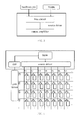
- FIG. 4 illustrates a structure of a driving circuit of an array substrate according to one embodiment of the present disclosure.
- FIG. 5 illustrates a structure of a separate driving circuit in a traditional array substrate.
- the array substrate may utilize a 1-Chip GOA (one chip gate shift register integrated on substrate) structure shown in FIG. 4 .
- 1-Chip GOA one chip gate shift register integrated on substrate
- the TCON which outputs the data voltage signal DATA, a start pulse signal LOAD, a polarity control signal POL and a clock signal CLK to the source driver, is designed as being at the same chip with the source driver, and the TCON outputs a scan start signal STV, a gate selection signal CP and an output enable signal OE to a gate driver through a Gate In panel (GIP) circuit.
- GIP Gate In panel
- the step 102 may comprise steps as follows (not shown in FIG. 1 )
- step 1021 dividing the plurality of output channels wired in a fan-out manner into at least three sectors;
- step 1022 setting the bias circuit to supply the output amplifiers corresponding to the output channels in the same sector with bias currents having the same amplitude, and bias currents corresponding to sectors far away from an axis of a fan being greater than or equal to bias currents corresponding to sectors close to the axis of the fan in amplitude.
- the step 1021 may comprises: dividing the plurality of output channels wired in the fan-out manner into at least three equal sectors whose total number is an odd number according to distances to the axis of the fan.
- FIG. 6 is an exemplary diagram illustrating a detailed manner for setting the bias currents corresponding to the respective output channels.
- a total number of the output channels of the source driver is m and these output channels are wired in the fan-out manner (a wiring length of the middle channel is short and its resistance value is small).
- the detailed manner for setting comprises a process as follows.
- the corresponding bias currents of the output amplifiers in the source driver corresponding to the first to the (f(m/15)-1)th output channels and the (m-f(m/15))th to the mth output channels of the source driver are set as maximum, namely 0 ⁇ 7.
- the corresponding bias currents of the output amplifiers in the source driver corresponding to the (f(m/15))th to the (2f(m/15)-1)th output channels and the (m-2f(m/15))th to the (m-f(m/15)-1)th output channels are set as middle maximum, namely 0 ⁇ 6.
- the corresponding bias currents of the output amplifiers in the source driver corresponding to the (2f(m/15))th to the (3f(m/15)-1)th output channels and the (m-3f(m/15))th to the (m-2f(m/15)-1)th output channels are set as large, namely 0 ⁇ 5.
- the corresponding bias currents of the output amplifiers in the source driver corresponding to the (3f(m/15))th to the (4f(m/15)-1)th output channels and the (m-4f(m/15))th to the (m-3f(m/15)-1)th output channels are set as middle large, namely 0 ⁇ 4.
- the corresponding bias currents of the output amplifiers in the source driver corresponding to the (4f(m/15))th to the (5f(m/15)-1)th output channels and the (m-5f(m/15))th to the (m-4f(m/15)-1)th output channels are set as medium, namely 0 ⁇ 3.
- the corresponding bias currents of the output amplifiers in the source driver corresponding to the (5f(m/15))th to the (6f(m/15)-1)th output channels and the (m-6f(m/15))th to the (m-5f(m/15)-1)th output channels are set as middle medium, namely 0 ⁇ 2.
- the corresponding bias currents of the output amplifiers in the source driver corresponding to the (6f(m/15))th to the (7f(m/15)-1)th output channels and the (m-7f(m/15))th to the (m-6f(m/15)-1)th output channels are set as small, namely 0 ⁇ 1.
- the corresponding bias currents of the output amplifiers in the source driver corresponding to the (7f(m/15))th to the (m-7f(m/15)-1)th output channels are set as minimum, namely 0 ⁇ 0.
- FIGS. 7-8 are exemplary diagrams illustrating two detailed manners for setting the bias currents according to embodiments of the present disclosure.
- the setting manner shown in FIG. 8 is obtained by, based on the setting manner shown in FIG.
- the present disclosure further provides a source driver comprising a plurality of output channels, a plurality of output amplifiers corresponding to the plurality of output channels and a bias circuit configured to supply the output amplifiers with bias currents.
- the source driver further comprises:
- a channel resistance acquirement module configured to acquire resistance values of the output channels
- a bias current setting module configured to, for each of the output channels, set an amplitude of the bias current supplied to the output amplifier corresponding to the output channel from the bias circuit, according to the resistance value of the respective output channel acquired by the channel resistance acquirement module, so that the bias current of the output amplifier corresponding to the output channel with a larger resistance value is greater than or equal to the bias current of the output amplifier corresponding to the output channel with a smaller resistance value in amplitude.
- the channel resistance acquirement module and/or the bias current setting module may be embodied by actual circuits or computer program.
- the channel resistance acquirement module may comprise a resistance sensor circuit configured to acquire resistance value of each output channel
- the bias current setting module may comprise a logic calculation circuit configured to calculate the TCON code corresponding to the respective output channels according to resistance values.
- the channel resistance acquirement module may be a module in a manner of computer program capable of calculating the resistance of each output channel according to circuit design parameter(s) stored in files
- the bias current setting module may be a module in a manner of computer program capable of calculating actual setting parameter(s) for the bias currents corresponding to the respective output channels according to the resistance values, and in this case, these two modules are not required to be integrated in the actual circuit of the source driver and may be existed in an external computer device or a storage medium separately.
- the bias circuit comprises a plurality of bias resistors corresponding to the plurality of output amplifiers
- the bias current setting module comprises a bias resistance setting unit configured to set the amplitudes of the bias currents supplied to the output amplifiers from the bias circuit by setting the resistance values of a plurality of bias resistors corresponding to the plurality of output amplifiers in the bias circuit.
- the bias current setting module further comprises:
- a sector division unit configured to divide the plurality of output channels wired in the fan-out manner into at least three sectors
- a sector bias current setting unit configured to set the bias circuit to supply the output amplifiers corresponding to the output channels in the same sector with bias currents having the same amplitude, and bias currents corresponding to sectors far away from an axis of a fan to be greater than or equal to bias currents corresponding to sectors close to the axis of the fan in amplitude.
- the sector division unit is further configured to divide the plurality of output channels wired in the fan-out manner into at least three equal sectors whose total number is an odd number according to distances to the axis of the fan.
- the source driver can implement any one of the driving methods for the source driver described above and has the same technical features, therefore it can settle the same technical problem and achieve the same technical effect.
- the present disclosure further provides an array substrate comprising any one of the source drivers described above.
- the array substrate has the same technical features as the any one of the source drivers described above, therefore it can settle the same technical problem and achieve the same technical effect.
- the present disclosure further provides a display apparatus comprising any one of the array substrates described above.
- the display apparatus may be: a liquid crystal display panel, a piece of electrical paper, a mobile phone, a tablet computer, a TV, a notebook computer, a digital frame, a navigator and any other products or parts having the display function.
- the display apparatus has the same technical features as the any one of the array substrates described above, therefore it can settle the same technical problem and achieve the same technical effect.
- the direction or position relationship indicated by the terms “up”, “down”, etc. are the direction or position relationship shown in drawings, which is only used to facilitate the description of the present disclosure and simplify the description, rather than indicate or suggest that a device or element must have a specific orientation, be configured or operate in the specific orientation, therefore it can not be constructed as any limitations on the present disclosure.
- the term “installation”, “connected”, “connection” should be understand broadly and generally, for example, it may be a fixed connection, a detachable connection, or a integrated connection, may be a mechanical connection or an electrical connection; may be connected directly or connected indirectly via intervening elements; or also may be an internal connection between two components.
- the specific meaning of the above terms in the present disclosure may be understood based on their specific situations.
Landscapes
- Engineering & Computer Science (AREA)
- Theoretical Computer Science (AREA)
- Physics & Mathematics (AREA)
- General Physics & Mathematics (AREA)
- Computer Hardware Design (AREA)
- General Engineering & Computer Science (AREA)
- Control Of Indicators Other Than Cathode Ray Tubes (AREA)
- Liquid Crystal Display Device Control (AREA)
- Amplifiers (AREA)
Abstract
Description
Claims (13)
Applications Claiming Priority (4)
| Application Number | Priority Date | Filing Date | Title |
|---|---|---|---|
| CN201410778976.1A CN104392688B (en) | 2014-12-15 | 2014-12-15 | Source electrode driver and its driving method, array base palte, display device |
| CN201410778976.1 | 2014-12-15 | ||
| CN201410778976 | 2014-12-15 | ||
| PCT/CN2015/081913 WO2016095467A1 (en) | 2014-12-15 | 2015-06-19 | Source driver and driving method thereof, array substrate and display device |
Publications (2)
| Publication Number | Publication Date |
|---|---|
| US20160343292A1 US20160343292A1 (en) | 2016-11-24 |
| US9934717B2 true US9934717B2 (en) | 2018-04-03 |
Family
ID=52610581
Family Applications (1)
| Application Number | Title | Priority Date | Filing Date |
|---|---|---|---|
| US14/896,810 Active 2035-08-30 US9934717B2 (en) | 2014-12-15 | 2015-06-19 | Source driver and driving method thereof, array substrate and display apparatus |
Country Status (3)
| Country | Link |
|---|---|
| US (1) | US9934717B2 (en) |
| CN (1) | CN104392688B (en) |
| WO (1) | WO2016095467A1 (en) |
Cited By (2)
| Publication number | Priority date | Publication date | Assignee | Title |
|---|---|---|---|---|
| US11257408B2 (en) | 2017-07-03 | 2022-02-22 | Boe Technology Group Co., Ltd. | Drive device and drive method for display panel, and display device |
| US12154471B2 (en) | 2019-08-09 | 2024-11-26 | Lx Semicon Co., Ltd. | Source driver controlling bias current |
Families Citing this family (9)
| Publication number | Priority date | Publication date | Assignee | Title |
|---|---|---|---|---|
| CN104392688B (en) | 2014-12-15 | 2017-08-08 | 合肥京东方光电科技有限公司 | Source electrode driver and its driving method, array base palte, display device |
| CN105118452A (en) * | 2015-08-20 | 2015-12-02 | 京东方科技集团股份有限公司 | Gate driving method and structure |
| CN105448270A (en) * | 2016-01-19 | 2016-03-30 | 京东方科技集团股份有限公司 | A display driving system and a display apparatus |
| CN107123407B (en) * | 2017-06-20 | 2019-08-02 | 深圳市华星光电技术有限公司 | A kind of drive circuit system and the liquid crystal display comprising the drive circuit system |
| CN108597466A (en) * | 2018-04-25 | 2018-09-28 | 深圳市华星光电技术有限公司 | Compensation gamma voltages improve the circuit and display device that crosstalk is coupled |
| KR102719193B1 (en) * | 2019-01-22 | 2024-10-18 | 삼성디스플레이 주식회사 | Display apparatus and method of driving display panel using the same |
| US11403991B2 (en) * | 2020-09-03 | 2022-08-02 | Tcl China Star Optoelectronics Technology Co., Ltd. | Display panel and spliced display panel |
| CN114038373A (en) * | 2021-11-18 | 2022-02-11 | Tcl华星光电技术有限公司 | Display device and driving method thereof |
| KR20250047461A (en) | 2023-09-27 | 2025-04-04 | 삼성디스플레이 주식회사 | Display apparatus and method of driving display panel using the same |
Citations (7)
| Publication number | Priority date | Publication date | Assignee | Title |
|---|---|---|---|---|
| US20030151581A1 (en) | 2002-01-25 | 2003-08-14 | Matsushita Electric Industrial Co., Ltd. | Driving voltage controller |
| US20050219181A1 (en) | 2004-03-31 | 2005-10-06 | Nec Electronics Corporation | Multi-gradation voltage generating apparatus including two gradation voltage generating circuits |
| CN101059947A (en) | 2006-04-20 | 2007-10-24 | 恩益禧电子股份有限公司 | Display and circuit for driving a display |
| CN201725544U (en) | 2010-01-21 | 2011-01-26 | 新相微电子(上海)有限公司 | Low power consumption drive circuit for liquid crystal display gate drive chip |
| US20120105393A1 (en) | 2010-10-29 | 2012-05-03 | Chengdu Boe Optoelectronics Technology Co., Ltd | Shift register unit, gate driving device and liquid crystal display |
| CN102800281A (en) | 2012-08-14 | 2012-11-28 | 昆山工研院新型平板显示技术中心有限公司 | Drive method and drive device for optimizing power dissipation of AMOLED panel |
| CN104392688A (en) | 2014-12-15 | 2015-03-04 | 合肥京东方光电科技有限公司 | Source driver and driving method thereof, array substrate and display device |
-
2014
- 2014-12-15 CN CN201410778976.1A patent/CN104392688B/en not_active Expired - Fee Related
-
2015
- 2015-06-19 US US14/896,810 patent/US9934717B2/en active Active
- 2015-06-19 WO PCT/CN2015/081913 patent/WO2016095467A1/en not_active Ceased
Patent Citations (9)
| Publication number | Priority date | Publication date | Assignee | Title |
|---|---|---|---|---|
| US20030151581A1 (en) | 2002-01-25 | 2003-08-14 | Matsushita Electric Industrial Co., Ltd. | Driving voltage controller |
| CN1453675A (en) | 2002-01-25 | 2003-11-05 | 松下电器产业株式会社 | Drive voltage controller |
| US20050219181A1 (en) | 2004-03-31 | 2005-10-06 | Nec Electronics Corporation | Multi-gradation voltage generating apparatus including two gradation voltage generating circuits |
| CN101059947A (en) | 2006-04-20 | 2007-10-24 | 恩益禧电子股份有限公司 | Display and circuit for driving a display |
| US20070247408A1 (en) | 2006-04-20 | 2007-10-25 | Nec Electronics Corporation | Display and circuit for driving a display |
| CN201725544U (en) | 2010-01-21 | 2011-01-26 | 新相微电子(上海)有限公司 | Low power consumption drive circuit for liquid crystal display gate drive chip |
| US20120105393A1 (en) | 2010-10-29 | 2012-05-03 | Chengdu Boe Optoelectronics Technology Co., Ltd | Shift register unit, gate driving device and liquid crystal display |
| CN102800281A (en) | 2012-08-14 | 2012-11-28 | 昆山工研院新型平板显示技术中心有限公司 | Drive method and drive device for optimizing power dissipation of AMOLED panel |
| CN104392688A (en) | 2014-12-15 | 2015-03-04 | 合肥京东方光电科技有限公司 | Source driver and driving method thereof, array substrate and display device |
Non-Patent Citations (3)
| Title |
|---|
| First Chinese Office Action dated Jul. 12, 2016; Appln. No. 201410778976.1. |
| International Search Report and Written Opinion both dated Sep. 24, 2015; PCT/CN2015/081913. |
| Second Chinese Office Action dated Dec. 9, 2016; Appln. No. 201410778976.1. |
Cited By (2)
| Publication number | Priority date | Publication date | Assignee | Title |
|---|---|---|---|---|
| US11257408B2 (en) | 2017-07-03 | 2022-02-22 | Boe Technology Group Co., Ltd. | Drive device and drive method for display panel, and display device |
| US12154471B2 (en) | 2019-08-09 | 2024-11-26 | Lx Semicon Co., Ltd. | Source driver controlling bias current |
Also Published As
| Publication number | Publication date |
|---|---|
| CN104392688A (en) | 2015-03-04 |
| CN104392688B (en) | 2017-08-08 |
| WO2016095467A1 (en) | 2016-06-23 |
| US20160343292A1 (en) | 2016-11-24 |
Similar Documents
| Publication | Publication Date | Title |
|---|---|---|
| US9934717B2 (en) | Source driver and driving method thereof, array substrate and display apparatus | |
| US9148134B2 (en) | Data driver, display panel driving device, and display device | |
| US8836632B2 (en) | Shift register and touch device | |
| CN104821159B (en) | Gate driving circuit, display panel and touch display device | |
| US10120482B2 (en) | Driving method for in-cell type touch display panel | |
| US10152939B2 (en) | Gate driving circuit, method for driving the same, and display device | |
| CN111489710B (en) | Display device driving method, driver, and display device | |
| US20160027371A1 (en) | Shift register unit, gate driving circuit and display device | |
| EP3217383A1 (en) | Array substrate gate drive unit, method and circuit and display device | |
| US20120280965A1 (en) | System and method for controlling the slew rate of a signal | |
| US20170316730A1 (en) | Display panels with a gate driver circuit disposed in the active area thereof | |
| US20160132170A1 (en) | Driving Unit for Touch Electrode, Driving Circuit, Touch Panel and Driving Method | |
| TWI460994B (en) | Clock feedthrough and crosstalk reduction method | |
| US20160055811A1 (en) | Gate drive circuit, array substrate and display device | |
| KR20160003102A (en) | Goa drive circuit and drive method | |
| US9319032B2 (en) | Ramp signal generating circuit and signal generator, array substrate and display apparatus | |
| US9755624B2 (en) | Ramp signal generating circuit and signal generator, array substrate and display apparatus | |
| CN109102768B (en) | Array substrate mother board and detection method thereof | |
| US12073807B2 (en) | Display apparatus and method for driving display apparatus | |
| US10446073B2 (en) | Driving method for display panel | |
| CN114822442A (en) | Scanning driving circuit, display module and display device | |
| US20170301306A1 (en) | Gate Driving Method and Device | |
| US10545606B2 (en) | Scanning circuit for touch screen, touch screen and touch control method | |
| US10832605B2 (en) | Inverter circuit and driving method thereof, array substrate and detection method thereof, and display apparatus including the same | |
| US12321546B2 (en) | Touch display device and driving method for the touch display device |
Legal Events
| Date | Code | Title | Description |
|---|---|---|---|
| AS | Assignment |
Owner name: HEFEI BOE OPTOELECTRONICS TECHNOLOGY CO., LTD., CH Free format text: ASSIGNMENT OF ASSIGNORS INTEREST;ASSIGNOR:ZHENG, LIANGLIANG;REEL/FRAME:037238/0892 Effective date: 20151207 Owner name: BOE TECHNOLOGY GROUP CO., LTD., CHINA Free format text: ASSIGNMENT OF ASSIGNORS INTEREST;ASSIGNOR:HE, JIAN;REEL/FRAME:037238/0919 Effective date: 20151207 Owner name: BOE TECHNOLOGY GROUP CO., LTD., CHINA Free format text: ASSIGNMENT OF ASSIGNORS INTEREST;ASSIGNOR:ZHENG, LIANGLIANG;REEL/FRAME:037238/0892 Effective date: 20151207 Owner name: HEFEI BOE OPTOELECTRONICS TECHNOLOGY CO., LTD., CH Free format text: ASSIGNMENT OF ASSIGNORS INTEREST;ASSIGNOR:HE, JIAN;REEL/FRAME:037238/0919 Effective date: 20151207 |
|
| STCF | Information on status: patent grant |
Free format text: PATENTED CASE |
|
| MAFP | Maintenance fee payment |
Free format text: PAYMENT OF MAINTENANCE FEE, 4TH YEAR, LARGE ENTITY (ORIGINAL EVENT CODE: M1551); ENTITY STATUS OF PATENT OWNER: LARGE ENTITY Year of fee payment: 4 |
|
| FEPP | Fee payment procedure |
Free format text: MAINTENANCE FEE REMINDER MAILED (ORIGINAL EVENT CODE: REM.); ENTITY STATUS OF PATENT OWNER: LARGE ENTITY |