US9934336B2 - Method of correcting electron proximity effects using Voigt type scattering functions - Google Patents
Method of correcting electron proximity effects using Voigt type scattering functions Download PDFInfo
- Publication number
- US9934336B2 US9934336B2 US13/861,284 US201313861284A US9934336B2 US 9934336 B2 US9934336 B2 US 9934336B2 US 201313861284 A US201313861284 A US 201313861284A US 9934336 B2 US9934336 B2 US 9934336B2
- Authority
- US
- United States
- Prior art keywords
- function
- electron beam
- wafer
- point spread
- mask
- Prior art date
- Legal status (The legal status is an assumption and is not a legal conclusion. Google has not performed a legal analysis and makes no representation as to the accuracy of the status listed.)
- Active
Links
Images


Classifications
-
- G—PHYSICS
- G03—PHOTOGRAPHY; CINEMATOGRAPHY; ANALOGOUS TECHNIQUES USING WAVES OTHER THAN OPTICAL WAVES; ELECTROGRAPHY; HOLOGRAPHY
- G03F—PHOTOMECHANICAL PRODUCTION OF TEXTURED OR PATTERNED SURFACES, e.g. FOR PRINTING, FOR PROCESSING OF SEMICONDUCTOR DEVICES; MATERIALS THEREFOR; ORIGINALS THEREFOR; APPARATUS SPECIALLY ADAPTED THEREFOR
- G03F1/00—Originals for photomechanical production of textured or patterned surfaces, e.g., masks, photo-masks, reticles; Mask blanks or pellicles therefor; Containers specially adapted therefor; Preparation thereof
- G03F1/36—Masks having proximity correction features; Preparation thereof, e.g. optical proximity correction [OPC] design processes
-
- G06F17/5009—
-
- G—PHYSICS
- G06—COMPUTING OR CALCULATING; COUNTING
- G06F—ELECTRIC DIGITAL DATA PROCESSING
- G06F30/00—Computer-aided design [CAD]
- G06F30/30—Circuit design
- G06F30/32—Circuit design at the digital level
- G06F30/33—Design verification, e.g. functional simulation or model checking
- G06F30/3308—Design verification, e.g. functional simulation or model checking using simulation
-
- B—PERFORMING OPERATIONS; TRANSPORTING
- B82—NANOTECHNOLOGY
- B82Y—SPECIFIC USES OR APPLICATIONS OF NANOSTRUCTURES; MEASUREMENT OR ANALYSIS OF NANOSTRUCTURES; MANUFACTURE OR TREATMENT OF NANOSTRUCTURES
- B82Y10/00—Nanotechnology for information processing, storage or transmission, e.g. quantum computing or single electron logic
-
- B—PERFORMING OPERATIONS; TRANSPORTING
- B82—NANOTECHNOLOGY
- B82Y—SPECIFIC USES OR APPLICATIONS OF NANOSTRUCTURES; MEASUREMENT OR ANALYSIS OF NANOSTRUCTURES; MANUFACTURE OR TREATMENT OF NANOSTRUCTURES
- B82Y40/00—Manufacture or treatment of nanostructures
-
- G—PHYSICS
- G03—PHOTOGRAPHY; CINEMATOGRAPHY; ANALOGOUS TECHNIQUES USING WAVES OTHER THAN OPTICAL WAVES; ELECTROGRAPHY; HOLOGRAPHY
- G03F—PHOTOMECHANICAL PRODUCTION OF TEXTURED OR PATTERNED SURFACES, e.g. FOR PRINTING, FOR PROCESSING OF SEMICONDUCTOR DEVICES; MATERIALS THEREFOR; ORIGINALS THEREFOR; APPARATUS SPECIALLY ADAPTED THEREFOR
- G03F7/00—Photomechanical, e.g. photolithographic, production of textured or patterned surfaces, e.g. printing surfaces; Materials therefor, e.g. comprising photoresists; Apparatus specially adapted therefor
- G03F7/20—Exposure; Apparatus therefor
- G03F7/2037—Exposure with X-ray radiation or corpuscular radiation, through a mask with a pattern opaque to that radiation
-
- G—PHYSICS
- G03—PHOTOGRAPHY; CINEMATOGRAPHY; ANALOGOUS TECHNIQUES USING WAVES OTHER THAN OPTICAL WAVES; ELECTROGRAPHY; HOLOGRAPHY
- G03F—PHOTOMECHANICAL PRODUCTION OF TEXTURED OR PATTERNED SURFACES, e.g. FOR PRINTING, FOR PROCESSING OF SEMICONDUCTOR DEVICES; MATERIALS THEREFOR; ORIGINALS THEREFOR; APPARATUS SPECIALLY ADAPTED THEREFOR
- G03F7/00—Photomechanical, e.g. photolithographic, production of textured or patterned surfaces, e.g. printing surfaces; Materials therefor, e.g. comprising photoresists; Apparatus specially adapted therefor
- G03F7/20—Exposure; Apparatus therefor
- G03F7/2051—Exposure without an original mask, e.g. using a programmed deflection of a point source, by scanning, by drawing with a light beam, using an addressed light or corpuscular source
- G03F7/2059—Exposure without an original mask, e.g. using a programmed deflection of a point source, by scanning, by drawing with a light beam, using an addressed light or corpuscular source using a scanning corpuscular radiation beam, e.g. an electron beam
- G03F7/2061—Electron scattering (proximity) correction or prevention methods
-
- G—PHYSICS
- G06—COMPUTING OR CALCULATING; COUNTING
- G06F—ELECTRIC DIGITAL DATA PROCESSING
- G06F30/00—Computer-aided design [CAD]
- G06F30/20—Design optimisation, verification or simulation
-
- H—ELECTRICITY
- H01—ELECTRIC ELEMENTS
- H01J—ELECTRIC DISCHARGE TUBES OR DISCHARGE LAMPS
- H01J37/00—Discharge tubes with provision for introducing objects or material to be exposed to the discharge, e.g. for the purpose of examination or processing thereof
- H01J37/02—Details
- H01J37/22—Optical, image processing or photographic arrangements associated with the tube
- H01J37/222—Image processing arrangements associated with the tube
-
- H—ELECTRICITY
- H01—ELECTRIC ELEMENTS
- H01J—ELECTRIC DISCHARGE TUBES OR DISCHARGE LAMPS
- H01J37/00—Discharge tubes with provision for introducing objects or material to be exposed to the discharge, e.g. for the purpose of examination or processing thereof
- H01J37/30—Electron-beam or ion-beam tubes for localised treatment of objects
- H01J37/317—Electron-beam or ion-beam tubes for localised treatment of objects for changing properties of the objects or for applying thin layers thereon, e.g. for ion implantation
- H01J37/3174—Particle-beam lithography, e.g. electron beam lithography
-
- H—ELECTRICITY
- H10—SEMICONDUCTOR DEVICES; ELECTRIC SOLID-STATE DEVICES NOT OTHERWISE PROVIDED FOR
- H10P—GENERIC PROCESSES OR APPARATUS FOR THE MANUFACTURE OR TREATMENT OF DEVICES COVERED BY CLASS H10
- H10P76/00—Manufacture or treatment of masks on semiconductor bodies, e.g. by lithography or photolithography
- H10P76/20—Manufacture or treatment of masks on semiconductor bodies, e.g. by lithography or photolithography of masks comprising organic materials
- H10P76/204—Manufacture or treatment of masks on semiconductor bodies, e.g. by lithography or photolithography of masks comprising organic materials of organic photoresist masks
- H10P76/2041—Photolithographic processes
-
- H—ELECTRICITY
- H01—ELECTRIC ELEMENTS
- H01J—ELECTRIC DISCHARGE TUBES OR DISCHARGE LAMPS
- H01J2237/00—Discharge tubes exposing object to beam, e.g. for analysis treatment, etching, imaging
- H01J2237/22—Treatment of data
- H01J2237/226—Image reconstruction
-
- H—ELECTRICITY
- H01—ELECTRIC ELEMENTS
- H01J—ELECTRIC DISCHARGE TUBES OR DISCHARGE LAMPS
- H01J2237/00—Discharge tubes exposing object to beam, e.g. for analysis treatment, etching, imaging
- H01J2237/30—Electron or ion beam tubes for processing objects
- H01J2237/317—Processing objects on a microscale
- H01J2237/3175—Lithography
- H01J2237/31769—Proximity effect correction
Definitions
- the present invention applies notably to the field of electron lithography for direct on-wafer etching or for fabricating masks. More generally, it applies to any field where it is required to model the interaction of a beam of electrons with a target, this also being the case in electron microscopy, notably for the inspection of wafers and masks.
- This interaction is notably affected by a scattering of the electrons around the initial trajectory (forward scattering effect) as well as by a backscattering (backward scattering effect).
- These effects referred to as proximity effects, depend notably on the materials of the target and its geometry. Whatever the reason for desiring to perform this electron bombardment (etching, imaging or analysis), it is therefore necessary to take account of the proximity effects in order to obtain a result which is faithful to the objective sought. A correction of the proximity effects is therefore performed. Accordingly, it is known to predict them through a model so as to take account thereof in the calculation of the electron radiation doses used to bombard the target.
- PSF point spread or scattering function
- the present invention solves the problem posed by the deviations of modeling of the proximity effects by using a class of PSF combining Lorentzian functions with Gaussian functions, for example a Voigt function, or approximations of these functions.
- the invention envisages a method for projecting an electron beam onto a wafer or a mask comprising a step of correcting the effects of scattering of said beam, said step comprising a sub-step of calculating a point spread function, wherein said point spread function is a linear combination of functions chosen from a group comprising at least one Voigt function ( 230 ) and a function approximating a Voigt function.
- said at least one function approximating a Voigt function is a Pearson VII function.
- said linear combination of functions also comprises at least one Gaussian function.
- the sub-step of calculating a point spread function comprises a sub-step of selection of the parameters of said functions which are included in the linear combination and of the coefficients of said linear combination, said selection sub-step comprising an execution of an optimization function of the fit of the point spread function with a set of experimental results or with a representation of a Monte-Carlo simulation of the scattering of the radiation on the target.
- said at least one function has an extremum which is not located at the center of the beam.
- said at least one function has an extremum which is located on a backward scattering peak of the electron beam.
- said point spread function is a linear combination of at least as many functions as the radiation comprises backward scattering peaks.
- the invention also envisages a computer program comprising program code instructions configured for the execution of a method for projecting an electron beam on a wafer or a mask of claim 1 when the program is executed on a computer, said program comprising a module for simulating and/or correcting the scattering effects in said beam, said module comprising a sub-module for calculating a point spread function, wherein said point spread function is a linear combination of functions chosen from a group comprising at least one Voigt function and a function approximating a Voigt function.
- the invention also covers an electron lithography system comprising a module for projecting an electron beam onto a wafer or a mask and a computer program having the characteristics defined hereinabove.
- the invention also covers a system for simulating at least one electron lithography step comprising a module for simulating a step of projecting an electron beam onto a wafer or a mask and a computer program having the characteristics defined hereinabove.
- the invention also covers an electron microscopy system comprising a module for projecting an electron beam onto a wafer or a mask and a computer program having the characteristics defined hereinabove.
- the classes of function used in this embodiment have an analytical expression and they can easily be integrated into off-the-shelf tools without significant modification.
- the cumulative distribution function being analytical itself, the convolution calculations which are necessary for the correction of the proximity effects remain of the same order of computational complexity as the solutions of the prior art.
- FIG. 1 represents the distribution of energy absorbed by a resin according to a reference model
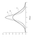
- FIG. 2 represents a Gaussian function, a Lorentz function and a Voigt function
- FIGS. 3 a and 3 b represent the distribution of energy absorbed by a resin or by a mask insulated under extreme UV according to one embodiment of the invention
- FIGS. 4 a to 4 f represent the distribution of energy absorbed in various scenarios of use of the invention.
- FIG. 1 represents the distribution of energy absorbed by a resin according to a reference model.
- the publication CASINO V2.42 (“A Fast and Easy-to-use Modeling Tool for Scanning Electron Microscopy and Microanalysis Users”, Scanning, vol. 29, 92-101 (2007), D. Drouin et al) sets forth the operation of software for simulating the energy distribution of an electron beam by the Monte-Carlo procedure.
- the software makes it possible to best describe how the energy is distributed around the center of the beam of electrons by choosing the parameters of various possible physical models of interaction between the electrons and the target of the beam, nature of the materials and thicknesses of the layers mainly.
- the object of the invention is to replace at least one of the Gaussian functions of the PSF by another function so as to obtain a better fit with the distribution curves of of the type of those represented on FIG. 1 which correspond to the reference model.
- FIG. 2 represents a Gaussian function, a Lorentz function and a Voigt function.
- Voigt type functions which are the convolution product of a Gaussian function and of a Lorentzian function or sufficiently accurate approximations of these functions, improve the fit with the reference model.
- a Voigt function of a distance ⁇ to the center of the beam ⁇ c is calculated via the convolution formula:
- y ⁇ ( x ) ⁇ - ⁇ + ⁇ ⁇ ( e ( ( x - t ) - x c a ) 2 ( 1 1 + ( t - x c b ) 2 ) ) ⁇ ⁇ d ⁇ ⁇ t in which a is the standard deviation of the Gauss function and b is the half-width at mid-height of the Lorenz function, the height being the value of said function at
- the three functions are represented in the figure: a Gaussian function, by the curve 210 , a Lorentzian function by the curve 220 and a Voigt function by the curve 230 .
- FIGS. 3 a and 3 b represent the distribution of energy absorbed by a resin or by a mask insulated under extreme UV according to one embodiment of the invention.
- FIG. 3 a is represented, purely by way of non-limiting illustration of the generality of the invention, an embodiment of the invention in which a mask adapted for this use (that is to say consisting for example of a glass support covered with a chromium or tantalum absorber) is subjected to a radiation.
- the reference model given by curve 310 a is determined by the CASINO simulation software using the ESELPA database which accurately gives the collision cross sections for electrons colliding with matter in a wide energy range.
- Four Pearson VII functions are combined to produce the PSF 360 a:
- FIG. 3 b is represented, purely by way of non-limiting illustration of the generality of the invention, an embodiment of the invention in which a substrate covered with a resin, for example PMMA, receives a radiation.
- the representations and notation are the same as those of FIG. 3 a .
- the Pearson VII functions which are used are identical to those of FIG. 3 a .
- the only change is the coefficients Ai of the linear combination. They have in this case the following values:
- FIGS. 4 a to 4 f represent the distribution of energy absorbed in various scenarios of use of the invention.
- the radiation curve for the reference model 410 a is compared with the PSF calculated according to the method of the invention 420 a for the sum of four Voigt functions and with those calculated according to the conventional methodology 430 a consisting in using a sum of four Gaussian functions.
- the radiation is emitted by a small beam (of 2 nm in the illustrative example of these figures).
- FIG. 4 a is illustrated a case in which the target is a 100-nm PMMA stack on silicon substrate, the radiation having an energy of 100 keV.
- FIG. 4 b is illustrated a case in which the target is an EUV (extreme UV) stack, the radiation having an energy of 100 keV.
- EUV extreme UV
- FIG. 4 c is illustrated a case in which the target is a 100-nm PMMA stack on silicon substrate, the radiation having an energy of 50 keV.
- FIG. 4 d is illustrated a case in which the target is an EUV (extreme UV) stack, the radiation having an energy of 50 keV.
- EUV extreme UV
- FIG. 4 e is illustrated a case in which the target is a 100-nm PMMA stack on silicon substrate, the radiation having an energy of 10 keV.
- FIG. 4 f is illustrated a case in which the target is a 100-nm PMMA stack on silicon substrate, the radiation consisting of a broad beam (30 nm) having an energy of 100 keV.
- the method of the invention can, however, also be implemented in other usage conditions.
- the Voigt functions or the Pearson VII functions are chosen in such a way that the resulting distribution is centered or non-centered with respect to the center of the electron beam.
- An off-centering of certain peaks is conceivable for conditions where the backscatter becomes predominant.
- the center of the distribution is adjusted to the backward scattering peak (backscatter).
- backscatter backward scattering peak
- Dose modulation may for example be performed, according to the invention, by modifying dose modulation software, for example the PROXECCOTM software distributed by the company SynopsisTM or the InscalTM software from the company Aselta NanographicsTM to replace the PSF of the backscattering of the prior art by the PSF of the backscattering described hereinabove.
- dose modulation software for example the PROXECCOTM software distributed by the company SynopsisTM or the InscalTM software from the company Aselta NanographicsTM to replace the PSF of the backscattering of the prior art by the PSF of the backscattering described hereinabove.
- For the forward scattering PSF it will be possible to use as in the prior art a centered Gaussian or any other type of bell curve centered on the center of the beam.
- Dose modulation is performed by convolving the PSF (PSF of the forward scattering and PSF of the backscattering) with the geometry of the pattern to be etched.
- the software can also be advantageously modified to carry out combined optimization of the dose modulation and of the geometry of the pattern to be etched, according to a method such as that described in international application PCT/EP2011/05583 licensed to one of the applicants of the present patent application.
- the method of the invention and the computer program for implementing it can also be used to optimize the PSF of scanning, field-effect or tunnel-effect electron microscopy systems which can be used in imaging or to carry out the inspection of wafers or masks. They can also be adapted for carrying out a simulation of one or more steps of an electron lithography method.
Landscapes
- Engineering & Computer Science (AREA)
- Physics & Mathematics (AREA)
- Chemical & Material Sciences (AREA)
- General Physics & Mathematics (AREA)
- Theoretical Computer Science (AREA)
- Nanotechnology (AREA)
- Analytical Chemistry (AREA)
- Computer Hardware Design (AREA)
- Toxicology (AREA)
- Health & Medical Sciences (AREA)
- Crystallography & Structural Chemistry (AREA)
- Computer Vision & Pattern Recognition (AREA)
- Evolutionary Computation (AREA)
- Geometry (AREA)
- General Engineering & Computer Science (AREA)
- Manufacturing & Machinery (AREA)
- Condensed Matter Physics & Semiconductors (AREA)
- Mathematical Physics (AREA)
- Electron Beam Exposure (AREA)
Abstract
Description
With the following notation:
-
- α is the width of the direct radiation;
- β is the backscattering width;
- η is the ratio of the intensities of the direct and backscattered radiations.
- ξ is the radial position of a point
The values of the parameters α, β and η can be determined experimentally for a given method. These parameters are dependent on the acceleration voltage of the machine and the target. Typically for an acceleration voltage of the order of 50 KV and a silicon or glass target (SiO2), α is of the order of 30 nm, β of the order of 10 μm and η of the order of 0.5.
in which a is the standard deviation of the Gauss function and b is the half-width at mid-height of the Lorenz function, the height being the value of said function at
in which M is the shape parameter or Pearson width and w a distance giving the width at mid-height FWHM (Full Width at Half Maximum) of the Pearson peak. When M<<1, the shape of the curve approximates a Lorentz curve. When M>>10, the shape of the curve approximates a Gauss curve.
-
- A first Pearson1 function, represented by
curve 320 a, is a Pearson VII function whose parameters M and w are fixed respectively at 3 and 2.2 nm; - A second Pearson2 function, represented by
curve 330 a, is a Pearson VII function whose parameters M and w are fixed respectively at 1.7 and 8 nm; - A third Pearson3 function, represented by
curve 340 a, is a Pearson VII function whose parameters M and w are fixed respectively at 1.5 and 1200 nm; - A fourth Pearson4 function, represented by
curve 350 a, is a Pearson VII function whose parameters M and w are fixed respectively at 50 and 300 microns.
The PSF is the linear combination of the four Pearson VII functions of formula:
PSF=Pearson1×A1+Pearson2×A2+Pearson3×A3 +Pearson4×A4
In which the coefficients of the combination have the following values: - A1 such that log(A1)=−1.25;
- A2 such that log(A2)=−3.7;
- A3 such that log(A3)=−8.5;
- A4 such that log(A4)=−10.
- A first Pearson1 function, represented by
-
- A1 such that log(A1)=−1.25;
- A2 such that log(A2)=−5.4;
- A3 such that log(A3)=−10;
- A4 such that log(A4)=−11.2.
These values make it possible to obtain a better fit with the reference model.
Claims (14)
Applications Claiming Priority (2)
| Application Number | Priority Date | Filing Date | Title |
|---|---|---|---|
| FR1253389A FR2989513B1 (en) | 2012-04-12 | 2012-04-12 | METHOD FOR CORRECTING ELECTRONIC PROXIMITY EFFECTS USING VOIGT-TYPE DIFFUSION FUNCTIONS |
| FR1253389 | 2012-04-12 |
Publications (2)
| Publication Number | Publication Date |
|---|---|
| US20130275098A1 US20130275098A1 (en) | 2013-10-17 |
| US9934336B2 true US9934336B2 (en) | 2018-04-03 |
Family
ID=48045369
Family Applications (1)
| Application Number | Title | Priority Date | Filing Date |
|---|---|---|---|
| US13/861,284 Active US9934336B2 (en) | 2012-04-12 | 2013-04-11 | Method of correcting electron proximity effects using Voigt type scattering functions |
Country Status (6)
| Country | Link |
|---|---|
| US (1) | US9934336B2 (en) |
| EP (1) | EP2650902B1 (en) |
| JP (1) | JP6239253B2 (en) |
| KR (1) | KR102115314B1 (en) |
| FR (1) | FR2989513B1 (en) |
| TW (1) | TWI590287B (en) |
Families Citing this family (5)
| Publication number | Priority date | Publication date | Assignee | Title |
|---|---|---|---|---|
| JPH0647952B2 (en) | 1990-03-12 | 1994-06-22 | 三井造船株式会社 | Cogeneration system |
| EP2983193B1 (en) | 2014-08-05 | 2021-10-20 | Aselta Nanographics | Method for determining the parameters of an ic manufacturing process model |
| WO2016106347A1 (en) * | 2014-12-22 | 2016-06-30 | The Research Foundation For The State University Of New York | Determination of spatial distribution of charged particle beams |
| EP3121833A1 (en) | 2015-07-20 | 2017-01-25 | Aselta Nanographics | A method of performing dose modulation, in particular for electron beam lithography |
| FR3052910B1 (en) | 2016-06-16 | 2018-06-22 | Commissariat A L'energie Atomique Et Aux Energies Alternatives | METHOD FOR PROJECTING A BEAM OF PARTICLES ON A SUBSTRATE WITH CORRECTION OF BROADCAST EFFECTS |
Citations (13)
| Publication number | Priority date | Publication date | Assignee | Title |
|---|---|---|---|---|
| JP2001083109A (en) | 1999-09-09 | 2001-03-30 | Rigaku Corp | Method and apparatus for x-ray fluorescent analysis |
| JP2002075818A (en) | 2000-08-24 | 2002-03-15 | Toshiba Corp | Method for calculating charged energy exposure energy distribution, simulator, charged beam exposure method, method of manufacturing semiconductor device and mask, recording medium storing program for calculating charged energy exposure energy distribution |
| JP2006222230A (en) | 2005-02-09 | 2006-08-24 | Semiconductor Leading Edge Technologies Inc | Proximity effect correction method |
| US20070021938A1 (en) * | 2005-07-21 | 2007-01-25 | Fujitsu Limited | Parameter extracting method |
| US20080067446A1 (en) * | 2006-06-22 | 2008-03-20 | Pdf Solutions, Inc. | Method for electron beam proximity effect correction |
| US20090162789A1 (en) * | 2006-05-05 | 2009-06-25 | Commissariat A L'energie Atomique | Method for Transferring a Predetermined Pattern Reducing Proximity Effects |
| US20110226970A1 (en) * | 2010-03-22 | 2011-09-22 | Taiwan Semiconductor Manufacturing Company, Ltd. | System and method for generating direct-write pattern |
| WO2012084091A1 (en) | 2010-12-24 | 2012-06-28 | Volkswagen Aktiengesellschaft | Exhaust system with hc adsorber and parallel exhaust-gas catalytic converter, and vehicle having an exhaust system of said type |
| TW201248755A (en) | 2011-04-28 | 2012-12-01 | Nanda Technologies Gmbh | Methods of inspecting and manufacturing semiconductor wafers |
| US20120314198A1 (en) * | 2011-06-10 | 2012-12-13 | Sang-Hee Lee | Methods of estimating point spread functions in electron-beam lithography processes |
| US20130043389A1 (en) | 2011-08-16 | 2013-02-21 | Aselta Nanographics | Method for correcting electronic proximity effects using off-center scattering functions |
| US20130201468A1 (en) * | 2010-04-15 | 2013-08-08 | Commissariat A L'energie Atomique Et Aux Energies Alternatives | Lithography method with combined optimization of radiated energy and design geometry |
| US20130239071A1 (en) * | 2012-03-07 | 2013-09-12 | Taiwan Semiconductor Manufacturing Company, Ltd. | Method and apparatus for enhanced optical proximity correction |
Family Cites Families (1)
| Publication number | Priority date | Publication date | Assignee | Title |
|---|---|---|---|---|
| EP1997620B1 (en) * | 2006-03-17 | 2016-06-15 | National Institute of Advanced Industrial Science and Technology | Laminated body and carbon film deposition method |
-
2012
- 2012-04-12 FR FR1253389A patent/FR2989513B1/en not_active Expired - Fee Related
-
2013
- 2013-03-26 TW TW102110701A patent/TWI590287B/en active
- 2013-04-11 EP EP13163244.0A patent/EP2650902B1/en active Active
- 2013-04-11 JP JP2013082602A patent/JP6239253B2/en active Active
- 2013-04-11 US US13/861,284 patent/US9934336B2/en active Active
- 2013-04-12 KR KR1020130040284A patent/KR102115314B1/en active Active
Patent Citations (14)
| Publication number | Priority date | Publication date | Assignee | Title |
|---|---|---|---|---|
| JP2001083109A (en) | 1999-09-09 | 2001-03-30 | Rigaku Corp | Method and apparatus for x-ray fluorescent analysis |
| JP2002075818A (en) | 2000-08-24 | 2002-03-15 | Toshiba Corp | Method for calculating charged energy exposure energy distribution, simulator, charged beam exposure method, method of manufacturing semiconductor device and mask, recording medium storing program for calculating charged energy exposure energy distribution |
| JP2006222230A (en) | 2005-02-09 | 2006-08-24 | Semiconductor Leading Edge Technologies Inc | Proximity effect correction method |
| US20070021938A1 (en) * | 2005-07-21 | 2007-01-25 | Fujitsu Limited | Parameter extracting method |
| US20090162789A1 (en) * | 2006-05-05 | 2009-06-25 | Commissariat A L'energie Atomique | Method for Transferring a Predetermined Pattern Reducing Proximity Effects |
| US20080067446A1 (en) * | 2006-06-22 | 2008-03-20 | Pdf Solutions, Inc. | Method for electron beam proximity effect correction |
| US20110226970A1 (en) * | 2010-03-22 | 2011-09-22 | Taiwan Semiconductor Manufacturing Company, Ltd. | System and method for generating direct-write pattern |
| US20130201468A1 (en) * | 2010-04-15 | 2013-08-08 | Commissariat A L'energie Atomique Et Aux Energies Alternatives | Lithography method with combined optimization of radiated energy and design geometry |
| WO2012084091A1 (en) | 2010-12-24 | 2012-06-28 | Volkswagen Aktiengesellschaft | Exhaust system with hc adsorber and parallel exhaust-gas catalytic converter, and vehicle having an exhaust system of said type |
| TW201248755A (en) | 2011-04-28 | 2012-12-01 | Nanda Technologies Gmbh | Methods of inspecting and manufacturing semiconductor wafers |
| US20120314198A1 (en) * | 2011-06-10 | 2012-12-13 | Sang-Hee Lee | Methods of estimating point spread functions in electron-beam lithography processes |
| US20130043389A1 (en) | 2011-08-16 | 2013-02-21 | Aselta Nanographics | Method for correcting electronic proximity effects using off-center scattering functions |
| FR2979165A1 (en) | 2011-08-16 | 2013-02-22 | Commissariat Energie Atomique | METHOD FOR CORRECTING ELECTRONIC PROXIMITY EFFECTS USING DECENTRED DIFFUSION FUNCTIONS |
| US20130239071A1 (en) * | 2012-03-07 | 2013-09-12 | Taiwan Semiconductor Manufacturing Company, Ltd. | Method and apparatus for enhanced optical proximity correction |
Non-Patent Citations (10)
| Title |
|---|
| "Peak Fitting Module," 2002, OriginLab Corporation, 124 pages. * |
| "Peak Shape Functions," Jan. 25, 2009, Wayback Machine archive of http://pd.chem.ucl.ac.uk/pdnn/peaks/others.htm, two pages. * |
| A.S. Kirov, et al., "Towards Two-Dimensional Brachytherapy Dosimetry Using Plastic Scintillator: Localization of the Scintillation Process", Nuclear Instruments and Methods in Physics Research Section A: Accelerators, Spectrometers, Detectors, and Associated Equipment, Jan. 1, 2000, pp. 178-188, vol. 439, No. 1, Elsevier Science B.V., Netherlands, XP004253721. |
| D.C.W. Sanderson, "Thick Source Beta Counting (TSBC): A Rapid Method for Measuring Beta Dose-Rates," Nucl. Tracks Radiat. Meas., vol. 14, Nos. 1/2, 1988, pp. 203-207. |
| Dominique Drouin, et al., "Casino V2.42—A Fast and Easy-to-use Modeling Tool for Scanning Electron Microscopy and Microanalysis Users", Scanning vol. 29, 92-101 (2007). Wiley Periodicals, Inc. |
| Fumihiro Koba et al., "Highly accurate proximity effect correction for 100kV electron projection lithography," 2005, Japanese Journal of Applied Physics, vol. 44, No. 7B, pp. 5590-5594. * |
| KIROV, A.S. BINNS, W.R. DEMPSEY, J.F. EPSTEIN, J.W. DOWKONTT, P.F. SHRINIVAS, S. HURLBUT, C. WILLIAMSON, J.F.: "Towards two-dimensional brachytherapy dosimetry using plastic scintillator: localization of the scintillation process", NUCLEAR INSTRUMENTS & METHODS IN PHYSICS RESEARCH. SECTION A: ACCELERATORS, SPECTROMETERS, DETECTORS, AND ASSOCIATED EQUIPMENT, ELSEVIER BV * NORTH-HOLLAND, NL, vol. 439, no. 1, 1 January 2000 (2000-01-01), NL, pages 178 - 188, XP004253721, ISSN: 0168-9002, DOI: 10.1016/S0168-9002(99)00894-3 |
| Office Action in Japanese Patent Application No. 2013-082602, dated Dec. 6, 2016. |
| Paul J.M. van Adrichem et al., "Data Preparation," 2005, in "Handbook of Photomask Manufacturing Technology," Taylor & Francis, 25 pages. * |
| Search Report in Taiwanese Patent Application No. 102110701, dated Oct. 5, 2016. |
Also Published As
| Publication number | Publication date |
|---|---|
| JP6239253B2 (en) | 2017-11-29 |
| EP2650902B1 (en) | 2019-11-13 |
| FR2989513B1 (en) | 2015-04-17 |
| KR20130116201A (en) | 2013-10-23 |
| JP2013222968A (en) | 2013-10-28 |
| TW201405622A (en) | 2014-02-01 |
| TWI590287B (en) | 2017-07-01 |
| FR2989513A1 (en) | 2013-10-18 |
| EP2650902A3 (en) | 2017-06-14 |
| EP2650902A2 (en) | 2013-10-16 |
| KR102115314B1 (en) | 2020-05-26 |
| US20130275098A1 (en) | 2013-10-17 |
Similar Documents
| Publication | Publication Date | Title |
|---|---|---|
| KR102154105B1 (en) | Method and system for forming patterns using charged particle beam lithograph | |
| JP5480555B2 (en) | Charged particle beam drawing apparatus and charged particle beam drawing method | |
| US7939246B2 (en) | Charged particle beam projection method | |
| US10522328B2 (en) | Method of performing dose modulation, in particular for electron beam lithography | |
| EP2978010B1 (en) | Program for correcting charged particle radiation location, device for calculating degree of correction of charged particle radiation location, charged particle radiation system, and method for correcting charged particle radiation location | |
| US9934336B2 (en) | Method of correcting electron proximity effects using Voigt type scattering functions | |
| US6835942B2 (en) | Method for correcting a proximity effect, an exposure method, a manufacturing method of a semiconductor device and a proximity correction module | |
| US20120104286A1 (en) | Method for resizing pattern to be written by lithography technique, and charged particle beam writing method | |
| US9224577B2 (en) | Method for correcting electronic proximity effects using off-center scattering functions | |
| US20190004429A1 (en) | Method for acquiring parameter for dose correction of charged particle beam, charged particle beam writing method, and charged particle beam writing apparatus | |
| KR20110063806A (en) | Method for designing and manufacturing reticles using variable shaping beam lithography | |
| JP5731257B2 (en) | Charged particle beam drawing apparatus and charged particle beam drawing method | |
| US10156796B2 (en) | Method for determining the parameters of an IC manufacturing process by a differential procedure | |
| JP5437124B2 (en) | Charged particle beam drawing method and charged particle beam drawing apparatus | |
| JP2010219285A (en) | Charged particle beam drawing method and apparatus | |
| Dersch et al. | Impact of EUV mask pattern profile shape on CD measured by CD-SEM | |
| Choi et al. | Pattern placement error due to resist charging effect at 50kV e-beam writer: mechanism and its correction | |
| Raghunathan | The effect of energy deposition on pattern resolution in electron beam lithography | |
| Mas et al. | A novel model building flow for the simulation of proximity effects of mask processes | |
| JP2006165280A (en) | Mask transfer shape prediction method and mask correction method | |
| JP2008107847A (en) | Process management method, semiconductor device manufacturing method, photomask manufacturing method, and program |
Legal Events
| Date | Code | Title | Description |
|---|---|---|---|
| AS | Assignment |
Owner name: ASELTA NANOGRAPHICS, FRANCE Free format text: ASSIGNMENT OF ASSIGNORS INTEREST;ASSIGNORS:TORTAI, JEAN-HERVE;SCHIAVONE, PATRICK;FIGUEIRO, THIAGO;AND OTHERS;SIGNING DATES FROM 20130507 TO 20130517;REEL/FRAME:030552/0268 |
|
| STCF | Information on status: patent grant |
Free format text: PATENTED CASE |
|
| MAFP | Maintenance fee payment |
Free format text: PAYMENT OF MAINTENANCE FEE, 4TH YR, SMALL ENTITY (ORIGINAL EVENT CODE: M2551); ENTITY STATUS OF PATENT OWNER: SMALL ENTITY Year of fee payment: 4 |
|
| AS | Assignment |
Owner name: APPLIED MATERIALS, INC., CALIFORNIA Free format text: ASSIGNMENT OF ASSIGNORS INTEREST;ASSIGNOR:ASELTA NANOGRAPHICS;REEL/FRAME:065739/0682 Effective date: 20221222 |
|
| MAFP | Maintenance fee payment |
Free format text: PAYMENT OF MAINTENANCE FEE, 8TH YR, SMALL ENTITY (ORIGINAL EVENT CODE: M2552); ENTITY STATUS OF PATENT OWNER: SMALL ENTITY Year of fee payment: 8 |