US9917357B2 - Antenna system - Google Patents
Antenna system Download PDFInfo
- Publication number
- US9917357B2 US9917357B2 US13/911,765 US201313911765A US9917357B2 US 9917357 B2 US9917357 B2 US 9917357B2 US 201313911765 A US201313911765 A US 201313911765A US 9917357 B2 US9917357 B2 US 9917357B2
- Authority
- US
- United States
- Prior art keywords
- antenna
- feed
- radiating element
- circuit board
- radiating
- Prior art date
- Legal status (The legal status is an assumption and is not a legal conclusion. Google has not performed a legal analysis and makes no representation as to the accuracy of the status listed.)
- Expired - Fee Related, expires
Links
Images


Classifications
-
- H—ELECTRICITY
- H01—ELECTRIC ELEMENTS
- H01Q—ANTENNAS, i.e. RADIO AERIALS
- H01Q1/00—Details of, or arrangements associated with, antennas
- H01Q1/36—Structural form of radiating elements, e.g. cone, spiral, umbrella; Particular materials used therewith
- H01Q1/38—Structural form of radiating elements, e.g. cone, spiral, umbrella; Particular materials used therewith formed by a conductive layer on an insulating support
-
- H—ELECTRICITY
- H01—ELECTRIC ELEMENTS
- H01Q—ANTENNAS, i.e. RADIO AERIALS
- H01Q1/00—Details of, or arrangements associated with, antennas
- H01Q1/12—Supports; Mounting means
- H01Q1/22—Supports; Mounting means by structural association with other equipment or articles
- H01Q1/24—Supports; Mounting means by structural association with other equipment or articles with receiving set
- H01Q1/241—Supports; Mounting means by structural association with other equipment or articles with receiving set used in mobile communications, e.g. GSM
- H01Q1/242—Supports; Mounting means by structural association with other equipment or articles with receiving set used in mobile communications, e.g. GSM specially adapted for hand-held use
- H01Q1/243—Supports; Mounting means by structural association with other equipment or articles with receiving set used in mobile communications, e.g. GSM specially adapted for hand-held use with built-in antennas
-
- H—ELECTRICITY
- H01—ELECTRIC ELEMENTS
- H01Q—ANTENNAS, i.e. RADIO AERIALS
- H01Q9/00—Electrically-short antennas having dimensions not more than twice the operating wavelength and consisting of conductive active radiating elements
- H01Q9/04—Resonant antennas
- H01Q9/0407—Substantially flat resonant element parallel to ground plane, e.g. patch antenna
- H01Q9/045—Substantially flat resonant element parallel to ground plane, e.g. patch antenna with particular feeding means
- H01Q9/0457—Substantially flat resonant element parallel to ground plane, e.g. patch antenna with particular feeding means electromagnetically coupled to the feed line
Definitions
- This disclosure relates to an antenna system comprising of an electric power feeding element and a radiating element arranged in a three dimensional space with respect to a circuit board.
- Conventional antenna systems comprise of a feed element and a radiating element that are incorporated in the same layer as a circuit board of a mobile phone device or the like.
- the electric power feeding element and the radiating element are positioned in such a manner, such that they at least partially overlap, thereby creating a capacitive coupling.
- the radiating element thereby emits the current transmitted from the power feed element as a radio wave through this capacitive coupling.
- the manufacturing is usually performed by ‘etching’ on a circuit board the respective positions of the feed and radiating elements. Note that in such a manufacturing mechanism, the feed and radiating elements are positioned (along with other components) on the same layer of a circuit board. In doing so, the performance of the antenna system tends to deteriorate due to the influence of circuit components interfering with the radiating and feed elements.
- a resin layer is provided above the circuit board, wherein the radiating element is positioned on one side of the resin layer and the feed element is position on the other side.
- the radiating element is positioned on one side of the resin layer and the feed element is position on the other side.
- Devices that comprise of an antenna system which is positioned three-dimensionally with respect to the circuit board of the device is described.
- the disclosure is directed to an antenna comprising: a circuit board including a feed circuit and a ground terminal; a radiating element formed on a dielectric substrate positioned above the circuit board; a feed element formed on the dielectric substrate, the feed element disposed within an outer periphery defined by the radiating element; a first conductive element that connects the feed element to the feed circuit; and a second conductive element that connects the radiating element to the ground terminal.
- the disclosure is directed to a terminal device comprising: a circuit board including a feed circuit and a ground terminal; an antenna unit including a radiating element formed on a dielectric substrate positioned above the circuit board; and a feed element formed on the dielectric substrate, the feed element disposed within an outer periphery defined by the radiating element; a first conductive element that connects the feed element to the feed circuit; and a second conductive element that connects the radiating element to the ground terminal.
- FIGS. 1A-1C illustrate schematically a structure of a mobile phone device that comprises an antenna system. Specifically, FIGS. 1A-1C depict the front, side and bottom view of the device;
- FIG. 2 illustrates the formation of a capacitive coupling in an antenna
- FIG. 3 is a schematic of a circuit depicting a coupling adjustment element
- FIG. 4 depicts a non-limiting block diagram of the internal structure of a mobile phone device
- FIG. 5 illustrates the configuration of a feeding element and a radiating element according to a first embodiment of the disclosure
- FIG. 6 illustrates the configuration of the feeding element and the radiating element according to a second embodiment of the disclosure
- FIG. 7 illustrates the configuration of the feeding element and the radiating element according to a third embodiment of the disclosure
- FIG. 8 illustrates the configuration of the feeding element and the radiating element according to a fourth embodiment of the disclosure
- FIG. 9 illustrates the configuration of the feeding element and the radiating element according to a fifth embodiment of the disclosure.
- FIG. 10 illustrates the configuration of the feeding element and the radiating element according to a sixth embodiment of the disclosure
- FIG. 11 illustrates the configuration of the feeding element and the radiating element according to a seventh embodiment of the disclosure
- FIG. 12 illustrates the configuration of the feeding element and the radiating element according to a eighth embodiment of the disclosure
- FIG. 13 illustrates the configuration of the feeding element and the radiating element according to a ninth embodiment of the disclosure
- FIG. 14 illustrates the configuration of the feeding element and the radiating element according to a tenth embodiment of the disclosure
- FIG. 15 illustrates an exemplary example depicting the configuration of the radiating element on multiple sides of a housing resin
- FIG. 16 illustrates an exemplary example depicting the configuration of the radiating element and a coupling unit on multiple sides of the housing resin
- FIG. 17 illustrates a non limiting example depicting the configuration of a circularly shaped feeding element
- FIG. 18 illustrates a non-limiting example depicting an integral configuration of the radiating element and a capacitive coupling unit
- FIG. 19 illustrates the formation of a parasitic element on a circuit board.
- FIGS. 1A-1C illustrate the structural elements of an antenna system that is comprised within a mobile phone device or the like.
- FIG. 1A depicts a frontal view (of the rear surface of the mobile phone)
- FIG. 1B depicts the side view
- FIG. 1C depicts the bottom view of the mobile phone device. Note that in these figures the length of the mobile phone (longitudinal length) is represented along the Y-axis, the width of the phone is represented along the X-axis and the depth (thickness) of the mobile phone is represented along the Z-axis.
- FIG. 1A depicts a battery 20 and a circuit board 30 that are positioned above one another and enclosed in a mobile casing 10 .
- the circuit board is equipped with a ground terminal 31 and a feed circuit 32 .
- the electric power feeding circuit 32 generates power and supplies it to a power feeding element 41 , which also comprises a matching circuit.
- the ground terminal is connected to a radiating element 42 , which along with the feed element 41 is arranged on a resin housing 40 which is positioned above the circuit board in the Z-direction.
- the circuit board and the resin housing that includes the electric power feeding element 41 and the radiating element 42
- ground terminal 31 and the feed circuit 32 are comprised within the circuit board 30 .
- the power feed element 41 and the radiating element 42 are formed by plating or printing a metal on the housing resin 40 .
- the housing resin 40 and the circuit board 30 are connected to each other via an electric power feeding connection spring 51 f and a radiating element connection spring 51 r .
- both the springs are attached to the circuit board and include an electro-conductive member.
- the connection springs 51 f and 51 r extend, the direction of the elastic force exerted is transferred to the housing resin 40 , which in turn presses against the mobile casing 10 .
- the position of the housing resin 40 can alternatively be fixed to the mobile casing 10 by inserting an outer peripheral part of the housing 40 such as a nail/claw.
- the electric power feeding element 41 and the radiating element 42 are formed not only on the surface 40 f of the resin housing but also on the surfaces 40 s (side) and 40 b (back). Further, the electric power feeding element 41 formed on the back surface 40 b , connects with a front end (tip) of the power feeding connection spring 51 f . In a similar manner, the radiating element 42 , connects with the radiating element connection spring 51 r.
- the springs 51 f and 51 r connect to the power feeding element 41 and the radiating element 42 respectively, through a feed line 52 f and a ground line 52 g that are formed by etching on the circuit board 30 .
- the electric current generated in the feeding element 32 is transferred to the connection spring 51 f through the feed line 52 f , which is further transmitted to the power feeding element 41 .
- the current from the feed element 41 is transferred to the radiating element 42 (as an electromagnetic wave) through a capacitive coupling that is formed between the elements 41 and 42 .
- the electronic power feed element 41 is represented to have a ‘T’ shape. Note that the periphery of the feed element 41 , is completely enclosed by the radiating element 42 . As stated previously, in doing so, an electrostatic capacitance is achieved.
- the feeding element 41 and the radiating element 42 use the capacitive coupling also as a constant of the matching circuit of the antenna system.
- the area where the electrostatic capacitance is used as a constant of a matching circuit is referred to as a ‘capacitive coupling part’.
- the inductance generated in the ground terminal 31 can also be used as a constant of the matching circuit.
- FIG. 2 depicts a configuration of the layout of the housing resin 40 that comprises the electric power feeding element 41 and the radiating element 42 .
- the electric power feeding element 41 comprises a base part 411 , and two edge parts (tips) 412 and 413 respectively.
- the base part 411 is connected to the electric power feeding circuit 32 through the power feeding connection spring 51 f (shown in FIGS. 1B and 1C ).
- the ends 412 and 413 branch in either direction from the base part 411 forming a T shaped bar.
- the radiating element 42 comprises a base part 421 , a capacitive coupling part 422 and a radiation part 423 .
- the base part 421 is grounded (connected) to the ground terminal 31 through a radiating element connection spring 51 r (shown in the FIG. 1C ).
- the capacitive coupling 422 is formed by an extension of the base part 421 that encloses the edges 412 and 413 of the power feed element. Note that in the example depicted in FIG. 2 , the capacitive coupling 422 is formed by parts of the radiating element 42 enclosing the T-shaped power feed element at five sides/surfaces.
- the radiation element 423 is formed as an extension (branch) of the base part 421 of the radiating element and is aligned on the edges of the housing resin 40 . Specifically, he radiation element comprises a part 423 , that is positioned in parallel with the outer edge 401 r (on the right side) and a top edge 401 u of the housing resin 40 .
- the capacitive coupling, Cp is formed between the inner peripheral side of the radiating element 42 and the outer periphery of the electric power feeding device 41 .
- the capacitive coupling area is shown with an oblique line in FIG. 2 and can be considered as a capacitive coupling that comprises a parallel plate and the electrostatic capacitance of value C which can be calculated as follows:
- ⁇ is the dielectric constant between the electric power feeding device 41 and the radiating element 42
- S is the area of the capacitive coupling
- d represents the distance between the inner peripheral edge of the capacitive coupling part 422 and the outer periphery of the electric power feeding device 41 .
- the area S of the capacitive coupling can be calculated by using the thickness (depth) T of the coupling part Cp, along with the peripheral length L of the capacitive coupling part Cp.
- the peripheral length L of the capacitive coupling 422 is the length which comprises the area of the capacitive coupling part. Specifically it could be the average length of the outer peripheral side L 1 of the electric power feeding device 41 , and the inner peripheral side L 2 of the radiating element 42 .
- the capacitive coupling Cp performs a function similar to a capacitor that is connected to a signal part in a series configuration in a matching circuit. Thereby, if a plurality of capacitive elements (of capacitive value C) are taken in to account for incorporating the capacitive coupling Cp, the value of the capacitive matching circuit and the electric power feeding circuit 32 can be decreased.
- the effective area S is increased or correspondingly the distance d is decreased.
- the area S is calculated by multiplying the thickness T of the electric power feeding device 41 and the length L which comprises the area of the capacitive coupling part Cp. Since the frequencies of the electromagnetic waves are in the microwave band of 800 MHz to 1.5 GHz, an electrostatic capacitance value that is approximately in the range of 0.1 picofarads to 5 picofarads is preferable.
- the variable in (1) is the distance and the length d, L respectively, which comprises the area S.
- the influence of this manufacturing variation can be suppressed to 10%.
- the distance d can be 0.3 mm then a length L of approximately 38 mm is required in achieving the desired capacitance.
- the influence brought about by manufacturing variations can further be reduced such that the distance d (between the outer surface of the feed element and the inner surface of the radiation element) is enlarged while the length L is not lengthened. Doing so achieves a higher value of the capacitive coupling C.
- the capacitive coupling Cp is desired to acquire a value of 5 pF
- the restriction with respect to distance d and L are more stringent. According to the present disclosure, by providing an adjustment element which supplements the capacitive coupling, the influence of manufacturing variation is reduced and thereby providing freedom to design the antenna system
- FIG. 3 is a circuit diagram illustrating a non-limiting example of the arrangement of a coupling adjustment element.
- the coupling adjustment element 53 is provided on a transmission line 54 .
- the transmission line 54 is a line that connects the ground line 52 g and the feed line 52 f .
- the ground line 52 g is connecting the ground terminal 31 to the radiating element connection spring 51 r
- the feed line 52 f is the line connecting the feed circuit 32 to a power feeding connection spring 51 f .
- the transmission line 54 is formed by ‘etching’ on the circuit board 30 .
- the coupling adjustment element 53 can comprise, for example, a capacitor. Specifically, the coupling adjustment element 53 can serve a similar function as a capacitor that is parallely connected with respect to the coupling C that is formed in the capacitive coupling part.
- C2 is the electrostatic capacitance value of the coupling adjustment element 53 and C is the capacitance that is obtained by varying the size and shape of the electric power feeding device 41 and radiating element 42 .
- C′ is the electrostatic capacitance value that is secured by the antenna element by providing a coupling adjustment element 53 in addition to the adjustment of the coupling amount C.
- electrostatic capacitance value C′ can be adjusted by the element 53 it is possible to increase the distance d, the space (separation) between the electric power feeding element 41 and the radiating element 42 . Hence, by increasing the distance, the influence of manufacturing variations on the electric power feeding device 41 and radiating element 42 can be minimized.
- FIG. 4 is a non-limiting example depicting the internal structure of a mobile phone terminal device 1 .
- the mobile phone terminal device is equipped with an antenna element that comprises an electric power feeding device 41 , a radiating element 42 and the electric power feeding circuit 32 .
- the mobile phone device 1 is equipped with a communication processing circuit 101 , a controller unit 102 , an operation unit 103 , a memory unit 104 , a display 105 , speakers 106 , a microphone 107 , and a speech processing unit 108 .
- the communication processing circuit 101 performs operations on signals received by the antenna element. Specifically it modulates the signal (audio/voice signal, image signal) and demodulates the high frequency signal components by which the adjustment was taken by the electric feeding circuit 32 .
- the control unit 102 is, for example, a central processing unit (CPU) that controls each function in the mobile phone terminal device 1 .
- the operation unit 103 generates an operation signal according to the operation that is input by a user and outputs it to the control unit 102 .
- the memory unit 104 is essentially a read only memory (ROM), or a random access memory (RAM). The data which was received from by the mobile terminal is stored in the ROM.
- the display unit 105 is a liquid crystal panel display or an organic electroluminescence panel.
- the display regarding a transmission and/or reception/termination of a telephone call is given to the display part 105 .
- the corresponding contents are displayed at the display unit 105 of the mobile phone terminal device 1 .
- the speaker 106 and the microphone 107 are connected to a speech processing unit 108 .
- the speech processing unit performs a modulation of an audio signal that is input by the microphone and upon further processing transfers the processed signal to the antenna system for transmission.
- input signals received by the antenna system are forwarded to the voice processing unit, wherein upon further processing the signals are transmitted to the user via the speaker 106 .
- FIG. 5 depicts according to a first embodiment of the present disclosure the configuration of the electric power feeding element 41 and the radiating element 42 .
- the electric power feeding element 41 is of a T-shaped form similar to that as depicted in FIG. 1 and FIG. 2 .
- the base end 411 of the electric power feeding element 41 is connected to the electric power feeding circuit 32 through the power feeding device connection spring 51 f (not shown in the figure).
- the front ends 412 and 413 of the electric power feeding element 41 branch in a direction from either side of the base end 411 forming a T-shaped bar.
- the radiating element 42 is positioned in such a manner that the capacitive coupling part 422 encloses the outer periphery at three sides of the power feeding element.
- the base part 421 (of the radiating element 42 ) encloses the circumference of the front end 412 that comprises the right side of the T-shaped bar.
- the radiating element encloses the feed element 41 on the left side of the T-shaped bar. Note that the top surface of the feed element which is enclosed by the radiating element 422 is the capacitive coupling unit.
- a part of the radiation element 423 is formed by branching from the middle of the base part 421 and is positioned along the outer periphery of the housing resin 40 .
- the front-end 423 e of the radiating element is positioned in the front of 413 of the electric power feeding element 41 .
- the first path is in an anticlockwise direction, wherein the current is transmitted from part 412 of the feed circuit element to the radiating element to the right end of the T-shaped bar. Contrarily, the current can be transferred in a clockwise direction from the left end 413 of the feed element 41 , to the radiating element 42 .
- both these paths differ in track lengths and hence the wavelengths (frequencies) that resonate within them also differ.
- the electric power feeding element 41 and the radiating element 42 in the manner as described in FIG. 5 the user can achieve a multiband resonance antenna system.
- FIG. 6 describes according to a second embodiment of the present disclosure the configuration of the electric power feeding element and the radiating element that are comprised in an antenna system.
- the power feeding element 41 is L shaped. Similar to FIG. 5 , the base end 411 of the electric power feeding element 41 is connected to the power feeding circuit 32 through an electric power feeding connection spring 51 f .
- the radiating element 42 is positioned in a manner such that the capacitance coupling part 422 encloses the outer periphery at four sides of the power feeding element 41 .
- the L-shaped feeding element is enclosed by the radiating element on the top, bottom, left and right ends.
- the radiation part 423 is formed by branching from the middle of the base end 421 (of the radiating element 42 ) and is positioned along the outer periphery of the housing resin 40 .
- the front end 423 e of the radiation unit 423 is positioned to the left end of the edge 401 u above the housing resin 40 . Note that by making the electric power feeding device 41 into an L shape it becomes possible to reduce the horizontal (X-axis length) from the left edge of the circuit board to the power feeding circuit 32 and thus provides additional freedom in designing the antenna system.
- FIG. 7 illustrates according to another embodiment of the present disclosure a configuration of the electric power feeding element and the radiating element that are comprised within an antenna system.
- the electric power feeding element 41 is L shaped, similar to that as depicted in the example shown in FIG. 6 . Further, similar to the capacitive coupling of FIG. 5 , the capacitive coupling 422 (of the radiating element 42 ) is positioned such that the periphery at three sides of the electric power feeding element 41 are enclosed. Note however, that the front end 423 e of the radiation element 423 is positioned in the vicinity of the left side of the electric power feeding element 41 . In doing so, a flexibility in designing the antenna system is obtained while achieving the effects of a multiband-resonance system.
- FIG. 8 depicts according to another embodiment of the present disclosure the configuration of the electric power feeding element and the radiating element.
- the electric power feeding element 41 is T-shaped similar to that of FIG. 5 .
- the capacitive coupling part 422 (of the radiating element 42 ) is positioned in such a manner such that the periphery at five sides of the electric power feeding device 41 are enclosed.
- the base part 421 encloses the bottom part of the feed element 41 .
- the left and right end of the power feed elements are enclosed and the front end of the radiating element 422 e is positioned underneath the left arm of the T-shaped power feed element.
- the radiation element part 423 (of the radiating element 42 ) branches into two parts, depicted as 423 r and 423 l of varying lengths.
- the radiation element 423 r is positioned in the middle of the capacitive coupling formation part 422 and extends (branches) in a direction parallel to the edge 401 u , of housing resin 40 .
- the left branch of the radiation element 42 branches from the center of the feed element towards the left end of the resin housing 40 and is positioned in the top left corner 423 l .
- This shape of the radiation element is referred to as a ‘two-branch’ shape. Note that when the electric power feeding element 41 is made into an L shape the positioning in the horizontal direction of the housing resin 40 can be adjusted as desired.
- FIG. 9 illustrates according to another embodiment of the present disclosure the configuration of the electric power feeding element and a radiating element.
- the shape of the radiation element 423 is in a T-shaped form.
- the capacitive coupling part 422 (of the radiating element 42 ) is positioned in a manner such that the periphery of the power feeding device 41 is enclosed at five sides.
- the shape of the capacitive coupling formation part 422 as shown in FIG. 9 is substantially of the same form as that shown in FIG. 8 .
- the radiation part 423 consists of a base part 423 b and a left and right arms denoted by 423 l and 423 r respectively.
- the radiation element part 423 emerges from the center of the coupling formation part 422 and branches towards the left ( 423 l ) and right ( 423 r ) end of the resin housing. This shape is referred to as a ‘T-branch’ radiating element.
- FIG. 10 illustrates according to another embodiment of the present disclosure the configuration of the electric power feeding element and the radiating element that constitute an antenna system.
- FIG. 10 depicts the example wherein the shape of the radiation element part 423 (of the radiating element 42 ) is a T-shape. Note that the horizontal bar of the T-shaped radiating element, is in form of a loop.
- the capacitive coupling formation part 422 of the radiating element 42 is positioned in a manner such that the periphery of the power feeding device 41 , is enclosed at five sides.
- the shape of the capacitive coupling formation part is substantially similar to that of FIGS. 8 and 9 .
- the radiation element part 423 comprises of a hollow center.
- the radiating element 423 comprises of a base 423 b which emerges from the center of the capacitive coupling formation part 422 and forms a loop 423 b with one side of the loop positioned along the surface of the resin housing 40 .
- the front end parts of the capacitive coupling formation 422 (of the radiating element 42 ) encloses the periphery of the electric power feeding device 41 on at least four sides. This however is not limiting the scope of the present invention.
- the area represented by parameter S in (1) can be enlarged. Note that as long as a sufficient value of S is obtainable, a decrease in the number of edges of the power feeding element 41 enclosed by the coupling formation part 422 can be reduced.
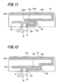
- FIG. 11 depicts according to another embodiment of the present disclosure a configuration of the electric power feeding element and a radiating element.
- the shape of the electric power feeding device 41 is a T shape. Contrary to the T-shaped power feeding element 41 of FIGS. 2, 5, 8 and 9 , the T-shaped power feeding element of FIG. 11 has an elongated right bar.
- the capacitive coupling formation element 422 of the radiating element 42 adjusts the capacitive value by lengthening the length of the front part 412 that comprises the right side of the T-shaped bar.
- the number of edges of the electric power feeding device 41 that is enclosed by the capacitive coupling formation part 422 are only three.
- the lower part, the upper part, and the right-end part of the right arm of the T-shaped power feeding element are enclosed.
- the base part of the power feeding element 411 and the left arm of the power feeding element 413 are not enclosed by the capacitive coupling part 422 .
- FIG. 12 illustrates according to another embodiment of the disclosure the configuration of the power feeding element 41 and the radiating element 422 .
- the power feeding element in FIG. 12 comprises of an elongated right arm of the T-shaped power feeding element 412 .
- the effective area S of the capacitive value is increased and thus the radiating element 422 encloses only two sides of the power feeding element 41 .
- the lower side of the right bar of the power feeding element 41 and the front end tip denoted by 412 are enclosed by the radiating element.
- the base part 411 and the front end of the left arm of the power feeding element 430 are not enclosed by the radiating element 422 .
- FIG. 13 depicts according to another embodiment of the present disclosure the configuration of the electric power feeding element and the radiating element.
- the electric power feeding element 41 is in the form of an L-shape, similar to the power feeding element of FIGS. 6 and 7 .
- the length of the L-shaped bar of the power feeding element 41 is considerably longer than that of FIGS. 6 and 7 .
- the number of edges (surfaces) that the electric power feeding element 41 is enclosed by the capacitive coupling formation element 422 is reduced. Specifically, only three sides need to be enclosed.
- the lower edge of 412 of the L-shaped bar, a part of the upper edge denoted by 422 e and the front tip of the L-shaped bar are enclosed by the capacitive coupling formation part 422 . Note that the base part 411 and the periphery of the front end tip of 412 are not enclosed by the capacitive coupling formation part 422 .
- FIG. 14 an alternate embodiment of the present disclosure illustrates the configuration of the electric power feeding element and the radiating element.
- the structure of the antenna system as depicted in FIG. 14 is similar to that as depicted in FIG. 13 .
- the length of the L-shaped bar in FIG. 14 is considerably longer than the L-shaped bar as depicted in FIG. 13 . This results in a reduction in the number of sides of the power feeding element 41 that need to be enclosed.
- the capacitive coupling formation part 422 of the radiating element 42 .
- the front tip 412 of the L-shaped bar and the bottom surface of the L-shaped bar are enclosed by the capacitive coupling formation.
- the base part 411 of the L-shaped bar of the radiating element is not enclosed by the capacitive formation unit 422 .
- FIGS. 15 and 16 depict the configuration of the electric power feeding element and the radiation element of the antenna system wherein two surfaces of the housing resin incorporate the radiating element and/or the capacitive coupling element.
- FIG. 15 illustrates in non-limiting example depicting a part of the radiation element being formed on the side surface ( 40 b ) of the housing resin 40 .
- a longitudinal arm 423 of the radiating element is formed on the surface 40 b of the housing resin 40 .
- the front part 412 and 413 and the capacitive coupling part 422 of the radiating element 42 are formed on the surface 40 s of the housing resin.
- FIG. 16 depicts a non-limiting example illustrating a part of the radiating element and a part of the capacitive coupling unit formed on the side surface of the housing resin.
- the front part 412 and 413 and the capacitive coupling part 422 of the radiating element 42 are found on the upper surface of the housing resin.
- a part of the capacitive coupling formation 422 are the terminals 412 e (the front end part of 412 of the electric power feeding device 41 ) and the terminals 413 e (the front part 413 of the electric power feeding device 41 ) are formed on the surface 40 s .
- the area between the top region of the electric power feeding element 41 and the capacitive coupling part 422 (denoted by Cp) is formed on the side surface of the housing resin.
- FIGS. 17 and 18 illustrate variations in the manner the capacitive coupling is formed between the radiating element and the electric power feed element.
- FIG. 17 illustrates a circularly shaped electric power feeding element.
- the shape of the electric power feeding is not restricted to an L-shaped or a T-shaped unit.
- the capacitive coupling part 422 of the radiating element is also made in a circular shape along the outer periphery of the front end 412 which is formed circularly.
- FIG. 18 illustrates an example wherein the radiation element is formed integrally with the capacitive coupling formation unit.
- the space between the radiation part 423 of the radiating element 42 and the capacitive coupling formation part 422 as depicted in FIG. 2 is filled with a metallic substance.
- the configuration of FIG. 18 is achieved.
- FIG. 19 depicts a non-limiting example illustrating the formation of a parasitic element 34 that is formed on the circuit board 30 .
- the parasitic element is formed by etching on a signal layer and connecting one end of the parasitic element to the ground layer 33 b . Note that this formation of the parasitic element by etching on the signal layer also functions as an antenna element.
- the electric power feeding element 41 and the radiating element 42 are formed on the housing resin 40 , which is on a layer different from the circuit board 30 , it is possible to position the parasitic element 34 three-dimensionally with respect to the feeding element 41 and radiating element 42 . This further provides flexibility in designing the antenna system.
- connection housing resin 40 that comprises the antenna element and the circuit board 30 is however not limited to a spring.
- a moveable probe pin such as a focal pin or an electroconductive metal shape or the like can be used.
- the electric feeding element and the radiating element may be formed as a pattern on a flexible printed circuit board and the flexible printed circuit board can be affixed on the housing resin 40 .
- the value of the capacitive coupling unit Cp in the present disclosure was assumed to be between 0.1 picofarad to 5 picofarad. However, this is not limiting the scope of the present invention and any other value may be set as the capacitive coupling value.
- the coupling adjustment element can comprise an inductor and a filter that pass/block a predetermined frequency band. Note that when the coupling adjustment element comprises a filter and an inductor, the filter is operated as in a capacitive nature at high frequencies and in an inductive nature at low frequencies. Specifically, since the coupling amount of the capacitive coupling part can be adjusted at the operating frequency bands of the antenna, the degree and freedom of designing further improves.
- the frequency bands that are passed/blocked by the antenna may include a plurality of filters and a switch that can select the operating frequency of the antenna by appropriately selecting the frequency pass bands.
- the capacity of the capacitive coupling part can be fully obtained by adjusting the length of the electric feeding unit 41 , it is not necessary to provide the coupling adjustment element.
- devices other than the mobile phone terminal device as described in the present disclosure may also be used to perform the features discussed in the present disclosure. For example, aspects of the present disclosure may be executed on a Smartphone, a tablet, or the like. The above disclosure also encompasses the embodiments noted below:
- An antenna comprising: a circuit board including a feed circuit and a ground terminal; a radiating element formed on a dielectric substrate positioned above the circuit board; a feed element formed on the dielectric substrate, the feed element disposed within an outer periphery defined by the radiating element; a first conductive element that connects the feed element to the feed circuit; and a second conductive element that connects the radiating element to the ground terminal.
- the antenna of (1) further comprising: a capacitive adjustment element formed on a transmission line that connects the feed circuit and the ground terminal.
- an effective capacitance of the antenna includes a first capacitance of the capacitive coupler and a second capacitance of the capacitive adjustment element.
- the antenna of (1) further comprises a parasitic element formed on the circuit board and connected at one end to the ground terminal.
- a terminal device comprising: a circuit board including a feed circuit and a ground terminal; an antenna unit including a radiating element formed on a dielectric substrate positioned above the circuit board; and a feed element formed on the dielectric substrate, the feed element disposed within an outer periphery defined by the radiating element; a first conductive element that connects the feed element to the feed circuit; and a second conductive element that connects the radiating element to the ground terminal.
Landscapes
- Engineering & Computer Science (AREA)
- Computer Networks & Wireless Communication (AREA)
- Physics & Mathematics (AREA)
- Electromagnetism (AREA)
- Support Of Aerials (AREA)
- Details Of Aerials (AREA)
Abstract
Description
wherein ∈ is the dielectric constant between the electric
C′=C+C2 (2)
Claims (20)
Priority Applications (1)
| Application Number | Priority Date | Filing Date | Title |
|---|---|---|---|
| US13/911,765 US9917357B2 (en) | 2013-06-06 | 2013-06-06 | Antenna system |
Applications Claiming Priority (1)
| Application Number | Priority Date | Filing Date | Title |
|---|---|---|---|
| US13/911,765 US9917357B2 (en) | 2013-06-06 | 2013-06-06 | Antenna system |
Publications (2)
| Publication Number | Publication Date |
|---|---|
| US20140361948A1 US20140361948A1 (en) | 2014-12-11 |
| US9917357B2 true US9917357B2 (en) | 2018-03-13 |
Family
ID=52005021
Family Applications (1)
| Application Number | Title | Priority Date | Filing Date |
|---|---|---|---|
| US13/911,765 Expired - Fee Related US9917357B2 (en) | 2013-06-06 | 2013-06-06 | Antenna system |
Country Status (1)
| Country | Link |
|---|---|
| US (1) | US9917357B2 (en) |
Cited By (2)
| Publication number | Priority date | Publication date | Assignee | Title |
|---|---|---|---|---|
| USD856984S1 (en) * | 2016-06-21 | 2019-08-20 | Redpine Signals, Inc. | Compact multi-band antenna |
| US20220399907A1 (en) * | 2021-06-11 | 2022-12-15 | Wistron Neweb Corp. | Antenna structure |
Families Citing this family (41)
| Publication number | Priority date | Publication date | Assignee | Title |
|---|---|---|---|---|
| KR101918990B1 (en) * | 2012-05-09 | 2018-11-16 | 엘지전자 주식회사 | Antenna apparatus and mobile terminal having the same |
| TWI462393B (en) * | 2013-10-04 | 2014-11-21 | Wistron Neweb Corp | Antenna |
| CN104733861A (en) * | 2013-12-20 | 2015-06-24 | 深圳富泰宏精密工业有限公司 | Antenna structure and wireless communication device with same |
| US9406996B2 (en) | 2014-01-22 | 2016-08-02 | Agc Automotive Americas R&D, Inc. | Window assembly with transparent layer and an antenna element |
| USD747298S1 (en) * | 2014-01-22 | 2016-01-12 | Agc Automotive Americas R&D, Inc. | Antenna |
| USD774024S1 (en) * | 2014-01-22 | 2016-12-13 | Agc Automotive Americas R&D, Inc. | Antenna |
| US9806398B2 (en) | 2014-01-22 | 2017-10-31 | Agc Automotive Americas R&D, Inc. | Window assembly with transparent layer and an antenna element |
| USD788078S1 (en) | 2014-01-22 | 2017-05-30 | Agc Automotive Americas R&D, Inc. | Antenna |
| JP2015170961A (en) * | 2014-03-06 | 2015-09-28 | ホシデン株式会社 | Antenna device, transmission module using antenna device, and position identification system using transmission module |
| TWI533516B (en) * | 2014-04-07 | 2016-05-11 | 啟碁科技股份有限公司 | Switchable antenna |
| CN105633549B (en) * | 2014-10-31 | 2020-06-19 | 深圳富泰宏精密工业有限公司 | Antenna structure and wireless communication device using the same |
| US9437926B2 (en) * | 2014-12-01 | 2016-09-06 | Wistron Corporation | Antenna having asymmetric T shape coupled feed |
| US10622702B2 (en) * | 2014-12-26 | 2020-04-14 | Byd Company Limited | Mobile terminal and antenna of mobile terminal |
| CN204391262U (en) * | 2015-01-20 | 2015-06-10 | 瑞声精密制造科技(常州)有限公司 | Anneta module |
| TWI662741B (en) * | 2015-01-23 | 2019-06-11 | 群邁通訊股份有限公司 | Antenna structure and wireless communication device having the same |
| WO2017058178A1 (en) * | 2015-09-29 | 2017-04-06 | Hewlett-Packard Development Company, L.P. | Ground excitation antennas |
| US10637147B2 (en) | 2015-09-29 | 2020-04-28 | Hewlett-Packard Development Company, L.P. | Wideband antennas |
| WO2017142550A1 (en) * | 2016-02-19 | 2017-08-24 | Hewlett-Packard Development Company, L.P. | Integrated antenna |
| CN107579334A (en) * | 2016-07-05 | 2018-01-12 | 宏碁股份有限公司 | mobile device |
| CN112002993B (en) * | 2016-11-29 | 2023-09-19 | 株式会社村田制作所 | Antenna devices and electronic equipment |
| TWI630754B (en) * | 2016-12-09 | 2018-07-21 | 群邁通訊股份有限公司 | Antenna structure and wireless communication device with same |
| CN108270075A (en) * | 2016-12-30 | 2018-07-10 | 鸿富锦精密电子(郑州)有限公司 | The electronic device of multiband antenna and the application antenna |
| NL2018147B1 (en) * | 2017-01-09 | 2018-07-25 | The Antenna Company International N V | GNSS antenna, GNSS module, and vehicle having such a GNSS module |
| CN108963444B (en) * | 2017-05-27 | 2021-03-26 | 国基电子(上海)有限公司 | Antenna, energy conversion and communication system |
| TWI663777B (en) | 2017-08-02 | 2019-06-21 | 啟碁科技股份有限公司 | Antenna structure |
| TWI638486B (en) * | 2017-10-27 | 2018-10-11 | 廣達電腦股份有限公司 | Mobile device |
| TWI672860B (en) * | 2018-08-24 | 2019-09-21 | 宏碁股份有限公司 | Electronic device |
| CN109841943B (en) * | 2019-03-01 | 2024-03-19 | 深圳市信维通信股份有限公司 | Three-frequency MIMO antenna system applied to 5G communication and mobile terminal |
| WO2021000071A1 (en) * | 2019-06-29 | 2021-01-07 | 瑞声声学科技(深圳)有限公司 | Antenna module and mobile terminal |
| TWI704718B (en) * | 2019-07-12 | 2020-09-11 | 啟碁科技股份有限公司 | Antenna structure |
| TWI712218B (en) * | 2019-11-28 | 2020-12-01 | 廣達電腦股份有限公司 | Antenna structure |
| TWI723833B (en) * | 2020-04-01 | 2021-04-01 | 啟碁科技股份有限公司 | Antenna structure |
| TWI736285B (en) * | 2020-05-25 | 2021-08-11 | 宏碁股份有限公司 | Antenna structure |
| TWI768865B (en) * | 2021-05-03 | 2022-06-21 | 和碩聯合科技股份有限公司 | Antenna module and electronic device |
| TWI788038B (en) * | 2021-10-04 | 2022-12-21 | 啟碁科技股份有限公司 | Electronic device |
| EP4418455A4 (en) * | 2021-11-17 | 2025-03-05 | Samsung Electronics Co., Ltd. | Antenna and electronic apparatus comprising same |
| TWI823597B (en) * | 2022-10-04 | 2023-11-21 | 華碩電腦股份有限公司 | Coupled-feed multi-branch antenna system |
| TWI839953B (en) * | 2022-11-21 | 2024-04-21 | 緯創資通股份有限公司 | Antenna module |
| TWI882481B (en) * | 2023-10-19 | 2025-05-01 | 啟碁科技股份有限公司 | Electronic device and antenna structure |
| TWI883628B (en) * | 2023-11-03 | 2025-05-11 | 和碩聯合科技股份有限公司 | Antenna module |
| TWM654049U (en) * | 2023-11-29 | 2024-04-11 | 廣達電腦股份有限公司 | Antenna structure |
Citations (11)
| Publication number | Priority date | Publication date | Assignee | Title |
|---|---|---|---|---|
| US5764189A (en) * | 1995-09-27 | 1998-06-09 | Siemens Aktiengesellschaft | Doppler radar module |
| US5874926A (en) * | 1996-03-11 | 1999-02-23 | Murata Mfg Co. Ltd | Matching circuit and antenna apparatus |
| US6469590B1 (en) * | 2000-06-20 | 2002-10-22 | Shakespeare Company | Marine antenna with an integral filter |
| US20070262906A1 (en) * | 2006-05-11 | 2007-11-15 | Yona Haim | Capacitive ground antenna |
| US7301502B2 (en) | 2005-08-18 | 2007-11-27 | Nokia Corporation | Antenna arrangement for a cellular communication terminal |
| US7602341B2 (en) * | 2007-01-25 | 2009-10-13 | Wistron Neweb Corp. | Multi-band antenna |
| US7825863B2 (en) * | 2006-11-16 | 2010-11-02 | Galtronics Ltd. | Compact antenna |
| US7932865B2 (en) | 2008-05-05 | 2011-04-26 | Acer Incorporated | Coplanar coupled-fed multiband antenna for the mobile device |
| US7990321B2 (en) | 2009-01-16 | 2011-08-02 | Hon Hai Precision Industry Co., Ltd. | Multiband antenna |
| US20110298669A1 (en) * | 2010-06-08 | 2011-12-08 | Research In Motion Limited | Low frequency dual-antenna diversity system |
| US9007266B2 (en) * | 2007-07-30 | 2015-04-14 | Htc Corporation | Receiving device for global positioning system and antenna structure thereof |
-
2013
- 2013-06-06 US US13/911,765 patent/US9917357B2/en not_active Expired - Fee Related
Patent Citations (11)
| Publication number | Priority date | Publication date | Assignee | Title |
|---|---|---|---|---|
| US5764189A (en) * | 1995-09-27 | 1998-06-09 | Siemens Aktiengesellschaft | Doppler radar module |
| US5874926A (en) * | 1996-03-11 | 1999-02-23 | Murata Mfg Co. Ltd | Matching circuit and antenna apparatus |
| US6469590B1 (en) * | 2000-06-20 | 2002-10-22 | Shakespeare Company | Marine antenna with an integral filter |
| US7301502B2 (en) | 2005-08-18 | 2007-11-27 | Nokia Corporation | Antenna arrangement for a cellular communication terminal |
| US20070262906A1 (en) * | 2006-05-11 | 2007-11-15 | Yona Haim | Capacitive ground antenna |
| US7825863B2 (en) * | 2006-11-16 | 2010-11-02 | Galtronics Ltd. | Compact antenna |
| US7602341B2 (en) * | 2007-01-25 | 2009-10-13 | Wistron Neweb Corp. | Multi-band antenna |
| US9007266B2 (en) * | 2007-07-30 | 2015-04-14 | Htc Corporation | Receiving device for global positioning system and antenna structure thereof |
| US7932865B2 (en) | 2008-05-05 | 2011-04-26 | Acer Incorporated | Coplanar coupled-fed multiband antenna for the mobile device |
| US7990321B2 (en) | 2009-01-16 | 2011-08-02 | Hon Hai Precision Industry Co., Ltd. | Multiband antenna |
| US20110298669A1 (en) * | 2010-06-08 | 2011-12-08 | Research In Motion Limited | Low frequency dual-antenna diversity system |
Cited By (3)
| Publication number | Priority date | Publication date | Assignee | Title |
|---|---|---|---|---|
| USD856984S1 (en) * | 2016-06-21 | 2019-08-20 | Redpine Signals, Inc. | Compact multi-band antenna |
| US20220399907A1 (en) * | 2021-06-11 | 2022-12-15 | Wistron Neweb Corp. | Antenna structure |
| US11824568B2 (en) * | 2021-06-11 | 2023-11-21 | Wistron Neweb Corp. | Antenna structure |
Also Published As
| Publication number | Publication date |
|---|---|
| US20140361948A1 (en) | 2014-12-11 |
Similar Documents
| Publication | Publication Date | Title |
|---|---|---|
| US9917357B2 (en) | Antenna system | |
| KR102162343B1 (en) | Electronic device wide band antennas | |
| AU2015101429B4 (en) | Electronic device cavity antennas with slots and monopoles | |
| US10218052B2 (en) | Electronic device with tunable hybrid antennas | |
| US9059520B2 (en) | Wireless communication device and communication terminal apparatus | |
| EP2507866B1 (en) | Bezel antenna | |
| US7525488B2 (en) | Meander feed structure antenna systems and methods | |
| JP6490080B2 (en) | Technology to adjust antenna by weak coupling of variable impedance element | |
| EP2418728A1 (en) | Antenna arrangement, dielectric substrate, PCB & device | |
| KR101700744B1 (en) | Built-in antenna for portable terminal | |
| US10141637B2 (en) | Pattern antenna | |
| JP6015944B2 (en) | ANTENNA DEVICE, COMMUNICATION DEVICE, AND ELECTRONIC DEVICE | |
| AU2014200229B2 (en) | Antenna and mobile terminal having the same | |
| US11742580B2 (en) | Multifeed antenna system with capacitively coupled feed elements | |
| US9306274B2 (en) | Antenna device and antenna mounting method | |
| US20120115336A1 (en) | Slide-type wireless terminal apparatus | |
| WO2011103710A1 (en) | An antenna arrangement for covering a frequency band | |
| US9570800B2 (en) | Ground antenna and ground radiator using capacitor | |
| EP2341578A1 (en) | Chip antenna | |
| JP6865072B2 (en) | Antenna device and electronic device equipped with an antenna device | |
| JP2012095121A (en) | Antenna and portable radio device | |
| CN111384588B (en) | Multi-frequency antenna | |
| US11342670B1 (en) | Antenna structure | |
| KR20120029988A (en) | Antenna apparatus for portable terminal | |
| HK40068144A (en) | Multifeed antenna system with capacitively coupled feed elements |
Legal Events
| Date | Code | Title | Description |
|---|---|---|---|
| AS | Assignment |
Owner name: SONY CORPORATION, JAPAN Free format text: ASSIGNMENT OF ASSIGNORS INTEREST;ASSIGNORS:TANAKA, MASATO;SHOJI, HIDEAKI;YOSHIDA, AIKO;SIGNING DATES FROM 20141022 TO 20141023;REEL/FRAME:034129/0786 |
|
| AS | Assignment |
Owner name: SONY MOBILE COMMUNICATIONS INC., JAPAN Free format text: ASSIGNMENT OF PARTIAL RIGHTS;ASSIGNOR:SONY CORPORATION;REEL/FRAME:044836/0490 Effective date: 20171102 |
|
| STCF | Information on status: patent grant |
Free format text: PATENTED CASE |
|
| AS | Assignment |
Owner name: SONY CORPORATION, JAPAN Free format text: ASSIGNMENT OF ASSIGNORS INTEREST;ASSIGNOR:SONY MOBILE COMMUNICATIONS, INC.;REEL/FRAME:049404/0887 Effective date: 20190325 |
|
| MAFP | Maintenance fee payment |
Free format text: PAYMENT OF MAINTENANCE FEE, 4TH YEAR, LARGE ENTITY (ORIGINAL EVENT CODE: M1551); ENTITY STATUS OF PATENT OWNER: LARGE ENTITY Year of fee payment: 4 |
|
| FEPP | Fee payment procedure |
Free format text: MAINTENANCE FEE REMINDER MAILED (ORIGINAL EVENT CODE: REM.); ENTITY STATUS OF PATENT OWNER: LARGE ENTITY |
|
| LAPS | Lapse for failure to pay maintenance fees |
Free format text: PATENT EXPIRED FOR FAILURE TO PAY MAINTENANCE FEES (ORIGINAL EVENT CODE: EXP.); ENTITY STATUS OF PATENT OWNER: LARGE ENTITY |
|
| STCH | Information on status: patent discontinuation |
Free format text: PATENT EXPIRED DUE TO NONPAYMENT OF MAINTENANCE FEES UNDER 37 CFR 1.362 |