US9916266B2 - High performance interconnect physical layer - Google Patents
High performance interconnect physical layer Download PDFInfo
- Publication number
- US9916266B2 US9916266B2 US15/237,291 US201615237291A US9916266B2 US 9916266 B2 US9916266 B2 US 9916266B2 US 201615237291 A US201615237291 A US 201615237291A US 9916266 B2 US9916266 B2 US 9916266B2
- Authority
- US
- United States
- Prior art keywords
- state
- detect
- link
- processor
- supersequence
- Prior art date
- Legal status (The legal status is an assumption and is not a legal conclusion. Google has not performed a legal analysis and makes no representation as to the accuracy of the status listed.)
- Active
Links
Images


Classifications
-
- G—PHYSICS
- G06—COMPUTING; CALCULATING OR COUNTING
- G06F—ELECTRIC DIGITAL DATA PROCESSING
- G06F13/00—Interconnection of, or transfer of information or other signals between, memories, input/output devices or central processing units
- G06F13/14—Handling requests for interconnection or transfer
- G06F13/20—Handling requests for interconnection or transfer for access to input/output bus
- G06F13/22—Handling requests for interconnection or transfer for access to input/output bus using successive scanning, e.g. polling
-
- G—PHYSICS
- G06—COMPUTING; CALCULATING OR COUNTING
- G06F—ELECTRIC DIGITAL DATA PROCESSING
- G06F1/00—Details not covered by groups G06F3/00 - G06F13/00 and G06F21/00
- G06F1/26—Power supply means, e.g. regulation thereof
- G06F1/32—Means for saving power
- G06F1/3203—Power management, i.e. event-based initiation of a power-saving mode
- G06F1/3234—Power saving characterised by the action undertaken
- G06F1/3287—Power saving characterised by the action undertaken by switching off individual functional units in the computer system
-
- G—PHYSICS
- G06—COMPUTING; CALCULATING OR COUNTING
- G06F—ELECTRIC DIGITAL DATA PROCESSING
- G06F11/00—Error detection; Error correction; Monitoring
- G06F11/07—Responding to the occurrence of a fault, e.g. fault tolerance
- G06F11/08—Error detection or correction by redundancy in data representation, e.g. by using checking codes
- G06F11/10—Adding special bits or symbols to the coded information, e.g. parity check, casting out 9's or 11's
- G06F11/1004—Adding special bits or symbols to the coded information, e.g. parity check, casting out 9's or 11's to protect a block of data words, e.g. CRC or checksum
-
- G—PHYSICS
- G06—COMPUTING; CALCULATING OR COUNTING
- G06F—ELECTRIC DIGITAL DATA PROCESSING
- G06F12/00—Accessing, addressing or allocating within memory systems or architectures
- G06F12/02—Addressing or allocation; Relocation
- G06F12/08—Addressing or allocation; Relocation in hierarchically structured memory systems, e.g. virtual memory systems
- G06F12/0802—Addressing of a memory level in which the access to the desired data or data block requires associative addressing means, e.g. caches
- G06F12/0806—Multiuser, multiprocessor or multiprocessing cache systems
- G06F12/0808—Multiuser, multiprocessor or multiprocessing cache systems with cache invalidating means
-
- G—PHYSICS
- G06—COMPUTING; CALCULATING OR COUNTING
- G06F—ELECTRIC DIGITAL DATA PROCESSING
- G06F12/00—Accessing, addressing or allocating within memory systems or architectures
- G06F12/02—Addressing or allocation; Relocation
- G06F12/08—Addressing or allocation; Relocation in hierarchically structured memory systems, e.g. virtual memory systems
- G06F12/0802—Addressing of a memory level in which the access to the desired data or data block requires associative addressing means, e.g. caches
- G06F12/0806—Multiuser, multiprocessor or multiprocessing cache systems
- G06F12/0813—Multiuser, multiprocessor or multiprocessing cache systems with a network or matrix configuration
-
- G—PHYSICS
- G06—COMPUTING; CALCULATING OR COUNTING
- G06F—ELECTRIC DIGITAL DATA PROCESSING
- G06F12/00—Accessing, addressing or allocating within memory systems or architectures
- G06F12/02—Addressing or allocation; Relocation
- G06F12/08—Addressing or allocation; Relocation in hierarchically structured memory systems, e.g. virtual memory systems
- G06F12/0802—Addressing of a memory level in which the access to the desired data or data block requires associative addressing means, e.g. caches
- G06F12/0806—Multiuser, multiprocessor or multiprocessing cache systems
- G06F12/0815—Cache consistency protocols
- G06F12/0831—Cache consistency protocols using a bus scheme, e.g. with bus monitoring or watching means
- G06F12/0833—Cache consistency protocols using a bus scheme, e.g. with bus monitoring or watching means in combination with broadcast means (e.g. for invalidation or updating)
-
- G—PHYSICS
- G06—COMPUTING; CALCULATING OR COUNTING
- G06F—ELECTRIC DIGITAL DATA PROCESSING
- G06F13/00—Interconnection of, or transfer of information or other signals between, memories, input/output devices or central processing units
- G06F13/14—Handling requests for interconnection or transfer
- G06F13/16—Handling requests for interconnection or transfer for access to memory bus
- G06F13/1605—Handling requests for interconnection or transfer for access to memory bus based on arbitration
- G06F13/1652—Handling requests for interconnection or transfer for access to memory bus based on arbitration in a multiprocessor architecture
- G06F13/1657—Access to multiple memories
-
- G—PHYSICS
- G06—COMPUTING; CALCULATING OR COUNTING
- G06F—ELECTRIC DIGITAL DATA PROCESSING
- G06F13/00—Interconnection of, or transfer of information or other signals between, memories, input/output devices or central processing units
- G06F13/14—Handling requests for interconnection or transfer
- G06F13/16—Handling requests for interconnection or transfer for access to memory bus
- G06F13/1668—Details of memory controller
- G06F13/1689—Synchronisation and timing concerns
-
- G—PHYSICS
- G06—COMPUTING; CALCULATING OR COUNTING
- G06F—ELECTRIC DIGITAL DATA PROCESSING
- G06F13/00—Interconnection of, or transfer of information or other signals between, memories, input/output devices or central processing units
- G06F13/38—Information transfer, e.g. on bus
- G06F13/40—Bus structure
- G06F13/4063—Device-to-bus coupling
- G06F13/4068—Electrical coupling
-
- G—PHYSICS
- G06—COMPUTING; CALCULATING OR COUNTING
- G06F—ELECTRIC DIGITAL DATA PROCESSING
- G06F13/00—Interconnection of, or transfer of information or other signals between, memories, input/output devices or central processing units
- G06F13/38—Information transfer, e.g. on bus
- G06F13/42—Bus transfer protocol, e.g. handshake; Synchronisation
- G06F13/4204—Bus transfer protocol, e.g. handshake; Synchronisation on a parallel bus
- G06F13/4221—Bus transfer protocol, e.g. handshake; Synchronisation on a parallel bus being an input/output bus, e.g. ISA bus, EISA bus, PCI bus, SCSI bus
-
- G—PHYSICS
- G06—COMPUTING; CALCULATING OR COUNTING
- G06F—ELECTRIC DIGITAL DATA PROCESSING
- G06F13/00—Interconnection of, or transfer of information or other signals between, memories, input/output devices or central processing units
- G06F13/38—Information transfer, e.g. on bus
- G06F13/42—Bus transfer protocol, e.g. handshake; Synchronisation
- G06F13/4282—Bus transfer protocol, e.g. handshake; Synchronisation on a serial bus, e.g. I2C bus, SPI bus
- G06F13/4286—Bus transfer protocol, e.g. handshake; Synchronisation on a serial bus, e.g. I2C bus, SPI bus using a handshaking protocol, e.g. RS232C link
-
- G—PHYSICS
- G06—COMPUTING; CALCULATING OR COUNTING
- G06F—ELECTRIC DIGITAL DATA PROCESSING
- G06F13/00—Interconnection of, or transfer of information or other signals between, memories, input/output devices or central processing units
- G06F13/38—Information transfer, e.g. on bus
- G06F13/42—Bus transfer protocol, e.g. handshake; Synchronisation
- G06F13/4282—Bus transfer protocol, e.g. handshake; Synchronisation on a serial bus, e.g. I2C bus, SPI bus
- G06F13/4291—Bus transfer protocol, e.g. handshake; Synchronisation on a serial bus, e.g. I2C bus, SPI bus using a clocked protocol
-
- G—PHYSICS
- G06—COMPUTING; CALCULATING OR COUNTING
- G06F—ELECTRIC DIGITAL DATA PROCESSING
- G06F8/00—Arrangements for software engineering
- G06F8/70—Software maintenance or management
- G06F8/71—Version control; Configuration management
-
- G—PHYSICS
- G06—COMPUTING; CALCULATING OR COUNTING
- G06F—ELECTRIC DIGITAL DATA PROCESSING
- G06F8/00—Arrangements for software engineering
- G06F8/70—Software maintenance or management
- G06F8/77—Software metrics
-
- G—PHYSICS
- G06—COMPUTING; CALCULATING OR COUNTING
- G06F—ELECTRIC DIGITAL DATA PROCESSING
- G06F9/00—Arrangements for program control, e.g. control units
- G06F9/06—Arrangements for program control, e.g. control units using stored programs, i.e. using an internal store of processing equipment to receive or retain programs
- G06F9/30—Arrangements for executing machine instructions, e.g. instruction decode
- G06F9/30145—Instruction analysis, e.g. decoding, instruction word fields
-
- G—PHYSICS
- G06—COMPUTING; CALCULATING OR COUNTING
- G06F—ELECTRIC DIGITAL DATA PROCESSING
- G06F9/00—Arrangements for program control, e.g. control units
- G06F9/06—Arrangements for program control, e.g. control units using stored programs, i.e. using an internal store of processing equipment to receive or retain programs
- G06F9/44—Arrangements for executing specific programs
- G06F9/445—Program loading or initiating
- G06F9/44505—Configuring for program initiating, e.g. using registry, configuration files
-
- G—PHYSICS
- G06—COMPUTING; CALCULATING OR COUNTING
- G06F—ELECTRIC DIGITAL DATA PROCESSING
- G06F9/00—Arrangements for program control, e.g. control units
- G06F9/06—Arrangements for program control, e.g. control units using stored programs, i.e. using an internal store of processing equipment to receive or retain programs
- G06F9/46—Multiprogramming arrangements
- G06F9/466—Transaction processing
-
- H—ELECTRICITY
- H04—ELECTRIC COMMUNICATION TECHNIQUE
- H04L—TRANSMISSION OF DIGITAL INFORMATION, e.g. TELEGRAPHIC COMMUNICATION
- H04L12/00—Data switching networks
- H04L12/54—Store-and-forward switching systems
- H04L12/56—Packet switching systems
-
- H—ELECTRICITY
- H04—ELECTRIC COMMUNICATION TECHNIQUE
- H04L—TRANSMISSION OF DIGITAL INFORMATION, e.g. TELEGRAPHIC COMMUNICATION
- H04L49/00—Packet switching elements
- H04L49/15—Interconnection of switching modules
-
- H—ELECTRICITY
- H04—ELECTRIC COMMUNICATION TECHNIQUE
- H04L—TRANSMISSION OF DIGITAL INFORMATION, e.g. TELEGRAPHIC COMMUNICATION
- H04L9/00—Cryptographic mechanisms or cryptographic arrangements for secret or secure communications; Network security protocols
- H04L9/06—Cryptographic mechanisms or cryptographic arrangements for secret or secure communications; Network security protocols the encryption apparatus using shift registers or memories for block-wise or stream coding, e.g. DES systems or RC4; Hash functions; Pseudorandom sequence generators
- H04L9/065—Encryption by serially and continuously modifying data stream elements, e.g. stream cipher systems, RC4, SEAL or A5/3
- H04L9/0656—Pseudorandom key sequence combined element-for-element with data sequence, e.g. one-time-pad [OTP] or Vernam's cipher
- H04L9/0662—Pseudorandom key sequence combined element-for-element with data sequence, e.g. one-time-pad [OTP] or Vernam's cipher with particular pseudorandom sequence generator
-
- G—PHYSICS
- G06—COMPUTING; CALCULATING OR COUNTING
- G06F—ELECTRIC DIGITAL DATA PROCESSING
- G06F13/00—Interconnection of, or transfer of information or other signals between, memories, input/output devices or central processing units
- G06F13/38—Information transfer, e.g. on bus
- G06F13/40—Bus structure
- G06F13/4004—Coupling between buses
- G06F13/4022—Coupling between buses using switching circuits, e.g. switching matrix, connection or expansion network
-
- G—PHYSICS
- G06—COMPUTING; CALCULATING OR COUNTING
- G06F—ELECTRIC DIGITAL DATA PROCESSING
- G06F13/00—Interconnection of, or transfer of information or other signals between, memories, input/output devices or central processing units
- G06F13/38—Information transfer, e.g. on bus
- G06F13/42—Bus transfer protocol, e.g. handshake; Synchronisation
- G06F13/4265—Bus transfer protocol, e.g. handshake; Synchronisation on a point to point bus
- G06F13/4273—Bus transfer protocol, e.g. handshake; Synchronisation on a point to point bus using a clocked protocol
-
- G—PHYSICS
- G06—COMPUTING; CALCULATING OR COUNTING
- G06F—ELECTRIC DIGITAL DATA PROCESSING
- G06F2212/00—Indexing scheme relating to accessing, addressing or allocation within memory systems or architectures
- G06F2212/10—Providing a specific technical effect
- G06F2212/1016—Performance improvement
-
- G—PHYSICS
- G06—COMPUTING; CALCULATING OR COUNTING
- G06F—ELECTRIC DIGITAL DATA PROCESSING
- G06F2212/00—Indexing scheme relating to accessing, addressing or allocation within memory systems or architectures
- G06F2212/25—Using a specific main memory architecture
- G06F2212/254—Distributed memory
- G06F2212/2542—Non-uniform memory access [NUMA] architecture
-
- G—PHYSICS
- G06—COMPUTING; CALCULATING OR COUNTING
- G06F—ELECTRIC DIGITAL DATA PROCESSING
- G06F2212/00—Indexing scheme relating to accessing, addressing or allocation within memory systems or architectures
- G06F2212/62—Details of cache specific to multiprocessor cache arrangements
- G06F2212/622—State-only directory, i.e. not recording identity of sharing or owning nodes
-
- G—PHYSICS
- G06—COMPUTING; CALCULATING OR COUNTING
- G06F—ELECTRIC DIGITAL DATA PROCESSING
- G06F8/00—Arrangements for software engineering
- G06F8/70—Software maintenance or management
- G06F8/73—Program documentation
-
- H—ELECTRICITY
- H04—ELECTRIC COMMUNICATION TECHNIQUE
- H04L—TRANSMISSION OF DIGITAL INFORMATION, e.g. TELEGRAPHIC COMMUNICATION
- H04L12/00—Data switching networks
- H04L12/28—Data switching networks characterised by path configuration, e.g. LAN [Local Area Networks] or WAN [Wide Area Networks]
- H04L12/46—Interconnection of networks
- H04L12/4641—Virtual LANs, VLANs, e.g. virtual private networks [VPN]
-
- H—ELECTRICITY
- H04—ELECTRIC COMMUNICATION TECHNIQUE
- H04L—TRANSMISSION OF DIGITAL INFORMATION, e.g. TELEGRAPHIC COMMUNICATION
- H04L45/00—Routing or path finding of packets in data switching networks
- H04L45/74—Address processing for routing
-
- Y—GENERAL TAGGING OF NEW TECHNOLOGICAL DEVELOPMENTS; GENERAL TAGGING OF CROSS-SECTIONAL TECHNOLOGIES SPANNING OVER SEVERAL SECTIONS OF THE IPC; TECHNICAL SUBJECTS COVERED BY FORMER USPC CROSS-REFERENCE ART COLLECTIONS [XRACs] AND DIGESTS
- Y02—TECHNOLOGIES OR APPLICATIONS FOR MITIGATION OR ADAPTATION AGAINST CLIMATE CHANGE
- Y02D—CLIMATE CHANGE MITIGATION TECHNOLOGIES IN INFORMATION AND COMMUNICATION TECHNOLOGIES [ICT], I.E. INFORMATION AND COMMUNICATION TECHNOLOGIES AIMING AT THE REDUCTION OF THEIR OWN ENERGY USE
- Y02D10/00—Energy efficient computing, e.g. low power processors, power management or thermal management
-
- Y—GENERAL TAGGING OF NEW TECHNOLOGICAL DEVELOPMENTS; GENERAL TAGGING OF CROSS-SECTIONAL TECHNOLOGIES SPANNING OVER SEVERAL SECTIONS OF THE IPC; TECHNICAL SUBJECTS COVERED BY FORMER USPC CROSS-REFERENCE ART COLLECTIONS [XRACs] AND DIGESTS
- Y02—TECHNOLOGIES OR APPLICATIONS FOR MITIGATION OR ADAPTATION AGAINST CLIMATE CHANGE
- Y02D—CLIMATE CHANGE MITIGATION TECHNOLOGIES IN INFORMATION AND COMMUNICATION TECHNOLOGIES [ICT], I.E. INFORMATION AND COMMUNICATION TECHNOLOGIES AIMING AT THE REDUCTION OF THEIR OWN ENERGY USE
- Y02D30/00—Reducing energy consumption in communication networks
Definitions
- the present disclosure relates in general to the field of computer development, and more specifically, to software development involving coordination of mutually-dependent constrained systems.
- a processor or integrated circuit typically comprises a single physical processor die, where the processor die may include any number of cores, hardware threads, logical processors, interfaces, memory, controller hubs, etc.
- interconnects have grown from more traditional multi-drop buses that primarily handled electrical communications to full blown interconnect architectures that facilitate fast communication.
- FIG. 1 illustrates a simplified block diagram of a system including a serial point-to-point interconnect to connect I/O devices in a computer system in accordance with one embodiment
- FIG. 2 illustrates a simplified block diagram of a layered protocol stack in accordance with one embodiment
- FIG. 3 illustrates an embodiment of a transaction descriptor.
- FIG. 4 illustrates an embodiment of a serial point-to-point link.
- FIG. 5 illustrates embodiments of potential High Performance Interconnect (HPI) system configurations.
- HPI High Performance Interconnect
- FIG. 6 illustrates an embodiment of a layered protocol stack associated with HPI.
- FIG. 7 illustrates a representation of an example state machine.
- FIG. 8 illustrates example control supersequences.
- FIG. 9 illustrates a flow diagram of an example transition to a partial width state.
- FIG. 10 illustrates an embodiment of a block diagram for a computing system including a multicore processor.
- FIG. 11 illustrates another embodiment of a block diagram for a computing system including a multicore processor.
- FIG. 12 illustrates an embodiment of a block diagram for a processor.
- FIG. 13 illustrates another embodiment of a block diagram for a computing system including a processor.
- FIG. 14 illustrates an embodiment of a block for a computing system including multiple processor sockets.
- FIG. 15 illustrates another embodiment of a block diagram for a computing system.
- the disclosed embodiments are not limited to server computer system, desktop computer systems, laptops, UltrabooksTM, but may be also used in other devices, such as handheld devices, smartphones, tablets, other thin notebooks, systems on a chip (SOC) devices, and embedded applications.
- handheld devices include cellular phones, Internet protocol devices, digital cameras, personal digital assistants (PDAs), and handheld PCs.
- Embedded applications typically include a microcontroller, a digital signal processor (DSP), a system on a chip, network computers (NetPC), set-top boxes, network hubs, wide area network (WAN) switches, or any other system that can perform the functions and operations taught below.
- DSP digital signal processor
- NetPC network computers
- Set-top boxes network hubs
- WAN wide area network
- the apparatus', methods, and systems described herein are not limited to physical computing devices, but may also relate to software optimizations for energy conservation and efficiency. As may become readily apparent in the description below, the embodiments of methods, apparatus', and systems described herein (whether in reference to hardware, firmware, software, or a combination thereof) may be considered vital to a “green technology” future balanced with performance considerations.
- interconnect architecture to couple and communicate between the components has also increased in complexity to ensure bandwidth demand is met for optimal component operation.
- different market segments demand different aspects of interconnect architectures to suit the respective market. For example, servers require higher performance, while the mobile ecosystem is sometimes able to sacrifice overall performance for power savings. Yet, it is a singular purpose of most fabrics to provide highest possible performance with maximum power saving. Further, a variety of different interconnects can potentially benefit from subject matter described herein.
- PCIe Peripheral Component Interconnect Express
- QPI QuickPath Interconnect
- PCIe Peripheral Component Interconnect Express
- PCIe Peripheral Component Interconnect Express
- QPI QuickPath Interconnect
- PCIe Peripheral Component Interconnect Express
- a primary goal of PCIe is to enable components and devices from different vendors to inter-operate in an open architecture, spanning multiple market segments; Clients (Desktops and Mobile), Servers (Standard and Enterprise), and Embedded and Communication devices.
- PCI Express is a high performance, general purpose I/O interconnect defined for a wide variety of future computing and communication platforms.
- PCI attributes such as its usage model, load-store architecture, and software interfaces
- PCI Express Some PCI attributes, such as its usage model, load-store architecture, and software interfaces, have been maintained through its revisions, whereas previous parallel bus implementations have been replaced by a highly scalable, fully serial interface.
- the more recent versions of PCI Express take advantage of advances in point-to-point interconnects, Switch-based technology, and packetized protocol to deliver new levels of performance and features. Power Management, Quality Of Service (QoS), Hot-Plug/Hot-Swap support, Data Integrity, and Error Handling are among some of the advanced features supported by PCI Express.
- QoS Quality Of Service
- Hot-Plug/Hot-Swap support Data Integrity
- Error Handling are among some of the advanced features supported by PCI Express.
- HPI high-performance interconnect
- aspects of the invention described herein may be applied to other interconnect architectures, such as a PCIe-compliant architecture, a QPI-compliant architecture, a MIPI compliant architecture, a high-performance architecture, or other known interconnect architecture.
- System 100 includes processor 105 and system memory 110 coupled to controller hub 115 .
- Processor 105 can include any processing element, such as a microprocessor, a host processor, an embedded processor, a co-processor, or other processor.
- Processor 105 is coupled to controller hub 115 through front-side bus (FSB) 106 .
- FSB 106 is a serial point-to-point interconnect as described below.
- link 106 includes a serial, differential interconnect architecture that is compliant with different interconnect standard.
- System memory 110 includes any memory device, such as random access memory (RAM), non-volatile (NV) memory, or other memory accessible by devices in system 100 .
- System memory 110 is coupled to controller hub 115 through memory interface 116 .
- Examples of a memory interface include a double-data rate (DDR) memory interface, a dual-channel DDR memory interface, and a dynamic RAM (DRAM) memory interface.
- DDR double-data rate
- DRAM dynamic RAM
- controller hub 115 can include a root hub, root complex, or root controller, such as in a PCIc interconnection hierarchy.
- controller hub 115 include a chipset, a memory controller hub (MCH), a northbridge, an interconnect controller hub (ICH) a southbridge, and a root controller/hub.
- chipset refers to two physically separate controller hubs, e.g., a memory controller hub (MCH) coupled to an interconnect controller hub (ICH).
- MCH memory controller hub
- ICH interconnect controller hub
- ICH interconnect controller hub
- current systems often include the MCH integrated with processor 105 , while controller 115 is to communicate with I/O devices, in a similar manner as described below.
- peer-to-peer routing is optionally supported through root complex 115 .
- controller hub 115 is coupled to switch/bridge 120 through serial link 119 .
- Input/output modules 117 and 121 which may also be referred to as interfaces/ports 117 and 121 , can include/implement a layered protocol stack to provide communication between controller hub 115 and switch 120 .
- multiple devices are capable of being coupled to switch 120 .
- Switch/bridge 120 routes packets/messages from device 125 upstream, i.e. up a hierarchy towards a root complex, to controller hub 115 and downstream, i.e. down a hierarchy away from a root controller, from processor 105 or system memory 110 to device 125 .
- Switch 120 in one embodiment, is referred to as a logical assembly of multiple virtual PCI-to-PCI bridge devices.
- Device 125 includes any internal or external device or component to be coupled to an electronic system, such as an I/O device, a Network Interface Controller (NIC), an add-in card, an audio processor, a network processor, a hard-drive, a storage device, a CD/DVD ROM, a monitor, a printer, a mouse, a keyboard, a router, a portable storage device, a Firewire device, a Universal Serial Bus (USB) device, a scanner, and other input/output devices. Often in the PCIe vernacular, such as device, is referred to as an endpoint.
- device 125 may include a bridge (e.g., a PCIe to PCI/PCI-X bridge) to support legacy or other versions of devices or interconnect fabrics supported by such devices.
- a bridge e.g., a PCIe to PCI/PCI-X bridge
- Graphics accelerator 130 can also be coupled to controller hub 115 through serial link 132 .
- graphics accelerator 130 is coupled to an MCH, which is coupled to an ICH.
- Switch 120 and accordingly I/O device 125 , is then coupled to the ICH.
- 1 /O modules 131 and 118 are also to implement a layered protocol stack to communicate between graphics accelerator 130 and controller hub 115 .
- a graphics controller or the graphics accelerator 130 itself may be integrated in processor 105 .
- Layered protocol stack 200 can includes any form of a layered communication stack, such as a QPI stack, a PCIc stack, a next generation high performance computing interconnect (HPI) stack, or other layered stack.
- protocol stack 200 can include transaction layer 205 , link layer 210 , and physical layer 220 .
- An interface such as interfaces 117 , 118 , 121 , 122 , 126 , and 131 in FIG. 1 , may be represented as communication protocol stack 200 .
- Representation as a communication protocol stack may also be referred to as a module or interface implementing/including a protocol stack.
- Packets can be used to communicate information between components. Packets can be formed in the Transaction Layer 205 and Data Link Layer 210 to carry the information from the transmitting component to the receiving component. As the transmitted packets flow through the other layers, they are extended with additional information used to handle packets at those layers. At the receiving side the reverse process occurs and packets get transformed from their Physical Layer 220 representation to the Data Link Layer 210 representation and finally (for Transaction Layer Packets) to the form that can be processed by the Transaction Layer 205 of the receiving device.
- transaction layer 205 can provide an interface between a device's processing core and the interconnect architecture, such as Data Link Layer 210 and Physical Layer 220 .
- a primary responsibility of the transaction layer 205 can include the assembly and disassembly of packets (i.e., transaction layer packets, or TLPs).
- the translation layer 205 can also manage credit-based flow control for TLPs.
- split transactions can be utilized, i.e., transactions with request and response separated by time, allowing a link to carry other traffic while the target device gathers data for the response, among other examples.
- Credit-based flow control can be used to realize virtual channels and networks utilizing the interconnect fabric.
- a device can advertise an initial amount of credits for each of the receive buffers in Transaction Layer 205 .
- An external device at the opposite end of the link such as controller hub 115 in FIG. 1 , can count the number of credits consumed by each TLP.
- a transaction may be transmitted if the transaction does not exceed a credit limit. Upon receiving a response an amount of credit is restored.
- One example of an advantage of such a credit scheme is that the latency of credit return does not affect performance, provided that the credit limit is not encountered, among other potential advantages.
- four transaction address spaces can include a configuration address space, a memory address space, an input/output address space, and a message address space.
- Memory space transactions include one or more of read requests and write requests to transfer data to/from a memory-mapped location.
- memory space transactions are capable of using two different address formats, e.g., a short address format, such as a 32-bit address, or a long address format, such as 64-bit address.
- Configuration space transactions can be used to access configuration space of various devices connected to the interconnect. Transactions to the configuration space can include read requests and write requests.
- Message space transactions (or, simply messages) can also be defined to support in-band communication between interconnect agents. Therefore, in one example embodiment, transaction layer 205 can assemble packet header/payload 206 .
- transaction descriptor 300 can be a mechanism for carrying transaction information.
- transaction descriptor 300 supports identification of transactions in a system.
- Other potential uses include tracking modifications of default transaction ordering and association of transaction with channels.
- transaction descriptor 300 can include global identifier field 302 , attributes field 304 and channel identifier field 306 .
- global identifier field 302 is depicted comprising local transaction identifier field 308 and source identifier field 310 .
- global transaction identifier 302 is unique for all outstanding requests.
- local transaction identifier field 308 is a field generated by a requesting agent, and can be unique for all outstanding requests that require a completion for that requesting agent. Furthermore, in this example, source identifier 310 uniquely identifies the requestor agent within an interconnect hierarchy. Accordingly, together with source ID 310 , local transaction identifier 308 field provides global identification of a transaction within a hierarchy domain.
- Attributes field 304 specifies characteristics and relationships of the transaction.
- attributes field 304 is potentially used to provide additional information that allows modification of the default handling of transactions.
- attributes field 304 includes priority field 312 , reserved field 314 , ordering field 316 , and no-snoop field 318 .
- priority sub-field 312 may be modified by an initiator to assign a priority to the transaction.
- Reserved attribute field 314 is left reserved for future, or vendor-defined usage. Possible usage models using priority or security attributes may be implemented using the reserved attribute field.
- ordering attribute field 316 is used to supply optional information conveying the type of ordering that may modify default ordering rules.
- an ordering attribute of “O” denotes default ordering rules are to apply, wherein an ordering attribute of “1” denotes relaxed ordering, wherein writes can pass writes in the same direction, and read completions can pass writes in the same direction.
- Snoop attribute field 318 is utilized to determine if transactions are snooped. As shown, channel ID Field 306 identifies a channel that a transaction is associated with.
- a Link layer 210 can act as an intermediate stage between transaction layer 205 and the physical layer 220 .
- a responsibility of the data link layer 210 is providing a reliable mechanism for exchanging Transaction Layer Packets (TLPs) between two components on a link.
- TLPs Transaction Layer Packets
- One side of the Data Link Layer 210 accepts TLPs assembled by the Transaction Layer 205 , applies packet sequence identifier 211 , i.e. an identification number or packet number, calculates and applies an error detection code, i.e. CRC 212 , and submits the modified TLPs to the Physical Layer 220 for transmission across a physical to an external device.
- packet sequence identifier 211 i.e. an identification number or packet number
- CRC 212 error detection code
- physical layer 220 includes logical sub block 221 and electrical sub-block 222 to physically transmit a packet to an external device.
- logical sub-block 221 is responsible for the “digital” functions of Physical Layer 221 .
- the logical sub-block can include a transmit section to prepare outgoing information for transmission by physical sub-block 222 , and a receiver section to identify and prepare received information before passing it to the Link Layer 210 .
- Physical block 222 includes a transmitter and a receiver.
- the transmitter is supplied by logical sub-block 221 with symbols, which the transmitter serializes and transmits onto to an external device.
- the receiver is supplied with serialized symbols from an external device and transforms the received signals into a bit-stream.
- the bit-stream is de-serialized and supplied to logical sub-block 221 .
- an 8 b / 10 b transmission code is employed, where ten-bit symbols are transmitted/received.
- special symbols are used to frame a packet with frames 223 .
- the receiver also provides a symbol clock recovered from the incoming serial stream.
- a layered protocol stack is not so limited. In fact, any layered protocol may be included/implemented and adopt features discussed herein.
- a port/interface that is represented as a layered protocol can include: (1) a first layer to assemble packets, i.e. a transaction layer; a second layer to sequence packets, i.e. a link layer; and a third layer to transmit the packets, i.e. a physical layer.
- a high performance interconnect layered protocol as described herein, is utilized.
- a serial point-to-point link can include any transmission path for transmitting serial data.
- a link can include two, low-voltage, differentially driven signal pairs: a transmit pair 406 / 411 and a receive pair 412 / 407 .
- device 405 includes transmission logic 406 to transmit data to device 410 and receiving logic 407 to receive data from device 410 .
- two transmitting paths, i.e. paths 416 and 417 , and two receiving paths, i.e. paths 418 and 419 are included in some implementations of a link.
- a transmission path refers to any path for transmitting data, such as a transmission line, a copper line, an optical line, a wireless communication channel, an infrared communication link, or other communication path.
- a connection between two devices, such as device 405 and device 410 is referred to as a link, such as link 415 .
- a link may support one lane—each lane representing a set of differential signal pairs (one pair for transmission, one pair for reception). To scale bandwidth, a link may aggregate multiple lanes denoted by xN, where N is any supported link width, such as 1, 2, 4, 8, 12, 16, 32, 64, or wider.
- a differential pair can refer to two transmission paths, such as lines 416 and 417 , to transmit differential signals.
- lines 416 and 417 to transmit differential signals.
- line 416 toggles from a low voltage level to a high voltage level, i.e. a rising edge
- line 417 drives from a high logic level to a low logic level, i.e. a falling edge.
- Differential signals potentially demonstrate better electrical characteristics, such as better signal integrity, i.e. cross-coupling, voltage overshoot/undershoot, ringing, among other example advantages. This allows for a better timing window, which enables faster transmission frequencies.
- HPI can include a next-generation cache-coherent, link-based interconnect.
- HPI may be utilized in high performance computing platforms, such as workstations or servers, including in systems where PCIe or another interconnect protocol is typically used to connect processors, accelerators, I/O devices, and the like.
- PCIe Peripheral Component Interconnect
- HPI is not so limited. Instead, HPI may be utilized in any of the systems or platforms described herein.
- the individual ideas developed may be applied to other interconnects and platforms, such as PCIe, MIPI, QPI, etc.
- HPI can include an Instruction Set Architecture (ISA) agnostic (i.e. HPI is able to be implemented in multiple different devices).
- ISA Instruction Set Architecture
- HPI may also be utilized to connect high performance I/O devices, not just processors or accelerators.
- a high performance PCIe device may be coupled to HPI through an appropriate translation bridge (i.e. HPI to PCIe).
- HPI links may be utilized by many HPI based devices, such as processors, in various ways (e.g. stars, rings, meshes, etc.).
- FIG. 5 illustrates example implementations of multiple potential multi-socket configurations.
- a two-socket configuration 505 can include two HPI links; however, in other implementations, one HPI link may be utilized. For larger topologies, any configuration may be utilized as long as an identifier (ID) is assignable and there is some form of virtual path, among other additional or substitute features.
- ID identifier
- a four socket configuration 510 has an HPI link from each processor to another. But in the eight socket implementation shown in configuration 515 , not every socket is directly connected to each other through an HPI link. However, if a virtual path or channel exists between the processors, the configuration is supported.
- a range of supported processors includes 2-32 in a native domain. Higher numbers of processors may be reached through use of multiple domains or other interconnects between node controllers, among other examples.
- the HPI architecture includes a definition of a layered protocol architecture, including in some examples, protocol layers (coherent, non-coherent, and, optionally, other memory based protocols), a routing layer, a link layer, and a physical layer. Furthermore, HPI can further include enhancements related to power managers (such as power control units (PCUs)), design for test and debug (DFT), fault handling, registers, security, among other examples.
- FIG. 5 illustrates an embodiment of an example HPI layered protocol stack. In some implementations, at least some of the layers illustrated in FIG. 5 may be optional.
- Each layer deals with its own level of granularity or quantum of information (the protocol layer 605 a,b with packets 630 , link layer 610 a,b with flits 635 , and physical layer 605 a,b with phits 640 ).
- a packet in some embodiments, may include partial flits, a single flit, or multiple flits based on the implementation.
- a width of a phit 640 includes a 1 to 1 mapping of link width to bits (e.g. 20 bit link width includes a phit of 20 bits, etc.). Flits may have a greater size, such as 184, 192, or 200 bits. Note that if phit 640 is 20 bits wide and the size of flit 635 is 184 bits then it takes a fractional number of phits 640 to transmit one flit 635 (e.g. 9.2 phits at 20 bits to transmit an 184 bit flit 635 or 9.6 at 20 bits to transmit a 192 bit flit, among other examples). Note that widths of the fundamental link at the physical layer may vary.
- the number of lanes per direction may include 2, 4, 6, 8, 10, 12, 14, 16, 18, 20, 22, 24, etc.
- link layer 610 a,b is capable of embedding multiple pieces of different transactions in a single flit, and one or multiple headers (e.g. 1, 2, 3, 4) may be embedded within the flit.
- HPI splits the headers into corresponding slots to enable multiple messages in the flit destined for different nodes.
- Physical layer 605 a,b in one embodiment, can be responsible for the fast transfer of information on the physical medium (electrical or optical etc.).
- the physical link can be point-to-point between two Link layer entities, such as layer 605 a and 605 b .
- the Link layer 610 a,b can abstract the Physical layer 605 a,b from the upper layers and provides the capability to reliably transfer data (as well as requests) and manage flow control between two directly connected entities.
- the Link Layer can also be responsible for virtualizing the physical channel into multiple virtual channels and message classes.
- the Protocol layer 620 a,b relies on the Link layer 610 a,b to map protocol messages into the appropriate message classes and virtual channels before handing them to the Physical layer 605 a,b for transfer across the physical links.
- Link layer 610 a,b may support multiple messages, such as a request, snoop, response, writeback, non-coherent data, among other examples.
- the Physical layer 605 a,b (or PHY) of HPI can be implemented above the electrical layer (i.e. electrical conductors connecting two components) and below the link layer 610 a,b , as illustrated in FIG. 6 .
- the Physical layer and corresponding logic can reside on each agent and connects the link layers on two agents (A and B) separated from each other (e.g. on devices on either side of a link).
- the local and remote electrical layers are connected by physical media (e.g. wires, conductors, optical, etc.).
- the Physical layer 605 a,b in one embodiment, has two major phases, initialization and operation. During initialization, the connection is opaque to the link layer and signaling may involve a combination of timed states and handshake events.
- connection is transparent to the link layer and signaling is at a speed, with all lanes operating together as a single link.
- the Physical layer transports flits from agent A to agent B and from agent B to agent A.
- the connection is also referred to as a link and abstracts some physical aspects including media, width and speed from the link layers while exchanging flits and control/status of current configuration (e.g. width) with the link layer.
- the initialization phase includes minor phases e.g. Polling, Configuration.
- the operation phase also includes minor phases (e.g. link power management states).
- Link layer 610 a,b can be implemented so as to provide reliable data transfer between two protocol or routing entities.
- the Link layer can abstract Physical layer 605 a,b from the Protocol layer 620 a,b , and can be responsible for the flow control between two protocol agents (A, B), and provide virtual channel services to the Protocol layer (Message Classes) and Routing layer (Virtual Networks).
- the interface between the Protocol layer 620 a,b and the Link Layer 610 a,b can typically be at the packet level.
- the smallest transfer unit at the Link Layer is referred to as a flit which a specified number of bits, such as 192 bits or some other denomination.
- the Link Layer 610 a,b relies on the Physical layer 605 a,b to frame the Physical layer's 605 a,b unit of transfer (phit) into the Link Layer's 610 a,b unit of transfer (flit).
- the Link Layer 610 a,b may be logically broken into two parts, a sender and a receiver. A sender/receiver pair on one entity may be connected to a receiver/sender pair on another entity. Flow Control is often performed on both a flit and a packet basis. Error detection and correction is also potentially performed on a flit level basis.
- Routing layer 615 a,b can provide a flexible and distributed method to route HPI transactions from a source to a destination.
- the scheme is flexible since routing algorithms for multiple topologies may be specified through programmable routing tables at each router (the programming in one embodiment is performed by firmware, software, or a combination thereof).
- the routing functionality may be distributed, the routing may be done through a series of routing steps, with each routing step being defined through a lookup of a table at either the source, intermediate, or destination routers.
- the lookup at a source may be used to inject a HPI packet into the HPI fabric.
- the lookup at an intermediate router may be used to route an HPI packet from an input port to an output port.
- the lookup at a destination port may be used to target the destination HPI protocol agent.
- the Routing layer in some implementations, can be thin since the routing tables, and, hence the routing algorithms, are not specifically defined by specification. This allows for flexibility and a variety of usage models, including flexible platform architectural topologies to be defined by the system implementation.
- the Routing layer 615 a,b relies on the Link layer 610 a,b for providing the use of up to three (or more) virtual networks (VNs)—in one example, two deadlock-free VNs, VN0 and VN1 with several message classes defined in each virtual network.
- VNs virtual networks
- a shared adaptive virtual network (VNA) may be defined in the Link layer, but this adaptive network may not be exposed directly in routing concepts, since each message class and virtual network may have dedicated resources and guaranteed forward progress, among other features and examples.
- HPI can utilize an embedded clock.
- a clock signal can be embedded in data transmitted using the interconnect. With the clock signal embedded in the data, distinct and dedicated clock lanes can be omitted. This can be useful, for instance, as it can allow more pins of a device to be dedicated to data transfer, particularly in systems where space for pins is at a premium.
- a link can be established between two agents on either side of an interconnect.
- An agent sending data can be a local agent and the agent receiving the data can be a remote agent.
- State machines can be employed by both agents to manage various aspects of the link.
- the Physical layer datapath can transmit flits from the link layer to the electrical front-end.
- the control path includes a state machine (also referred to as a link training state machine or the similar).
- the state machine's actions and exits from states may depend on internal signals, timers, external signals or other information. In fact, some of the states, such as a few initialization states, may have timers to provide a timeout value to exit a state.
- detect in some embodiments, refers to detecting an event on both legs of a lane; but not necessarily simultaneously. However, in other embodiments, detect refers to detection of an event by an agent of reference. Debounce, as one example, refers to sustained assertion of a signal. In one embodiment, HPI supports operation in the event of non-function lanes. Here, lanes may be dropped at specific states.
- States defined in the state machine can include reset states, initialization states, and operational states, among other categories and subcategories.
- some initialization states can have a secondary timer which is used to exit the state on a timeout (essentially an abort due to failure to make progress in the state).
- An abort may include updating of registers, such as status register.
- Some states can also have primary timer(s) which are used to time the primary functions in the state.
- Other states can be defined such that internal or external signals (such as handshake protocols) drive transition from the state to another state, among other examples.
- a state machine may also support debug through single step, freeze on initialization abort and use of testers.
- state exits can be postponed/held until the debug software is ready.
- the exit can be postponed/held until the secondary timeout.
- Actions and exits in one embodiment, can be based on exchange of training sequences.
- the link state machine is to run in the local agent clock domain and transition from one state to the next is to coincide with a transmitter training sequence boundary.
- Status registers may be utilized to reflect the current state.
- FIG. 7 illustrates a representation of at least a portion of a state machine used by agents in one example implementation of HPI. It should be appreciated that the states included in the state table of FIG. 7 include a non-exhaustive listing of possible states. For instance, some transitions are omitted to simplify the diagram. Also, some states may be combined, split, or omitted, while others might be added. Such states can include:
- Event reset state entered on a warm or cold reset event. Restores default values. Initialize counters (e.g., sync counters). May exit to another state, such as another reset state.
- Timed reset state timed state for in-band reset. May drive a predefined electrical ordered set (EOS) so remote receivers are capable of detecting the EOS and entering the timed reset as well. Receiver has lanes holding electrical settings. May exit to an agent to calibrate reset state.
- EOS electrical ordered set
- Calibrate reset state calibration without signaling on the lane (e.g. receiver calibration state) or turning drivers off. May be a predetermined amount of time in the state based on a timer. May set an operational speed. May act as a wait state when a port is not enabled. May include minimum residency time. Receiver conditioning or staggering off may occur based on design. May exit to a receiver detect state after a timeout and/or completion of calibration.
- Receiver detect state detect presence of a receiver on lane(s). May look for receiver termination (e.g. receiver pulldown insertion). May exit to calibrate reset state upon a specified value being set or when another specified value is not set. May exit to transmitter calibrate state if a receiver is detected or a timeout is reached.
- receiver termination e.g. receiver pulldown insertion
- Receiver detect state detects presence of a receiver on lane(s). May look for receiver termination (e.g. receiver pulldown insertion). May exit to calibrate reset state upon a specified value being set or when another specified value is not set. May exit to transmitter calibrate state if a receiver is detected or a timeout is reached.
- Transmitter calibrate state for transmitter calibrations. May be a timed state allocated for transmitter calibrations. May include signaling on a lane. May continuously drive an EOS, such as an electric idle exit ordered set (or EIEIOS). May exit to compliance state when done calibrating or on expiration of a timer. May exit to transmitter detect state if a counter has expired or a secondary timeout has occurred.
- EOS electric idle exit ordered set
- Transmitter detect state qualifies valid signaling. May be a handshake state where an agent completes actions and exits to a next state based on remote agent signaling. Receiver may qualify valid signaling from transmitter. Receiver, in one embodiment, looks for a wake detect, and if debounced on one or more lanes looks for it on the other lanes. Transmitter drives a detect signal. May exit to a polling state in response to debounce being completed for all lanes and/or a timeout or if debounce on all lanes is not complete and there is a timeout.
- one or more monitor lanes may be kept awake to debounce a wake signal. And if debounced then the other lanes are potentially debounced. This can enable power savings in low power states.
- Polling state receiver adapts, initializes drift buffer and locks on bits/bytes (e.g. identifies symbol boundaries). Lanes may be deskewed. A remote agent may cause an exit to a next state (e.g. a Link Width State) in response to an acknowledge message. Polling can additionally include a training sequence lock by locking to an EOS and a training sequence header. Lane to lane skew at remote transmitter may be capped at a first length for top speed and a second length for slow speed. Deskew may be performed in a slow mode as well as an operational mode. Receiver may have a specific maximum to deskew lane-to-lane skew, such as 8, 16, or 32 intervals of skew. Receiver actions may include latency fixing.
- Receiver actions can be completed on successful deskew of a valid lane map.
- a successful handshake can be achieved, in one example, when a number of consecutive training sequence headers are received with acknowledgements and a number of training sequences with an acknowledge are transmitted alter the receiver has completed its actions.
- Link width state agent communicates with the final lane map to remote transmitter.
- Receiver receives the information and decodes.
- Receiver may record a configured lane map in a structure after checkpoint of a previous lane map value in a second structure.
- Receiver may also respond with an acknowledge (“ACK”). May initiate an in-band reset.
- ACK acknowledge
- first state to initiate in-band reset.
- exit to a next state such as flit configuration state, is performed in response to the ACK.
- a reset signal may also be generated if the frequency of a wake detect signal occurrence drops below a specified value (e.g. 1 every number of unit intervals (UIs), such as 4K UI).
- Receiver may hold current and previous lane maps.
- Transmitter may use different groups of lanes based on training sequences having different values. Lane map may not modify some status registers in some embodiments.
- Flitlock configuration state entered by a transmitter but the state is considered exited (i.e. secondary timeout moot) when both transmitter and receiver have exited to a blocking link state or other link state.
- Transmitter exit to a link state includes start of a data sequence (SDS) and training sequence (TS) boundary after receiving a planetary alignment signal.
- SDS data sequence
- TS training sequence
- receiver exit may be based on receiving an SDS from a remote transmitter.
- This state may be a bridge from agent to link state.
- Receiver identifies SDS.
- Receiver may exit to blocking link state (BLS) (or a control window) if SDS received after a descrambler is initialized. If a timeout occurs, exit may be to reset state.
- Transmitter drives lanes with a configuration signal. Transmitter exit may be to reset, BLS, or other states based on conditions or timeouts.
- Transmitting Link State a link state. Flits are sent to a remote agent. May be entered from a blocking link state and return to a blocking link state on an event, such as a timeout. Transmitter transmits flits. Receiver receives flits. May also exit to a low power link state.
- transmitting link state TLS can be referred to as the L0 state.
- Blocking Link State a link state. Transmitter and receiver are operating in a unified manner. May be a timed state during which the link layer flits are held off while the Physical layer information is communicated to the remote agent. May exit to a low power link state (or other link state based on the design).
- a blocking link state (BLS), in one embodiment, periodically occurs. The period is referred to as a BLS interval and may be timed, as well as may differ between slow speed and operational speed. Note that the link layer may be periodically blocked from sending flits so that a Physical layer control sequence of a length may be sent, such as during a transmitting link state or a partial width transmitting link state.
- blocking link state (BLS) can be referred to as a L0 control, or L0c, state.
- Partial Width Transmitting Link State May save power by entering a partial width state.
- asymmetric partial width refers to each direction of a two direction link having different widths, which may be supported in some designs.
- An example of an initiator, such as a transmitter, sending a partial width indication to enter partial width transmitting link state is shown in the example of FIG. 9 .
- a partial width indication is sent while transmitting on a link with a first width to transition the link to transmit at a second, new width. A mismatch may result in a reset. Note that speeds may not be altered but width may be. Therefore, flits are potentially sent at different widths.
- a transmitter port may turn idle lanes off in a staggered manner to provide better signal integrity (i.e. noise mitigation) as shown in the timing diagram.
- non-retry-able flits such as Null flits, may be utilized during periods where the link width is changing.
- partial width transmitting link state can be referred to as a partial L0, or L0p, state.
- Exit Partial Width Transmitting Link State exit the partial width state. May or may not use a blocking link state in some implementations.
- the transmitter initiates exit, in one embodiment, by sending partial width exit patterns on the idle lanes to train and deskew them.
- an exit pattern start with EIEOS, which is detected and debounced to signal that the lane is ready to start the entry to a full transmitting link state, and may end with SDS or Fast Training Sequence (FTS) on idle lanes.
- FTS Fast Training Sequence
- Any failure during the exit sequence stops flit transfers to the link layer and asserts a reset, which is handled by resetting the link on the next blocking link state occurrence.
- the SDS may also initialize the scrambler/descrambler on the lanes to appropriate values.
- Low Power Link State is a lower power state. In one embodiment, it is lower power than the partial width link state, since signaling in this embodiment is stopped on all lanes and in both directions.
- Transmitters may use a blocking link state for requesting a low power link state.
- receiver may decode the request and respond with an ACK or a NAK; otherwise reset may be triggered.
- low power link state can be referred to as a L1 state.
- state transitions can be facilitated to allow states to be bypassed, for instance, when state actions of the states, such as certain calibrations and configurations, have already been completed.
- Previous state results and configurations of a link can be stored and reused in subsequent initializations and configurations of a link. Rather than repeating such configurations and state actions, corresponding states can be bypassed.
- Traditional systems implementing state bypasses however, often implement complex designs and expensive validation escapes.
- HPI can utilize short timers in certain states, such as where the state actions do not need to be repeated. This can potentially allow for more uniform and synchronized state machine transitions among other potential advantages.
- a software-based controller (e.g., through an external control point for the Physical layer) can enable a short timer for one or more particular states. For instance, for a state for which actions have already been performed and stored, the state can be short-timed to facilitate a quick exit from the state to a next state. If, however, the previous state action fails or cannot be applied within the short timer duration, a state exit can be performed. Further, the controller can disable the short timer, for instance, when the state actions should be performed anew. A long, or default, timer can be set for each respective state. If configuration actions at the state cannot be completed within the long timer, a state exit can occur. The long timer can be set to a reasonable duration so as to allow completion of the state actions. The short timer, in contrast, may be considerably shorter making it, in some cases, impossible to perform the state actions without reference back to previously-performed state actions, among other examples.
- one or more failures or state exits can occur that cause the state to reset (e.g., to a reset or other state).
- the initialization of the link can loop through one or more states without completing the initialization and entering a link state.
- a count can be maintained for the number of unproductive loops in state transitions within the initialization of a link. For instance, each time an initialization returns to a reset state without reaching a link state a counter can be incremented. The counter can be reset for the link once the link successfully enters a link state. Such counters can be maintained by agents on both sides of the link.
- a threshold can be set, for instance, by a software-based controller utilizing one or more external control points.
- the defined threshold initialization of the link can be suspended (e.g., set and held at or before the reset state).
- a software-based controller in order to recommence initialization and release the initialization from the suspended state, can trigger a restart or re-initialization of the link.
- the software-based tools can analyze the nature of the suspended initialize and perform diagnostics, set register values, and perform other operations so as to guard against further looping of the initialization. Indeed, in some implementations, a controller can set a higher counter threshold or even override the counter, among other examples, in connection with restarting a suspended link initialization.
- supersequences can be defined, each supersequence corresponding to a respective state or entry/exit to/from the respective state.
- a supersequence can include a repeating sequence of data sets and symbols. The sequences can repeat, in some instances, until completion of a state or state transition, or communication of a corresponding event, among other examples.
- the repeating sequence of a supersequence can repeat according to a defined frequency, such as a defined number of unit intervals (UIs).
- UI unit interval
- the repeating sequence can begin with an electrically ordered set (EOS).
- an instance of the EOS can be expected to repeat in accordance with the predefined frequency.
- Such ordered sets can be implemented as defined 16 Byte codes that may be represented in hexadecimal format, among other examples.
- the EOS of a supersequence can be an EIEIOS.
- an EIEOS can resemble a low frequency clock signal (e.g., a predefined number of repeating FF00 or FFF000 hexadecimal symbols, etc.).
- a predefined set of data can follow the EOS, such as a predefined number of training sequences or other data.
- Such supersequences can be utilized in state transitions including link state transitions as well as initialization, among other examples.
- terminations of a serial data link can be brought on and off, such as when a link is reset or initialized. This approach can introduce complexity and time into the initialization of a link.
- terminations of the link can be maintained including during a reset or re-initialization of the link.
- HPI can permit hot-plugging of devices. When another device is introduced, either through hot-plugging or otherwise, the voltage characteristics of the lane on which the new remote agent is added will change. The local agent can sense these changes in the lane voltage to detect the presence of the remote agent and prompt initialization of the link. State machine states and timers can be defined in the state machine to coordinate the detection, configuration, and initialization of a link without terminations.
- HPI can support re-initialization on an in-band reset without changing the termination values through the screening of a lane by the receiving agent for incoming signaling.
- the signaling can be used to identify good lanes.
- the lane can be screened for any one of a set of pre-defined signals that are to be sent by a transmitter device to facilitate discovery and configuration of the link.
- an supersequence can be defined corresponding to one or more initialization or re-initialization tasks.
- the pre-defined sequence can include an EIEOS followed by additional sequence data. In some instances, as each device on either side of a lane becomes active, the devices can begin sending a supersequence corresponding to a particular initialization state, etc.
- two types of pin resets can be supported; power-on (or “cold”) reset and warm reset.
- a reset initiated by software or originating (in the Physical or another layer) on one agent may be communicated in-band to the other agent.
- an in-band reset may be handled by communication to another agent using an ordered set, such as a specific electrical ordered set or EIOS.
- the ordered set can be sent during initialization and a PHY control sequence (or “blocking link state”) can be sent after initialization.
- the block link state can block the link layer from sending flits.
- link layer traffic may be blocked to send a few NULL flits which may be discarded at the receiver.
- initialization in one embodiment, can be done initially at slow speed followed by initialization at fast speed.
- Initialization at slow speed uses the default values for the registers and timers.
- Software then uses the slow speed link to setup the registers, timers and electrical parameters and clears the calibration semaphores to pave the way for fast speed initialization.
- initialization can consist of such states or tasks as Reset, Detect, Polling, and Configuration, among potentially others.
- a link layer blocking control sequence i.e. a blocking link state (BLS) or L0c state
- a link layer blocking control sequence can include a timed state during which the link layer flits are held off while the PHY information is communicated to the remote agent.
- the transmitter and receiver may start a block control sequence timer. And upon expiration of the timers, the transmitter and receiver can exit the blocking state and may take other actions, such as exit to reset, exit to a different link state (or other state), including states that allow for the sending of flits across the link.
- link training can be provided and include the sending of one or more of scrambled training sequences, ordered sets, and control sequences, such as in connection with a defined supersequence.
- a training sequence symbol may include one or more of a header, reserved portions, a target latency, a pair number, a physical lane map code reference lanes or a group of lanes, and an initialization state.
- the header can be sent with a ACK or NAK, among other examples.
- training sequences may be sent as part of supersequences and may be scrambled.
- ordered sets and control sequences are not scrambled or staggered and are transmitted identically, simultaneously and completely on all lanes.
- a valid reception of an ordered set may include checking of at least a portion of the ordered set (or entire ordered set for partial ordered sets).
- Ordered sets may include an electrically ordered set (EOS), such as an Electrical Idle Ordered Set (EIOS) or an EIEOS.
- EOS Electrically ordered set
- a supersequence may include a start of a data sequence (SDS) or a Fast Training Sequence (FTS).
- SDS data sequence
- FTS Fast Training Sequence
- Such sets and control supersequences can be predefined and may have any pattern or hexadecimal representation, as well as any length.
- ordered sets and supersequences may be a length of 8 bytes, 16, bytes, or 32 bytes, etc.
- FTS can additionally be utilized for fast bit lock during exit of a partial width transmitting link state. Note that the FTS definition may be per lane and may utilize a rotated version of the FTS.
- Supersequences in one embodiment, can include the insertion of an EOS, such as an EIEOS, in a training sequence stream.
- EOS such as an EIEOS
- the training supersequences may additionally be used for one or more of deskew, configuration and for communicating initialization target, lane map, etc.
- the EIEOS can be used for one or more of transitioning a lane from inactive to active state, screening for good lanes, identifying symbol and TS boundaries, among other examples.
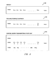
- an exemplary Detect supersequence 805 can be defined.
- the Detect supersequence 805 can include a repeating sequence of a single EIEOS (or other EOS) followed by a predefined number of instances of a particular training sequence (TS).
- TS training sequence
- the EIEOS can be transmitted, immediately followed by seven repeated instances of TS.
- the EIEOS can be sent again followed by seven additional instances of TS, and so on.
- This sequence can be repeated according to a particular predefined frequency.
- the EIEOS can reappear on the lanes approximately once every one thousand UIs ( ⁇ 1KUI) followed by the remainder of the Detect supersequence 805 .
- a receiver can monitor lanes for the presence of a repeating Detect supersequence 805 and upon validating the supersequence 705 can conclude that a remote agent is present, has been added (e.g., hot plugged) on the lanes, has awoke, or is reinitializing, etc.
- another supersequence 810 can be defined to indicate a polling, configuration, or loopback condition or state.
- lanes of a link can be monitored by a receiver for such a Poll/Config/Loop supersequence 810 to identify a polling state, configuration state, or loopback state or condition.
- a Poll/Config/Loop supersequence 810 can begin with an EIEOS followed by a predefined number of repeated instances of a TS. For instance, in one example the EIEOS can be followed by thirty-one (31) instances of TS with the EIEOS repeating approximately every four thousand UI (e.g., ⁇ 4KUI).
- a partial width transmitting state (PWTS) exit supersequence 815 can be defined.
- a PWTS exit supersequence can include an initial EIEOS to repeat to pre-condition lanes in advance of the sending of the first full sequence in the supersequence.
- the sequence to be repeated in supersequence 815 can begin with an EIEOS (to repeat approximately once every 1KUI).
- fast training sequences (FTS) can be utilized in lieu of other training sequences (TS), the FTS configured to assist in quicker bit lock, byte lock, and deskewing.
- an FTS can be unscrambled to further assist in bringing idle lanes back to active as quickly and non-disruptively as possible.
- the supersequence 815 can be interrupted and ended through the sending of a start of data sequence (SDS).
- SDS start of data sequence
- FTSp partial FTS
- FTSp can be sent to assist in synchronizing the new lanes to the active lanes, such as by allowing bits to be subtracted (or added) to the FTSp, among other examples.
- Supersequences such as Detect supersequence 705 and Poll/Config/Loop supersequence 710 , etc. can potentially be sent substantially throughout the initialization or re-initialization of a link.
- a receiver upon receiving and detecting a particular supersequence can, in some instances, respond by echoing the same supersequence to the transmitter over the lanes.
- the receiving and validation of a particular supersequence by transmitter and receiver can serve as a handshake to acknowledge a state or condition communicated through the supersequence. For instance, such a handshake (e.g., utilizing a Detect supersequence 705 ) can be used to identify reinitialization of a link.
- such a handshake can be utilized to indicate the end of an electrical reset or low power state, resulting in corresponding lanes being brought back up, among other examples.
- the end of the electrical reset can be identified, for instance, from a handshake between transmitter and receiver each transmitting a Detect supersequence 705 .
- lanes can be monitored for supersequences and use the supersequences in connection with the screening of lanes for detect, wake, state exits and entries, among other events.
- the predefined and predictable nature and form of supersequences can be further used to perform such initialization tasks as bit lock, byte lock, debouncing, descrambling, deskewing, adaptation, latency fixing, negotiated delays, and other potential uses.
- lanes can be substantially continuously monitored for such events to quicken the ability of the system to react to and process such conditions.
- transients can be introduced on lanes as a result of a variety of conditions. For instance, the addition or powering-on of a device can introduce transients onto the lane. Additionally, voltage irregularities can be presented on a lane because of poor lane quality or electrical failure. In some cases “bouncing” on a lane can produce false positives, such as a false EIEOS. However, in some implementations, while supersequences can be begin with an EIEOS, defined supersequences can further include additional sequences of data as well as a defined frequency at which the EIEOS will be repeated.
- a logic analyzer at the receiver can determine that the EIEOS is a false positive by validating data that succeeds the false EIEOS. For instance, if expected TS or other data does not follow the EIEOS or the EIEOS does not repeat within a particular one of the predefined frequencies of one of the predefined supersequences, the receiver logic analyzer can fail validation of the received EIEOS. As bouncing can occur at start up as a device is added to a line, false negatives can also result.
- a device upon being added to a set of lanes, can begin sending a Detect supersequence 705 to alert the other side of the link of its presence and begin initialization of the link.
- transients introduced on the lanes may corrupt the initial EIEOS, TS instances, and other data of the supersequence.
- a logic analyzer on the receiving device can continue to monitor the lanes and identify the next EIEOS sent by the new device in the repeating Detect supersequence 705 , among other examples.
- an HPI link is capable of operating at multiple speeds facilitated by the embedded clock.
- a slow mode can be defined.
- the slow mode can be used to assist in facilitating initialization of a link.
- Calibration of the link can involve software-based controllers providing logic for setting various calibrated characteristics of the link including which lanes the link is to use, the configuration of the lanes, the operational speed of the link, synchronization of the lanes and agents, deskew, target latency, among other potential characteristics.
- Such software-based tools can make use of external control points to add data to Physical layer registers to control various aspects of the Physical layer facilities and logic.
- Operational speed of a link can be considerably faster than the effective operation speed of software-based controllers utilized in initialization of the link.
- a slow mode can be used to allow use of such software-based controllers, such as during initialization or re-initialization of the link among other instances.
- Slow mode can be applied on lanes connecting a receiver and transmitter, for instance, when a link is turned on, initialized, reset, etc. to assist in facilitating calibration of the link.
- the clock can be embedded in the data so there are no separate clock lanes.
- the flits sent over the lanes can be scrambled to facilitate clock recovery.
- the receiver clock recovery unit can deliver sampling clocks to a receiver (i.e. the receiver recovers clock from the data and uses it to sample the incoming data).
- Receivers in some implementations continuously adapt to an incoming bit stream.
- By embedding the clock pinout can be potentially reduced.
- embedding the clock in the in-band data can alter the manner in which in-band reset is approached.
- a blocking link state (BLS) can be utilized after initialization.
- electrical ordered set supersequences may be utilized during initialization to facilitate the reset (e.g., as described above), among other considerations.
- the embedded clock can be common between the devices on a link and the common operational clock can be set during calibration and configuration of the link.
- HPI links can reference a common clock with drift buffers. Such implementation can realize lower latency than elastic buffers used in non-common reference clocks, among other potential advantages. Further, the reference clock distribution segments may be matched to within specified limits.
- an HPI link can be capable of operating at multiple speeds including a “slow mode” for default power-up, initialization, etc.
- the operational (or “fast”) speed or mode of each device can be statically set by BIOS.
- the common clock on the link can be configured based on the respective operational speeds of each device on either side of the link. For instance, the link speed can be based on the slower of the two device operations speeds, among other examples. Any operational speed change may be accompanied by a warm or cold reset.
- the link on power-on, the link initializes to Slow Mode with transfer rate of, for example, 100 MT/s. Software then sets up the two sides for operational speed of the link and begins the initialization.
- a sideband mechanism can be utilized to set up a link including the common clock on the link, for instance, in the absence or unavailability of a slow mode.
- a slow mode initialization phase in one embodiment, can use the same encoding, scrambling, training sequences (TS), states, etc. as operational speed but with potentially fewer features (e.g., no electrical parameter setup, no adaptation, etc.).
- Slow mode operation phase can also potentially use the same encoding, scrambling etc. (although other implementations may not) but may have fewer states and features compared to operational speed (e.g., no low power states).
- slow mode can be implemented using the native phase lock loop (PLL) clock frequency of the device.
- PLL phase lock loop
- HPI can support an emulated slow mode without changing PLL clock frequency. While some designs may use separate PLLs for slow and fast speed, in some implementations of HPI emulated slow mode can be achieved by allowing the PLL clock to runs at the same fast operational speed during slow mode. For instance, a transmitter can emulate a slower clock signal by repeating bits multiple times so as to emulate a slow high clock signal and then a slow low clock signal. The receiver can then oversample the received signal to locate edges emulated by the repeating bits and identify the bit. In such implementations, ports sharing a PLL may coexist at slow and fast speeds.
- a common slow mode speed can be initialized between two devices.
- the two devices on a link may have different fast operational speeds.
- a common slow mode speed can be configured, for instance, during a discovery phase or state on the link.
- an emulation multiple can be set as an integer (or non-integer) ratio of fast speed to slow speed, and the different fast speeds can be down-converted to work with the same slow speed.
- two device agents which support at least one common frequency may be hot attached irrespective of the speed at which the host port is running.
- Software discovery may then use the slow mode link to identify and setup the most optimal link operational speeds.
- the multiple is an integer ratio of fast speed to slow speed
- different fast speeds may work with the same slow speed, which may be used during the discovery phase (e.g., of hot attach).
- adaptation of lanes on a link can be supported.
- the Physical layer can support both receiver adaptation and transmitter, or sender, adaptation.
- receiver adaptation the transmitter on a lane can send sample data to the receiver which the receiver logic can process to identify shortcomings in the electrical characteristics of the lane and quality of the signal.
- the receiver can then make adjustments to the calibration of the lane to optimize the lane based on the analysis of the received sample data.
- transmitter adaptation the receiver can again receive sample data and develop metrics describing the quality of the lane but in this case communicate the metrics to the transmitter (e.g., using a backchannel, such as a software, hardware, embedded, sideband or other channel) to allow the transmitter to make adjustments to the lane based on the feedback.
- Receiver adaptation can be initiated at the start of the Polling state using the Polling supersequence sent from the remote transmitter.
- transmitter adaptation can be done by repeating the following for each transmitter parameters.
- Both agents can enter Loopback Pattern state as masters and transmit specified pattern.
- Both receivers can measure the metric (e.g. BER) for that particular transmitter setting at a remote agent.
- Both agents can go to Loopback Marker state and then Reset and use backchannels (slow mode TLS or sideband) to exchange metrics. Based on these metrics, the next transmitter setting can be identified. Eventually the optimal transmitter setting can be identified and saved for subsequent use.
- drift buffers can be utilized on each lane to transfer the respective receiver bit stream from the remote clock domain to the local clock domain.
- the latency of the drift buffers may be sufficient to handle sum of drift from all sources in electrical specification (e.g., voltage, temperature, the residual SSC introduced by reference clock routing mismatches, and so on) but as small as possible to reduce transport delay. If the drift buffer is too shallow, drift errors can result and manifest as series of CRC errors. Consequently, in some implementations, a drift alarm can be provided which can initiate a Physical layer reset before an actual drift error occurs, among other examples.
- HPI may support the two sides running at a same nominal reference clock frequency but with a ppm difference.
- frequency adjustment (or elasticity) buffers may be needed and can be readjusted during an extended BLS window or during special sequences which would occur periodically, among other examples.
- HPI PHY logical layer can be independent of the underlying transmission media provided the latency does not result in latency fixing errors or timeouts at the link layer, among other considerations.
- External interfaces can be provided in HPI to assist in management of the Physical layer.
- external signals from pins, fuses, other layers
- timers, control and status registers can be provided.
- the input signals may change at any time relative to PHY state but are to be observed by the Physical layer at specific points in a respective state.
- a changing alignment signal (as introduced below) may be received but have no effect after the link has entered a transmitting link state, among other examples.
- command register values can be observed by Physical layer entities only at specific points in time.
- Physical layer logic can take a snapshot of the value and use it in subsequent operations. Consequently, in some implementations, updates to command registers may be associated with a limited subset of specific periods (e.g., in a transmitting link state or when holding in Reset calibration, in slow mode transmitting link state) to avoid anomalous behavior.
- status values track hardware changes, the values read may depend on when they are read. Some status values, however, such as link map, latency, speed, etc., may not change after initialization. For instance, a re-initialization (or low power link state (LPLS), or L1 state, exit) is the only thing which may cause these to change (e.g., a hard lane failure in a TLS may not result in reconfiguration of link until re-initialization is triggered, among other examples).
- LPLS low power link state
- Interface signals can include signals that are external to but affect Physical layer behavior. Such interface signals can include, as examples, encoding and timing signals. Interface signals can be design specific. These signals can be an input or output. Some interface signals, such as termed semaphores and prefixed EO among other examples, can be active once per assertion edge, i.e., they may be deasserted and then reasserted to take effect again, among other examples. For instance, Table 1 includes an example listing of example functions:
- CSR timer default values can be provided in pairs—one for slow mode and one for operational speed. In some instances, the value 0 disables the timer (i.e., timeout never occurs).
- Timers can include those shown in Table 2, below.
- Primary timers can be used to time expected actions in a state. Secondary timers are used for aborting initializations which are not progressing or for making forward state transitions at precise times in an automated test equipment (or ATE) mode. In some cases, secondary timers can be much larger than the primary timers in a state. Exponential timer sets can be suffixed with exp and the timer value is 2 raised to the field value. For linear timers, the timer value is the field value. Either timer could use different granularities. Additionally, some timers in the power management section can be in a set called a timing profile. These can be associated with a timing diagram of the same name.
- Control registers can be late action and may be read or written by software in some instances. Late-action values can take effect (e.g., pass through from software-facing to hardware-facing stage) continuously in Reset.
- Control semaphores prefixed CP are RW1S and can be cleared by hardware. Control registers may be utilized to perform any of the items described herein. They may be modifiable and accessible by hardware, software, firmware, or a combination thereof.
- Status registers can be provided to track hardware changes (written and used by hardware) and can be read-only (but debug software may also be able to write to them). Such registers may not affect interoperability and can be typically complemented with many private status registers. Status semaphores (prefixed SP) can be mandated since they may be cleared by software to redo the actions which set the status. Default means initial (on reset) values can be provided as a subset of these status bits related to initialization. On an initialization abort, this register can be copied into a storage structure.
- Tool Box registers can be provided.
- testability tool-box registers in the Physical layer can provide pattern generation, pattern checking and loop back control mechanisms.
- Higher-level applications can make use of these registers along with electrical parameters to determine margins.
- Interconnect built in test may utilize this tool-box to determine margins.
- these registers can be used in conjunction with the specific registers described in previous sections, among other examples.
- HPI supports Reliability, Availability, and Serviceability (RAS) capabilities utilizing the Physical layer.
- HPI supports hot plug and remove with one or more layers, which may include software.
- Hot remove can include quiescing the link and an initialization begin state/signal can be cleared for the agent to be removed.
- a remote agent i.e. the one that is not being removed (e.g., the host agent)
- An in-band reset e.g., through BLS
- CRS Calibrate Reset State
- the agent to be removed can be removed (or can be held in targeted pin reset, powered down), among other examples and features. Indeed, some of the above events may be omitted and additional events can be added.
- Hot add can include initialization speed can default to slow and an initialization signal can be set on the agent to be added.
- Software can set speed to slow and may clear the initialization signal on the remote agent.
- the link can come up in slow mode and software can determine an operational speed. In some cases, no PLL relock of a remote is performed at this point.
- Operational speed can be set on both agents and an enable can be set for adaptation (if not done previously).
- the initialization begin indicator can be cleared on both agents and an in-band BLS reset can cause both agents to wait in CRS.
- Software can assert a warm reset (e.g., a targeted or self-reset) of an agent (to be added), which may cause a PLL to relock.
- Software may also set the initialization begin signal by any known logic and further set on remote (thus advancing it to Receiver Detect State (RDS)). Software can de-assert warm reset of the adding agent (thus advancing it to RDS). The link can then initialize at operational speed to a Transmitting Link State (TLS) (or to Loopback if the adaption signal is set), among other examples. Indeed, some of the above events may be omitted and additional events can be added.
- RDS Receiver Detect State
- a link in HPI in one embodiment, can be resilient against hard error on a single lane by configuring itself to less than full width (e.g. less than half the full width) which can thereby exclude the faulty lane.
- the configuration can be done by link state machine and unused lanes can be turned off in the configuration state. As a result, the flit may be sent across at a narrower width, among other examples.
- Lane reversal can be supported on some links.
- Lane reversal can refer, for instance, to lanes 0/1/2 . . . of a transmitter connected to lanes n/n ⁇ 1/n ⁇ 2 . . . of a receiver (e.g. n may equal 19 or 7, etc.).
- Lane reversal can be detected at the receiver as identified in a field of a TS header.
- the receiver can handle the lane reversal by starting in a Polling state by using physical lane n . . . 0 for logical lane 0 . . . n.
- references to a lane may refer to a logical lane number.
- polarity may be inverted (i.e. when a differential transmitter +/ ⁇ is connected to receiver ⁇ /+. Polarity can also be detected at a receiver from one or more TS header fields and handled, in one embodiment, in the Polling State.
- Processor 1000 includes any processor or processing device, such as a microprocessor, an embedded processor, a digital signal processor (DSP), a network processor, a handheld processor, an application processor, a co-processor, a system on a chip (SOC), or other device to execute code.
- processor 1000 in one embodiment, includes at least two cores—core 1001 and 1002 , which may include asymmetric cores or symmetric cores (the illustrated embodiment). However, processor 1000 may include any number of processing elements that may be symmetric or asymmetric.
- a processing element refers to hardware or logic to support a software thread.
- hardware processing elements include: a thread unit, a thread slot, a thread, a process unit, a context, a context unit, a logical processor, a hardware thread, a core, and/or any other element, which is capable of holding a state for a processor, such as an execution state or architectural state.
- a processing element in one embodiment, refers to any hardware capable of being independently associated with code, such as a software thread, operating system, application, or other code.
- a physical processor or processor socket typically refers to an integrated circuit, which potentially includes any number of other processing elements, such as cores or hardware threads.
- a core often refers to logic located on an integrated circuit capable of maintaining an independent architectural state, wherein each independently maintained architectural state is associated with at least some dedicated execution resources.
- a hardware thread typically refers to any logic located on an integrated circuit capable of maintaining an independent architectural state, wherein the independently maintained architectural states share access to execution resources.
- the line between the nomenclature of a hardware thread and core overlaps.
- a core and a hardware thread are viewed by an operating system as individual logical processors, where the operating system is able to individually schedule operations on each logical processor.
- Physical processor 1000 includes two cores-core 1001 and 1002 .
- core 1001 and 1002 are considered symmetric cores, i.e. cores with the same configurations, functional units, and/or logic.
- core 1001 includes an out-of-order processor core
- core 1002 includes an in-order processor core.
- cores 1001 and 1002 may be individually selected from any type of core, such as a native core, a software managed core, a core adapted to execute a native Instruction Set Architecture (ISA), a core adapted to execute a translated Instruction Set Architecture (ISA), a co-designed core, or other known core.
- ISA Native Instruction Set Architecture
- ISA translated Instruction Set Architecture
- co-designed core or other known core.
- some form of translation such as a binary translation
- some form of translation such as a binary translation
- the functional units illustrated in core 1001 are described in further detail below, as the units in core 1002 operate in a similar manner in the depicted embodiment.
- core 1001 includes two hardware threads 1001 a and 1001 b , which may also be referred to as hardware thread slots 1001 a and 1001 b . Therefore, software entities, such as an operating system, in one embodiment potentially view processor 1000 as four separate processors, i.e., four logical processors or processing elements capable of executing four software threads concurrently. As alluded to above, a first thread is associated with architecture state registers 1001 a , a second thread is associated with architecture state registers 1001 b , a third thread may be associated with architecture state registers 1002 a , and a fourth thread may be associated with architecture state registers 1002 b .
- each of the architecture state registers may be referred to as processing elements, thread slots, or thread units, as described above.
- architecture state registers 1001 a are replicated in architecture state registers 1001 b , so individual architecture states/contexts are capable of being stored for logical processor 1001 a and logical processor 1001 b .
- core 1001 other smaller resources, such as instruction pointers and renaming logic in allocator and renamer block 1030 may also be replicated for threads 1001 a and 1001 b .
- Some resources such as re-order buffers in reorder/retirement unit 1035 , ILTB 1020 , load/store buffers, and queues may be shared through partitioning.
- Other resources such as general purpose internal registers, page-table base register(s), low-level data-cache and data-TLB 1015 , execution unit(s) 1040 , and portions of out-of-order unit 1035 are potentially fully shared.
- Processor 1000 often includes other resources, which may be fully shared, shared through partitioning, or dedicated by/to processing elements.
- FIG. 10 an embodiment of a purely exemplary processor with illustrative logical units/resources of a processor is illustrated. Note that a processor may include, or omit, any of these functional units, as well as include any other known functional units, logic, or firmware not depicted.
- core 1001 includes a simplified, representative out-of-order (OOO) processor core. But an in-order processor may be utilized in different embodiments.
- the OOO core includes a branch target buffer 1020 to predict branches to be executed/taken and an instruction-translation buffer (I-TLB) 1020 to store address translation entries for instructions.
- I-TLB instruction-translation buffer
- Core 1001 further includes decode module 1025 coupled to fetch unit 1020 to decode fetched elements.
- Fetch logic in one embodiment, includes individual sequencers associated with thread slots 1001 a , 1001 b , respectively.
- core 1001 is associated with a first ISA, which defines/specifies instructions executable on processor 1000 .
- machine code instructions that are part of the first ISA include a portion of the instruction (referred to as an opcode), which references/specifies an instruction or operation to be performed.
- Decode logic 1025 includes circuitry that recognizes these instructions from their opcodes and passes the decoded instructions on in the pipeline for processing as defined by the first ISA.
- decoders 1025 include logic designed or adapted to recognize specific instructions, such as transactional instruction.
- the architecture or core 1001 takes specific, predefined actions to perform tasks associated with the appropriate instruction. It is important to note that any of the tasks, blocks, operations, and methods described herein may be performed in response to a single or multiple instructions; some of which may be new or old instructions.
- decoders 1026 in one embodiment, recognize the same ISA (or a subset thereof). Alternatively, in a heterogeneous core environment, decoders 1026 recognize a second ISA (either a subset of the first ISA or a distinct ISA).
- allocator and renamer block 1030 includes an allocator to reserve resources, such as register files to store instruction processing results.
- threads 1001 a and 1001 b are potentially capable of out-of-order execution, where allocator and renamer block 1030 also reserves other resources, such as reorder buffers to track instruction results.
- Unit 1030 may also include a register renamer to rename program/instruction reference registers to other registers internal to processor 1000 .
- Reorder/retirement unit 1035 includes components, such as the reorder buffers mentioned above, load buffers, and store buffers, to support out-of-order execution and later in-order retirement of instructions executed out-of-order.
- Scheduler and execution unit(s) block 1040 includes a scheduler unit to schedule instructions/operation on execution units. For example, a floating point instruction is scheduled on a port of an execution unit that has an available floating point execution unit. Register files associated with the execution units are also included to store information instruction processing results. Exemplary execution units include a floating point execution unit, an integer execution unit, a jump execution unit, a load execution unit, a store execution unit, and other known execution units.
- Lower level data cache and data translation buffer (D-TLB) 1050 are coupled to execution unit(s) 1040 .
- the data cache is to store recently used/operated on elements, such as data operands, which are potentially held in memory coherency states.
- the D-TLB is to store recent virtual/linear to physical address translations.
- a processor may include a page table structure to break physical memory into a plurality of virtual pages.
- cores 1001 and 1002 share access to higher-level or further-out cache, such as a second level cache associated with on-chip interface 1010 .
- higher-level or further-out refers to cache levels increasing or getting further way from the execution unit(s).
- higher—level cache is a last—level data cache-last cache in the memory hierarchy on processor 1000 —such as a second or third level data cache.
- higher level cache is not so limited, as it may be associated with or include an instruction cache.
- a trace cache a type of instruction cache—instead may be coupled after decoder 1025 to store recently decoded traces.
- an instruction potentially refers to a macro-instruction (i.e. a general instruction recognized by the decoders), which may decode into a number of micro-instructions (micro-operations).
- processor 1000 also includes on-chip interface module 1010 .
- on-chip interface 101 is to communicate with devices external to processor 1000 , such as system memory 1075 , a chipset (often including a memory controller hub to connect to memory 1075 and an I/O controller hub to connect peripheral devices), a memory controller hub, a northbridge, or other integrated circuit.
- bus 1005 may include any known interconnect, such as multi-drop bus, a point-to-point interconnect, a serial interconnect, a parallel bus, a coherent (e.g. cache coherent) bus, a layered protocol architecture, a differential bus, and a GTL bus.
- Memory 1075 may be dedicated to processor 1000 or shared with other devices in a system. Common examples of types of memory 1075 include DRAM, SRAM, non-volatile memory (NV memory), and other known storage devices. Note that device 1080 may include a graphic accelerator, processor or card coupled to a memory controller hub, data storage coupled to an I/O controller hub, a wireless transceiver, a flash device, an audio controller, a network controller, or other known device.
- NV memory non-volatile memory
- a memory controller hub is on the same package and/or die with processor 1000 .
- a portion of the core (an on-core portion) 1010 includes one or more controller(s) for interfacing with other devices such as memory 1075 or a graphics device 1080 .
- the configuration including an interconnect and controllers for interfacing with such devices is often referred to as an on-core (or un-core configuration).
- on-chip interface 1010 includes a ring interconnect for on-chip communication and a high-speed serial point-to-point link 1005 for off-chip communication.
- processor 1000 is capable of executing a compiler, optimization, and/or translator code 1077 to compile, translate, and/or optimize application code 1076 to support the apparatus and methods described herein or to interface therewith.
- a compiler often includes a program or set of programs to translate source text/code into target text/code.
- compilation of program/application code with a compiler is done in multiple phases and passes to transform hi-level programming language code into low-level machine or assembly language code.
- single pass compilers may still be utilized for simple compilation.
- a compiler may utilize any known compilation techniques and perform any known compiler operations, such as lexical analysis, preprocessing, parsing, semantic analysis, code generation, code transformation, and code optimization.
- a front-end i.e. generally where syntactic processing, semantic processing, and some transformation/optimization may take place
- a back-end i.e. generally where analysis, transformations, optimizations, and code generation takes place.
- Some compilers refer to a middle, which illustrates the blurring of delineation between a front-end and back end of a compiler.
- reference to insertion, association, generation, or other operation of a compiler may take place in any of the aforementioned phases or passes, as well as any other known phases or passes of a compiler.
- a compiler potentially inserts operations, calls, functions, etc.
- compiler code or dynamic optimization code may insert such operations/calls, as well as optimize the code for execution during runtime.
- binary code (already compiled code) may be dynamically optimized during runtime.
- the program code may include the dynamic optimization code, the binary code, or a combination thereof.
- a translator such as a binary translator, translates code either statically or dynamically to optimize and/or translate code. Therefore, reference to execution of code, application code, program code, or other software environment may refer to: (1) execution of a compiler program(s), optimization code optimizer, or translator either dynamically or statically, to compile program code, to maintain software structures, to perform other operations, to optimize code, or to translate code: (2) execution of main program code including operations/calls, such as application code that has been optimized/compiled; (3) execution of other program code, such as libraries, associated with the main program code to maintain software structures, to perform other software related operations, or to optimize code; or (4) a combination thereof.
- processor 1100 includes multiple domains. Specifically, a core domain 1130 includes a plurality of cores 1130 A- 1130 N, a graphics domain 1160 includes one or more graphics engines having a media engine 1165 , and a system agent domain 1110 .
- system agent domain 1110 handles power control events and power management, such that individual units of domains 1130 and 1160 (e.g. cores and/or graphics engines) are independently controllable to dynamically operate at an appropriate power mode/level (e.g. active, turbo, sleep, hibernate, deep sleep, or other Advanced Configuration Power Interface like state) in light of the activity (or inactivity) occurring in the given unit.
- an appropriate power mode/level e.g. active, turbo, sleep, hibernate, deep sleep, or other Advanced Configuration Power Interface like state
- Each of domains 1130 and 1160 may operate at different voltage and/or power, and furthermore the individual units within the domains each potentially operate at an independent frequency and voltage. Note that while only shown with three domains, understand the scope of the present invention is not limited in this regard and additional domains may be present in other embodiments.
- each core 1130 further includes low level caches in addition to various execution units and additional processing elements.
- the various cores are coupled to each other and to a shared cache memory that is formed of a plurality of units or slices of a last level cache (LLC) 1140 A- 1140 N; these LLCs often include storage and cache controller functionality and are shared amongst the cores, as well as potentially among the graphics engine too.
- LLC last level cache
- a ring interconnect 1150 couples the cores together, and provides interconnection between the core domain 1130 , graphics domain 1160 and system agent circuitry 1110 , via a plurality of ring stops 1152 A- 1152 N, each at a coupling between a core and LLC slice.
- interconnect 1150 is used to carry various information, including address information, data information, acknowledgement information, and snoop/invalid information.
- a ring interconnect is illustrated, any known on-die interconnect or fabric may be utilized. As an illustrative example, some of the fabrics discussed above (e.g. another on-die interconnect, On-chip System Fabric (OSF), an Advanced Microcontroller Bus Architecture (AMBA) interconnect, a multi-dimensional mesh fabric, or other known interconnect architecture) may be utilized in a similar fashion.
- OSF On-chip System Fabric
- AMBA Advanced Microcontroller Bus Architecture
- system agent domain 1110 includes display engine 1112 which is to provide control of and an interface to an associated display.
- System agent domain 1110 may include other units, such as: an integrated memory controller 1120 that provides for an interface to a system memory (e.g., a DRAM implemented with multiple DIMMs; coherence logic 1122 to perform memory coherence operations. Multiple interfaces may be present to enable interconnection between the processor and other circuitry. For example, in one embodiment at least one direct media interface (DMI) 1116 interface is provided as well as one or more PCIeTM interfaces 1114 . The display engine and these interfaces typically couple to memory via a PCIeTM bridge 1118 . Still further, to provide for communications between other agents, such as additional processors or other circuitry, one or more other interfaces may be provided.
- DMI direct media interface
- FIG. 12 shown is a block diagram of a representative core; specifically, logical blocks of a back-end of a core, such as core 1130 from FIG. 11 .
- the structure shown in FIG. 12 includes an out-of-order processor that has a front end unit 1270 used to fetch incoming instructions, perform various processing (e.g. caching, decoding, branch predicting, etc.) and passing instructions/operations along to an out-of-order (OOO) engine 1280 .
- OOO engine 1280 performs further processing on decoded instructions.
- out-of-order engine 1280 includes an allocate unit 1282 to receive decoded instructions, which may be in the form of one or more micro-instructions or uops, from front end unit 1270 , and allocate them to appropriate resources such as registers and so forth.
- the instructions are provided to a reservation station 1284 , which reserves resources and schedules them for execution on one of a plurality of execution units 1286 A- 1286 N.
- execution units may be present, including, for example, arithmetic logic units (ALUs), load and store units, vector processing units (VPUs), floating point execution units, among others.
- Results from these different execution units are provided to a reorder buffer (ROB) 1288 , which take unordered results and return them to correct program order.
- ROB reorder buffer
- both front end unit 1270 and out-of-order engine 1280 are coupled to different levels of a memory hierarchy. Specifically shown is an instruction level cache 1272 , that in turn couples to a mid-level cache 1276 , that in turn couples to a last level cache 1295 .
- last level cache 1295 is implemented in an on-chip (sometimes referred to as uncore) unit 1290 .
- unit 1290 is similar to system agent 810 of FIG. 8 .
- uncore 1290 communicates with system memory 1299 , which, in the illustrated embodiment, is implemented via ED RAM.
- execution units 1286 within out-of-order engine 1280 are in communication with a first level cache 1274 that also is in communication with mid-level cache 1276 .
- additional cores 1230 N- 2 - 1230 N can couple to LLC 1295 . Although shown at this high level in the embodiment of FIG. 12 , understand that various alterations and additional components may be present.
- System 1300 includes a component, such as a processor 1302 to employ execution units including logic to perform algorithms for process data, in accordance with the present invention, such as in the embodiment described herein.
- System 1300 is representative of processing systems based on the PENTIUM IIITM, PENTIUM 4TM, XeonTM, Itanium, XScaleTM and/or StrongARMTM microprocessors, although other systems (including PCs having other microprocessors, engineering workstations, set-top boxes and the like) may also be used.
- sample system 1300 executes a version of the WINDOWSTM operating system available from Microsoft Corporation of Redmond, Wash., although other operating systems (UNIX and Linux for example), embedded software, and/or graphical user interfaces, may also be used.
- WINDOWSTM operating system available from Microsoft Corporation of Redmond, Wash.
- other operating systems UNIX and Linux for example
- embedded software e.g., graphical user interfaces
- embodiments of the present invention are not limited to any specific combination of hardware circuitry and software.
- Embodiments are not limited to computer systems. Alternative embodiments of the present invention can be used in other devices such as handheld devices and embedded applications. Some examples of handheld devices include cellular phones, Internet Protocol devices, digital cameras, personal digital assistants (PDAs), and handheld PCs. Embedded applications can include a micro controller, a digital signal processor (DSP), system on a chip, network computers (NetPC), set-top boxes, network hubs, wide area network (WAN) switches, or any other system that can perform one or more instructions in accordance with at least one embodiment.
- DSP digital signal processor
- NetPC network computers
- Set-top boxes network hubs
- WAN wide area network
- processor 1302 includes one or more execution units 1308 to implement an algorithm that is to perform at least one instruction.
- One embodiment may be described in the context of a single processor desktop or server system, but alternative embodiments may be included in a multiprocessor system.
- System 1300 is an example of a ‘hub’ system architecture.
- the computer system 1300 includes a processor 1302 to process data signals.
- the processor 1302 includes a complex instruction set computer (CISC) microprocessor, a reduced instruction set computing (RISC) microprocessor, a very long instruction word (VLIW) microprocessor, a processor implementing a combination of instruction sets, or any other processor device, such as a digital signal processor, for example.
- CISC complex instruction set computer
- RISC reduced instruction set computing
- VLIW very long instruction word
- the processor 1302 is coupled to a processor bus 1310 that transmits data signals between the processor 1302 and other components in the system 1300 .
- the elements of system 1300 e.g. graphics accelerator 1312 , memory controller hub 1316 , memory 1320 , I/O controller hub 1324 , wireless transceiver 1326 , Flash BIOS 1328 , Network controller 1334 , Audio controller 1336 , Serial expansion port 1338 , I/O controller 1340 , etc.
- graphics accelerator 1312 e.g. graphics accelerator 1312 , memory controller hub 1316 , memory 1320 , I/O controller hub 1324 , wireless transceiver 1326 , Flash BIOS 1328 , Network controller 1334 , Audio controller 1336 , Serial expansion port 1338 , I/O controller 1340 , etc.
- the processor 1302 includes a Level 1 (L1) internal cache memory 1304 .
- the processor 1302 may have a single internal cache or multiple levels of internal caches. Other embodiments include a combination of both internal and external caches depending on the particular implementation and needs.
- Register file 1306 is to store different types of data in various registers including integer registers, floating point registers, vector registers, banked registers, shadow registers, checkpoint registers, status registers, and instruction pointer register.
- Execution unit 1308 including logic to perform integer and floating point operations, also resides in the processor 1302 .
- the processor 1302 includes a microcode (ucode) ROM to store microcode, which when executed, is to perform algorithms for certain macroinstructions or handle complex scenarios.
- microcode is potentially updateable to handle logic bugs/fixes for processor 1302 .
- execution unit 1308 includes logic to handle a packed instruction set 1309 . By including the packed instruction set 1309 in the instruction set of a general-purpose processor 1302 , along with associated circuitry to execute the instructions, the operations used by many multimedia applications may be performed using packed data in a general-purpose processor 1302 .
- System 1300 includes a memory 1320 .
- Memory 1320 includes a dynamic random access memory (DRAM) device, a static random access memory (SRAM) device, flash memory device, or other memory device.
- DRAM dynamic random access memory
- SRAM static random access memory
- Memory 1320 stores instructions and/or data represented by data signals that are to be executed by the processor 1302 .
- any of the aforementioned features or aspects of the invention may be utilized on one or more interconnect illustrated in FIG. 13 .
- an on-die interconnect which is not shown, for coupling internal units of processor 1302 implements one or more aspects of the invention described above.
- the invention is associated with a processor bus 1310 (e.g. other known high performance computing interconnect), a high bandwidth memory path 1318 to memory 1320 , a point-to-point link to graphics accelerator 1312 (e.g. a Peripheral Component Interconnect express (PCIe) compliant fabric), a controller hub interconnect 1322 , an I/O or other interconnect (e.g. USB, PCI, PCIe) for coupling the other illustrated components.
- PCIe Peripheral Component Interconnect express
- Some examples of such components include the audio controller 1336 , firmware hub (flash BIOS) 1328 , wireless transceiver 1326 , data storage 1324 , legacy I/O controller 1310 containing user input and keyboard interfaces 1342 , a serial expansion port 1338 such as Universal Serial Bus (USB), and a network controller 1334 .
- the data storage device 1324 can comprise a hard disk drive, a floppy disk drive, a CD-ROM device, a flash memory device, or other mass storage device.
- multiprocessor system 1400 is a point-to-point interconnect system, and includes a first processor 1470 and a second processor 1480 coupled via a point-to-point interconnect 1450 .
- processors 1470 and 1480 may be some version of a processor.
- 1452 and 1454 are part of a serial, point-to-point coherent interconnect fabric, such as a high-performance architecture. As a result, the invention may be implemented within the QPI architecture.
- processors 1470 , 1480 While shown with only two processors 1470 , 1480 , it is to be understood that the scope of the present invention is not so limited. In other embodiments, one or more additional processors may be present in a given processor.
- Processors 1470 and 1480 are shown including integrated memory controller units 1472 and 1482 , respectively.
- Processor 1470 also includes as part of its bus controller units point-to-point (P-P) interfaces 1476 and 1478 ; similarly, second processor 1480 includes P-P interfaces 1486 and 1488 .
- Processors 1470 , 1480 may exchange information via a point-to-point (P-P) interface 1450 using P-P interface circuits 1478 , 1488 .
- IMCs 1472 and 1482 couple the processors to respective memories, namely a memory 1432 and a memory 1434 , which may be portions of main memory locally attached to the respective processors.
- Processors 1470 , 1480 each exchange information with a chipset 1490 via individual P-P interfaces 1452 , 1454 using point to point interface circuits 1476 , 1494 , 1486 , 1498 .
- Chipset 1490 also exchanges information with a high-performance graphics circuit 1438 via an interface circuit 1492 along a high-performance graphics interconnect 1439 .
- a shared cache (not shown) may be included in either processor or outside of both processors: yet connected with the processors via P-P interconnect, such that either or both processors' local cache information may be stored in the shared cache if a processor is placed into a low power mode.
- first bus 1416 may be a Peripheral Component Interconnect (PCI) bus, or a bus such as a PCI Express bus or another third generation I/O interconnect bus, although the scope of the present invention is not so limited.
- PCI Peripheral Component Interconnect
- various I/O devices 1414 are coupled to first bus 1416 , along with a bus bridge 1418 which couples first bus 1416 to a second bus 1420 .
- second bus 1420 includes a low pin count (LPC) bus.
- LPC low pin count
- Various devices are coupled to second bus 1420 including, for example, a keyboard and/or mouse 1422 , communication devices 1427 and a storage unit 1428 such as a disk drive or other mass storage device which often includes instructions/code and data 1430 , in one embodiment.
- an audio I/O 1424 is shown coupled to second bus 1420 .
- Note that other architectures are possible, where the included components and interconnect architectures vary. For example, instead of the point-to-point architecture of FIG. 14 , a system may implement a multi-drop bus or other such architecture.
- SOC 1500 is included in user equipment (UE).
- UE refers to any device to be used by an end-user to communicate, such as a hand-held phone, smartphone, tablet, ultra-thin notebook, notebook with broadband adapter, or any other similar communication device.
- a UE connects to a base station or node, which potentially corresponds in nature to a mobile station (MS) in a GSM network.
- MS mobile station
- SOC 1500 includes 2 cores— 1506 and 1507 . Similar to the discussion above, cores 1506 and 1507 may conform to an Instruction Set Architecture, such as an Intel® Architecture CoreTM-based processor, an Advanced Micro Devices, Inc. (AMD) processor, a MIPS-based processor, an ARM-based processor design, or a customer thereof, as well as their licensees or adopters. Cores 1506 and 1507 are coupled to cache control 1508 that is associated with bus interface unit 1509 and L2 cache 1511 to communicate with other parts of system 1500 . Interconnect 1510 includes an on-chip interconnect, such as an IOSF, AMBA, or other interconnect discussed above, which potentially implements one or more aspects of described herein.
- an Intel® Architecture CoreTM-based processor such as an Intel® Architecture CoreTM-based processor, an Advanced Micro Devices, Inc. (AMD) processor, a MIPS-based processor, an ARM-based processor design, or a customer thereof, as well as their licensees or adopters.
- Interconnect 1510 provides communication channels to the other components, such as a Subscriber Identity Module (SIM) 1530 to interface with a SIM card, a boot rom 1535 to hold boot code for execution by cores 1506 and 1507 to initialize and boot SOC 1500 , a SDRAM controller 1540 to interface with external memory (e.g. DRAM 1560 ), a flash controller 1545 to interface with non-volatile memory (e.g. Flash 1565 ), a peripheral control 1550 (e.g. Serial Peripheral Interface) to interface with peripherals, video codecs 1520 and Video interface 1525 to display and receive input (e.g. touch enabled input), GPU 1515 to perform graphics related computations, etc. Any of these interfaces may incorporate aspects of the invention described herein.
- SIM Subscriber Identity Module
- boot rom 1535 to hold boot code for execution by cores 1506 and 1507 to initialize and boot SOC 1500
- SDRAM controller 1540 to interface with external memory (e.g. DRAM 1560 )
- flash controller 1545
- the system illustrates peripherals for communication, such as a Bluetooth module 1570 , 3G modem 1575 , GPS 1585 , and WiFi 1585 .
- a UE includes a radio for communication.
- these peripheral communication modules are not all required.
- a radio for external communication is to be included.
- a design may go through various stages, from creation to simulation to fabrication.
- Data representing a design may represent the design in a number of manners.
- the hardware may be represented using a hardware description language or another functional description language.
- a circuit level model with logic and/or transistor gates may be produced at some stages of the design process.
- most designs, at some stage reach a level of data representing the physical placement of various devices in the hardware model.
- the data representing the hardware model may be the data specifying the presence or absence of various features on different mask layers for masks used to produce the integrated circuit.
- the data may be stored in any form of a machine readable medium.
- a memory or a magnetic or optical storage such as a disc may be the machine readable medium to store information transmitted via optical or electrical wave modulated or otherwise generated to transmit such information.
- an electrical carrier wave indicating or carrying the code or design is transmitted, to the extent that copying, buffering, or re-transmission of the electrical signal is performed, a new copy is made.
- a communication provider or a network provider may store on a tangible, machine-readable medium, at least temporarily, an article, such as information encoded into a carrier wave, embodying techniques of embodiments of the present invention.
- a module as used herein refers to any combination of hardware, software, and/or firmware.
- a module includes hardware, such as a micro-controller, associated with a non-transitory medium to store code adapted to be executed by the micro-controller. Therefore, reference to a module, in one embodiment, refers to the hardware, which is specifically configured to recognize and/or execute the code to be held on a non-transitory medium.
- use of a module refers to the non-transitory medium including the code, which is specifically adapted to be executed by the microcontroller to perform predetermined operations.
- the term module in this example may refer to the combination of the microcontroller and the non-transitory medium.
- a first and a second module may share hardware, software, firmware, or a combination thereof, while potentially retaining some independent hardware, software, or firmware.
- use of the term logic includes hardware, such as transistors, registers, or other hardware, such as programmable logic devices.
- phrase ‘configured to,’ refers to arranging, putting together, manufacturing, offering to sell, importing and/or designing an apparatus, hardware, logic, or element to perform a designated or determined task.
- an apparatus or element thereof that is not operating is still ‘configured to’ perform a designated task if it is designed, coupled, and/or interconnected to perform said designated task.
- a logic gate may provide a 0 or a 1 during operation.
- a logic gate ‘configured to’ provide an enable signal to a clock does not include every potential logic gate that may provide a 1 or 0. Instead, the logic gate is one coupled in some manner that during operation the 1 or 0 output is to enable the clock.
- use of the phrases ‘to,’ ‘capable of/to,’ and or ‘operable to,’ in one embodiment refers to some apparatus, logic, hardware, and/or element designed in such a way to enable use of the apparatus, logic, hardware, and/or element in a specified manner.
- use of to, capable to, or operable to, in one embodiment refers to the latent state of an apparatus, logic, hardware, and/or element, where the apparatus, logic, hardware, and/or element is not operating but is designed in such a manner to enable use of an apparatus in a specified manner.
- a value includes any known representation of a number, a state, a logical state, or a binary logical state. Often, the use of logic levels, logic values, or logical values is also referred to as 1's and 0's, which simply represents binary logic states. For example, a 1 refers to a high logic level and 0 refers to a low logic level.
- a storage cell such as a transistor or flash cell, may be capable of holding a single logical value or multiple logical values.
- the decimal number ten may also be represented as a binary value of 1010 and a hexadecimal letter A. Therefore, a value includes any representation of information capable of being held in a computer system.
- states may be represented by values or portions of values.
- a first value such as a logical one
- a second value such as a logical zero
- reset and set in one embodiment, refer to a default and an updated value or state, respectively.
- a default value potentially includes a high logical value, i.e. reset
- an updated value potentially includes a low logical value, i.e. set.
- any combination of values may be utilized to represent any number of states.
- a non-transitory machine-accessible/readable medium includes any mechanism that provides (i.e., stores and/or transmits) information in a form readable by a machine, such as a computer or electronic system.
- a non-transitory machine-accessible medium includes random-access memory (RAM), such as static RAM (SRAM) or dynamic RAM (DRAM); ROM; magnetic or optical storage medium; flash memory devices; electrical storage devices; optical storage devices; acoustical storage devices; other form of storage devices for holding information received from transitory (propagated) signals (e.g., carrier waves, infrared signals, digital signals); etc, which are to be distinguished from the non-transitory mediums that may receive information there from.
- RAM random-access memory
- SRAM static RAM
- DRAM dynamic RAM
- ROM magnetic or optical storage medium
- flash memory devices electrical storage devices
- optical storage devices e.g., optical storage devices
- acoustical storage devices other form of storage devices for holding information received from transitory (propagated) signals (e.g., carrier waves, infrared signals, digital signals); etc, which are to be distinguished from the non-transitory mediums that may receive information there from.
- a machine-readable medium may include any mechanism for storing or transmitting information in a form readable by a machine (e.g., a computer), but is not limited to, floppy diskettes, optical disks, Compact Disc, Read-Only Memory (CD-ROMs), and magneto-optical disks, Read-Only Memory (ROMs), Random Access Memory (RAM), Erasable Programmable Read-Only Memory (EPROM), Electrically Erasable Programmable Read-Only Memory (EEPROM), magnetic or optical cards, flash memory, or a tangible, machine-readable storage used in the transmission of information over the Internet via electrical, optical, acoustical or other forms of propagated signals (e.g., carrier waves, infrared signals, digital signals, etc.). Accordingly, the computer-
- One or more embodiments may provide an apparatus, a system, a machine readable storage, a machine readable medium, and a method to initialize a link, wherein the link is to include a number of lanes, a transmitter and a receiver are to be coupled to each lane in the number of lanes, and re-initialization of the link is to include transmission of a predefined sequence on each of the lanes, wherein re-initialization is to be provided without termination of the link.
- the predefined sequence is to be sent from the transmitter to the receiver and the receiver is to repeat the predefined sequence to the transmitter.
- the sequence includes an electric idle exit ordered set (EIEOS).
- EIEOS electric idle exit ordered set
- the sequence further includes a plurality of instances of a training sequence.
- the EIEOS is to be repeated is the sequence according to a minimum frequency.
- the sequence is to be repeated until the link is initialized.
- One or more examples can further provide validating a received instances of the predefined sequence to detect an agent on the link.
- the link comprises a differential serial data link.
- the sequence is to be sent during a reset state to signal exit from the reset state.
- One or more embodiments may provide an apparatus, a system, a machine readable storage, a machine readable medium, and a method to transmit, over lanes of a differential serial data link, a predefined sequence to another entity connected to the data link, receive an acknowledgement of predefined sequence from the other entity, and use the predefined sequence to facilitate initialization of the data link.
- the flit can be sent from a first device to a second device over the data link.
- the first second devices can include microprocessors, graphics accelerators, and other devices.
- One or more embodiments may provide an apparatus, a system, a machine readable storage, a machine readable medium, and a method to to detect, on a link including a number of lanes, a predefined sequence on each of the lanes and determine a state of another agent based on the detection of the predefined sequence.
- One or more examples can further provide echoing the predefined sequence to the other agent.
- the sequence includes an EIEOS and detection of the predefined sequence includes validation of the sequence.
- validation of the sequence is based at least in part on identifying that the EIEOS is repeated according to a predefined frequency.
- the sequence is repeated throughout a particular link initializations state.
- the sequence indicates an initialization state.
- the initialization state is included in a reinitialization of the link.
- the sequence is detected during a reset state and indicates an exit from the reset state.
- One or more embodiments may provide an apparatus, a system, a machine readable storage, a machine readable medium, and a method to monitor looping during initialization of a link and cause initialization of the link to suspend in response to determining unsuccessful looping during the initialization.
- One or more examples can further provide maintaining a count of loops in a state machine during the initialization.
- the count is to be maintained on each agent communicatively connected using the link.
- the count is to be reset upon a successful initialization of the link.
- successful initialization of the link comprises entering a link transmitting state.
- a loop includes re-entering a reset state of a link training state machine.
- the initialization of the link is to be suspended in a reset state of a link training state machine.
- a suspended initialization of the link is to restart in response to a command from a controller.
- the link has a link width of 20 lanes.
- One or more embodiments may provide an apparatus, a system, a machine readable storage, a machine readable medium, and a method to determine whether to perform one or more initialization tasks in connection with a particular initialization state; and apply a short timer to transition from the particular state based on determining whether to perform the initialization tasks.
- One or more examples can further provide applying a second short timer to transition from a second initialization state and the second short timer is of a duration different from the first short time.
- the short timer is to be applied based on a determination not to perform the initialization tasks.
- a long timer for the particular initialization state is to be applied based on a determination to perform the initialization tasks.
- the determination is based on an indication that the short timer is enabled.
- the short timer is enabled by a software-based controller.
- the short timer is to be enabled based on a determination that configuration associated with the initialization task is completed.
- the link comprises a differential serial data link.
- One or more embodiments may provide an apparatus, a system, a machine readable storage, a machine readable medium, and a method to transmit flits at a first speed in a first mode, and to transmit flits at a second speed in a second mode, and wherein a phased locked loop (PLL) speed is the same in the first mode and the second mode.
- PLL phased locked loop
- the first speed comprises an operational speed and the second speed comprises a slow speed.
- the slow speed is to be emulated by the operational speed.
- emulating the slow speed comprises sending a series of bits at the operational speed to simulate a bit in the slow mode.
- the physical layer logic is further to transition from the first speed to the second speed.
- the transition is based on a request of an at least partially software-based controller.
- One or more embodiments may provide an apparatus, a system, a machine readable storage, a machine readable medium, and a method to determine an operational speed of a first device to be connected on a link to a second device: determine an operational speed of the second device; and determine a common slow speed to be applied by the first and second devices during transmission of data on the link.
- the common slow speed is determined during an initialization of the link.
- the operational speed of the first device is different from the operational speed of the second device and the initialization of the link further includes determining a common operational speed.
- the common operation speed is based on the slower of the operational speeds of the first and second devices.
- determining the common slow mode includes determining a first ratio to be applied to the operational speed of the first device to realize the common slow speed and determining a second ration to be applied to the operational speed of the second device to realize the common slow speed.
- the common slow speed is to be emulated by the operational speeds.
- emulating the slow speed comprises sending a series of bits at a respective operational speed to simulate a bit in the common slow mode.
- One or more examples can further provide a physical layer (PHY) configured to be coupled to a link, the link including a first number of lanes, wherein the PHY includes a synchronization (sync) counter, and wherein the PHY is to transmit an Electrically Idle Exit Order Set (EIEOS) aligned with the sync counter associated with a training sequence.
- PHY physical layer
- Sync synchronization
- EIEOS Electrically Idle Exit Order Set
- a sync counter value from the sync counter is not exchanged during each training sequence.
- the EIEOS alignment with the sync counter is to act as a proxy for exchanging the sync counter value from the sync counter during each training sequence.
- One or more examples can further provide physical layer (PHY) configured to be coupled to a link, the PHY to include a software modifiable register including a control field, and a PHY state machine to transition between a plurality of states, wherein the PHY state machine is to hold transition between a first state and a second state based on a first value of the control field of the register.
- PHY physical layer
- the PHY state machine is to transition between the first state and the second state in response to software updating the control field of the register to a second value.
- One or more examples can further provide a physical layer (PHY) configured to be coupled to a link, the PHY to include a PHY state machine to transition between a plurality of states, wherein the PHY state machine is capable of transitioning from a first state to a second state based on a handshake event and transitioning the PHY from a third state to a fourth state based on a primary timer event.
- PHY physical layer
- the PHY state machine is capable of transitioning the PHY from a fifth state to a sixth state based on a primary time event in combination with a secondary timer event
- One or more examples can further provide a physical layer (PHY) configured to be coupled to a link, the link including a first number of lanes, wherein the PHY is to transmit flits at a first speed, and to transmit flits at a second speed, and wherein a phased locked loop (PLL) speed is the same in the fast mode and the slow mode.
- PHY physical layer
- PLL phased locked loop
- the first speed is a slow speed and the second speed is a fast speed
- One or more examples can further provide a physical layer (PHY) configured to be coupled to a link, the link including a first number of lanes, wherein the PHY is to transmit flits at a slow speed in a slow mode, and to transmit flits at a fast speed in a fast mode, the fast speed being more than 2 ⁇ the slow speed, and wherein a phased locked loop (PLL) speed is the same in the fast mode and the slow mode.
- PHY physical layer
- PHY phased locked loop
Abstract
Re-initialization of a link can take place without termination of the link, where the link includes, a transmitter and a receiver are to be coupled to each lane in the number of lanes, and re-initialization of the link is to include transmission of a pre-defined sequence on each of the lanes.
Description
This application is a continuation of U.S. application Ser. No. 13/976,960, filed on Jul. 27, 2016, now U.S. Pat. No. 9,418,035, and entitled HIGH PERFORMANCE INTERCONNECT PHYSICAL LAYER which is a national stage application under 35 U.S.C. § 371 of PCT International Application Serial No. PCT/US2013/032690, filed on Mar. 25, 2013 and entitled HIGH PERFORMANCE INTERCONNECT PHYSICAL LAYER, which application claims the benefit of priority to U.S. Provisional Patent Application Ser. No. 61/717,091 filed on Oct. 22, 2012 and entitled METHOD, APPARATUS, SYSTEM FOR A HIGH PERFORMANCE INTERCONNECT ARCHITECTURE. The disclosures of the prior applications are considered part of and are hereby incorporated by reference in their entirety in the disclosure of this application.
The present disclosure relates in general to the field of computer development, and more specifically, to software development involving coordination of mutually-dependent constrained systems.
Advances in semi-conductor processing and logic design have permitted an increase in the amount of logic that may be present on integrated circuit devices. As a corollary, computer system configurations have evolved from a single or multiple integrated circuits in a system to multiple cores, multiple hardware threads, and multiple logical processors present on individual integrated circuits, as well as other interfaces integrated within such processors. A processor or integrated circuit typically comprises a single physical processor die, where the processor die may include any number of cores, hardware threads, logical processors, interfaces, memory, controller hubs, etc.
As a result of the greater ability to fit more processing power in smaller packages, smaller computing devices have increased in popularity. Smartphones, tablets, ultrathin notebooks, and other user equipment have grown exponentially. However, these smaller devices are reliant on servers both for data storage and complex processing that exceeds the form factor. Consequently, the demand in the high-performance computing market (i.e. server space) has also increased. For instance, in modern servers, there is typically not only a single processor with multiple cores, but also multiple physical processors (also referred to as multiple sockets) to increase the computing power. But as the processing power grows along with the number of devices in a computing system, the communication between sockets and other devices becomes more critical.
In fact, interconnects have grown from more traditional multi-drop buses that primarily handled electrical communications to full blown interconnect architectures that facilitate fast communication. Unfortunately, as the demand for future processors to consume at even higher-rates corresponding demand is placed on the capabilities of existing interconnect architectures.
Like reference numbers and designations in the various drawings indicate like elements.
In the following description, numerous specific details are set forth, such as examples of specific types of processors and system configurations, specific hardware structures, specific architectural and micro architectural details, specific register configurations, specific instruction types, specific system components, specific processor pipeline stages, specific interconnect layers, specific packet/transaction configurations, specific transaction names, specific protocol exchanges, specific link widths, specific implementations, and operation etc. in order to provide a thorough understanding of the present invention. It may be apparent, however, to one skilled in the art that these specific details need not necessarily be employed to practice the subject matter of the present disclosure. In other instances, well detailed description of known components or methods has been avoided, such as specific and alternative processor architectures, specific logic circuits/code for described algorithms, specific firmware code, low-level interconnect operation, specific logic configurations, specific manufacturing techniques and materials, specific compiler implementations, specific expression of algorithms in code, specific power down and gating techniques/logic and other specific operational details of computer system in order to avoid unnecessarily obscuring the present disclosure.
Although the following embodiments may be described with reference to energy conservation, energy efficiency, processing efficiency, and so on in specific integrated circuits, such as in computing platforms or microprocessors, other embodiments are applicable to other types of integrated circuits and logic devices. Similar techniques and teachings of embodiments described herein may be applied to other types of circuits or semiconductor devices that may also benefit from such features. For example, the disclosed embodiments are not limited to server computer system, desktop computer systems, laptops, Ultrabooks™, but may be also used in other devices, such as handheld devices, smartphones, tablets, other thin notebooks, systems on a chip (SOC) devices, and embedded applications. Some examples of handheld devices include cellular phones, Internet protocol devices, digital cameras, personal digital assistants (PDAs), and handheld PCs. Here, similar techniques for a high-performance interconnect may be applied to increase performance (or even save power) in a low power interconnect. Embedded applications typically include a microcontroller, a digital signal processor (DSP), a system on a chip, network computers (NetPC), set-top boxes, network hubs, wide area network (WAN) switches, or any other system that can perform the functions and operations taught below. Moreover, the apparatus', methods, and systems described herein are not limited to physical computing devices, but may also relate to software optimizations for energy conservation and efficiency. As may become readily apparent in the description below, the embodiments of methods, apparatus', and systems described herein (whether in reference to hardware, firmware, software, or a combination thereof) may be considered vital to a “green technology” future balanced with performance considerations.
As computing systems are advancing, the components therein are becoming more complex. The interconnect architecture to couple and communicate between the components has also increased in complexity to ensure bandwidth demand is met for optimal component operation. Furthermore, different market segments demand different aspects of interconnect architectures to suit the respective market. For example, servers require higher performance, while the mobile ecosystem is sometimes able to sacrifice overall performance for power savings. Yet, it is a singular purpose of most fabrics to provide highest possible performance with maximum power saving. Further, a variety of different interconnects can potentially benefit from subject matter described herein.
The Peripheral Component Interconnect (PCI) Express (PCIe) interconnect fabric architecture and QuickPath Interconnect (QPI) fabric architecture, among other examples, can potentially be improved according to one or more principles described herein, among other examples. For instance, a primary goal of PCIe is to enable components and devices from different vendors to inter-operate in an open architecture, spanning multiple market segments; Clients (Desktops and Mobile), Servers (Standard and Enterprise), and Embedded and Communication devices. PCI Express is a high performance, general purpose I/O interconnect defined for a wide variety of future computing and communication platforms. Some PCI attributes, such as its usage model, load-store architecture, and software interfaces, have been maintained through its revisions, whereas previous parallel bus implementations have been replaced by a highly scalable, fully serial interface. The more recent versions of PCI Express take advantage of advances in point-to-point interconnects, Switch-based technology, and packetized protocol to deliver new levels of performance and features. Power Management, Quality Of Service (QoS), Hot-Plug/Hot-Swap support, Data Integrity, and Error Handling are among some of the advanced features supported by PCI Express. Although the primary discussion herein is in reference to a new high-performance interconnect (HPI) architecture, aspects of the invention described herein may be applied to other interconnect architectures, such as a PCIe-compliant architecture, a QPI-compliant architecture, a MIPI compliant architecture, a high-performance architecture, or other known interconnect architecture.
Referring to FIG. 1 , an embodiment of a fabric composed of point-to-point Links that interconnect a set of components is illustrated. System 100 includes processor 105 and system memory 110 coupled to controller hub 115. Processor 105 can include any processing element, such as a microprocessor, a host processor, an embedded processor, a co-processor, or other processor. Processor 105 is coupled to controller hub 115 through front-side bus (FSB) 106. In one embodiment, FSB 106 is a serial point-to-point interconnect as described below. In another embodiment, link 106 includes a serial, differential interconnect architecture that is compliant with different interconnect standard.
In one embodiment, controller hub 115 can include a root hub, root complex, or root controller, such as in a PCIc interconnection hierarchy. Examples of controller hub 115 include a chipset, a memory controller hub (MCH), a northbridge, an interconnect controller hub (ICH) a southbridge, and a root controller/hub. Often the term chipset refers to two physically separate controller hubs, e.g., a memory controller hub (MCH) coupled to an interconnect controller hub (ICH). Note that current systems often include the MCH integrated with processor 105, while controller 115 is to communicate with I/O devices, in a similar manner as described below. In some embodiments, peer-to-peer routing is optionally supported through root complex 115.
Here, controller hub 115 is coupled to switch/bridge 120 through serial link 119. Input/ output modules 117 and 121, which may also be referred to as interfaces/ ports 117 and 121, can include/implement a layered protocol stack to provide communication between controller hub 115 and switch 120. In one embodiment, multiple devices are capable of being coupled to switch 120.
Switch/bridge 120 routes packets/messages from device 125 upstream, i.e. up a hierarchy towards a root complex, to controller hub 115 and downstream, i.e. down a hierarchy away from a root controller, from processor 105 or system memory 110 to device 125. Switch 120, in one embodiment, is referred to as a logical assembly of multiple virtual PCI-to-PCI bridge devices. Device 125 includes any internal or external device or component to be coupled to an electronic system, such as an I/O device, a Network Interface Controller (NIC), an add-in card, an audio processor, a network processor, a hard-drive, a storage device, a CD/DVD ROM, a monitor, a printer, a mouse, a keyboard, a router, a portable storage device, a Firewire device, a Universal Serial Bus (USB) device, a scanner, and other input/output devices. Often in the PCIe vernacular, such as device, is referred to as an endpoint. Although not specifically shown, device 125 may include a bridge (e.g., a PCIe to PCI/PCI-X bridge) to support legacy or other versions of devices or interconnect fabrics supported by such devices.
Turning to FIG. 2 an embodiment of a layered protocol stack is illustrated. Layered protocol stack 200 can includes any form of a layered communication stack, such as a QPI stack, a PCIc stack, a next generation high performance computing interconnect (HPI) stack, or other layered stack. In one embodiment, protocol stack 200 can include transaction layer 205, link layer 210, and physical layer 220. An interface, such as interfaces 117, 118, 121, 122, 126, and 131 in FIG. 1 , may be represented as communication protocol stack 200. Representation as a communication protocol stack may also be referred to as a module or interface implementing/including a protocol stack.
Packets can be used to communicate information between components. Packets can be formed in the Transaction Layer 205 and Data Link Layer 210 to carry the information from the transmitting component to the receiving component. As the transmitted packets flow through the other layers, they are extended with additional information used to handle packets at those layers. At the receiving side the reverse process occurs and packets get transformed from their Physical Layer 220 representation to the Data Link Layer 210 representation and finally (for Transaction Layer Packets) to the form that can be processed by the Transaction Layer 205 of the receiving device.
In one embodiment, transaction layer 205 can provide an interface between a device's processing core and the interconnect architecture, such as Data Link Layer 210 and Physical Layer 220. In this regard, a primary responsibility of the transaction layer 205 can include the assembly and disassembly of packets (i.e., transaction layer packets, or TLPs). The translation layer 205 can also manage credit-based flow control for TLPs. In some implementations, split transactions can be utilized, i.e., transactions with request and response separated by time, allowing a link to carry other traffic while the target device gathers data for the response, among other examples.
Credit-based flow control can be used to realize virtual channels and networks utilizing the interconnect fabric. In one example, a device can advertise an initial amount of credits for each of the receive buffers in Transaction Layer 205. An external device at the opposite end of the link, such as controller hub 115 in FIG. 1 , can count the number of credits consumed by each TLP. A transaction may be transmitted if the transaction does not exceed a credit limit. Upon receiving a response an amount of credit is restored. One example of an advantage of such a credit scheme is that the latency of credit return does not affect performance, provided that the credit limit is not encountered, among other potential advantages.
In one embodiment, four transaction address spaces can include a configuration address space, a memory address space, an input/output address space, and a message address space. Memory space transactions include one or more of read requests and write requests to transfer data to/from a memory-mapped location. In one embodiment, memory space transactions are capable of using two different address formats, e.g., a short address format, such as a 32-bit address, or a long address format, such as 64-bit address. Configuration space transactions can be used to access configuration space of various devices connected to the interconnect. Transactions to the configuration space can include read requests and write requests. Message space transactions (or, simply messages) can also be defined to support in-band communication between interconnect agents. Therefore, in one example embodiment, transaction layer 205 can assemble packet header/payload 206.
Quickly referring to FIG. 3 , an example embodiment of a transaction layer packet descriptor is illustrated. In one embodiment, transaction descriptor 300 can be a mechanism for carrying transaction information. In this regard, transaction descriptor 300 supports identification of transactions in a system. Other potential uses include tracking modifications of default transaction ordering and association of transaction with channels. For instance, transaction descriptor 300 can include global identifier field 302, attributes field 304 and channel identifier field 306. In the illustrated example, global identifier field 302 is depicted comprising local transaction identifier field 308 and source identifier field 310. In one embodiment, global transaction identifier 302 is unique for all outstanding requests.
According to one implementation, local transaction identifier field 308 is a field generated by a requesting agent, and can be unique for all outstanding requests that require a completion for that requesting agent. Furthermore, in this example, source identifier 310 uniquely identifies the requestor agent within an interconnect hierarchy. Accordingly, together with source ID 310, local transaction identifier 308 field provides global identification of a transaction within a hierarchy domain.
Attributes field 304 specifies characteristics and relationships of the transaction. In this regard, attributes field 304 is potentially used to provide additional information that allows modification of the default handling of transactions. In one embodiment, attributes field 304 includes priority field 312, reserved field 314, ordering field 316, and no-snoop field 318. Here, priority sub-field 312 may be modified by an initiator to assign a priority to the transaction. Reserved attribute field 314 is left reserved for future, or vendor-defined usage. Possible usage models using priority or security attributes may be implemented using the reserved attribute field.
In this example, ordering attribute field 316 is used to supply optional information conveying the type of ordering that may modify default ordering rules. According to one example implementation, an ordering attribute of “O” denotes default ordering rules are to apply, wherein an ordering attribute of “1” denotes relaxed ordering, wherein writes can pass writes in the same direction, and read completions can pass writes in the same direction. Snoop attribute field 318 is utilized to determine if transactions are snooped. As shown, channel ID Field 306 identifies a channel that a transaction is associated with.
Returning to the discussion of FIG. 2 , a Link layer 210, also referred to as data link layer 210, can act as an intermediate stage between transaction layer 205 and the physical layer 220. In one embodiment, a responsibility of the data link layer 210 is providing a reliable mechanism for exchanging Transaction Layer Packets (TLPs) between two components on a link. One side of the Data Link Layer 210 accepts TLPs assembled by the Transaction Layer 205, applies packet sequence identifier 211, i.e. an identification number or packet number, calculates and applies an error detection code, i.e. CRC 212, and submits the modified TLPs to the Physical Layer 220 for transmission across a physical to an external device.
In one example, physical layer 220 includes logical sub block 221 and electrical sub-block 222 to physically transmit a packet to an external device. Here, logical sub-block 221 is responsible for the “digital” functions of Physical Layer 221. In this regard, the logical sub-block can include a transmit section to prepare outgoing information for transmission by physical sub-block 222, and a receiver section to identify and prepare received information before passing it to the Link Layer 210.
As stated above, although transaction layer 205, link layer 210, and physical layer 220 are discussed in reference to a specific embodiment of a protocol stack (such as a PCIe protocol stack), a layered protocol stack is not so limited. In fact, any layered protocol may be included/implemented and adopt features discussed herein. As an example, a port/interface that is represented as a layered protocol can include: (1) a first layer to assemble packets, i.e. a transaction layer; a second layer to sequence packets, i.e. a link layer; and a third layer to transmit the packets, i.e. a physical layer. As a specific example, a high performance interconnect layered protocol, as described herein, is utilized.
Referring next to FIG. 4 , an example embodiment of a serial point to point fabric is illustrated. A serial point-to-point link can include any transmission path for transmitting serial data. In the embodiment shown, a link can include two, low-voltage, differentially driven signal pairs: a transmit pair 406/411 and a receive pair 412/407. Accordingly, device 405 includes transmission logic 406 to transmit data to device 410 and receiving logic 407 to receive data from device 410. In other words, two transmitting paths, i.e. paths 416 and 417, and two receiving paths, i.e. paths 418 and 419, are included in some implementations of a link.
A transmission path refers to any path for transmitting data, such as a transmission line, a copper line, an optical line, a wireless communication channel, an infrared communication link, or other communication path. A connection between two devices, such as device 405 and device 410, is referred to as a link, such as link 415. A link may support one lane—each lane representing a set of differential signal pairs (one pair for transmission, one pair for reception). To scale bandwidth, a link may aggregate multiple lanes denoted by xN, where N is any supported link width, such as 1, 2, 4, 8, 12, 16, 32, 64, or wider.
A differential pair can refer to two transmission paths, such as lines 416 and 417, to transmit differential signals. As an example, when line 416 toggles from a low voltage level to a high voltage level, i.e. a rising edge, line 417 drives from a high logic level to a low logic level, i.e. a falling edge. Differential signals potentially demonstrate better electrical characteristics, such as better signal integrity, i.e. cross-coupling, voltage overshoot/undershoot, ringing, among other example advantages. This allows for a better timing window, which enables faster transmission frequencies.
In one embodiment, a new High Performance Interconnect (HPI) is provided. HPI can include a next-generation cache-coherent, link-based interconnect. As one example, HPI may be utilized in high performance computing platforms, such as workstations or servers, including in systems where PCIe or another interconnect protocol is typically used to connect processors, accelerators, I/O devices, and the like. However, HPI is not so limited. Instead, HPI may be utilized in any of the systems or platforms described herein. Furthermore, the individual ideas developed may be applied to other interconnects and platforms, such as PCIe, MIPI, QPI, etc.
To support multiple devices, in one example implementation, HPI can include an Instruction Set Architecture (ISA) agnostic (i.e. HPI is able to be implemented in multiple different devices). In another scenario, HPI may also be utilized to connect high performance I/O devices, not just processors or accelerators. For example, a high performance PCIe device may be coupled to HPI through an appropriate translation bridge (i.e. HPI to PCIe). Moreover, the HPI links may be utilized by many HPI based devices, such as processors, in various ways (e.g. stars, rings, meshes, etc.). FIG. 5 illustrates example implementations of multiple potential multi-socket configurations. A two-socket configuration 505, as depicted, can include two HPI links; however, in other implementations, one HPI link may be utilized. For larger topologies, any configuration may be utilized as long as an identifier (ID) is assignable and there is some form of virtual path, among other additional or substitute features. As shown, in one example, a four socket configuration 510 has an HPI link from each processor to another. But in the eight socket implementation shown in configuration 515, not every socket is directly connected to each other through an HPI link. However, if a virtual path or channel exists between the processors, the configuration is supported. A range of supported processors includes 2-32 in a native domain. Higher numbers of processors may be reached through use of multiple domains or other interconnects between node controllers, among other examples.
The HPI architecture includes a definition of a layered protocol architecture, including in some examples, protocol layers (coherent, non-coherent, and, optionally, other memory based protocols), a routing layer, a link layer, and a physical layer. Furthermore, HPI can further include enhancements related to power managers (such as power control units (PCUs)), design for test and debug (DFT), fault handling, registers, security, among other examples. FIG. 5 illustrates an embodiment of an example HPI layered protocol stack. In some implementations, at least some of the layers illustrated in FIG. 5 may be optional. Each layer deals with its own level of granularity or quantum of information (the protocol layer 605 a,b with packets 630, link layer 610 a,b with flits 635, and physical layer 605 a,b with phits 640). Note that a packet, in some embodiments, may include partial flits, a single flit, or multiple flits based on the implementation.
As a first example, a width of a phit 640 includes a 1 to 1 mapping of link width to bits (e.g. 20 bit link width includes a phit of 20 bits, etc.). Flits may have a greater size, such as 184, 192, or 200 bits. Note that if phit 640 is 20 bits wide and the size of flit 635 is 184 bits then it takes a fractional number of phits 640 to transmit one flit 635 (e.g. 9.2 phits at 20 bits to transmit an 184 bit flit 635 or 9.6 at 20 bits to transmit a 192 bit flit, among other examples). Note that widths of the fundamental link at the physical layer may vary. For example, the number of lanes per direction may include 2, 4, 6, 8, 10, 12, 14, 16, 18, 20, 22, 24, etc. In one embodiment, link layer 610 a,b is capable of embedding multiple pieces of different transactions in a single flit, and one or multiple headers (e.g. 1, 2, 3, 4) may be embedded within the flit. In one example, HPI splits the headers into corresponding slots to enable multiple messages in the flit destined for different nodes.
The Physical layer 605 a,b (or PHY) of HPI can be implemented above the electrical layer (i.e. electrical conductors connecting two components) and below the link layer 610 a,b, as illustrated in FIG. 6 . The Physical layer and corresponding logic can reside on each agent and connects the link layers on two agents (A and B) separated from each other (e.g. on devices on either side of a link). The local and remote electrical layers are connected by physical media (e.g. wires, conductors, optical, etc.). The Physical layer 605 a,b, in one embodiment, has two major phases, initialization and operation. During initialization, the connection is opaque to the link layer and signaling may involve a combination of timed states and handshake events. During operation, the connection is transparent to the link layer and signaling is at a speed, with all lanes operating together as a single link. During the operation phase, the Physical layer transports flits from agent A to agent B and from agent B to agent A. The connection is also referred to as a link and abstracts some physical aspects including media, width and speed from the link layers while exchanging flits and control/status of current configuration (e.g. width) with the link layer. The initialization phase includes minor phases e.g. Polling, Configuration. The operation phase also includes minor phases (e.g. link power management states).
In one embodiment, Link layer 610 a,b can be implemented so as to provide reliable data transfer between two protocol or routing entities. The Link layer can abstract Physical layer 605 a,b from the Protocol layer 620 a,b, and can be responsible for the flow control between two protocol agents (A, B), and provide virtual channel services to the Protocol layer (Message Classes) and Routing layer (Virtual Networks). The interface between the Protocol layer 620 a,b and the Link Layer 610 a,b can typically be at the packet level. In one embodiment, the smallest transfer unit at the Link Layer is referred to as a flit which a specified number of bits, such as 192 bits or some other denomination. The Link Layer 610 a,b relies on the Physical layer 605 a,b to frame the Physical layer's 605 a,b unit of transfer (phit) into the Link Layer's 610 a,b unit of transfer (flit). In addition, the Link Layer 610 a,b may be logically broken into two parts, a sender and a receiver. A sender/receiver pair on one entity may be connected to a receiver/sender pair on another entity. Flow Control is often performed on both a flit and a packet basis. Error detection and correction is also potentially performed on a flit level basis.
In one embodiment, Routing layer 615 a,b can provide a flexible and distributed method to route HPI transactions from a source to a destination. The scheme is flexible since routing algorithms for multiple topologies may be specified through programmable routing tables at each router (the programming in one embodiment is performed by firmware, software, or a combination thereof). The routing functionality may be distributed, the routing may be done through a series of routing steps, with each routing step being defined through a lookup of a table at either the source, intermediate, or destination routers. The lookup at a source may be used to inject a HPI packet into the HPI fabric. The lookup at an intermediate router may be used to route an HPI packet from an input port to an output port. The lookup at a destination port may be used to target the destination HPI protocol agent. Note that the Routing layer, in some implementations, can be thin since the routing tables, and, hence the routing algorithms, are not specifically defined by specification. This allows for flexibility and a variety of usage models, including flexible platform architectural topologies to be defined by the system implementation. The Routing layer 615 a,b relies on the Link layer 610 a,b for providing the use of up to three (or more) virtual networks (VNs)—in one example, two deadlock-free VNs, VN0 and VN1 with several message classes defined in each virtual network. A shared adaptive virtual network (VNA) may be defined in the Link layer, but this adaptive network may not be exposed directly in routing concepts, since each message class and virtual network may have dedicated resources and guaranteed forward progress, among other features and examples.
In some implementations, HPI can utilize an embedded clock. A clock signal can be embedded in data transmitted using the interconnect. With the clock signal embedded in the data, distinct and dedicated clock lanes can be omitted. This can be useful, for instance, as it can allow more pins of a device to be dedicated to data transfer, particularly in systems where space for pins is at a premium.
A link can be established between two agents on either side of an interconnect. An agent sending data can be a local agent and the agent receiving the data can be a remote agent. State machines can be employed by both agents to manage various aspects of the link. In one embodiment, the Physical layer datapath can transmit flits from the link layer to the electrical front-end. The control path, in one implementation, includes a state machine (also referred to as a link training state machine or the similar). The state machine's actions and exits from states may depend on internal signals, timers, external signals or other information. In fact, some of the states, such as a few initialization states, may have timers to provide a timeout value to exit a state. Note that detect, in some embodiments, refers to detecting an event on both legs of a lane; but not necessarily simultaneously. However, in other embodiments, detect refers to detection of an event by an agent of reference. Debounce, as one example, refers to sustained assertion of a signal. In one embodiment, HPI supports operation in the event of non-function lanes. Here, lanes may be dropped at specific states.
States defined in the state machine can include reset states, initialization states, and operational states, among other categories and subcategories. In one example, some initialization states can have a secondary timer which is used to exit the state on a timeout (essentially an abort due to failure to make progress in the state). An abort may include updating of registers, such as status register. Some states can also have primary timer(s) which are used to time the primary functions in the state. Other states can be defined such that internal or external signals (such as handshake protocols) drive transition from the state to another state, among other examples.
A state machine may also support debug through single step, freeze on initialization abort and use of testers. Here, state exits can be postponed/held until the debug software is ready. In some instance, the exit can be postponed/held until the secondary timeout. Actions and exits, in one embodiment, can be based on exchange of training sequences. In one embodiment, the link state machine is to run in the local agent clock domain and transition from one state to the next is to coincide with a transmitter training sequence boundary. Status registers may be utilized to reflect the current state.
Event reset state: entered on a warm or cold reset event. Restores default values. Initialize counters (e.g., sync counters). May exit to another state, such as another reset state.
Timed reset state: timed state for in-band reset. May drive a predefined electrical ordered set (EOS) so remote receivers are capable of detecting the EOS and entering the timed reset as well. Receiver has lanes holding electrical settings. May exit to an agent to calibrate reset state.
Calibrate reset state: calibration without signaling on the lane (e.g. receiver calibration state) or turning drivers off. May be a predetermined amount of time in the state based on a timer. May set an operational speed. May act as a wait state when a port is not enabled. May include minimum residency time. Receiver conditioning or staggering off may occur based on design. May exit to a receiver detect state after a timeout and/or completion of calibration.
Receiver detect state: detect presence of a receiver on lane(s). May look for receiver termination (e.g. receiver pulldown insertion). May exit to calibrate reset state upon a specified value being set or when another specified value is not set. May exit to transmitter calibrate state if a receiver is detected or a timeout is reached.
Transmitter calibrate state: for transmitter calibrations. May be a timed state allocated for transmitter calibrations. May include signaling on a lane. May continuously drive an EOS, such as an electric idle exit ordered set (or EIEIOS). May exit to compliance state when done calibrating or on expiration of a timer. May exit to transmitter detect state if a counter has expired or a secondary timeout has occurred.
Transmitter detect state: qualifies valid signaling. May be a handshake state where an agent completes actions and exits to a next state based on remote agent signaling. Receiver may qualify valid signaling from transmitter. Receiver, in one embodiment, looks for a wake detect, and if debounced on one or more lanes looks for it on the other lanes. Transmitter drives a detect signal. May exit to a polling state in response to debounce being completed for all lanes and/or a timeout or if debounce on all lanes is not complete and there is a timeout. Here, one or more monitor lanes may be kept awake to debounce a wake signal. And if debounced then the other lanes are potentially debounced. This can enable power savings in low power states.
Polling state: receiver adapts, initializes drift buffer and locks on bits/bytes (e.g. identifies symbol boundaries). Lanes may be deskewed. A remote agent may cause an exit to a next state (e.g. a Link Width State) in response to an acknowledge message. Polling can additionally include a training sequence lock by locking to an EOS and a training sequence header. Lane to lane skew at remote transmitter may be capped at a first length for top speed and a second length for slow speed. Deskew may be performed in a slow mode as well as an operational mode. Receiver may have a specific maximum to deskew lane-to-lane skew, such as 8, 16, or 32 intervals of skew. Receiver actions may include latency fixing. Receiver actions, in one embodiment, can be completed on successful deskew of a valid lane map. A successful handshake can be achieved, in one example, when a number of consecutive training sequence headers are received with acknowledgements and a number of training sequences with an acknowledge are transmitted alter the receiver has completed its actions.
Link width state: agent communicates with the final lane map to remote transmitter. Receiver receives the information and decodes. Receiver may record a configured lane map in a structure after checkpoint of a previous lane map value in a second structure. Receiver may also respond with an acknowledge (“ACK”). May initiate an in-band reset. As one example, first state to initiate in-band reset. In one embodiment, exit to a next state, such as flit configuration state, is performed in response to the ACK. Further, prior to entering low power state, a reset signal may also be generated if the frequency of a wake detect signal occurrence drops below a specified value (e.g. 1 every number of unit intervals (UIs), such as 4K UI). Receiver may hold current and previous lane maps. Transmitter may use different groups of lanes based on training sequences having different values. Lane map may not modify some status registers in some embodiments.
Flitlock configuration state: entered by a transmitter but the state is considered exited (i.e. secondary timeout moot) when both transmitter and receiver have exited to a blocking link state or other link state. Transmitter exit to a link state, in one embodiment, includes start of a data sequence (SDS) and training sequence (TS) boundary after receiving a planetary alignment signal. Here, receiver exit may be based on receiving an SDS from a remote transmitter. This state may be a bridge from agent to link state. Receiver identifies SDS. Receiver may exit to blocking link state (BLS) (or a control window) if SDS received after a descrambler is initialized. If a timeout occurs, exit may be to reset state. Transmitter drives lanes with a configuration signal. Transmitter exit may be to reset, BLS, or other states based on conditions or timeouts.
Transmitting Link State: a link state. Flits are sent to a remote agent. May be entered from a blocking link state and return to a blocking link state on an event, such as a timeout. Transmitter transmits flits. Receiver receives flits. May also exit to a low power link state. In some implementations, transmitting link state (TLS) can be referred to as the L0 state.
Blocking Link State: a link state. Transmitter and receiver are operating in a unified manner. May be a timed state during which the link layer flits are held off while the Physical layer information is communicated to the remote agent. May exit to a low power link state (or other link state based on the design). A blocking link state (BLS), in one embodiment, periodically occurs. The period is referred to as a BLS interval and may be timed, as well as may differ between slow speed and operational speed. Note that the link layer may be periodically blocked from sending flits so that a Physical layer control sequence of a length may be sent, such as during a transmitting link state or a partial width transmitting link state. In some implementations, blocking link state (BLS) can be referred to as a L0 control, or L0c, state.
Partial Width Transmitting Link State: Link state. May save power by entering a partial width state. In one embodiment asymmetric partial width refers to each direction of a two direction link having different widths, which may be supported in some designs. An example of an initiator, such as a transmitter, sending a partial width indication to enter partial width transmitting link state is shown in the example of FIG. 9 . Here, a partial width indication is sent while transmitting on a link with a first width to transition the link to transmit at a second, new width. A mismatch may result in a reset. Note that speeds may not be altered but width may be. Therefore, flits are potentially sent at different widths. May be similar to a transmitting link state logically; yet, since there is a smaller width, it may take longer to transmit flits. May exit to other link states, such as a low power link state based on certain received and sent messages or an exit of the partial width transmitting link state or a link blocking state based on other events. In one embodiment, a transmitter port may turn idle lanes off in a staggered manner to provide better signal integrity (i.e. noise mitigation) as shown in the timing diagram. Here, non-retry-able flits, such as Null flits, may be utilized during periods where the link width is changing. A corresponding receiver may drop these null flits and turn idle lanes off in a staggered manner, as well as record the current and previous lane maps in one or more structures. Note status and associated status register may remain unaltered. In some implementations, partial width transmitting link state can be referred to as a partial L0, or L0p, state.
Exit Partial Width Transmitting Link State: exit the partial width state. May or may not use a blocking link state in some implementations. The transmitter initiates exit, in one embodiment, by sending partial width exit patterns on the idle lanes to train and deskew them. As one example, an exit pattern start with EIEOS, which is detected and debounced to signal that the lane is ready to start the entry to a full transmitting link state, and may end with SDS or Fast Training Sequence (FTS) on idle lanes. Any failure during the exit sequence (receiver actions, such as deskew not completed prior to timeout) stops flit transfers to the link layer and asserts a reset, which is handled by resetting the link on the next blocking link state occurrence. The SDS may also initialize the scrambler/descrambler on the lanes to appropriate values.
Low Power Link State: is a lower power state. In one embodiment, it is lower power than the partial width link state, since signaling in this embodiment is stopped on all lanes and in both directions. Transmitters may use a blocking link state for requesting a low power link state. Here, receiver may decode the request and respond with an ACK or a NAK; otherwise reset may be triggered. In some implementations, low power link state can be referred to as a L1 state.
In some implementations, state transitions can be facilitated to allow states to be bypassed, for instance, when state actions of the states, such as certain calibrations and configurations, have already been completed. Previous state results and configurations of a link can be stored and reused in subsequent initializations and configurations of a link. Rather than repeating such configurations and state actions, corresponding states can be bypassed. Traditional systems implementing state bypasses, however, often implement complex designs and expensive validation escapes. Rather than using a traditional bypass, in one example, HPI can utilize short timers in certain states, such as where the state actions do not need to be repeated. This can potentially allow for more uniform and synchronized state machine transitions among other potential advantages.
In one example, a software-based controller (e.g., through an external control point for the Physical layer) can enable a short timer for one or more particular states. For instance, for a state for which actions have already been performed and stored, the state can be short-timed to facilitate a quick exit from the state to a next state. If, however, the previous state action fails or cannot be applied within the short timer duration, a state exit can be performed. Further, the controller can disable the short timer, for instance, when the state actions should be performed anew. A long, or default, timer can be set for each respective state. If configuration actions at the state cannot be completed within the long timer, a state exit can occur. The long timer can be set to a reasonable duration so as to allow completion of the state actions. The short timer, in contrast, may be considerably shorter making it, in some cases, impossible to perform the state actions without reference back to previously-performed state actions, among other examples.
In some instances, during initialization (or re-initialization) of a link, as agents progress through a state machine toward an operational link state, one or more failures or state exits can occur that cause the state to reset (e.g., to a reset or other state). In effect, the initialization of the link can loop through one or more states without completing the initialization and entering a link state. In one example, a count can be maintained for the number of unproductive loops in state transitions within the initialization of a link. For instance, each time an initialization returns to a reset state without reaching a link state a counter can be incremented. The counter can be reset for the link once the link successfully enters a link state. Such counters can be maintained by agents on both sides of the link. Further, a threshold can be set, for instance, by a software-based controller utilizing one or more external control points. When the count of unproductive loops meets (or exceeds) the defined threshold initialization of the link can be suspended (e.g., set and held at or before the reset state). In some implementations, in order to recommence initialization and release the initialization from the suspended state, a software-based controller can trigger a restart or re-initialization of the link. In some instances, the software-based tools can analyze the nature of the suspended initialize and perform diagnostics, set register values, and perform other operations so as to guard against further looping of the initialization. Indeed, in some implementations, a controller can set a higher counter threshold or even override the counter, among other examples, in connection with restarting a suspended link initialization.
In some implementations of HPI, supersequences can be defined, each supersequence corresponding to a respective state or entry/exit to/from the respective state. A supersequence can include a repeating sequence of data sets and symbols. The sequences can repeat, in some instances, until completion of a state or state transition, or communication of a corresponding event, among other examples. In some instances, the repeating sequence of a supersequence can repeat according to a defined frequency, such as a defined number of unit intervals (UIs). A unit interval (UI) can correspond to the interval of time for transmitting a single bit on a lane of a link or system. In some implementations, the repeating sequence can begin with an electrically ordered set (EOS). Accordingly, an instance of the EOS can be expected to repeat in accordance with the predefined frequency. Such ordered sets can be implemented as defined 16 Byte codes that may be represented in hexadecimal format, among other examples. In one example, the EOS of a supersequence can be an EIEIOS. In one example, an EIEOS can resemble a low frequency clock signal (e.g., a predefined number of repeating FF00 or FFF000 hexadecimal symbols, etc.). A predefined set of data can follow the EOS, such as a predefined number of training sequences or other data. Such supersequences can be utilized in state transitions including link state transitions as well as initialization, among other examples.
In some implementations of an interconnect, such as in QPI, terminations of a serial data link can be brought on and off, such as when a link is reset or initialized. This approach can introduce complexity and time into the initialization of a link. In some implementations of HPI, terminations of the link can be maintained including during a reset or re-initialization of the link. Further, HPI can permit hot-plugging of devices. When another device is introduced, either through hot-plugging or otherwise, the voltage characteristics of the lane on which the new remote agent is added will change. The local agent can sense these changes in the lane voltage to detect the presence of the remote agent and prompt initialization of the link. State machine states and timers can be defined in the state machine to coordinate the detection, configuration, and initialization of a link without terminations.
In one implementation, HPI can support re-initialization on an in-band reset without changing the termination values through the screening of a lane by the receiving agent for incoming signaling. The signaling can be used to identify good lanes. As an example, the lane can be screened for any one of a set of pre-defined signals that are to be sent by a transmitter device to facilitate discovery and configuration of the link. In one example, an supersequence can be defined corresponding to one or more initialization or re-initialization tasks. The pre-defined sequence can include an EIEOS followed by additional sequence data. In some instances, as each device on either side of a lane becomes active, the devices can begin sending a supersequence corresponding to a particular initialization state, etc. In one embodiment, two types of pin resets can be supported; power-on (or “cold”) reset and warm reset. A reset initiated by software or originating (in the Physical or another layer) on one agent may be communicated in-band to the other agent. However, due to usage of an embedded clock, an in-band reset may be handled by communication to another agent using an ordered set, such as a specific electrical ordered set or EIOS.
The ordered set can be sent during initialization and a PHY control sequence (or “blocking link state”) can be sent after initialization. The block link state can block the link layer from sending flits. As another example, link layer traffic may be blocked to send a few NULL flits which may be discarded at the receiver.
As introduced above, initialization, in one embodiment, can be done initially at slow speed followed by initialization at fast speed. Initialization at slow speed uses the default values for the registers and timers. Software then uses the slow speed link to setup the registers, timers and electrical parameters and clears the calibration semaphores to pave the way for fast speed initialization. As one example, initialization can consist of such states or tasks as Reset, Detect, Polling, and Configuration, among potentially others.
In one example, a link layer blocking control sequence (i.e. a blocking link state (BLS) or L0c state) can include a timed state during which the link layer flits are held off while the PHY information is communicated to the remote agent. Here, the transmitter and receiver may start a block control sequence timer. And upon expiration of the timers, the transmitter and receiver can exit the blocking state and may take other actions, such as exit to reset, exit to a different link state (or other state), including states that allow for the sending of flits across the link.
In one embodiment, link training can be provided and include the sending of one or more of scrambled training sequences, ordered sets, and control sequences, such as in connection with a defined supersequence. A training sequence symbol may include one or more of a header, reserved portions, a target latency, a pair number, a physical lane map code reference lanes or a group of lanes, and an initialization state. In one embodiment, the header can be sent with a ACK or NAK, among other examples. As an example, training sequences may be sent as part of supersequences and may be scrambled.
In one embodiment, ordered sets and control sequences are not scrambled or staggered and are transmitted identically, simultaneously and completely on all lanes. A valid reception of an ordered set may include checking of at least a portion of the ordered set (or entire ordered set for partial ordered sets). Ordered sets may include an electrically ordered set (EOS), such as an Electrical Idle Ordered Set (EIOS) or an EIEOS. A supersequence may include a start of a data sequence (SDS) or a Fast Training Sequence (FTS). Such sets and control supersequences can be predefined and may have any pattern or hexadecimal representation, as well as any length. For example, ordered sets and supersequences may be a length of 8 bytes, 16, bytes, or 32 bytes, etc. FTS, as an example, can additionally be utilized for fast bit lock during exit of a partial width transmitting link state. Note that the FTS definition may be per lane and may utilize a rotated version of the FTS.
Supersequences, in one embodiment, can include the insertion of an EOS, such as an EIEOS, in a training sequence stream. When signaling starts, lanes, in one implementation, power-on in a staggered manner. This may result, however, in initial supersequences being seen truncated at the receiver on some lanes. Supersequences can be repeated however over short intervals (e.g., approximately one-thousand unit intervals (or ˜1KUI)). The training supersequences may additionally be used for one or more of deskew, configuration and for communicating initialization target, lane map, etc. The EIEOS can be used for one or more of transitioning a lane from inactive to active state, screening for good lanes, identifying symbol and TS boundaries, among other examples.
Turning to FIG. 8 , representations of example supersequences are shown. For instance, an exemplary Detect supersequence 805 can be defined. The Detect supersequence 805 can include a repeating sequence of a single EIEOS (or other EOS) followed by a predefined number of instances of a particular training sequence (TS). In one example, the EIEOS can be transmitted, immediately followed by seven repeated instances of TS. When the last of the seven TSes is sent the EIEOS can be sent again followed by seven additional instances of TS, and so on. This sequence can be repeated according to a particular predefined frequency. In the example of FIG. 8 , the EIEOS can reappear on the lanes approximately once every one thousand UIs (˜1KUI) followed by the remainder of the Detect supersequence 805. A receiver can monitor lanes for the presence of a repeating Detect supersequence 805 and upon validating the supersequence 705 can conclude that a remote agent is present, has been added (e.g., hot plugged) on the lanes, has awoke, or is reinitializing, etc.
In another example, another supersequence 810 can be defined to indicate a polling, configuration, or loopback condition or state. As with the example Detect supersequence 805, lanes of a link can be monitored by a receiver for such a Poll/Config/Loop supersequence 810 to identify a polling state, configuration state, or loopback state or condition. In one example, a Poll/Config/Loop supersequence 810 can begin with an EIEOS followed by a predefined number of repeated instances of a TS. For instance, in one example the EIEOS can be followed by thirty-one (31) instances of TS with the EIEOS repeating approximately every four thousand UI (e.g., ˜4KUI).
Further, in another example, a partial width transmitting state (PWTS) exit supersequence 815 can be defined. In one example, a PWTS exit supersequence can include an initial EIEOS to repeat to pre-condition lanes in advance of the sending of the first full sequence in the supersequence. For instance, the sequence to be repeated in supersequence 815 can begin with an EIEOS (to repeat approximately once every 1KUI). Further, fast training sequences (FTS) can be utilized in lieu of other training sequences (TS), the FTS configured to assist in quicker bit lock, byte lock, and deskewing. In some implementations, an FTS can be unscrambled to further assist in bringing idle lanes back to active as quickly and non-disruptively as possible. As with other supersequences preceding an entry into a link transmitting state, the supersequence 815 can be interrupted and ended through the sending of a start of data sequence (SDS). Further, a partial FTS (FTSp) can be sent to assist in synchronizing the new lanes to the active lanes, such as by allowing bits to be subtracted (or added) to the FTSp, among other examples.
Supersequences, such as Detect supersequence 705 and Poll/Config/Loop supersequence 710, etc. can potentially be sent substantially throughout the initialization or re-initialization of a link. A receiver, upon receiving and detecting a particular supersequence can, in some instances, respond by echoing the same supersequence to the transmitter over the lanes. The receiving and validation of a particular supersequence by transmitter and receiver can serve as a handshake to acknowledge a state or condition communicated through the supersequence. For instance, such a handshake (e.g., utilizing a Detect supersequence 705) can be used to identify reinitialization of a link. In another example, such a handshake can be utilized to indicate the end of an electrical reset or low power state, resulting in corresponding lanes being brought back up, among other examples. The end of the electrical reset can be identified, for instance, from a handshake between transmitter and receiver each transmitting a Detect supersequence 705.
In another example, lanes can be monitored for supersequences and use the supersequences in connection with the screening of lanes for detect, wake, state exits and entries, among other events. The predefined and predictable nature and form of supersequences can be further used to perform such initialization tasks as bit lock, byte lock, debouncing, descrambling, deskewing, adaptation, latency fixing, negotiated delays, and other potential uses. Indeed, lanes can be substantially continuously monitored for such events to quicken the ability of the system to react to and process such conditions.
In the case of debouncing, transients can be introduced on lanes as a result of a variety of conditions. For instance, the addition or powering-on of a device can introduce transients onto the lane. Additionally, voltage irregularities can be presented on a lane because of poor lane quality or electrical failure. In some cases “bouncing” on a lane can produce false positives, such as a false EIEOS. However, in some implementations, while supersequences can be begin with an EIEOS, defined supersequences can further include additional sequences of data as well as a defined frequency at which the EIEOS will be repeated. As a result, even where a false EIEOS appears on a lane, a logic analyzer at the receiver can determine that the EIEOS is a false positive by validating data that succeeds the false EIEOS. For instance, if expected TS or other data does not follow the EIEOS or the EIEOS does not repeat within a particular one of the predefined frequencies of one of the predefined supersequences, the receiver logic analyzer can fail validation of the received EIEOS. As bouncing can occur at start up as a device is added to a line, false negatives can also result. For instance, upon being added to a set of lanes, a device can begin sending a Detect supersequence 705 to alert the other side of the link of its presence and begin initialization of the link. However, transients introduced on the lanes may corrupt the initial EIEOS, TS instances, and other data of the supersequence. However, a logic analyzer on the receiving device can continue to monitor the lanes and identify the next EIEOS sent by the new device in the repeating Detect supersequence 705, among other examples.
In some implementations, an HPI link is capable of operating at multiple speeds facilitated by the embedded clock. For instance, a slow mode can be defined. In some instances, the slow mode can be used to assist in facilitating initialization of a link. Calibration of the link can involve software-based controllers providing logic for setting various calibrated characteristics of the link including which lanes the link is to use, the configuration of the lanes, the operational speed of the link, synchronization of the lanes and agents, deskew, target latency, among other potential characteristics. Such software-based tools can make use of external control points to add data to Physical layer registers to control various aspects of the Physical layer facilities and logic.
Operational speed of a link can be considerably faster than the effective operation speed of software-based controllers utilized in initialization of the link. A slow mode can be used to allow use of such software-based controllers, such as during initialization or re-initialization of the link among other instances. Slow mode can be applied on lanes connecting a receiver and transmitter, for instance, when a link is turned on, initialized, reset, etc. to assist in facilitating calibration of the link.
In one embodiment, the clock can be embedded in the data so there are no separate clock lanes. The flits sent over the lanes can be scrambled to facilitate clock recovery. The receiver clock recovery unit, as one example, can deliver sampling clocks to a receiver (i.e. the receiver recovers clock from the data and uses it to sample the incoming data). Receivers in some implementations continuously adapt to an incoming bit stream. By embedding the clock, pinout can be potentially reduced. However, embedding the clock in the in-band data can alter the manner in which in-band reset is approached. In one embodiment, a blocking link state (BLS) can be utilized after initialization. Also, electrical ordered set supersequences may be utilized during initialization to facilitate the reset (e.g., as described above), among other considerations. The embedded clock can be common between the devices on a link and the common operational clock can be set during calibration and configuration of the link. For instance, HPI links can reference a common clock with drift buffers. Such implementation can realize lower latency than elastic buffers used in non-common reference clocks, among other potential advantages. Further, the reference clock distribution segments may be matched to within specified limits.
As noted above, an HPI link can be capable of operating at multiple speeds including a “slow mode” for default power-up, initialization, etc. The operational (or “fast”) speed or mode of each device can be statically set by BIOS. The common clock on the link can be configured based on the respective operational speeds of each device on either side of the link. For instance, the link speed can be based on the slower of the two device operations speeds, among other examples. Any operational speed change may be accompanied by a warm or cold reset.
In some examples, on power-on, the link initializes to Slow Mode with transfer rate of, for example, 100 MT/s. Software then sets up the two sides for operational speed of the link and begins the initialization. In other instances, a sideband mechanism can be utilized to set up a link including the common clock on the link, for instance, in the absence or unavailability of a slow mode.
A slow mode initialization phase, in one embodiment, can use the same encoding, scrambling, training sequences (TS), states, etc. as operational speed but with potentially fewer features (e.g., no electrical parameter setup, no adaptation, etc.). Slow mode operation phase can also potentially use the same encoding, scrambling etc. (although other implementations may not) but may have fewer states and features compared to operational speed (e.g., no low power states).
Further, slow mode can be implemented using the native phase lock loop (PLL) clock frequency of the device. For instance, HPI can support an emulated slow mode without changing PLL clock frequency. While some designs may use separate PLLs for slow and fast speed, in some implementations of HPI emulated slow mode can be achieved by allowing the PLL clock to runs at the same fast operational speed during slow mode. For instance, a transmitter can emulate a slower clock signal by repeating bits multiple times so as to emulate a slow high clock signal and then a slow low clock signal. The receiver can then oversample the received signal to locate edges emulated by the repeating bits and identify the bit. In such implementations, ports sharing a PLL may coexist at slow and fast speeds.
A common slow mode speed can be initialized between two devices. For instance, the two devices on a link may have different fast operational speeds. A common slow mode speed can be configured, for instance, during a discovery phase or state on the link. In one example, an emulation multiple can be set as an integer (or non-integer) ratio of fast speed to slow speed, and the different fast speeds can be down-converted to work with the same slow speed. For instance, two device agents which support at least one common frequency may be hot attached irrespective of the speed at which the host port is running. Software discovery may then use the slow mode link to identify and setup the most optimal link operational speeds. Where the multiple is an integer ratio of fast speed to slow speed, different fast speeds may work with the same slow speed, which may be used during the discovery phase (e.g., of hot attach).
In some implementations of HPI, adaptation of lanes on a link can be supported. The Physical layer can support both receiver adaptation and transmitter, or sender, adaptation. With receiver adaptation, the transmitter on a lane can send sample data to the receiver which the receiver logic can process to identify shortcomings in the electrical characteristics of the lane and quality of the signal. The receiver can then make adjustments to the calibration of the lane to optimize the lane based on the analysis of the received sample data. In the case of transmitter adaptation, the receiver can again receive sample data and develop metrics describing the quality of the lane but in this case communicate the metrics to the transmitter (e.g., using a backchannel, such as a software, hardware, embedded, sideband or other channel) to allow the transmitter to make adjustments to the lane based on the feedback. Receiver adaptation can be initiated at the start of the Polling state using the Polling supersequence sent from the remote transmitter. Similarly, transmitter adaptation can be done by repeating the following for each transmitter parameters. Both agents can enter Loopback Pattern state as masters and transmit specified pattern. Both receivers can measure the metric (e.g. BER) for that particular transmitter setting at a remote agent. Both agents can go to Loopback Marker state and then Reset and use backchannels (slow mode TLS or sideband) to exchange metrics. Based on these metrics, the next transmitter setting can be identified. Eventually the optimal transmitter setting can be identified and saved for subsequent use.
As both devices on a link can run off the same reference clock (e.g., ref elk), elasticity buffers can be omitted (any elastic buffers may be bypassed or used as drift buffers with lowest possible latency). However, phase adjustment or drift buffers can be utilized on each lane to transfer the respective receiver bit stream from the remote clock domain to the local clock domain. The latency of the drift buffers may be sufficient to handle sum of drift from all sources in electrical specification (e.g., voltage, temperature, the residual SSC introduced by reference clock routing mismatches, and so on) but as small as possible to reduce transport delay. If the drift buffer is too shallow, drift errors can result and manifest as series of CRC errors. Consequently, in some implementations, a drift alarm can be provided which can initiate a Physical layer reset before an actual drift error occurs, among other examples.
Some implementations of HPI may support the two sides running at a same nominal reference clock frequency but with a ppm difference. In this case frequency adjustment (or elasticity) buffers may be needed and can be readjusted during an extended BLS window or during special sequences which would occur periodically, among other examples.
The operation of the HPI PHY logical layer can be independent of the underlying transmission media provided the latency does not result in latency fixing errors or timeouts at the link layer, among other considerations.
External interfaces can be provided in HPI to assist in management of the Physical layer. For instance, external signals (from pins, fuses, other layers), timers, control and status registers can be provided. The input signals may change at any time relative to PHY state but are to be observed by the Physical layer at specific points in a respective state. For example, a changing alignment signal (as introduced below) may be received but have no effect after the link has entered a transmitting link state, among other examples. Similarly command register values can be observed by Physical layer entities only at specific points in time. For instance, Physical layer logic can take a snapshot of the value and use it in subsequent operations. Consequently, in some implementations, updates to command registers may be associated with a limited subset of specific periods (e.g., in a transmitting link state or when holding in Reset calibration, in slow mode transmitting link state) to avoid anomalous behavior.
Since status values track hardware changes, the values read may depend on when they are read. Some status values, however, such as link map, latency, speed, etc., may not change after initialization. For instance, a re-initialization (or low power link state (LPLS), or L1 state, exit) is the only thing which may cause these to change (e.g., a hard lane failure in a TLS may not result in reconfiguration of link until re-initialization is triggered, among other examples).
Interface signals can include signals that are external to but affect Physical layer behavior. Such interface signals can include, as examples, encoding and timing signals. Interface signals can be design specific. These signals can be an input or output. Some interface signals, such as termed semaphores and prefixed EO among other examples, can be active once per assertion edge, i.e., they may be deasserted and then reasserted to take effect again, among other examples. For instance, Table 1 includes an example listing of example functions:
| TABLE 1 |
| Function |
| input pin reset (aka warm reset) |
| input pin reset (aka cold reset) |
| input in-band reset pulse; causes semaphore to be set; semaphore is cleared |
| when in-band reset occurs |
| input enables low power states |
| input loopback parameters; applied for loopback pattern |
| input to enter PWLTS |
| input to exit PWLTS |
| input to enter LPLS |
| input to exit LPLS |
| input from idle exit detect (aka squelch break) |
| input enables use of CPhyInitBegin |
| input from local or planetary alignment tor transmitter to exit initialization |
| output when remote agent NAKs LPLS request |
| output when agent enters LPLS |
| output to link layer to force non-retryable flits |
| output to link layer to force NULL flits |
| output when transmitter is in partial width link transmitting state (PWLTS) |
| output when receiver is in PWLTS |
CSR timer default values can be provided in pairs—one for slow mode and one for operational speed. In some instances, the value 0 disables the timer (i.e., timeout never occurs). Timers can include those shown in Table 2, below. Primary timers can be used to time expected actions in a state. Secondary timers are used for aborting initializations which are not progressing or for making forward state transitions at precise times in an automated test equipment (or ATE) mode. In some cases, secondary timers can be much larger than the primary timers in a state. Exponential timer sets can be suffixed with exp and the timer value is 2 raised to the field value. For linear timers, the timer value is the field value. Either timer could use different granularities. Additionally, some timers in the power management section can be in a set called a timing profile. These can be associated with a timing diagram of the same name.
| TABLE 2 |
| Timers |
| Table Tpriexp Set | ||
| Reset residency for driving EIEOS | ||
| Receiver calibration minimum time; for stagger transmitter off | ||
| Transmitter calibration minimum time; for stagger on | ||
| Tsecexp Set | ||
| Timed receiver calibration | ||
| Timed transmitter calibration | ||
| Squelch exit detect/debounce | ||
| DetectAtRx overhang for handshake | ||
| Adapt + bitlock/bytelock/deskew | ||
| Configure link widths | ||
| Wait for planetary aligned clean flit boundary | ||
| Re-bytelock/deskew | ||
| Tdebugexp Set | ||
| For hot plug; non-0 value to debug hangs | ||
| TBLSentry Set | ||
| BLS entry delay - fine | ||
| BLS entry delay - coarse | ||
| TBLS Set | ||
| BLS duration for transmitter | ||
| BLS duration for receiver | ||
| BLS clean flit interval for transmitter | ||
| TBLS clean flit interval for receiver | ||
Command and control registers can be provided. Control registers can be late action and may be read or written by software in some instances. Late-action values can take effect (e.g., pass through from software-facing to hardware-facing stage) continuously in Reset. Control semaphores (prefixed CP) are RW1S and can be cleared by hardware. Control registers may be utilized to perform any of the items described herein. They may be modifiable and accessible by hardware, software, firmware, or a combination thereof.
Status registers can be provided to track hardware changes (written and used by hardware) and can be read-only (but debug software may also be able to write to them). Such registers may not affect interoperability and can be typically complemented with many private status registers. Status semaphores (prefixed SP) can be mandated since they may be cleared by software to redo the actions which set the status. Default means initial (on reset) values can be provided as a subset of these status bits related to initialization. On an initialization abort, this register can be copied into a storage structure.
Tool Box registers can be provided. For instance, testability tool-box registers in the Physical layer can provide pattern generation, pattern checking and loop back control mechanisms. Higher-level applications can make use of these registers along with electrical parameters to determine margins. For example, Interconnect built in test may utilize this tool-box to determine margins. For transmitter adaptation, these registers can be used in conjunction with the specific registers described in previous sections, among other examples.
In some implementations, HPI supports Reliability, Availability, and Serviceability (RAS) capabilities utilizing the Physical layer. In one embodiment, HPI supports hot plug and remove with one or more layers, which may include software. Hot remove can include quiescing the link and an initialization begin state/signal can be cleared for the agent to be removed. A remote agent (i.e. the one that is not being removed (e.g., the host agent)) can be set to slow speed and its initialization signal can also be cleared. An in-band reset (e.g., through BLS) can cause both agents to wait in a reset state, such as a Calibrate Reset State (CRS); and the agent to be removed can be removed (or can be held in targeted pin reset, powered down), among other examples and features. Indeed, some of the above events may be omitted and additional events can be added.
Hot add can include initialization speed can default to slow and an initialization signal can be set on the agent to be added. Software can set speed to slow and may clear the initialization signal on the remote agent. The link can come up in slow mode and software can determine an operational speed. In some cases, no PLL relock of a remote is performed at this point. Operational speed can be set on both agents and an enable can be set for adaptation (if not done previously). The initialization begin indicator can be cleared on both agents and an in-band BLS reset can cause both agents to wait in CRS. Software can assert a warm reset (e.g., a targeted or self-reset) of an agent (to be added), which may cause a PLL to relock. Software may also set the initialization begin signal by any known logic and further set on remote (thus advancing it to Receiver Detect State (RDS)). Software can de-assert warm reset of the adding agent (thus advancing it to RDS). The link can then initialize at operational speed to a Transmitting Link State (TLS) (or to Loopback if the adaption signal is set), among other examples. Indeed, some of the above events may be omitted and additional events can be added.
Data lane failure recovery can be supported. A link in HPI, in one embodiment, can be resilient against hard error on a single lane by configuring itself to less than full width (e.g. less than half the full width) which can thereby exclude the faulty lane. As an example, the configuration can be done by link state machine and unused lanes can be turned off in the configuration state. As a result, the flit may be sent across at a narrower width, among other examples.
In some implementations of HPI, lane reversal can be supported on some links. Lane reversal can refer, for instance, to lanes 0/1/2 . . . of a transmitter connected to lanes n/n−1/n−2 . . . of a receiver (e.g. n may equal 19 or 7, etc.). Lane reversal can be detected at the receiver as identified in a field of a TS header. The receiver can handle the lane reversal by starting in a Polling state by using physical lane n . . . 0 for logical lane 0 . . . n. Hence, references to a lane may refer to a logical lane number. Therefore, board designers may more efficiently lay down the physical or electrical design and HPI may work with virtual lane assignments, as described herein. Moreover, in one embodiment, polarity may be inverted (i.e. when a differential transmitter +/− is connected to receiver −/+. Polarity can also be detected at a receiver from one or more TS header fields and handled, in one embodiment, in the Polling State.
Referring to FIG. 10 , an embodiment of a block diagram for a computing system including a multicore processor is depicted. Processor 1000 includes any processor or processing device, such as a microprocessor, an embedded processor, a digital signal processor (DSP), a network processor, a handheld processor, an application processor, a co-processor, a system on a chip (SOC), or other device to execute code. Processor 1000, in one embodiment, includes at least two cores— core 1001 and 1002, which may include asymmetric cores or symmetric cores (the illustrated embodiment). However, processor 1000 may include any number of processing elements that may be symmetric or asymmetric.
In one embodiment, a processing element refers to hardware or logic to support a software thread. Examples of hardware processing elements include: a thread unit, a thread slot, a thread, a process unit, a context, a context unit, a logical processor, a hardware thread, a core, and/or any other element, which is capable of holding a state for a processor, such as an execution state or architectural state. In other words, a processing element, in one embodiment, refers to any hardware capable of being independently associated with code, such as a software thread, operating system, application, or other code. A physical processor (or processor socket) typically refers to an integrated circuit, which potentially includes any number of other processing elements, such as cores or hardware threads.
A core often refers to logic located on an integrated circuit capable of maintaining an independent architectural state, wherein each independently maintained architectural state is associated with at least some dedicated execution resources. In contrast to cores, a hardware thread typically refers to any logic located on an integrated circuit capable of maintaining an independent architectural state, wherein the independently maintained architectural states share access to execution resources. As can be seen, when certain resources are shared and others are dedicated to an architectural state, the line between the nomenclature of a hardware thread and core overlaps. Yet often, a core and a hardware thread are viewed by an operating system as individual logical processors, where the operating system is able to individually schedule operations on each logical processor.
As depicted, core 1001 includes two hardware threads 1001 a and 1001 b, which may also be referred to as hardware thread slots 1001 a and 1001 b. Therefore, software entities, such as an operating system, in one embodiment potentially view processor 1000 as four separate processors, i.e., four logical processors or processing elements capable of executing four software threads concurrently. As alluded to above, a first thread is associated with architecture state registers 1001 a, a second thread is associated with architecture state registers 1001 b, a third thread may be associated with architecture state registers 1002 a, and a fourth thread may be associated with architecture state registers 1002 b. Here, each of the architecture state registers (1001 a, 1001 b, 1002 a, and 1002 b) may be referred to as processing elements, thread slots, or thread units, as described above. As illustrated, architecture state registers 1001 a are replicated in architecture state registers 1001 b, so individual architecture states/contexts are capable of being stored for logical processor 1001 a and logical processor 1001 b. In core 1001, other smaller resources, such as instruction pointers and renaming logic in allocator and renamer block 1030 may also be replicated for threads 1001 a and 1001 b. Some resources, such as re-order buffers in reorder/retirement unit 1035, ILTB 1020, load/store buffers, and queues may be shared through partitioning. Other resources, such as general purpose internal registers, page-table base register(s), low-level data-cache and data-TLB 1015, execution unit(s) 1040, and portions of out-of-order unit 1035 are potentially fully shared.
In one example, allocator and renamer block 1030 includes an allocator to reserve resources, such as register files to store instruction processing results. However, threads 1001 a and 1001 b are potentially capable of out-of-order execution, where allocator and renamer block 1030 also reserves other resources, such as reorder buffers to track instruction results. Unit 1030 may also include a register renamer to rename program/instruction reference registers to other registers internal to processor 1000. Reorder/retirement unit 1035 includes components, such as the reorder buffers mentioned above, load buffers, and store buffers, to support out-of-order execution and later in-order retirement of instructions executed out-of-order.
Scheduler and execution unit(s) block 1040, in one embodiment, includes a scheduler unit to schedule instructions/operation on execution units. For example, a floating point instruction is scheduled on a port of an execution unit that has an available floating point execution unit. Register files associated with the execution units are also included to store information instruction processing results. Exemplary execution units include a floating point execution unit, an integer execution unit, a jump execution unit, a load execution unit, a store execution unit, and other known execution units.
Lower level data cache and data translation buffer (D-TLB) 1050 are coupled to execution unit(s) 1040. The data cache is to store recently used/operated on elements, such as data operands, which are potentially held in memory coherency states. The D-TLB is to store recent virtual/linear to physical address translations. As a specific example, a processor may include a page table structure to break physical memory into a plurality of virtual pages.
Here, cores 1001 and 1002 share access to higher-level or further-out cache, such as a second level cache associated with on-chip interface 1010. Note that higher-level or further-out refers to cache levels increasing or getting further way from the execution unit(s). In one embodiment, higher—level cache is a last—level data cache-last cache in the memory hierarchy on processor 1000—such as a second or third level data cache. However, higher level cache is not so limited, as it may be associated with or include an instruction cache. A trace cache—a type of instruction cache—instead may be coupled after decoder 1025 to store recently decoded traces. Here, an instruction potentially refers to a macro-instruction (i.e. a general instruction recognized by the decoders), which may decode into a number of micro-instructions (micro-operations).
In the depicted configuration, processor 1000 also includes on-chip interface module 1010. Historically, a memory controller, which is described in more detail below, has been included in a computing system external to processor 1000. In this scenario, on-chip interface 101 is to communicate with devices external to processor 1000, such as system memory 1075, a chipset (often including a memory controller hub to connect to memory 1075 and an I/O controller hub to connect peripheral devices), a memory controller hub, a northbridge, or other integrated circuit. And in this scenario, bus 1005 may include any known interconnect, such as multi-drop bus, a point-to-point interconnect, a serial interconnect, a parallel bus, a coherent (e.g. cache coherent) bus, a layered protocol architecture, a differential bus, and a GTL bus.
Recently however, as more logic and devices are being integrated on a single die, such as SOC, each of these devices may be incorporated on processor 1000. For example in one embodiment, a memory controller hub is on the same package and/or die with processor 1000. Here, a portion of the core (an on-core portion) 1010 includes one or more controller(s) for interfacing with other devices such as memory 1075 or a graphics device 1080. The configuration including an interconnect and controllers for interfacing with such devices is often referred to as an on-core (or un-core configuration). As an example, on-chip interface 1010 includes a ring interconnect for on-chip communication and a high-speed serial point-to-point link 1005 for off-chip communication. Yet, in the SOC environment, even more devices, such as the network interface, co-processors, memory 1075, graphics processor 1080, and any other known computer devices/interface may be integrated on a single die or integrated circuit to provide small form factor with high functionality and low power consumption.
In one embodiment, processor 1000 is capable of executing a compiler, optimization, and/or translator code 1077 to compile, translate, and/or optimize application code 1076 to support the apparatus and methods described herein or to interface therewith. A compiler often includes a program or set of programs to translate source text/code into target text/code. Usually, compilation of program/application code with a compiler is done in multiple phases and passes to transform hi-level programming language code into low-level machine or assembly language code. Yet, single pass compilers may still be utilized for simple compilation. A compiler may utilize any known compilation techniques and perform any known compiler operations, such as lexical analysis, preprocessing, parsing, semantic analysis, code generation, code transformation, and code optimization.
Larger compilers often include multiple phases, but most often these phases are included within two general phases: (1) a front-end, i.e. generally where syntactic processing, semantic processing, and some transformation/optimization may take place, and (2) a back-end, i.e. generally where analysis, transformations, optimizations, and code generation takes place. Some compilers refer to a middle, which illustrates the blurring of delineation between a front-end and back end of a compiler. As a result, reference to insertion, association, generation, or other operation of a compiler may take place in any of the aforementioned phases or passes, as well as any other known phases or passes of a compiler. As an illustrative example, a compiler potentially inserts operations, calls, functions, etc. in one or more phases of compilation, such as insertion of calls/operations in a front-end phase of compilation and then transformation of the calls/operations into lower-level code during a transformation phase. Note that during dynamic compilation, compiler code or dynamic optimization code may insert such operations/calls, as well as optimize the code for execution during runtime. As a specific illustrative example, binary code (already compiled code) may be dynamically optimized during runtime. Here, the program code may include the dynamic optimization code, the binary code, or a combination thereof.
Similar to a compiler, a translator, such as a binary translator, translates code either statically or dynamically to optimize and/or translate code. Therefore, reference to execution of code, application code, program code, or other software environment may refer to: (1) execution of a compiler program(s), optimization code optimizer, or translator either dynamically or statically, to compile program code, to maintain software structures, to perform other operations, to optimize code, or to translate code: (2) execution of main program code including operations/calls, such as application code that has been optimized/compiled; (3) execution of other program code, such as libraries, associated with the main program code to maintain software structures, to perform other software related operations, or to optimize code; or (4) a combination thereof.
Referring now to FIG. 11 , shown is a block diagram of an embodiment of a multicore processor. As shown in the embodiment of FIG. 11 , processor 1100 includes multiple domains. Specifically, a core domain 1130 includes a plurality of cores 1130A-1130N, a graphics domain 1160 includes one or more graphics engines having a media engine 1165, and a system agent domain 1110.
In various embodiments, system agent domain 1110 handles power control events and power management, such that individual units of domains 1130 and 1160 (e.g. cores and/or graphics engines) are independently controllable to dynamically operate at an appropriate power mode/level (e.g. active, turbo, sleep, hibernate, deep sleep, or other Advanced Configuration Power Interface like state) in light of the activity (or inactivity) occurring in the given unit. Each of domains 1130 and 1160 may operate at different voltage and/or power, and furthermore the individual units within the domains each potentially operate at an independent frequency and voltage. Note that while only shown with three domains, understand the scope of the present invention is not limited in this regard and additional domains may be present in other embodiments.
As shown, each core 1130 further includes low level caches in addition to various execution units and additional processing elements. Here, the various cores are coupled to each other and to a shared cache memory that is formed of a plurality of units or slices of a last level cache (LLC) 1140A-1140N; these LLCs often include storage and cache controller functionality and are shared amongst the cores, as well as potentially among the graphics engine too.
As seen, a ring interconnect 1150 couples the cores together, and provides interconnection between the core domain 1130, graphics domain 1160 and system agent circuitry 1110, via a plurality of ring stops 1152A-1152N, each at a coupling between a core and LLC slice. As seen in FIG. 11 , interconnect 1150 is used to carry various information, including address information, data information, acknowledgement information, and snoop/invalid information. Although a ring interconnect is illustrated, any known on-die interconnect or fabric may be utilized. As an illustrative example, some of the fabrics discussed above (e.g. another on-die interconnect, On-chip System Fabric (OSF), an Advanced Microcontroller Bus Architecture (AMBA) interconnect, a multi-dimensional mesh fabric, or other known interconnect architecture) may be utilized in a similar fashion.
As further depicted, system agent domain 1110 includes display engine 1112 which is to provide control of and an interface to an associated display. System agent domain 1110 may include other units, such as: an integrated memory controller 1120 that provides for an interface to a system memory (e.g., a DRAM implemented with multiple DIMMs; coherence logic 1122 to perform memory coherence operations. Multiple interfaces may be present to enable interconnection between the processor and other circuitry. For example, in one embodiment at least one direct media interface (DMI) 1116 interface is provided as well as one or more PCIe™ interfaces 1114. The display engine and these interfaces typically couple to memory via a PCIe™ bridge 1118. Still further, to provide for communications between other agents, such as additional processors or other circuitry, one or more other interfaces may be provided.
Referring now to FIG. 12 , shown is a block diagram of a representative core; specifically, logical blocks of a back-end of a core, such as core 1130 from FIG. 11 . In general, the structure shown in FIG. 12 includes an out-of-order processor that has a front end unit 1270 used to fetch incoming instructions, perform various processing (e.g. caching, decoding, branch predicting, etc.) and passing instructions/operations along to an out-of-order (OOO) engine 1280. OOO engine 1280 performs further processing on decoded instructions.
Specifically in the embodiment of FIG. 12 , out-of-order engine 1280 includes an allocate unit 1282 to receive decoded instructions, which may be in the form of one or more micro-instructions or uops, from front end unit 1270, and allocate them to appropriate resources such as registers and so forth. Next, the instructions are provided to a reservation station 1284, which reserves resources and schedules them for execution on one of a plurality of execution units 1286A-1286N. Various types of execution units may be present, including, for example, arithmetic logic units (ALUs), load and store units, vector processing units (VPUs), floating point execution units, among others. Results from these different execution units are provided to a reorder buffer (ROB) 1288, which take unordered results and return them to correct program order.
Still referring to FIG. 12 , note that both front end unit 1270 and out-of-order engine 1280 are coupled to different levels of a memory hierarchy. Specifically shown is an instruction level cache 1272, that in turn couples to a mid-level cache 1276, that in turn couples to a last level cache 1295. In one embodiment, last level cache 1295 is implemented in an on-chip (sometimes referred to as uncore) unit 1290. As an example, unit 1290 is similar to system agent 810 of FIG. 8 . As discussed above, uncore 1290 communicates with system memory 1299, which, in the illustrated embodiment, is implemented via ED RAM. Note also that the various execution units 1286 within out-of-order engine 1280 are in communication with a first level cache 1274 that also is in communication with mid-level cache 1276. Note also that additional cores 1230N-2-1230N can couple to LLC 1295. Although shown at this high level in the embodiment of FIG. 12 , understand that various alterations and additional components may be present.
Turning to FIG. 13 , a block diagram of an exemplary computer system formed with a processor that includes execution units to execute an instruction, where one or more of the interconnects implement one or more features in accordance with one embodiment of the present invention is illustrated. System 1300 includes a component, such as a processor 1302 to employ execution units including logic to perform algorithms for process data, in accordance with the present invention, such as in the embodiment described herein. System 1300 is representative of processing systems based on the PENTIUM III™, PENTIUM 4™, Xeon™, Itanium, XScale™ and/or StrongARM™ microprocessors, although other systems (including PCs having other microprocessors, engineering workstations, set-top boxes and the like) may also be used. In one embodiment, sample system 1300 executes a version of the WINDOWS™ operating system available from Microsoft Corporation of Redmond, Wash., although other operating systems (UNIX and Linux for example), embedded software, and/or graphical user interfaces, may also be used. Thus, embodiments of the present invention are not limited to any specific combination of hardware circuitry and software.
Embodiments are not limited to computer systems. Alternative embodiments of the present invention can be used in other devices such as handheld devices and embedded applications. Some examples of handheld devices include cellular phones, Internet Protocol devices, digital cameras, personal digital assistants (PDAs), and handheld PCs. Embedded applications can include a micro controller, a digital signal processor (DSP), system on a chip, network computers (NetPC), set-top boxes, network hubs, wide area network (WAN) switches, or any other system that can perform one or more instructions in accordance with at least one embodiment.
In this illustrated embodiment, processor 1302 includes one or more execution units 1308 to implement an algorithm that is to perform at least one instruction. One embodiment may be described in the context of a single processor desktop or server system, but alternative embodiments may be included in a multiprocessor system. System 1300 is an example of a ‘hub’ system architecture. The computer system 1300 includes a processor 1302 to process data signals. The processor 1302, as one illustrative example, includes a complex instruction set computer (CISC) microprocessor, a reduced instruction set computing (RISC) microprocessor, a very long instruction word (VLIW) microprocessor, a processor implementing a combination of instruction sets, or any other processor device, such as a digital signal processor, for example. The processor 1302 is coupled to a processor bus 1310 that transmits data signals between the processor 1302 and other components in the system 1300. The elements of system 1300 (e.g. graphics accelerator 1312, memory controller hub 1316, memory 1320, I/O controller hub 1324, wireless transceiver 1326, Flash BIOS 1328, Network controller 1334, Audio controller 1336, Serial expansion port 1338, I/O controller 1340, etc.) perform their conventional functions that are well known to those familiar with the art.
In one embodiment, the processor 1302 includes a Level 1 (L1) internal cache memory 1304. Depending on the architecture, the processor 1302 may have a single internal cache or multiple levels of internal caches. Other embodiments include a combination of both internal and external caches depending on the particular implementation and needs. Register file 1306 is to store different types of data in various registers including integer registers, floating point registers, vector registers, banked registers, shadow registers, checkpoint registers, status registers, and instruction pointer register.
Execution unit 1308, including logic to perform integer and floating point operations, also resides in the processor 1302. The processor 1302, in one embodiment, includes a microcode (ucode) ROM to store microcode, which when executed, is to perform algorithms for certain macroinstructions or handle complex scenarios. Here, microcode is potentially updateable to handle logic bugs/fixes for processor 1302. For one embodiment, execution unit 1308 includes logic to handle a packed instruction set 1309. By including the packed instruction set 1309 in the instruction set of a general-purpose processor 1302, along with associated circuitry to execute the instructions, the operations used by many multimedia applications may be performed using packed data in a general-purpose processor 1302. Thus, many multimedia applications are accelerated and executed more efficiently by using the full width of a processor's data bus for performing operations on packed data. This potentially eliminates the need to transfer smaller units of data across the processor's data bus to perform one or more operations, one data element at a time.
Alternate embodiments of an execution unit 1308 may also be used in micro controllers, embedded processors, graphics devices, DSPs, and other types of logic circuits. System 1300 includes a memory 1320. Memory 1320 includes a dynamic random access memory (DRAM) device, a static random access memory (SRAM) device, flash memory device, or other memory device. Memory 1320 stores instructions and/or data represented by data signals that are to be executed by the processor 1302.
Note that any of the aforementioned features or aspects of the invention may be utilized on one or more interconnect illustrated in FIG. 13 . For example, an on-die interconnect (ODI), which is not shown, for coupling internal units of processor 1302 implements one or more aspects of the invention described above. Or the invention is associated with a processor bus 1310 (e.g. other known high performance computing interconnect), a high bandwidth memory path 1318 to memory 1320, a point-to-point link to graphics accelerator 1312 (e.g. a Peripheral Component Interconnect express (PCIe) compliant fabric), a controller hub interconnect 1322, an I/O or other interconnect (e.g. USB, PCI, PCIe) for coupling the other illustrated components. Some examples of such components include the audio controller 1336, firmware hub (flash BIOS) 1328, wireless transceiver 1326, data storage 1324, legacy I/O controller 1310 containing user input and keyboard interfaces 1342, a serial expansion port 1338 such as Universal Serial Bus (USB), and a network controller 1334. The data storage device 1324 can comprise a hard disk drive, a floppy disk drive, a CD-ROM device, a flash memory device, or other mass storage device.
Referring now to FIG. 14 , shown is a block diagram of a second system 1400 in accordance with an embodiment of the present invention. As shown in FIG. 14 , multiprocessor system 1400 is a point-to-point interconnect system, and includes a first processor 1470 and a second processor 1480 coupled via a point-to-point interconnect 1450. Each of processors 1470 and 1480 may be some version of a processor. In one embodiment, 1452 and 1454 are part of a serial, point-to-point coherent interconnect fabric, such as a high-performance architecture. As a result, the invention may be implemented within the QPI architecture.
While shown with only two processors 1470, 1480, it is to be understood that the scope of the present invention is not so limited. In other embodiments, one or more additional processors may be present in a given processor.
A shared cache (not shown) may be included in either processor or outside of both processors: yet connected with the processors via P-P interconnect, such that either or both processors' local cache information may be stored in the shared cache if a processor is placed into a low power mode.
As shown in FIG. 14 , various I/O devices 1414 are coupled to first bus 1416, along with a bus bridge 1418 which couples first bus 1416 to a second bus 1420. In one embodiment, second bus 1420 includes a low pin count (LPC) bus. Various devices are coupled to second bus 1420 including, for example, a keyboard and/or mouse 1422, communication devices 1427 and a storage unit 1428 such as a disk drive or other mass storage device which often includes instructions/code and data 1430, in one embodiment. Further, an audio I/O 1424 is shown coupled to second bus 1420. Note that other architectures are possible, where the included components and interconnect architectures vary. For example, instead of the point-to-point architecture of FIG. 14 , a system may implement a multi-drop bus or other such architecture.
Turning next to FIG. 15 , an embodiment of a system on-chip (SOC) design in accordance with the inventions is depicted. As a specific illustrative example, SOC 1500 is included in user equipment (UE). In one embodiment, UE refers to any device to be used by an end-user to communicate, such as a hand-held phone, smartphone, tablet, ultra-thin notebook, notebook with broadband adapter, or any other similar communication device. Often a UE connects to a base station or node, which potentially corresponds in nature to a mobile station (MS) in a GSM network.
Here, SOC 1500 includes 2 cores—1506 and 1507. Similar to the discussion above, cores 1506 and 1507 may conform to an Instruction Set Architecture, such as an Intel® Architecture Core™-based processor, an Advanced Micro Devices, Inc. (AMD) processor, a MIPS-based processor, an ARM-based processor design, or a customer thereof, as well as their licensees or adopters. Cores 1506 and 1507 are coupled to cache control 1508 that is associated with bus interface unit 1509 and L2 cache 1511 to communicate with other parts of system 1500. Interconnect 1510 includes an on-chip interconnect, such as an IOSF, AMBA, or other interconnect discussed above, which potentially implements one or more aspects of described herein.
In addition, the system illustrates peripherals for communication, such as a Bluetooth module 1570, 3G modem 1575, GPS 1585, and WiFi 1585. Note as stated above, a UE includes a radio for communication. As a result, these peripheral communication modules are not all required. However, in a UE some form a radio for external communication is to be included.
While the present invention has been described with respect to a limited number of embodiments, those skilled in the art will appreciate numerous modifications and variations therefrom. It is intended that the appended claims cover all such modifications and variations as fall within the true spirit and scope of this present invention.
A design may go through various stages, from creation to simulation to fabrication. Data representing a design may represent the design in a number of manners. First, as is useful in simulations, the hardware may be represented using a hardware description language or another functional description language. Additionally, a circuit level model with logic and/or transistor gates may be produced at some stages of the design process. Furthermore, most designs, at some stage, reach a level of data representing the physical placement of various devices in the hardware model. In the case where conventional semiconductor fabrication techniques are used, the data representing the hardware model may be the data specifying the presence or absence of various features on different mask layers for masks used to produce the integrated circuit. In any representation of the design, the data may be stored in any form of a machine readable medium. A memory or a magnetic or optical storage such as a disc may be the machine readable medium to store information transmitted via optical or electrical wave modulated or otherwise generated to transmit such information. When an electrical carrier wave indicating or carrying the code or design is transmitted, to the extent that copying, buffering, or re-transmission of the electrical signal is performed, a new copy is made. Thus, a communication provider or a network provider may store on a tangible, machine-readable medium, at least temporarily, an article, such as information encoded into a carrier wave, embodying techniques of embodiments of the present invention.
A module as used herein refers to any combination of hardware, software, and/or firmware. As an example, a module includes hardware, such as a micro-controller, associated with a non-transitory medium to store code adapted to be executed by the micro-controller. Therefore, reference to a module, in one embodiment, refers to the hardware, which is specifically configured to recognize and/or execute the code to be held on a non-transitory medium. Furthermore, in another embodiment, use of a module refers to the non-transitory medium including the code, which is specifically adapted to be executed by the microcontroller to perform predetermined operations. And as can be inferred, in yet another embodiment, the term module (in this example) may refer to the combination of the microcontroller and the non-transitory medium. Often module boundaries that are illustrated as separate commonly vary and potentially overlap. For example, a first and a second module may share hardware, software, firmware, or a combination thereof, while potentially retaining some independent hardware, software, or firmware. In one embodiment, use of the term logic includes hardware, such as transistors, registers, or other hardware, such as programmable logic devices.
Use of the phrase ‘configured to,’ in one embodiment, refers to arranging, putting together, manufacturing, offering to sell, importing and/or designing an apparatus, hardware, logic, or element to perform a designated or determined task. In this example, an apparatus or element thereof that is not operating is still ‘configured to’ perform a designated task if it is designed, coupled, and/or interconnected to perform said designated task. As a purely illustrative example, a logic gate may provide a 0 or a 1 during operation. But a logic gate ‘configured to’ provide an enable signal to a clock does not include every potential logic gate that may provide a 1 or 0. Instead, the logic gate is one coupled in some manner that during operation the 1 or 0 output is to enable the clock. Note once again that use of the term ‘configured to’ does not require operation, but instead focus on the latent state of an apparatus, hardware, and/or element, where in the latent state the apparatus, hardware, and/or element is designed to perform a particular task when the apparatus, hardware, and/or element is operating.
Furthermore, use of the phrases ‘to,’ ‘capable of/to,’ and or ‘operable to,’ in one embodiment, refers to some apparatus, logic, hardware, and/or element designed in such a way to enable use of the apparatus, logic, hardware, and/or element in a specified manner. Note as above that use of to, capable to, or operable to, in one embodiment, refers to the latent state of an apparatus, logic, hardware, and/or element, where the apparatus, logic, hardware, and/or element is not operating but is designed in such a manner to enable use of an apparatus in a specified manner.
A value, as used herein, includes any known representation of a number, a state, a logical state, or a binary logical state. Often, the use of logic levels, logic values, or logical values is also referred to as 1's and 0's, which simply represents binary logic states. For example, a 1 refers to a high logic level and 0 refers to a low logic level. In one embodiment, a storage cell, such as a transistor or flash cell, may be capable of holding a single logical value or multiple logical values. However, other representations of values in computer systems have been used. For example the decimal number ten may also be represented as a binary value of 1010 and a hexadecimal letter A. Therefore, a value includes any representation of information capable of being held in a computer system.
Moreover, states may be represented by values or portions of values. As an example, a first value, such as a logical one, may represent a default or initial state, while a second value, such as a logical zero, may represent a non-default state. In addition, the terms reset and set, in one embodiment, refer to a default and an updated value or state, respectively. For example, a default value potentially includes a high logical value, i.e. reset, while an updated value potentially includes a low logical value, i.e. set. Note that any combination of values may be utilized to represent any number of states.
The embodiments of methods, hardware, software, firmware or code set forth above may be implemented via instructions or code stored on a machine-accessible, machine readable, computer accessible, or computer readable medium which are executable by a processing element. A non-transitory machine-accessible/readable medium includes any mechanism that provides (i.e., stores and/or transmits) information in a form readable by a machine, such as a computer or electronic system. For example, a non-transitory machine-accessible medium includes random-access memory (RAM), such as static RAM (SRAM) or dynamic RAM (DRAM); ROM; magnetic or optical storage medium; flash memory devices; electrical storage devices; optical storage devices; acoustical storage devices; other form of storage devices for holding information received from transitory (propagated) signals (e.g., carrier waves, infrared signals, digital signals); etc, which are to be distinguished from the non-transitory mediums that may receive information there from.
Instructions used to program logic to perform embodiments of the invention may be stored within a memory in the system, such as DRAM, cache, flash memory, or other storage. Furthermore, the instructions can be distributed via a network or by way of other computer readable media. Thus a machine-readable medium may include any mechanism for storing or transmitting information in a form readable by a machine (e.g., a computer), but is not limited to, floppy diskettes, optical disks, Compact Disc, Read-Only Memory (CD-ROMs), and magneto-optical disks, Read-Only Memory (ROMs), Random Access Memory (RAM), Erasable Programmable Read-Only Memory (EPROM), Electrically Erasable Programmable Read-Only Memory (EEPROM), magnetic or optical cards, flash memory, or a tangible, machine-readable storage used in the transmission of information over the Internet via electrical, optical, acoustical or other forms of propagated signals (e.g., carrier waves, infrared signals, digital signals, etc.). Accordingly, the computer-readable medium includes any type of tangible machine-readable medium suitable for storing or transmitting electronic instructions or information in a form readable by a machine (e.g., a computer).
The following examples pertain to embodiments in accordance with this Specification. One or more embodiments may provide an apparatus, a system, a machine readable storage, a machine readable medium, and a method to initialize a link, wherein the link is to include a number of lanes, a transmitter and a receiver are to be coupled to each lane in the number of lanes, and re-initialization of the link is to include transmission of a predefined sequence on each of the lanes, wherein re-initialization is to be provided without termination of the link.
In at least one example, the predefined sequence is to be sent from the transmitter to the receiver and the receiver is to repeat the predefined sequence to the transmitter.
In at least one example, the sequence includes an electric idle exit ordered set (EIEOS).
In at least one example, the sequence further includes a plurality of instances of a training sequence.
In at least one example, the EIEOS is to be repeated is the sequence according to a minimum frequency.
In at least one example, the sequence is to be repeated until the link is initialized.
One or more examples can further provide validating a received instances of the predefined sequence to detect an agent on the link.
In at least one example, the link comprises a differential serial data link.
In at least one example, the sequence is to be sent during a reset state to signal exit from the reset state.
One or more embodiments may provide an apparatus, a system, a machine readable storage, a machine readable medium, and a method to transmit, over lanes of a differential serial data link, a predefined sequence to another entity connected to the data link, receive an acknowledgement of predefined sequence from the other entity, and use the predefined sequence to facilitate initialization of the data link.
In at least one example, the flit can be sent from a first device to a second device over the data link. The first second devices can include microprocessors, graphics accelerators, and other devices.
The following examples pertain to embodiments in accordance with this Specification. One or more embodiments may provide an apparatus, a system, a machine readable storage, a machine readable medium, and a method to to detect, on a link including a number of lanes, a predefined sequence on each of the lanes and determine a state of another agent based on the detection of the predefined sequence.
One or more examples can further provide echoing the predefined sequence to the other agent.
In at least one example, the sequence includes an EIEOS and detection of the predefined sequence includes validation of the sequence.
In at least one example, validation of the sequence is based at least in part on identifying that the EIEOS is repeated according to a predefined frequency.
In at least one example, the sequence is repeated throughout a particular link initializations state.
In at least one example, the sequence indicates an initialization state.
In at least one example, the initialization state is included in a reinitialization of the link.
In at least one example, the sequence is detected during a reset state and indicates an exit from the reset state.
One or more embodiments may provide an apparatus, a system, a machine readable storage, a machine readable medium, and a method to monitor looping during initialization of a link and cause initialization of the link to suspend in response to determining unsuccessful looping during the initialization.
One or more examples can further provide maintaining a count of loops in a state machine during the initialization.
In at least one example, the count is to be maintained on each agent communicatively connected using the link.
In at least one example, the count is to be reset upon a successful initialization of the link.
In at least one example, successful initialization of the link comprises entering a link transmitting state.
In at least one example, a loop includes re-entering a reset state of a link training state machine.
In at least one example, the initialization of the link is to be suspended in a reset state of a link training state machine.
In at least one example, a suspended initialization of the link is to restart in response to a command from a controller.
In at least one example, wherein the link has a link width of 20 lanes.
One or more embodiments may provide an apparatus, a system, a machine readable storage, a machine readable medium, and a method to determine whether to perform one or more initialization tasks in connection with a particular initialization state; and apply a short timer to transition from the particular state based on determining whether to perform the initialization tasks.
One or more examples can further provide applying a second short timer to transition from a second initialization state and the second short timer is of a duration different from the first short time.
In at least one example, the short timer is to be applied based on a determination not to perform the initialization tasks.
In at least one example, a long timer for the particular initialization state is to be applied based on a determination to perform the initialization tasks.
In at least one example, the determination is based on an indication that the short timer is enabled.
In at least one example, the short timer is enabled by a software-based controller.
In at least one example, the short timer is to be enabled based on a determination that configuration associated with the initialization task is completed.
In at least one example, the link comprises a differential serial data link.
One or more embodiments may provide an apparatus, a system, a machine readable storage, a machine readable medium, and a method to transmit flits at a first speed in a first mode, and to transmit flits at a second speed in a second mode, and wherein a phased locked loop (PLL) speed is the same in the first mode and the second mode.
In at least one example, the first speed comprises an operational speed and the second speed comprises a slow speed.
In at least one example, the slow speed is to be emulated by the operational speed.
In at least one example, emulating the slow speed comprises sending a series of bits at the operational speed to simulate a bit in the slow mode.
In at least one example, the physical layer logic is further to transition from the first speed to the second speed.
In at least one example, the transition is based on a request of an at least partially software-based controller.
One or more embodiments may provide an apparatus, a system, a machine readable storage, a machine readable medium, and a method to determine an operational speed of a first device to be connected on a link to a second device: determine an operational speed of the second device; and determine a common slow speed to be applied by the first and second devices during transmission of data on the link.
In at least one example, the common slow speed is determined during an initialization of the link.
In at least one example, the operational speed of the first device is different from the operational speed of the second device and the initialization of the link further includes determining a common operational speed.
In at least one example, the common operation speed is based on the slower of the operational speeds of the first and second devices.
In at least one example, determining the common slow mode includes determining a first ratio to be applied to the operational speed of the first device to realize the common slow speed and determining a second ration to be applied to the operational speed of the second device to realize the common slow speed.
In at least one example, the common slow speed is to be emulated by the operational speeds.
In at least one example, emulating the slow speed comprises sending a series of bits at a respective operational speed to simulate a bit in the common slow mode.
One or more examples can further provide a physical layer (PHY) configured to be coupled to a link, the link including a first number of lanes, wherein the PHY includes a synchronization (sync) counter, and wherein the PHY is to transmit an Electrically Idle Exit Order Set (EIEOS) aligned with the sync counter associated with a training sequence.
In at least one example, a sync counter value from the sync counter is not exchanged during each training sequence.
In at least one example, the EIEOS alignment with the sync counter is to act as a proxy for exchanging the sync counter value from the sync counter during each training sequence.
One or more examples can further provide physical layer (PHY) configured to be coupled to a link, the PHY to include a software modifiable register including a control field, and a PHY state machine to transition between a plurality of states, wherein the PHY state machine is to hold transition between a first state and a second state based on a first value of the control field of the register.
In at least one example, the PHY state machine is to transition between the first state and the second state in response to software updating the control field of the register to a second value.
One or more examples can further provide a physical layer (PHY) configured to be coupled to a link, the PHY to include a PHY state machine to transition between a plurality of states, wherein the PHY state machine is capable of transitioning from a first state to a second state based on a handshake event and transitioning the PHY from a third state to a fourth state based on a primary timer event.
In at least one example, the PHY state machine is capable of transitioning the PHY from a fifth state to a sixth state based on a primary time event in combination with a secondary timer event
One or more examples can further provide a physical layer (PHY) configured to be coupled to a link, the link including a first number of lanes, wherein the PHY is to transmit flits at a first speed, and to transmit flits at a second speed, and wherein a phased locked loop (PLL) speed is the same in the fast mode and the slow mode.
In at least one example, the first speed is a slow speed and the second speed is a fast speed
In at least one example, the PHY is to transmit flits at the slow speed comprises the PHY to transmit a bit of the flits multiple times consecutively at the fast speed to emulate the bit at the slow speed without changing the PLL speed.
One or more examples can further provide a physical layer (PHY) configured to be coupled to a link, the link including a first number of lanes, wherein the PHY is to transmit flits at a slow speed in a slow mode, and to transmit flits at a fast speed in a fast mode, the fast speed being more than 2× the slow speed, and wherein a phased locked loop (PLL) speed is the same in the fast mode and the slow mode.
Reference throughout this specification to “one embodiment” or “an embodiment” means that a particular feature, structure, or characteristic described in connection with the embodiment is included in at least one embodiment of the present invention. Thus, the appearances of the phrases “in one embodiment” or “in an embodiment” in various places throughout this specification are not necessarily all referring to the same embodiment. Furthermore, the particular features, structures, or characteristics may be combined in any suitable manner in one or more embodiments.
In the foregoing specification, a detailed description has been given with reference to specific exemplary embodiments. It will, however, be evident that various modifications and changes may be made thereto without departing from the broader spirit and scope of the invention as set forth in the appended claims. The specification and drawings are, accordingly, to be regarded in an illustrative sense rather than a restrictive sense. Furthermore, the foregoing use of embodiment and other exemplarily language does not necessarily refer to the same embodiment or the same example, but may refer to different and distinct embodiments, as well as potentially the same embodiment.
Claims (24)
1. A processor device comprising:
physical layer logic executable to initialize a link, wherein initialization of the link comprises signaling in a plurality of states comprising a reset state, a detect state, a polling state, and a configuration state,
wherein the physical layer logic is to send a detect supersequence to another device in association with the detect state, the detect supersequence comprises a pattern, and the pattern comprises an electrical idle exit ordered set (EIEOS) and a series of six training sequences to indicate the detect state,
wherein each of the six training sequences comprises a respective header.
2. The processor device of claim 1 , wherein the respective header comprises a type field to indicate that the training sequence corresponds to the detect state.
3. The processor device of claim 1 , wherein the pattern is to be repeated according to a particular frequency.
4. The processor device of claim 3 , the pattern is to be repeated approximately once every 1000 unit intervals (UI).
5. The processor device of claim 1 , wherein an instance of the detect supersequence is to be sent on each of a plurality of lanes of the link.
6. The processor device of claim 5 , wherein the plurality of lanes comprises one of 8 lanes or 20 lanes.
7. The processor device of claim 1 , further comprising a receiver, wherein the receiver is to receive an instance of the detect supersequence from the other device in association with the detect state.
8. The processor device of claim 7 , wherein the physical layer logic is further to validate the instance of the detect supersequence to detect an agent of the other device.
9. The processor device of claim 1 , wherein the detect state comprises a transmitter detect state.
10. The processor device of claim 9 , wherein the physical layer logic is further to exit the detect state to a polling state.
11. The processor device of claim 9 , wherein the physical layer logic is to enter the transmitter detect state.
12. The processor device of claim 11 , wherein the physical layer logic is to enter the transmitter detect state from one of a low power state or a transmitter calibration state.
13. An apparatus comprising:
a controller associated with a first processor, wherein the controller is to interface between the first processor to recognize a first instruction set and second processor to recognize a second instruction set that is different from the first instruction set, the controller comprising protocol layer logic, link layer logic, and physical layer logic, the physical layer to support initialization signaling to initialize a link,
wherein the signaling comprise a detect supersequence to be sent in a detect state, the detect supersequence comprises a pattern to be repeated according to a particular frequency, and the pattern comprises an ordered set (OS) and a series of training sequences to indicate the detect state, and each of the training sequences in the series comprises a respective header identifying the detect state.
14. The apparatus of claim 13 , further comprising the first processor.
15. The apparatus of claim 13 , wherein the OS comprises an electrical idle exit ordered set (EIEOS).
16. The apparatus of claim 15 , wherein:
the EIEOS comprises a 16 byte ordered set,
bytes 0, 2, 4, 6, 8, 10, 12, and 14 of the EIEOS comprise a hexadecimal value 00, and
bytes 1, 3, 5, 7, 9, 11, 13, and 15 of the EIEOS comprise a hexadecimal value FF.
17. A method comprising:
entering a detect state in association with initialization of a link between a first device and a second device, wherein the detect state is one of a plurality of states further comprising a reset state, a polling state, and a configuration state;
sending a detect supersequence to the second device, wherein the detect supersequence comprises a pattern to be repeated according to a particular frequency, and the pattern comprises an electrical idle exit ordered set (EIEOS) followed by six training sequences to indicate the detect state;
receiving an instance of the detect supersequence at the first device from the second device; and
exiting the detect state to another one of the plurality of states based on the receiving of the instance of the detect supersequence.
18. A system comprising:
a device;
a processor node comprising a controller, the controller comprising protocol layer logic, link layer logic, and physical layer logic, the physical layer logic to:
enter a detect state in association with initialization of a link between the device and the processor node, wherein the detect state is one of a plurality of states further comprising a reset state, a polling state, and a configuration state;
send a detect supersequence to the device, wherein the detect supersequence comprises a pattern to be repeated according to a particular frequency, and the pattern comprises an electrical idle exit ordered set (EIEOS) followed by six training sequences to indicate the detect state;
receive an instance of the detect supersequence from the device; and
exit the detect state to another one of the plurality of states based on the instance of the detect supersequence.
19. The system of claim 18 , wherein the detect state is to be entered from one of a low power state and a calibration state.
20. The system of claim 18 , wherein the other state comprises the polling state.
21. The system of claim 18 , wherein the processor node comprises a first processor node and the device comprises a second processor node.
22. The system of claim 18 , wherein the device comprises a node controller.
23. The system of claim 18 , wherein the device comprises an accelerator.
24. A system comprising:
means to enter a detect state in association with initialization of a link between a device and a processor node, wherein the detect state is one of a plurality of states further comprising a reset state, a polling state, and a configuration state;
means to send a detect supersequence to the device, wherein the detect supersequence comprises a pattern to be repeated according to a particular frequency, and the pattern comprises an electrical idle exit ordered set (EIEOS) followed by six training sequences to indicate the detect state;
means to receive an instance of the detect supersequence from the device; and
means to exit the detect state to another one of the plurality of states based on the instance of the detect supersequence.
Priority Applications (3)
| Application Number | Priority Date | Filing Date | Title |
|---|---|---|---|
| US15/237,291 US9916266B2 (en) | 2012-10-22 | 2016-08-15 | High performance interconnect physical layer |
| US15/918,895 US10380046B2 (en) | 2012-10-22 | 2018-03-12 | High performance interconnect physical layer |
| US16/525,454 US10909055B2 (en) | 2012-10-22 | 2019-07-29 | High performance interconnect physical layer |
Applications Claiming Priority (4)
| Application Number | Priority Date | Filing Date | Title |
|---|---|---|---|
| US201261717091P | 2012-10-22 | 2012-10-22 | |
| US13/976,960 US9418035B2 (en) | 2012-10-22 | 2013-03-15 | High performance interconnect physical layer |
| PCT/US2013/032690 WO2014065877A1 (en) | 2012-10-22 | 2013-03-15 | High performance interconnect physical layer |
| US15/237,291 US9916266B2 (en) | 2012-10-22 | 2016-08-15 | High performance interconnect physical layer |
Related Parent Applications (2)
| Application Number | Title | Priority Date | Filing Date |
|---|---|---|---|
| PCT/US2013/032690 Continuation WO2014065877A1 (en) | 2012-10-22 | 2013-03-15 | High performance interconnect physical layer |
| US13/976,960 Continuation US9418035B2 (en) | 2012-10-22 | 2013-03-15 | High performance interconnect physical layer |
Related Child Applications (1)
| Application Number | Title | Priority Date | Filing Date |
|---|---|---|---|
| US15/918,895 Continuation US10380046B2 (en) | 2012-10-22 | 2018-03-12 | High performance interconnect physical layer |
Publications (2)
| Publication Number | Publication Date |
|---|---|
| US20170097907A1 US20170097907A1 (en) | 2017-04-06 |
| US9916266B2 true US9916266B2 (en) | 2018-03-13 |
Family
ID=50485278
Family Applications (20)
| Application Number | Title | Priority Date | Filing Date |
|---|---|---|---|
| US13/976,971 Active 2033-10-09 US9378171B2 (en) | 2012-10-22 | 2013-03-15 | High performance interconnect physical layer |
| US13/976,960 Active 2033-10-19 US9418035B2 (en) | 2012-10-22 | 2013-03-15 | High performance interconnect physical layer |
| US13/976,954 Abandoned US20140201463A1 (en) | 2012-10-22 | 2013-03-15 | High performance interconnect coherence protocol |
| US14/437,612 Active 2033-10-03 US9753885B2 (en) | 2012-10-22 | 2013-03-16 | Multislot link layer flit wherein flit includes three or more slots whereby each slot comprises respective control field and respective payload field |
| US14/060,191 Active 2034-01-01 US9626321B2 (en) | 2012-10-22 | 2013-10-22 | High performance interconnect |
| US14/538,897 Abandoned US20150067207A1 (en) | 2012-10-22 | 2014-11-12 | High performance interconnect physical layer |
| US14/554,532 Abandoned US20150081984A1 (en) | 2012-10-22 | 2014-11-26 | High performance interconnect coherence protocol |
| US15/193,697 Active US9892086B2 (en) | 2012-10-22 | 2016-06-27 | High performance interconnect physical layer |
| US15/237,291 Active US9916266B2 (en) | 2012-10-22 | 2016-08-15 | High performance interconnect physical layer |
| US15/393,153 Active 2034-01-11 US10248591B2 (en) | 2012-10-22 | 2016-12-28 | High performance interconnect |
| US15/393,577 Abandoned US20170109286A1 (en) | 2012-10-22 | 2016-12-29 | High performance interconnect coherence protocol |
| US15/692,613 Active US10204064B2 (en) | 2012-10-22 | 2017-08-31 | Multislot link layer flit wherein flit includes three or more slots whereby each slot comprises respective control field and respective payload field |
| US15/821,401 Active US10216661B2 (en) | 2012-10-22 | 2017-11-22 | High performance interconnect physical layer |
| US15/918,895 Active US10380046B2 (en) | 2012-10-22 | 2018-03-12 | High performance interconnect physical layer |
| US16/285,035 Abandoned US20190391939A1 (en) | 2012-10-22 | 2019-02-25 | High performance interconnect |
| US16/525,454 Active US10909055B2 (en) | 2012-10-22 | 2019-07-29 | High performance interconnect physical layer |
| US16/937,499 Active US11269793B2 (en) | 2012-10-22 | 2020-07-23 | High performance interconnect |
| US17/134,242 Active 2034-03-17 US11741030B2 (en) | 2012-10-22 | 2020-12-25 | High performance interconnect |
| US17/556,853 Pending US20220114122A1 (en) | 2012-10-22 | 2021-12-20 | High performance interconnect |
| US18/347,236 Pending US20240012772A1 (en) | 2012-10-22 | 2023-07-05 | High performance interconnect |
Family Applications Before (8)
| Application Number | Title | Priority Date | Filing Date |
|---|---|---|---|
| US13/976,971 Active 2033-10-09 US9378171B2 (en) | 2012-10-22 | 2013-03-15 | High performance interconnect physical layer |
| US13/976,960 Active 2033-10-19 US9418035B2 (en) | 2012-10-22 | 2013-03-15 | High performance interconnect physical layer |
| US13/976,954 Abandoned US20140201463A1 (en) | 2012-10-22 | 2013-03-15 | High performance interconnect coherence protocol |
| US14/437,612 Active 2033-10-03 US9753885B2 (en) | 2012-10-22 | 2013-03-16 | Multislot link layer flit wherein flit includes three or more slots whereby each slot comprises respective control field and respective payload field |
| US14/060,191 Active 2034-01-01 US9626321B2 (en) | 2012-10-22 | 2013-10-22 | High performance interconnect |
| US14/538,897 Abandoned US20150067207A1 (en) | 2012-10-22 | 2014-11-12 | High performance interconnect physical layer |
| US14/554,532 Abandoned US20150081984A1 (en) | 2012-10-22 | 2014-11-26 | High performance interconnect coherence protocol |
| US15/193,697 Active US9892086B2 (en) | 2012-10-22 | 2016-06-27 | High performance interconnect physical layer |
Family Applications After (11)
| Application Number | Title | Priority Date | Filing Date |
|---|---|---|---|
| US15/393,153 Active 2034-01-11 US10248591B2 (en) | 2012-10-22 | 2016-12-28 | High performance interconnect |
| US15/393,577 Abandoned US20170109286A1 (en) | 2012-10-22 | 2016-12-29 | High performance interconnect coherence protocol |
| US15/692,613 Active US10204064B2 (en) | 2012-10-22 | 2017-08-31 | Multislot link layer flit wherein flit includes three or more slots whereby each slot comprises respective control field and respective payload field |
| US15/821,401 Active US10216661B2 (en) | 2012-10-22 | 2017-11-22 | High performance interconnect physical layer |
| US15/918,895 Active US10380046B2 (en) | 2012-10-22 | 2018-03-12 | High performance interconnect physical layer |
| US16/285,035 Abandoned US20190391939A1 (en) | 2012-10-22 | 2019-02-25 | High performance interconnect |
| US16/525,454 Active US10909055B2 (en) | 2012-10-22 | 2019-07-29 | High performance interconnect physical layer |
| US16/937,499 Active US11269793B2 (en) | 2012-10-22 | 2020-07-23 | High performance interconnect |
| US17/134,242 Active 2034-03-17 US11741030B2 (en) | 2012-10-22 | 2020-12-25 | High performance interconnect |
| US17/556,853 Pending US20220114122A1 (en) | 2012-10-22 | 2021-12-20 | High performance interconnect |
| US18/347,236 Pending US20240012772A1 (en) | 2012-10-22 | 2023-07-05 | High performance interconnect |
Country Status (9)
| Country | Link |
|---|---|
| US (20) | US9378171B2 (en) |
| EP (2) | EP2909728A4 (en) |
| JP (2) | JP6139689B2 (en) |
| KR (27) | KR101831550B1 (en) |
| CN (26) | CN104335196B (en) |
| BR (1) | BR112015006432A2 (en) |
| DE (14) | DE112013004094B4 (en) |
| RU (2) | RU2599971C2 (en) |
| WO (11) | WO2014065876A1 (en) |
Cited By (1)
| Publication number | Priority date | Publication date | Assignee | Title |
|---|---|---|---|---|
| US10380046B2 (en) * | 2012-10-22 | 2019-08-13 | Intel Corporation | High performance interconnect physical layer |
Families Citing this family (197)
| Publication number | Priority date | Publication date | Assignee | Title |
|---|---|---|---|---|
| CN104081722B (en) * | 2012-01-13 | 2018-05-22 | 英特尔公司 | Efficient peer-to-peer communications in SoC constructions are supported |
| US8943255B2 (en) * | 2012-05-29 | 2015-01-27 | Lsi Corporation | Methods and structure for accounting for connection resets between peripheral component interconnect express bridges and host devices |
| US9280507B2 (en) | 2012-10-22 | 2016-03-08 | Intel Corporation | High performance interconnect physical layer |
| US9479196B2 (en) | 2012-10-22 | 2016-10-25 | Intel Corporation | High performance interconnect link layer |
| US9355058B2 (en) | 2012-10-22 | 2016-05-31 | Intel Corporation | High performance interconnect physical layer |
| US9367474B2 (en) * | 2013-06-12 | 2016-06-14 | Apple Inc. | Translating cache hints |
| US20150006962A1 (en) * | 2013-06-27 | 2015-01-01 | Robert C. Swanson | Memory dump without error containment loss |
| CN104579605B (en) * | 2013-10-23 | 2018-04-10 | 华为技术有限公司 | A kind of data transmission method and device |
| US9397792B2 (en) | 2013-12-06 | 2016-07-19 | Intel Corporation | Efficient link layer retry protocol utilizing implicit acknowledgements |
| US9325449B2 (en) | 2013-12-06 | 2016-04-26 | Intel Corporation | Lane error detection and lane removal mechanism to reduce the probability of data corruption |
| US9306863B2 (en) * | 2013-12-06 | 2016-04-05 | Intel Corporation | Link transfer, bit error detection and link retry using flit bundles asynchronous to link fabric packets |
| JP6221717B2 (en) * | 2013-12-12 | 2017-11-01 | 富士通株式会社 | Storage device, storage system, and data management program |
| US10073808B2 (en) * | 2013-12-26 | 2018-09-11 | Intel Corporation | Multichip package link |
| US20170163286A1 (en) * | 2013-12-26 | 2017-06-08 | Intel Corporation | Pci express enhancements |
| US9594719B2 (en) | 2014-02-03 | 2017-03-14 | Valens Semiconductor Ltd. | Seamless addition of high bandwidth lanes |
| US9628382B2 (en) | 2014-02-05 | 2017-04-18 | Intel Corporation | Reliable transport of ethernet packet data with wire-speed and packet data rate match |
| CN105095147B (en) * | 2014-05-21 | 2018-03-13 | 华为技术有限公司 | The Flit transmission methods and device of network-on-chip |
| RU2608881C2 (en) | 2014-05-28 | 2017-01-25 | Общество С Ограниченной Ответственностью "Яндекс" | Method and system for controlling turbo mode |
| US9823864B2 (en) | 2014-06-02 | 2017-11-21 | Micron Technology, Inc. | Systems and methods for throttling packet transmission in a scalable memory system protocol |
| US9619214B2 (en) | 2014-08-13 | 2017-04-11 | International Business Machines Corporation | Compiler optimizations for vector instructions |
| US9571465B1 (en) * | 2014-09-18 | 2017-02-14 | Amazon Technologies, Inc. | Security verification by message interception and modification |
| US9904645B2 (en) * | 2014-10-31 | 2018-02-27 | Texas Instruments Incorporated | Multicore bus architecture with non-blocking high performance transaction credit system |
| US9665505B2 (en) | 2014-11-14 | 2017-05-30 | Cavium, Inc. | Managing buffered communication between sockets |
| US9506982B2 (en) * | 2014-11-14 | 2016-11-29 | Cavium, Inc. | Testbench builder, system, device and method including a generic monitor and transporter |
| US9870328B2 (en) * | 2014-11-14 | 2018-01-16 | Cavium, Inc. | Managing buffered communication between cores |
| US20160173398A1 (en) * | 2014-12-12 | 2016-06-16 | Intel Corporation | Method, Apparatus And System For Encoding Command Information In a Packet-Based Network |
| US9921768B2 (en) * | 2014-12-18 | 2018-03-20 | Intel Corporation | Low power entry in a shared memory link |
| US9444551B2 (en) * | 2014-12-19 | 2016-09-13 | Intel Corporation | High performance optical repeater |
| US10025746B2 (en) * | 2014-12-20 | 2018-07-17 | Intel Corporation | High performance interconnect |
| US9632862B2 (en) * | 2014-12-20 | 2017-04-25 | Intel Corporation | Error handling in transactional buffered memory |
| US9740646B2 (en) * | 2014-12-20 | 2017-08-22 | Intel Corporation | Early identification in transactional buffered memory |
| US9785556B2 (en) | 2014-12-23 | 2017-10-10 | Intel Corporation | Cross-die interface snoop or global observation message ordering |
| US20160188519A1 (en) * | 2014-12-27 | 2016-06-30 | Intel Corporation | Method, apparatus, system for embedded stream lanes in a high-performance interconnect |
| CN104536929A (en) * | 2015-01-14 | 2015-04-22 | 浪潮(北京)电子信息产业有限公司 | Physical layer initialization method and client terminals |
| US9998434B2 (en) * | 2015-01-26 | 2018-06-12 | Listat Ltd. | Secure dynamic communication network and protocol |
| US20160285624A1 (en) * | 2015-03-26 | 2016-09-29 | Intel Corporation | Pseudorandom bit sequences in an interconnect |
| US9946676B2 (en) * | 2015-03-26 | 2018-04-17 | Intel Corporation | Multichip package link |
| US9619396B2 (en) * | 2015-03-27 | 2017-04-11 | Intel Corporation | Two level memory full line writes |
| US9639276B2 (en) * | 2015-03-27 | 2017-05-02 | Intel Corporation | Implied directory state updates |
| US9720838B2 (en) * | 2015-03-27 | 2017-08-01 | Intel Corporation | Shared buffered memory routing |
| US10282315B2 (en) | 2015-03-27 | 2019-05-07 | Cavium, Llc | Software assisted hardware configuration for software defined network system-on-chip |
| US9760515B2 (en) | 2015-04-06 | 2017-09-12 | Qualcomm Incorporated | Shared control of a phase locked loop (PLL) for a multi-port physical layer (PHY) |
| US10417128B2 (en) | 2015-05-06 | 2019-09-17 | Oracle International Corporation | Memory coherence in a multi-core, multi-level, heterogeneous computer architecture implementing hardware-managed and software managed caches |
| US20160353357A1 (en) * | 2015-05-27 | 2016-12-01 | Qualcomm Incorporated | Methods and systems for multiplexed communication in dense wireless environments |
| EP3297220B1 (en) * | 2015-06-10 | 2019-04-17 | Huawei Technologies Co. Ltd. | Signal transmission method, controller and signal transmission system |
| US9697145B2 (en) * | 2015-06-12 | 2017-07-04 | Apple Inc. | Memory interface system |
| US10089275B2 (en) | 2015-06-22 | 2018-10-02 | Qualcomm Incorporated | Communicating transaction-specific attributes in a peripheral component interconnect express (PCIe) system |
| US20160371222A1 (en) * | 2015-06-22 | 2016-12-22 | Qualcomm Incorporated | COHERENCY DRIVEN ENHANCEMENTS TO A PERIPHERAL COMPONENT INTERCONNECT (PCI) EXPRESS (PCIe) TRANSACTION LAYER |
| KR102485999B1 (en) * | 2015-07-01 | 2023-01-06 | 삼성전자주식회사 | Cache coherent system including master-side filter and data processing system having the same |
| US9692589B2 (en) * | 2015-07-17 | 2017-06-27 | Intel Corporation | Redriver link testing |
| KR20180036758A (en) * | 2015-07-30 | 2018-04-09 | 발렌스 세미컨덕터 엘티디. | Seamless addition of high bandwidth lanes |
| JP6674085B2 (en) * | 2015-08-12 | 2020-04-01 | 富士通株式会社 | Arithmetic processing unit and control method of arithmetic processing unit |
| US9990291B2 (en) * | 2015-09-24 | 2018-06-05 | Qualcomm Incorporated | Avoiding deadlocks in processor-based systems employing retry and in-order-response non-retry bus coherency protocols |
| WO2017052661A1 (en) * | 2015-09-26 | 2017-03-30 | Intel Corporation | Multichip package link error detection |
| WO2017052662A1 (en) * | 2015-09-26 | 2017-03-30 | Intel Corporation | Stream identifier lane protection |
| WO2017052665A1 (en) * | 2015-09-26 | 2017-03-30 | Intel Corporation | In-band margin probing on an operational interconnect |
| US10461805B2 (en) | 2015-09-26 | 2019-10-29 | Intel Corporation | Valid lane training |
| US9720439B2 (en) * | 2015-09-26 | 2017-08-01 | Intel Corporation | Methods, apparatuses, and systems for deskewing link splits |
| GB2543745B (en) * | 2015-10-15 | 2018-07-04 | Advanced Risc Mach Ltd | An apparatus and method for operating a virtually indexed physically tagged cache |
| US10198384B2 (en) | 2016-03-01 | 2019-02-05 | Qorvo Us, Inc. | One wire bus to RFFE translation system |
| US10128964B2 (en) | 2016-03-10 | 2018-11-13 | Qualcomm Incorporated | Multiphase preamble data sequences for receiver calibration and mode data signaling |
| US9779028B1 (en) | 2016-04-01 | 2017-10-03 | Cavium, Inc. | Managing translation invalidation |
| CN105933286B (en) * | 2016-04-05 | 2019-08-02 | 浪潮电子信息产业股份有限公司 | A kind of method and device of indentification protocol |
| RU2643620C2 (en) * | 2016-05-11 | 2018-02-02 | федеральное государственное автономное образовательное учреждение высшего образования "Санкт-Петербургский политехнический университет Петра Великого" (ФГАОУ ВО "СПбПУ") | Method of planning assignments of preparing data of internet of things for analyzing systems |
| US10713202B2 (en) * | 2016-05-25 | 2020-07-14 | Samsung Electronics Co., Ltd. | Quality of service (QOS)-aware input/output (IO) management for peripheral component interconnect express (PCIE) storage system with reconfigurable multi-ports |
| US10503641B2 (en) * | 2016-05-31 | 2019-12-10 | Advanced Micro Devices, Inc. | Cache coherence for processing in memory |
| US11144691B2 (en) * | 2016-06-02 | 2021-10-12 | Siemens Industry Software Inc. | Virtual Ethernet mutable port group transactor |
| TWI613547B (en) * | 2016-06-16 | 2018-02-01 | 新漢股份有限公司 | Computer system having PCI-E redriver, and configurating method of the PCI-E redriver |
| US10103837B2 (en) * | 2016-06-23 | 2018-10-16 | Advanced Micro Devices, Inc. | Asynchronous feedback training |
| US10484361B2 (en) * | 2016-06-30 | 2019-11-19 | Intel Corporation | Systems, methods, and apparatuses for implementing a virtual device observation and debug network for high speed serial IOS |
| US10303605B2 (en) * | 2016-07-20 | 2019-05-28 | Intel Corporation | Increasing invalid to modified protocol occurrences in a computing system |
| US10929059B2 (en) | 2016-07-26 | 2021-02-23 | MemRay Corporation | Resistance switching memory-based accelerator |
| US10379904B2 (en) * | 2016-08-31 | 2019-08-13 | Intel Corporation | Controlling a performance state of a processor using a combination of package and thread hint information |
| RU2016137176A (en) * | 2016-09-16 | 2018-03-19 | Оракл Интернэйшнл Корпорейшн | LINKING THE TRANSFORMED SOURCE CODE TO THE ORIGINAL SOURCE CODE BY METADATA |
| US10255181B2 (en) * | 2016-09-19 | 2019-04-09 | Qualcomm Incorporated | Dynamic input/output coherency |
| US10936045B2 (en) | 2016-09-26 | 2021-03-02 | Hewlett-Packard Development Company, L.P. | Update memory management information to boot an electronic device from a reduced power mode |
| US10846258B2 (en) * | 2016-09-30 | 2020-11-24 | Intel Corporation | Voltage modulated control lane |
| US10152446B2 (en) * | 2016-10-01 | 2018-12-11 | Intel Corporation | Link-physical layer interface adapter |
| CN108121842B (en) * | 2016-11-30 | 2021-04-27 | 深圳市中兴微电子技术有限公司 | Method and device for verifying low-power-consumption working mode of multiprocessor system chip |
| CN106527576A (en) * | 2016-12-01 | 2017-03-22 | 郑州云海信息技术有限公司 | Clock separation designing method and system for PCIE device |
| TWI610179B (en) | 2016-12-07 | 2018-01-01 | 慧榮科技股份有限公司 | Host device and methods for controlling a data transfer speed |
| CN108170370B (en) | 2016-12-07 | 2021-01-26 | 慧荣科技股份有限公司 | Data storage device and data transmission rate control method |
| TWI633777B (en) * | 2016-12-13 | 2018-08-21 | 威盛電子股份有限公司 | Interface chip and test method therefor |
| KR20180071598A (en) | 2016-12-20 | 2018-06-28 | 주식회사 포스코 | System for tracking position of heavy machinery |
| KR101946135B1 (en) * | 2017-01-11 | 2019-02-08 | 울산과학기술원 | Database management system and method thereof using a non-volatile memory |
| US11159636B2 (en) * | 2017-02-08 | 2021-10-26 | Arm Limited | Forwarding responses to snoop requests |
| US11182315B2 (en) | 2017-02-10 | 2021-11-23 | Intel Corporation | Apparatuses, methods, and systems for hardware control of processor performance levels |
| US10572434B2 (en) | 2017-02-27 | 2020-02-25 | International Business Machines Corporation | Intelligent certificate discovery in physical and virtualized networks |
| US10784986B2 (en) | 2017-02-28 | 2020-09-22 | Intel Corporation | Forward error correction mechanism for peripheral component interconnect-express (PCI-e) |
| CN107491407B (en) * | 2017-07-03 | 2019-07-12 | 西安空间无线电技术研究所 | Self-adapting high-speed Transmission system based on SERDES in FPGA |
| US11030126B2 (en) * | 2017-07-14 | 2021-06-08 | Intel Corporation | Techniques for managing access to hardware accelerator memory |
| US11249808B2 (en) * | 2017-08-22 | 2022-02-15 | Intel Corporation | Connecting accelerator resources using a switch |
| CN107678854A (en) * | 2017-08-31 | 2018-02-09 | 郑州云海信息技术有限公司 | A kind of method for solving Computer Cache uniformity conflict |
| US10474611B2 (en) | 2017-09-19 | 2019-11-12 | International Business Machines Corporation | Aligning received bad data indicators (BDIS) with received data on a cross-chip link |
| CN107589698B (en) * | 2017-09-20 | 2021-05-25 | 友达光电股份有限公司 | Sensing device applied to Internet of things and control method |
| US20190095273A1 (en) * | 2017-09-27 | 2019-03-28 | Qualcomm Incorporated | Parity bits location on i3c multilane bus |
| US10963035B2 (en) * | 2017-10-11 | 2021-03-30 | Qualcomm Incorporated | Low power PCIe |
| CN109075854B (en) * | 2017-11-22 | 2021-09-07 | 深圳市大疆创新科技有限公司 | Method for recovering broken link and aircraft |
| CN107894963B (en) * | 2017-11-27 | 2021-07-27 | 上海兆芯集成电路有限公司 | Communication controller and communication method for system-on-a-chip |
| US10466911B2 (en) * | 2017-12-18 | 2019-11-05 | Western Digital Technologies, Inc. | Method using logical based addressing for latency reduction |
| US10853212B2 (en) * | 2018-01-08 | 2020-12-01 | Intel Corporation | Cross-talk generation in a multi-lane link during lane testing |
| EP3721565A4 (en) | 2018-01-10 | 2021-01-27 | Lumeova, Inc | Method, devices and system for wireless communication channels fso |
| US20190227971A1 (en) * | 2018-01-23 | 2019-07-25 | Qualcomm Incorporated | Architecture for consolidating multiple sources of low-bandwidth data over a serial bus |
| US20190294777A1 (en) * | 2018-03-26 | 2019-09-26 | Lenovo Enterprise Solutions (Singapore) Pte. Ltd. | Systems and methods for managing access to host computing devices by external devices |
| US10534881B2 (en) * | 2018-04-10 | 2020-01-14 | Advanced Micro Devices, Inc. | Method of debugging a processor |
| CN108563510B (en) * | 2018-05-04 | 2021-07-13 | 湖南大学 | E-level calculation-oriented architecture perception optimization method |
| US20190042455A1 (en) * | 2018-05-04 | 2019-02-07 | Intel Corporation | Globally addressable memory for devices linked to hosts |
| US20190356412A1 (en) * | 2018-05-16 | 2019-11-21 | Qualcomm Incorporated | Fast termination of multilane double data rate transactions |
| CN108762747B (en) * | 2018-05-30 | 2022-02-18 | 郑州云海信息技术有限公司 | Data processing method and computer device |
| WO2019237130A1 (en) * | 2018-06-04 | 2019-12-12 | Lightfleet Corporation | Routing and control protocol for high-performance interconnect fabrics |
| CN110609866B (en) * | 2018-06-15 | 2023-08-11 | 伊姆西Ip控股有限责任公司 | Method, apparatus and computer program product for negotiating transactions |
| US10693589B2 (en) * | 2018-06-18 | 2020-06-23 | Huawei Technologies Co., Ltd. | Serdes with jitter injection self stress mechanism |
| US11301160B2 (en) * | 2018-06-20 | 2022-04-12 | Genesys Telecommunications Laboratories, Inc. | System and method for a replication protocol in a real-time statistical engine |
| CN109144943A (en) * | 2018-06-26 | 2019-01-04 | 深圳市安信智控科技有限公司 | Computing chip and memory chip combined system based on high-speed serial channel interconnection |
| GB2575294B8 (en) * | 2018-07-04 | 2022-07-20 | Graphcore Ltd | Host Proxy On Gateway |
| US10841355B2 (en) * | 2018-07-13 | 2020-11-17 | Apple Inc. | Methods and apparatus for streaming media conversion with reduced buffering memories |
| US10541841B1 (en) * | 2018-09-13 | 2020-01-21 | Advanced Micro Devices, Inc. | Hardware transmit equalization for high speed |
| CN109558122B (en) * | 2018-11-29 | 2022-08-19 | 湖南国科微电子股份有限公司 | System and method for improving physical layer compatibility |
| US10761939B1 (en) * | 2018-12-13 | 2020-09-01 | Amazon Technologies, Inc. | Powering-down or rebooting a device in a system fabric |
| TWI706257B (en) | 2018-12-13 | 2020-10-01 | 新唐科技股份有限公司 | Bus system |
| US10771189B2 (en) * | 2018-12-18 | 2020-09-08 | Intel Corporation | Forward error correction mechanism for data transmission across multi-lane links |
| KR102165860B1 (en) | 2018-12-31 | 2020-10-14 | 성균관대학교산학협력단 | Method for logging double header of slotted page and database apparautus |
| US10599601B1 (en) * | 2019-01-16 | 2020-03-24 | Qorvo Us, Inc. | Single-wire bus (SuBUS) slave circuit and related apparatus |
| US11099991B2 (en) | 2019-01-24 | 2021-08-24 | Vmware, Inc. | Programming interfaces for accurate dirty data tracking |
| US11068400B2 (en) * | 2019-01-24 | 2021-07-20 | Vmware, Inc. | Failure-atomic logging for persistent memory systems with cache-coherent FPGAs |
| US11940483B2 (en) | 2019-01-31 | 2024-03-26 | Tektronix, Inc. | Systems, methods and devices for high-speed input/output margin testing |
| WO2020160477A1 (en) | 2019-01-31 | 2020-08-06 | Tektronix, Inc. | Systems, methods and devices for high-speed input/output margin testing |
| US10713209B2 (en) * | 2019-02-08 | 2020-07-14 | Intel Corporation | Recalibration of PHY circuitry for the PCI Express (PIPE) interface based on using a message bus interface |
| US10802966B2 (en) * | 2019-02-14 | 2020-10-13 | International Business Machines Corporation | Simultaneous, non-atomic request processing within an SMP environment broadcast scope for multiply-requested data elements using real-time parallelization |
| US11637657B2 (en) | 2019-02-15 | 2023-04-25 | Intel Corporation | Low-latency forward error correction for high-speed serial links |
| US11099905B2 (en) | 2019-02-26 | 2021-08-24 | International Business Machines Corporation | Efficient remote resource allocation within an SMP broadcast scope maintaining fairness between operation types |
| US11249837B2 (en) | 2019-03-01 | 2022-02-15 | Intel Corporation | Flit-based parallel-forward error correction and parity |
| CN109947551B (en) * | 2019-03-19 | 2021-04-23 | 中南大学 | Multi-turn task allocation method, edge computing system and storage medium thereof |
| EP3723345A1 (en) * | 2019-04-10 | 2020-10-14 | ABB Schweiz AG | Aggregating server and method for forwarding node data |
| US10698842B1 (en) * | 2019-04-10 | 2020-06-30 | Xilinx, Inc. | Domain assist processor-peer for coherent acceleration |
| IT201900005822A1 (en) * | 2019-04-15 | 2020-10-15 | Phoenix Ict S R L S | GENERAL PURPOSE PERIPHERAL ADAPTER FOR COMPUTER |
| US11119958B2 (en) | 2019-04-18 | 2021-09-14 | Qorvo Us, Inc. | Hybrid bus apparatus |
| US11226924B2 (en) | 2019-04-24 | 2022-01-18 | Qorvo Us, Inc. | Single-wire bus apparatus supporting slave-initiated operation in a master circuit |
| CN110138761B (en) * | 2019-05-09 | 2021-10-15 | 豪威触控与显示科技(深圳)有限公司 | MIPI (Mobile industry processor interface) protocol-based inter-device communication method and equipment topological structure |
| US11296994B2 (en) | 2019-05-13 | 2022-04-05 | Intel Corporation | Ordered sets for high-speed interconnects |
| JP7259537B2 (en) * | 2019-05-16 | 2023-04-18 | オムロン株式会社 | Information processing equipment |
| US10802967B1 (en) * | 2019-06-28 | 2020-10-13 | Intel Corporation | Partial write management in a multi-tiled compute engine |
| US11144469B2 (en) * | 2019-07-02 | 2021-10-12 | Microsoft Technology Licensing, Llc | Per-tenant incremental outward distributed proactive caching |
| US11444829B2 (en) | 2019-09-09 | 2022-09-13 | Intel Corporation | Link layer communication by multiple link layer encodings for computer buses |
| US11271860B1 (en) * | 2019-11-15 | 2022-03-08 | Xilinx, Inc. | Compressed tag coherency messaging |
| JP7204006B2 (en) * | 2019-11-20 | 2023-01-13 | 三菱電機株式会社 | Optical communication device and communication system |
| US11740958B2 (en) | 2019-11-27 | 2023-08-29 | Intel Corporation | Multi-protocol support on common physical layer |
| RU2738955C1 (en) * | 2019-11-27 | 2020-12-21 | Федеральное государственное бюджетное образовательное учреждение высшего образования "Томский государственный университет систем управления и радиоэлектроники" (ТУСУР) | Method of triple backup of interconnections |
| US10983942B1 (en) | 2019-12-11 | 2021-04-20 | Qorvo Us, Inc. | Multi-master hybrid bus apparatus |
| US11132321B2 (en) * | 2020-02-26 | 2021-09-28 | Quanta Computer Inc. | Method and system for automatic bifurcation of PCIe in BIOS |
| WO2021174224A1 (en) * | 2020-02-28 | 2021-09-02 | Riera Michael F | A stand-alone accelerator protocol (sap) for heterogeneous computing systems |
| US11115176B1 (en) * | 2020-03-04 | 2021-09-07 | Qualcomm Incorporated | System and method for adjusting clock-data timing in a multi-lane data communication link |
| US11126585B1 (en) | 2020-03-09 | 2021-09-21 | Western Digital Technologies, Inc. | Data storage device with improved interface transmitter training |
| US11886312B2 (en) | 2020-04-07 | 2024-01-30 | Intel Corporation | Characterizing error correlation based on error logging for computer buses |
| CN111400232B (en) * | 2020-04-10 | 2024-01-16 | 芯启源(上海)半导体科技有限公司 | Method for realizing scramble and desamble hardware based on data bit width expansion |
| US11288225B2 (en) | 2020-04-14 | 2022-03-29 | Western Digital Technologies, Inc. | Adapting transmitter training behavior based upon assumed identity of training partner |
| US11309013B2 (en) | 2020-04-29 | 2022-04-19 | Samsung Electronics Co., Ltd. | Memory device for reducing resources used for training |
| US11513981B2 (en) * | 2020-04-29 | 2022-11-29 | Dell Products L.P. | PCIe link management without sideband signals |
| US11586446B1 (en) * | 2020-05-20 | 2023-02-21 | Marvell Asia Pte Ltd | System and methods for hardware-based PCIe link up based on post silicon characterization |
| US11263137B2 (en) * | 2020-05-27 | 2022-03-01 | Arm Limited | Core-to-core cache stashing and target discovery |
| US20230214326A1 (en) * | 2020-05-29 | 2023-07-06 | Netlist Inc. | Computer Memory Expansion Device and Method of Operation |
| US20210013999A1 (en) * | 2020-06-04 | 2021-01-14 | Intel Corporation | Latency-Optimized Mechanisms for Handling Errors or Mis-Routed Packets for Computer Buses |
| KR102254337B1 (en) * | 2020-06-22 | 2021-05-21 | 한양대학교 산학협력단 | Method and Apparatus for 5B3Q DC-balancing code for PAM4 signaling with balanced RDS |
| US11360906B2 (en) * | 2020-08-14 | 2022-06-14 | Alibaba Group Holding Limited | Inter-device processing system with cache coherency |
| US11588745B2 (en) | 2020-08-31 | 2023-02-21 | Micron Technology, Inc. | Early credit return for credit-based flow control |
| US11362939B2 (en) | 2020-08-31 | 2022-06-14 | Micron Technology, Inc. | Flow control for a multiple flow control unit interface |
| US11580044B2 (en) * | 2020-08-31 | 2023-02-14 | Micron Technology, Inc. | Network credit return mechanisms |
| CN112134859B (en) * | 2020-09-09 | 2021-07-06 | 上海沈德医疗器械科技有限公司 | Control method of focused ultrasound treatment equipment based on ARM architecture |
| DE102021121105A1 (en) * | 2020-09-28 | 2022-03-31 | Samsung Electronics Co., Ltd. | SMART STORAGE STORAGE DEVICE |
| TWI783293B (en) * | 2020-11-09 | 2022-11-11 | 瑞昱半導體股份有限公司 | Method for identifying signal transmission device and signal processing system |
| US11409677B2 (en) | 2020-11-11 | 2022-08-09 | Qorvo Us, Inc. | Bus slave circuit and related single-wire bus apparatus |
| CN116745630A (en) | 2020-11-24 | 2023-09-12 | 特克特朗尼克公司 | System, method and apparatus for high speed input/output margin testing |
| US11489695B2 (en) | 2020-11-24 | 2022-11-01 | Qorvo Us, Inc. | Full-duplex communications over a single-wire bus |
| CN112579479B (en) * | 2020-12-07 | 2022-07-08 | 成都海光微电子技术有限公司 | Processor and method for maintaining transaction order while maintaining cache coherency |
| US11636037B2 (en) | 2020-12-21 | 2023-04-25 | Nxp Usa, Inc. | Methods and apparatuses involving radar system data paths |
| CN112953556A (en) * | 2021-02-05 | 2021-06-11 | 南京大学 | Anti-crosstalk interconnection codec based on Fibonacci number sequence and coding method |
| CN112631989A (en) * | 2021-03-08 | 2021-04-09 | 南京蓝洋智能科技有限公司 | Data transmission method among small chips, among chips and among small chips |
| US11431649B1 (en) * | 2021-03-26 | 2022-08-30 | Arm Limited | Interconnect resource allocation |
| CN113019479A (en) * | 2021-03-31 | 2021-06-25 | 中国人民解放军空军军医大学 | Test box for simulating underground working environment |
| IT202100008723A1 (en) | 2021-04-08 | 2022-10-08 | Phoenix ICT | SYSTEM FOR THE SECURITY MANAGEMENT OF DIGITAL DOCUMENTS |
| KR102518317B1 (en) * | 2021-04-13 | 2023-04-06 | 에스케이하이닉스 주식회사 | Peripheral component interconnect express interface device and operating method thereof |
| KR20220162345A (en) | 2021-06-01 | 2022-12-08 | 에스케이하이닉스 주식회사 | Peripheral component interconnect express interface device and operating method thereof |
| US11789658B2 (en) | 2021-04-13 | 2023-10-17 | SK Hynix Inc. | Peripheral component interconnect express (PCIe) interface system and method of operating the same |
| TWI773395B (en) * | 2021-06-22 | 2022-08-01 | 慧榮科技股份有限公司 | Memory controller and link identification method |
| CN113971143B (en) * | 2021-10-22 | 2023-12-05 | 展讯半导体(成都)有限公司 | Memory controller, internet of things chip and electronic equipment |
| US11755494B2 (en) | 2021-10-29 | 2023-09-12 | Advanced Micro Devices, Inc. | Cache line coherence state downgrade |
| US11706048B1 (en) | 2021-12-16 | 2023-07-18 | Qorvo Us, Inc. | Multi-protocol bus circuit |
| CN114510268B (en) * | 2021-12-24 | 2022-09-20 | 中国人民解放军战略支援部队航天工程大学 | GPU-based method for realizing single-precision floating point number accumulated error control in down-conversion |
| US20220342840A1 (en) * | 2021-12-30 | 2022-10-27 | Intel Corporation | Die-to-die interconnect |
| US20220327084A1 (en) * | 2021-12-30 | 2022-10-13 | Intel Corporation | Die-to-die interconnect protocol layer |
| US11907132B2 (en) | 2022-03-23 | 2024-02-20 | International Business Machines Corporation | Final cache directory state indication |
| US11726660B1 (en) * | 2022-04-15 | 2023-08-15 | Dell Products L.P. | Techniques for flexible physical drive expansion using a loop back connection |
| US20230342308A1 (en) * | 2022-04-22 | 2023-10-26 | Western Digital Technologies, Inc. | Reducing Link Up Time In PCIe Systems |
| CN114942814B (en) * | 2022-06-01 | 2023-07-11 | 咪咕视讯科技有限公司 | Page component focusing method, system, terminal equipment and medium |
| US11880686B2 (en) * | 2022-06-16 | 2024-01-23 | Ampere Computing Llc | Devices transferring cache lines, including metadata on external links |
| CN115238619B (en) * | 2022-09-20 | 2023-06-27 | 北京数字光芯集成电路设计有限公司 | Post-module simulation method and system for digital chip |
| US11914473B1 (en) * | 2022-10-20 | 2024-02-27 | Micron Technology, Inc. | Data recovery using ordered data requests |
Citations (22)
| Publication number | Priority date | Publication date | Assignee | Title |
|---|---|---|---|---|
| EP0673572B1 (en) | 1992-12-09 | 2000-06-28 | National Semiconductor Corporation | A controllable pcm state machine user interface |
| US20050262368A1 (en) | 2004-05-21 | 2005-11-24 | Naveen Cherukuri | Link power saving state |
| US20050262336A1 (en) | 2004-05-21 | 2005-11-24 | Naveen Cherukuri | Methods and apparatuses for resetting the physical layers of two agents interconnected through a link-based interconnection |
| US20060034295A1 (en) | 2004-05-21 | 2006-02-16 | Intel Corporation | Dynamically modulating link width |
| KR20060019026A (en) | 2004-08-26 | 2006-03-03 | 삼성전자주식회사 | Method of multi-interfacing between smart card and memory card and multi-interface card |
| US7010607B1 (en) | 1999-09-15 | 2006-03-07 | Hewlett-Packard Development Company, L.P. | Method for training a communication link between ports to correct for errors |
| US20070041387A1 (en) | 2005-08-19 | 2007-02-22 | Sajol Ghoshal | Dynamic power management in a power over ethernet system |
| US7200186B2 (en) | 2002-03-14 | 2007-04-03 | Intel Corporation | Methods and apparatus for reducing power usage of a transmitter and receiver coupled via a differential serial data link |
| CN1996782A (en) | 2005-12-26 | 2007-07-11 | 中兴通讯股份有限公司 | Antenna selection and indication method of the space domain self-adapted link |
| US20070264730A1 (en) | 2006-03-31 | 2007-11-15 | Tim Frodsham | Redundant acknowledgment in loopback entry |
| CN101325461A (en) | 2008-07-25 | 2008-12-17 | 浙江大学 | Method for establishing and maintaining cognition radio communication link based on non-speed code |
| US7564904B2 (en) | 2005-05-03 | 2009-07-21 | Texas Instruments Incorporated | Apparatus for and method of detection of powered devices over a network |
| US20090201924A1 (en) | 2008-02-11 | 2009-08-13 | Rock Jason C | System and method for squelching a recovered clock in an ethernet network |
| US20110138096A1 (en) | 2009-12-04 | 2011-06-09 | St-Ericsson Sa | Methods and Systems for Reliable Link Startup |
| US20120079160A1 (en) | 2010-09-24 | 2012-03-29 | Venkatraman Iyer | Method and system of adapting communication links to link conditions on a platform |
| US20120082463A1 (en) | 2010-09-30 | 2012-04-05 | Teradyne Inc. | Electro-optical communications link |
| EP2474914A1 (en) | 2011-01-11 | 2012-07-11 | Hitachi Ltd. | Computer system and method for signal transmitting |
| US20120198102A1 (en) * | 2011-01-31 | 2012-08-02 | Canon Kabushiki Kaisha | Image processing apparatus, printing apparatus and controlling method in image processing apparatus |
| CN101867401B (en) | 2010-05-04 | 2013-11-20 | 西安交通大学 | 60GHz multi-antenna system for shading and eluding and signal processing method thereof |
| US20140095414A1 (en) | 2012-09-29 | 2014-04-03 | Paulette Thurston | Method and apparatus to generate platform correctable tx-rx |
| US20140215112A1 (en) | 2012-10-22 | 2014-07-31 | Venkatraman Iyer | High performance interconnect physical layer |
| US20140281668A1 (en) | 2013-03-15 | 2014-09-18 | Yun He | Adaptive control loop protection for fast and robust recovery from low-power states in high speed serial i/o applications |
Family Cites Families (249)
| Publication number | Priority date | Publication date | Assignee | Title |
|---|---|---|---|---|
| US4228496A (en) | 1976-09-07 | 1980-10-14 | Tandem Computers Incorporated | Multiprocessor system |
| US4191941A (en) | 1978-04-03 | 1980-03-04 | Rca Corporation | Switch matrix for data transfers |
| US4716523A (en) | 1985-06-14 | 1987-12-29 | International Business Machines Corporation | Multiple port integrated DMA and interrupt controller and arbitrator |
| US5537640A (en) * | 1988-12-30 | 1996-07-16 | Intel Corporation | Asynchronous modular bus architecture with cache consistency |
| NZ232223A (en) * | 1989-01-27 | 1993-03-26 | British Telecomm | Alternate burst communication for cordless phones re-established after channel failure |
| US4959833A (en) * | 1989-03-08 | 1990-09-25 | Ics Electronics Corporation | Data transmission method and bus extender |
| CA2045756C (en) * | 1990-06-29 | 1996-08-20 | Gregg Bouchard | Combined queue for invalidates and return data in multiprocessor system |
| JPH06500655A (en) * | 1990-10-03 | 1994-01-20 | スィンキング マシンズ コーポレーション | parallel computer system |
| US5222062A (en) | 1991-10-03 | 1993-06-22 | Compaq Computer Corporation | Expandable communication system with automatic data concentrator detection |
| US5434993A (en) * | 1992-11-09 | 1995-07-18 | Sun Microsystems, Inc. | Methods and apparatus for creating a pending write-back controller for a cache controller on a packet switched memory bus employing dual directories |
| US5664149A (en) * | 1992-11-13 | 1997-09-02 | Cyrix Corporation | Coherency for write-back cache in a system designed for write-through cache using an export/invalidate protocol |
| US5394555A (en) * | 1992-12-23 | 1995-02-28 | Bull Hn Information Systems Inc. | Multi-node cluster computer system incorporating an external coherency unit at each node to insure integrity of information stored in a shared, distributed memory |
| US5432775A (en) | 1993-12-03 | 1995-07-11 | Advanced Micro Devices, Inc. | Auto negotiation system for a communications network |
| US5551005A (en) * | 1994-02-25 | 1996-08-27 | Intel Corporation | Apparatus and method of handling race conditions in mesi-based multiprocessor system with private caches |
| US5572703A (en) * | 1994-03-01 | 1996-11-05 | Intel Corporation | Method and apparatus for snoop stretching using signals that convey snoop results |
| US5383143A (en) * | 1994-03-30 | 1995-01-17 | Motorola, Inc. | Self re-seeding linear feedback shift register (LFSR) data processing system for generating a pseudo-random test bit stream and method of operation |
| EP0706138A1 (en) * | 1994-10-03 | 1996-04-10 | International Business Machines Corporation | Alternating data valid control signals for high performance data transfer |
| EP0707269A1 (en) * | 1994-10-11 | 1996-04-17 | International Business Machines Corporation | Cache coherence network for a multiprocessor data processing system |
| EP0735480B1 (en) * | 1995-03-31 | 2003-06-04 | Sun Microsystems, Inc. | Cache coherent computer system that minimizes invalidation and copyback operations |
| DE69616402T2 (en) * | 1995-03-31 | 2002-07-18 | Sun Microsystems Inc | Fast two-port cache control circuit for data processors in a packet-switched cache-coherent multiprocessor system |
| US5898826A (en) * | 1995-11-22 | 1999-04-27 | Intel Corporation | Method and apparatus for deadlock-free routing around an unusable routing component in an N-dimensional network |
| US5983326A (en) * | 1996-07-01 | 1999-11-09 | Sun Microsystems, Inc. | Multiprocessing system including an enhanced blocking mechanism for read-to-share-transactions in a NUMA mode |
| CN1179043A (en) * | 1996-09-20 | 1998-04-15 | 摩托罗拉公司 | Variance changeble time slot width in TDM/TDMA system |
| US5991819A (en) * | 1996-12-03 | 1999-11-23 | Intel Corporation | Dual-ported memory controller which maintains cache coherency using a memory line status table |
| US6249520B1 (en) * | 1997-10-24 | 2001-06-19 | Compaq Computer Corporation | High-performance non-blocking switch with multiple channel ordering constraints |
| US6052760A (en) * | 1997-11-05 | 2000-04-18 | Unisys Corporation | Computer system including plural caches and utilizing access history or patterns to determine data ownership for efficient handling of software locks |
| US5987056A (en) * | 1997-11-13 | 1999-11-16 | Lsi Logic Corporation | PN sequence hopping method and system |
| US6163608A (en) * | 1998-01-09 | 2000-12-19 | Ericsson Inc. | Methods and apparatus for providing comfort noise in communications systems |
| US6345339B1 (en) * | 1998-02-17 | 2002-02-05 | International Business Machines Corporation | Pseudo precise I-cache inclusivity for vertical caches |
| US6334172B1 (en) * | 1998-02-17 | 2001-12-25 | International Business Machines Corporation | Cache coherency protocol with tagged state for modified values |
| US6141733A (en) * | 1998-02-17 | 2000-10-31 | International Business Machines Corporation | Cache coherency protocol with independent implementation of optimized cache operations |
| US6631448B2 (en) * | 1998-03-12 | 2003-10-07 | Fujitsu Limited | Cache coherence unit for interconnecting multiprocessor nodes having pipelined snoopy protocol |
| US7471075B2 (en) | 1998-04-17 | 2008-12-30 | Unique Technologies, Llc | Multi-test Arc fault circuit interrupter tester |
| DE69813551T2 (en) * | 1998-09-30 | 2004-02-12 | Alcatel | Method and device for the transition from a low performance state to a high performance state in a communication system |
| GB2342823B (en) * | 1998-10-16 | 2000-11-29 | Marconi Comm Ltd | Communication system |
| US6526481B1 (en) * | 1998-12-17 | 2003-02-25 | Massachusetts Institute Of Technology | Adaptive cache coherence protocols |
| US6393529B1 (en) * | 1998-12-21 | 2002-05-21 | Advanced Micro Devices, Inc. | Conversation of distributed memory bandwidth in multiprocessor system with cache coherency by transmitting cancel subsequent to victim write |
| US6556634B1 (en) * | 1999-02-10 | 2003-04-29 | Ericsson, Inc. | Maximum likelihood rake receiver for use in a code division, multiple access wireless communication system |
| US6185250B1 (en) * | 1999-03-10 | 2001-02-06 | Lucent Technologies Inc. | Training of level learning modems |
| WO2000074402A1 (en) | 1999-05-28 | 2000-12-07 | Afx Technology Group International, Inc. | Wireless transceiver network employing node-to-node data messaging |
| US6487621B1 (en) * | 1999-08-17 | 2002-11-26 | Compaq Information Technologies Group, L.P. | Architecture, system and method for ensuring an ordered transaction on at least one of a plurality of multi-processor buses that experience a hit-to-modified snoop cycle |
| KR100566289B1 (en) * | 1999-09-03 | 2006-03-30 | 삼성전자주식회사 | Method for deactivating of v5.2 layer service using data link map and apparatus thereof |
| US6754185B1 (en) * | 1999-09-27 | 2004-06-22 | Koninklijke Philips Electronics N.V. | Multi link layer to single physical layer interface in a node of a data communication system |
| US6751698B1 (en) * | 1999-09-29 | 2004-06-15 | Silicon Graphics, Inc. | Multiprocessor node controller circuit and method |
| US6674720B1 (en) * | 1999-09-29 | 2004-01-06 | Silicon Graphics, Inc. | Age-based network arbitration system and method |
| US6763034B1 (en) * | 1999-10-01 | 2004-07-13 | Stmicroelectronics, Ltd. | Connection ports for interconnecting modules in an integrated circuit |
| US6320406B1 (en) | 1999-10-04 | 2001-11-20 | Texas Instruments Incorporated | Methods and apparatus for a terminated fail-safe circuit |
| US6665832B1 (en) * | 2000-03-31 | 2003-12-16 | Qualcomm, Incorporated | Slotted mode decoder state metric initialization |
| US6865231B1 (en) * | 2000-06-20 | 2005-03-08 | Hewlett-Packard Development Company, L.P. | High-speed interconnection adapter having automated crossed differential pair correction |
| US6961347B1 (en) * | 2000-06-20 | 2005-11-01 | Hewlett-Packard Development Company, L.P. | High-speed interconnection link having automated lane reordering |
| US7124252B1 (en) * | 2000-08-21 | 2006-10-17 | Intel Corporation | Method and apparatus for pipelining ordered input/output transactions to coherent memory in a distributed memory, cache coherent, multi-processor system |
| US6668335B1 (en) | 2000-08-31 | 2003-12-23 | Hewlett-Packard Company, L.P. | System for recovering data in a multiprocessor system comprising a conduction path for each bit between processors where the paths are grouped into separate bundles and routed along different paths |
| US6892319B2 (en) | 2000-09-08 | 2005-05-10 | Hewlett-Packard Development Company, L.P. | Method for verifying abstract memory models of shared memory multiprocessors |
| US7327754B2 (en) | 2000-09-28 | 2008-02-05 | Teridian Semiconductor, Corp. | Apparatus and method for freezing the states of a receiver during silent line state operation of a network device |
| US7596139B2 (en) * | 2000-11-17 | 2009-09-29 | Foundry Networks, Inc. | Backplane interface adapter with error control and redundant fabric |
| US7236490B2 (en) * | 2000-11-17 | 2007-06-26 | Foundry Networks, Inc. | Backplane interface adapter |
| EP1211837A1 (en) * | 2000-12-04 | 2002-06-05 | Telefonaktiebolaget Lm Ericsson | Unequal error protection in a packet transmission system |
| EP1217613A1 (en) * | 2000-12-19 | 2002-06-26 | Koninklijke Philips Electronics N.V. | Reconstitution of missing or bad frames in cellular telephony |
| US6859864B2 (en) * | 2000-12-29 | 2005-02-22 | Intel Corporation | Mechanism for initiating an implicit write-back in response to a read or snoop of a modified cache line |
| US20020161975A1 (en) * | 2001-02-23 | 2002-10-31 | Zilavy Daniel V. | Cache to cache copying of clean data |
| US7231500B2 (en) * | 2001-03-22 | 2007-06-12 | Sony Computer Entertainment Inc. | External data interface in a computer architecture for broadband networks |
| US6987947B2 (en) | 2001-10-30 | 2006-01-17 | Unwired Technology Llc | Multiple channel wireless communication system |
| US20030093632A1 (en) * | 2001-11-12 | 2003-05-15 | Intel Corporation | Method and apparatus for sideband read return header in memory interconnect |
| US6941425B2 (en) * | 2001-11-12 | 2005-09-06 | Intel Corporation | Method and apparatus for read launch optimizations in memory interconnect |
| US7227845B2 (en) * | 2001-12-11 | 2007-06-05 | Motorola, Inc. | Method and apparatus for enabling a communication resource reset |
| US7117311B1 (en) * | 2001-12-19 | 2006-10-03 | Intel Corporation | Hot plug cache coherent interface method and apparatus |
| US7030737B2 (en) | 2002-03-01 | 2006-04-18 | Hewlett-Packard Development Company, L.P. | Apparatus, system, and method for indicating a level of network activity |
| US7334047B1 (en) * | 2002-03-18 | 2008-02-19 | Cisco Technology, Inc. | Method and system for selective link state advertisement blocking over a data network area |
| US7653790B2 (en) * | 2002-05-13 | 2010-01-26 | Glasco David B | Methods and apparatus for responding to a request cluster |
| US7020729B2 (en) * | 2002-05-16 | 2006-03-28 | Intel Corporation | Protocol independent data transmission interface |
| US6973545B2 (en) * | 2002-06-28 | 2005-12-06 | Sun Microsystems, Inc. | System with a directory based coherency protocol and split ownership and access right coherence mechanism |
| US20040028074A1 (en) * | 2002-07-26 | 2004-02-12 | Gary Huff | Physical layer device with line state encoding |
| US7093172B2 (en) * | 2002-08-07 | 2006-08-15 | Broadcom Corporation | System and method for determining on-chip bit error rate (BER) in a communication system |
| US8037224B2 (en) * | 2002-10-08 | 2011-10-11 | Netlogic Microsystems, Inc. | Delegating network processor operations to star topology serial bus interfaces |
| US7720135B2 (en) * | 2002-11-07 | 2010-05-18 | Intel Corporation | System, method and device for autonegotiation |
| US7505486B2 (en) * | 2002-11-19 | 2009-03-17 | Hewlett-Packard Development Company, L.P. | Degradable network data path transmission scheme |
| US7203853B2 (en) * | 2002-11-22 | 2007-04-10 | Intel Corporation | Apparatus and method for low latency power management on a serial data link |
| US20040174570A1 (en) | 2002-12-02 | 2004-09-09 | Plunkett Richard Thomas | Variable size dither matrix usage |
| US6892283B2 (en) * | 2002-12-05 | 2005-05-10 | International Business Machines Corporation | High speed memory cloner with extended cache coherency protocols and responses |
| US7525989B2 (en) * | 2002-12-16 | 2009-04-28 | Intel Corporation | System, method and device for time slot status messaging among SONET nodes |
| US6922756B2 (en) * | 2002-12-19 | 2005-07-26 | Intel Corporation | Forward state for use in cache coherency in a multiprocessor system |
| US7047475B2 (en) * | 2003-02-04 | 2006-05-16 | Hewlett-Packard Development Company, L.P. | CRC encoding scheme for conveying status information |
| US7535836B2 (en) * | 2003-02-12 | 2009-05-19 | Broadcom Corporation | Method and system to provide word-level flow control using spare link bandwidth |
| GB2399722A (en) * | 2003-03-21 | 2004-09-22 | Sony Uk Ltd | Data communication synchronisation |
| US7464307B2 (en) * | 2003-03-25 | 2008-12-09 | Intel Corporation | High performance serial bus testing methodology |
| US7426597B1 (en) * | 2003-05-07 | 2008-09-16 | Nvidia Corporation | Apparatus, system, and method for bus link width optimization of a graphics system |
| US7136953B1 (en) | 2003-05-07 | 2006-11-14 | Nvidia Corporation | Apparatus, system, and method for bus link width optimization |
| US7792118B2 (en) * | 2003-06-19 | 2010-09-07 | Polytechnic University | Switch module memory structure and per-destination queue flow control for use in a switch |
| US7577727B2 (en) * | 2003-06-27 | 2009-08-18 | Newisys, Inc. | Dynamic multiple cluster system reconfiguration |
| US20050027876A1 (en) * | 2003-07-29 | 2005-02-03 | Toshitomo Umei | Data transmission method, data transmission system, and data transmission apparatus |
| CN1320464C (en) * | 2003-10-23 | 2007-06-06 | 英特尔公司 | Method and equipment for maintenance of sharing consistency of cache memory |
| US7146284B2 (en) * | 2003-11-07 | 2006-12-05 | Texas Instruments Incorporated | Method of testing phase lock loop status during a Serializer/Deserializer internal loopback built-in self-test |
| CN1902886B (en) * | 2003-11-12 | 2011-02-23 | 高通股份有限公司 | High data rate interface with improved link control |
| US8090857B2 (en) * | 2003-11-24 | 2012-01-03 | Qualcomm Atheros, Inc. | Medium access control layer that encapsulates data from a plurality of received data units into a plurality of independently transmittable blocks |
| US7440468B2 (en) * | 2003-12-11 | 2008-10-21 | International Business Machines Corporation | Queue management of a global link control byte in an input/output subsystem |
| US8009563B2 (en) * | 2003-12-19 | 2011-08-30 | Broadcom Corporation | Method and system for transmit scheduling for multi-layer network interface controller (NIC) operation |
| US7631118B2 (en) | 2003-12-31 | 2009-12-08 | Intel Corporation | Lane to lane deskewing via non-data symbol processing for a serial point to point link |
| JP4005974B2 (en) * | 2004-01-09 | 2007-11-14 | 株式会社東芝 | COMMUNICATION DEVICE, COMMUNICATION METHOD, AND COMMUNICATION SYSTEM |
| US7856534B2 (en) * | 2004-01-15 | 2010-12-21 | Hewlett-Packard Development Company, L.P. | Transaction references for requests in a multi-processor network |
| US7177987B2 (en) * | 2004-01-20 | 2007-02-13 | Hewlett-Packard Development Company, L.P. | System and method for responses between different cache coherency protocols |
| US7620696B2 (en) * | 2004-01-20 | 2009-11-17 | Hewlett-Packard Development Company, L.P. | System and method for conflict responses in a cache coherency protocol |
| US8176259B2 (en) * | 2004-01-20 | 2012-05-08 | Hewlett-Packard Development Company, L.P. | System and method for resolving transactions in a cache coherency protocol |
| US20050172091A1 (en) * | 2004-01-29 | 2005-08-04 | Rotithor Hemant G. | Method and an apparatus for interleaving read data return in a packetized interconnect to memory |
| US20050262250A1 (en) * | 2004-04-27 | 2005-11-24 | Batson Brannon J | Messaging protocol |
| US20050240734A1 (en) * | 2004-04-27 | 2005-10-27 | Batson Brannon J | Cache coherence protocol |
| US7716409B2 (en) * | 2004-04-27 | 2010-05-11 | Intel Corporation | Globally unique transaction identifiers |
| US7210000B2 (en) * | 2004-04-27 | 2007-04-24 | Intel Corporation | Transmitting peer-to-peer transactions through a coherent interface |
| JP4312794B2 (en) * | 2004-04-30 | 2009-08-12 | シャープ株式会社 | Wireless communication system |
| US20060041696A1 (en) | 2004-05-21 | 2006-02-23 | Naveen Cherukuri | Methods and apparatuses for the physical layer initialization of a link-based system interconnect |
| US7957428B2 (en) * | 2004-05-21 | 2011-06-07 | Intel Corporation | Methods and apparatuses to effect a variable-width link |
| CN1700639A (en) * | 2004-05-21 | 2005-11-23 | 华为技术有限公司 | Method for leading-in and leading-out WLAN authentication and privacy infrastructure certificate information |
| US20060041715A1 (en) * | 2004-05-28 | 2006-02-23 | Chrysos George Z | Multiprocessor chip having bidirectional ring interconnect |
| US7467358B2 (en) * | 2004-06-03 | 2008-12-16 | Gwangju Institute Of Science And Technology | Asynchronous switch based on butterfly fat-tree for network on chip application |
| US7295618B2 (en) * | 2004-06-16 | 2007-11-13 | International Business Machines Corporation | Automatic adaptive equalization method and system for high-speed serial transmission link |
| US7436836B2 (en) * | 2004-06-30 | 2008-10-14 | Cisco Technology, Inc. | Method and apparatus for detecting support for a protocol defining supplemental headers |
| US8161429B1 (en) * | 2004-08-20 | 2012-04-17 | Altera Corporation | Methods and apparatus for initializing serial links |
| US20060047862A1 (en) * | 2004-09-02 | 2006-03-02 | International Business Machines Corporation | Automatic hardware data link initialization |
| US9727468B2 (en) * | 2004-09-09 | 2017-08-08 | Intel Corporation | Resolving multi-core shared cache access conflicts |
| US7191255B2 (en) * | 2004-10-27 | 2007-03-13 | Intel Corporation | Transaction layer link down handling for PCI express |
| CN100384118C (en) * | 2004-11-03 | 2008-04-23 | 上海贝尔阿尔卡特股份有限公司 | Method and apparatus for processing general framing procedure frame |
| US7738484B2 (en) * | 2004-12-13 | 2010-06-15 | Intel Corporation | Method, system, and apparatus for system level initialization |
| US20090122703A1 (en) * | 2005-04-13 | 2009-05-14 | Koninklijke Philips Electronics, N.V. | Electronic Device and Method for Flow Control |
| US7613864B2 (en) * | 2005-04-22 | 2009-11-03 | Sun Microsystems, Inc. | Device sharing |
| US7539801B2 (en) * | 2005-05-27 | 2009-05-26 | Ati Technologies Ulc | Computing device with flexibly configurable expansion slots, and method of operation |
| US7694060B2 (en) * | 2005-06-17 | 2010-04-06 | Intel Corporation | Systems with variable link widths based on estimated activity levels |
| US7620694B2 (en) * | 2005-09-27 | 2009-11-17 | Intel Corporation | Early issue of transaction ID |
| US7633877B2 (en) | 2005-11-18 | 2009-12-15 | Intel Corporation | Method and apparatus for meeting compliance for debugging and testing a multi-speed, point-to-point link |
| US20070239922A1 (en) * | 2005-12-09 | 2007-10-11 | Horigan John W | Technique for link reconfiguration |
| US7924708B2 (en) * | 2005-12-13 | 2011-04-12 | Intel Corporation | Method and apparatus for flow control initialization |
| US7606981B2 (en) * | 2005-12-19 | 2009-10-20 | Intel Corporation | System and method for reducing store latency |
| US7430628B2 (en) * | 2006-01-10 | 2008-09-30 | Kabushiki Kaisha Toshiba | System and method for optimized allocation of shared processing resources |
| US7543115B1 (en) * | 2006-01-11 | 2009-06-02 | Intel Corporation | Two-hop source snoop based cache coherence protocol |
| US7512741B1 (en) * | 2006-01-11 | 2009-03-31 | Intel Corporation | Two-hop source snoop based messaging protocol |
| JP4572169B2 (en) * | 2006-01-26 | 2010-10-27 | エヌイーシーコンピュータテクノ株式会社 | Multiprocessor system and operation method thereof |
| US9390015B2 (en) * | 2006-03-16 | 2016-07-12 | International Business Machines Corporation | Method for performing cacheline polling utilizing a store and reserve instruction |
| US7783959B2 (en) * | 2006-03-23 | 2010-08-24 | Intel Corporation | Apparatus and method for reduced power consumption communications over a physical interconnect |
| US7743129B2 (en) | 2006-05-01 | 2010-06-22 | International Business Machines Corporation | Methods and arrangements to detect a failure in a communication network |
| US20070260615A1 (en) * | 2006-05-08 | 2007-11-08 | Eran Shen | Media with Pluggable Codec |
| US7506108B2 (en) * | 2006-06-30 | 2009-03-17 | Intel Corporation | Requester-generated forward for late conflicts in a cache coherency protocol |
| US7721050B2 (en) * | 2006-06-30 | 2010-05-18 | Intel Corporation | Re-snoop for conflict resolution in a cache coherency protocol |
| US7536515B2 (en) * | 2006-06-30 | 2009-05-19 | Intel Corporation | Repeated conflict acknowledgements in a cache coherency protocol |
| CN101501679A (en) * | 2006-08-08 | 2009-08-05 | 皇家飞利浦电子股份有限公司 | Electronic device and method for synchronizing a communication |
| US7843834B2 (en) | 2006-09-15 | 2010-11-30 | Itron, Inc. | Use of minimal propagation delay path to optimize a mesh network |
| US7600080B1 (en) * | 2006-09-22 | 2009-10-06 | Intel Corporation | Avoiding deadlocks in a multiprocessor system |
| GB2443465A (en) * | 2006-11-06 | 2008-05-07 | Fujitsu Ltd | Communication systems |
| WO2008070814A2 (en) * | 2006-12-06 | 2008-06-12 | Fusion Multisystems, Inc. (Dba Fusion-Io) | Apparatus, system, and method for a scalable, composite, reconfigurable backplane |
| US8576774B2 (en) * | 2007-01-15 | 2013-11-05 | Koninklijke Philips N.V. | Method of generating low peak-to-average power ratio (PAPR) binary preamble sequences for OFDM systems |
| DE102007007136B3 (en) | 2007-02-09 | 2008-08-28 | Siemens Ag | Wheel electronics and method for operating a wheel electronics |
| US8428175B2 (en) * | 2007-03-09 | 2013-04-23 | Qualcomm Incorporated | Quadrature modulation rotating training sequence |
| US7978635B2 (en) | 2007-03-21 | 2011-07-12 | Qualcomm Incorporated | H-ARQ acknowledgment detection validation by re-decoding |
| EP1973254B1 (en) * | 2007-03-22 | 2009-07-15 | Research In Motion Limited | Device and method for improved lost frame concealment |
| CA2687064C (en) * | 2007-05-08 | 2012-12-04 | Interdigital Technology Corporation | Method and apparatus for providing piggybacked positive acknowledgement/negative acknowledgement field indicator and a polling indicator |
| US7827357B2 (en) * | 2007-07-31 | 2010-11-02 | Intel Corporation | Providing an inclusive shared cache among multiple core-cache clusters |
| US7899111B2 (en) | 2007-08-07 | 2011-03-01 | Intel Corporation | Link interface technique including data indicator symbols |
| US20090063889A1 (en) * | 2007-09-05 | 2009-03-05 | Faisal Dada | Aligning data on parallel transmission lines |
| US20090125363A1 (en) * | 2007-10-22 | 2009-05-14 | Nokia Siemens Networks Oy | Method, apparatus and computer program for employing a frame structure in wireless communication |
| EP2063581A1 (en) * | 2007-11-20 | 2009-05-27 | STMicroelectronics (Grenoble) SAS | Transferring a stream of data between first and second electronic devices via a network on-chip |
| US8392663B2 (en) * | 2007-12-12 | 2013-03-05 | Mips Technologies, Inc. | Coherent instruction cache utilizing cache-op execution resources |
| US20110007464A1 (en) | 2008-02-29 | 2011-01-13 | Leigh Kevin B | Modular system and retractable assembly for electronic devices |
| DE102008012979A1 (en) * | 2008-03-06 | 2009-09-10 | Gip Ag | Method and program for providing data coherency in networks |
| US7492807B1 (en) | 2008-04-07 | 2009-02-17 | International Business Machines Corporation | Pseudo-random bit sequence (PRBS) synchronization for interconnects with dual-tap scrambling devices and methods |
| WO2009134218A1 (en) * | 2008-04-28 | 2009-11-05 | Hewlett-Packard Development Company, L.P. | Virtual-interrupt-mode interface and method for virtualizing an interrupt mode |
| US8762652B2 (en) * | 2008-04-30 | 2014-06-24 | Freescale Semiconductor, Inc. | Cache coherency protocol in a data processing system |
| CN101599811B (en) * | 2008-06-02 | 2011-04-06 | 华为技术有限公司 | Data processing device, communication equipment and data processing method |
| US7769048B2 (en) * | 2008-06-25 | 2010-08-03 | Intel Corporation | Link and lane level packetization scheme of encoding in serial links |
| US8201069B2 (en) * | 2008-07-01 | 2012-06-12 | International Business Machines Corporation | Cyclical redundancy code for use in a high-speed serial link |
| US8250311B2 (en) * | 2008-07-07 | 2012-08-21 | Intel Corporation | Satisfying memory ordering requirements between partial reads and non-snoop accesses |
| US8205045B2 (en) | 2008-07-07 | 2012-06-19 | Intel Corporation | Satisfying memory ordering requirements between partial writes and non-snoop accesses |
| US8411761B2 (en) * | 2008-09-08 | 2013-04-02 | Samsung Electronics Co., Ltd. | Sub-channel acquisition in a digital television receiver designed to receive mobile/handheld signals |
| KR101630890B1 (en) * | 2008-09-10 | 2016-06-15 | 콤랩스. 인크. | Wide area positioning system |
| US8917209B2 (en) * | 2009-09-10 | 2014-12-23 | Nextnav, Llc | Coding in a wide area positioning system (WAPS) |
| US8265071B2 (en) * | 2008-09-11 | 2012-09-11 | Juniper Networks, Inc. | Methods and apparatus related to a flexible data center security architecture |
| CN101430664B (en) * | 2008-09-12 | 2010-07-28 | 中国科学院计算技术研究所 | Multiprocessor system and Cache consistency message transmission method |
| EP2173066B1 (en) | 2008-10-01 | 2012-05-16 | STMicroelectronics Srl | Method of exchanging information in a Network-on-Chip communication network, corresponding Network-on-Chip communication network and computer program product |
| US8531943B2 (en) * | 2008-10-29 | 2013-09-10 | Adapteva Incorporated | Mesh network |
| KR100988809B1 (en) * | 2008-11-06 | 2010-10-20 | 주식회사 하이닉스반도체 | Semiconductor memory device and output enable signal generating method |
| US8706479B2 (en) * | 2008-11-14 | 2014-04-22 | Broadcom Corporation | Packet loss concealment for sub-band codecs |
| CN101437033B (en) * | 2008-12-16 | 2012-07-11 | 杭州华三通信技术有限公司 | Method and network appliance for supporting variable velocity |
| US8300571B2 (en) * | 2008-12-17 | 2012-10-30 | Viasat, Inc. | Start of frame correlation for physical layer header synchronization |
| US8799582B2 (en) * | 2008-12-30 | 2014-08-05 | Intel Corporation | Extending cache coherency protocols to support locally buffered data |
| US8026726B2 (en) * | 2009-01-23 | 2011-09-27 | Silicon Image, Inc. | Fault testing for interconnections |
| KR101598094B1 (en) * | 2009-02-02 | 2016-02-26 | 엘지전자 주식회사 | / Transmitting/receiving system and method of processing data in the transmitting/receiving system |
| KR20100092353A (en) * | 2009-02-12 | 2010-08-20 | 엘지전자 주식회사 | Methods and apparatus of managing a traffic encryption key |
| WO2010096969A1 (en) * | 2009-02-27 | 2010-09-02 | 华为技术有限公司 | Method of sending upstream frame in passive optical network and apparatus thereof |
| KR101133256B1 (en) * | 2009-02-27 | 2012-04-09 | 한국과학기술원 | Apparatus and method for processing timestamp using signature information in physical layer |
| US20100228922A1 (en) | 2009-03-09 | 2010-09-09 | Deepak Limaye | Method and system to perform background evictions of cache memory lines |
| US8401400B2 (en) * | 2009-03-10 | 2013-03-19 | Tyco Electronics Subsea Communications Llc | Detection of data in signals with data pattern dependent signal distortion |
| CN101854331A (en) * | 2009-04-02 | 2010-10-06 | 天际微芯(北京)科技有限公司 | Training sequence structure and training method |
| US8335911B2 (en) * | 2009-05-21 | 2012-12-18 | Oracle America, Inc. | Dynamic allocation of resources in a threaded, heterogeneous processor |
| US9690625B2 (en) * | 2009-06-16 | 2017-06-27 | Oracle America, Inc. | System and method for out-of-order resource allocation and deallocation in a threaded machine |
| US8199759B2 (en) | 2009-05-29 | 2012-06-12 | Intel Corporation | Method and apparatus for enabling ID based streams over PCI express |
| CN101561794B (en) * | 2009-06-05 | 2012-07-04 | 威盛电子股份有限公司 | Universal serial bus device |
| US8239704B2 (en) * | 2009-06-12 | 2012-08-07 | Cray Inc. | Global clock via embedded spanning tree |
| WO2010147264A1 (en) * | 2009-06-16 | 2010-12-23 | Lg Electronics Inc. | Method of exchanging messages and transmitting and receiving devices |
| US8782347B2 (en) * | 2009-06-26 | 2014-07-15 | Intel Corporation | Controllably exiting an unknown state of a cache coherency directory |
| US20100332877A1 (en) | 2009-06-30 | 2010-12-30 | Yarch Mark A | Method and apparatus for reducing power consumption |
| US8831666B2 (en) * | 2009-06-30 | 2014-09-09 | Intel Corporation | Link power savings with state retention |
| CN101695193A (en) * | 2009-09-27 | 2010-04-14 | 上海华为技术有限公司 | Method for sending and receiving downstream data and device thereof |
| US8327228B2 (en) * | 2009-09-30 | 2012-12-04 | Intel Corporation | Home agent data and memory management |
| US8799586B2 (en) | 2009-09-30 | 2014-08-05 | Intel Corporation | Memory mirroring and migration at home agent |
| US8819305B2 (en) * | 2009-11-16 | 2014-08-26 | Intel Corporation | Directly providing data messages to a protocol layer |
| US9100809B2 (en) * | 2009-12-21 | 2015-08-04 | Julia Olincy Olincy | Automatic response option mobile system for responding to incoming texts or calls or both |
| US8301813B2 (en) * | 2009-12-24 | 2012-10-30 | Ati Technologies Ulc | Method and device for disabling a higher version of a computer bus and interconnection protocol for interoperability with a device compliant to a lower version of the computer bus and interconnection protocol |
| US20120227045A1 (en) | 2009-12-26 | 2012-09-06 | Knauth Laura A | Method, apparatus, and system for speculative execution event counter checkpointing and restoring |
| US8804960B2 (en) * | 2010-02-22 | 2014-08-12 | International Business Machines Corporation | Implementing known scrambling relationship among multiple serial links |
| US8892820B2 (en) * | 2010-03-19 | 2014-11-18 | Netapp, Inc. | Method and system for local caching of remote storage data |
| US8473567B2 (en) * | 2010-03-29 | 2013-06-25 | Intel Corporation | Generating a packet including multiple operation codes |
| US8514885B2 (en) * | 2010-03-30 | 2013-08-20 | International Business Machines Corporation | Using variable length packets to embed extra network control information |
| US8539260B2 (en) * | 2010-04-05 | 2013-09-17 | Intel Corporation | Method, apparatus, and system for enabling platform power states |
| CN102238623B (en) * | 2010-05-06 | 2014-04-09 | 中兴通讯股份有限公司 | Method for accelerating status response of control window of wireless link and base station subsystem |
| JP2011248814A (en) * | 2010-05-31 | 2011-12-08 | Nec Corp | Device having pci express link error detection and automatic restoration function |
| US9448938B2 (en) * | 2010-06-09 | 2016-09-20 | Micron Technology, Inc. | Cache coherence protocol for persistent memories |
| CN101867452B (en) | 2010-06-10 | 2013-07-17 | 国网电力科学研究院 | Communication method of serial real-time bus special in electricity |
| KR101323055B1 (en) * | 2010-06-17 | 2013-10-29 | 엘지디스플레이 주식회사 | METHOD AND APPARATUS FOR RECOVERING A PIXEL CLOCK BASED INTERNL DISPLAYPORT(iDP) INTERFACE AND DISPLAY DEVICE USING THE SAME |
| CN102315917B (en) * | 2010-07-06 | 2014-12-17 | 瑞昱半导体股份有限公司 | Electricity-saving method and device for signal transmission |
| CN102377608B (en) * | 2010-08-12 | 2014-07-09 | 盛科网络(苏州)有限公司 | Physical layer fault simulating system and method |
| US8656115B2 (en) * | 2010-08-20 | 2014-02-18 | Intel Corporation | Extending a cache coherency snoop broadcast protocol with directory information |
| WO2012038546A1 (en) | 2010-09-23 | 2012-03-29 | St-Ericsson Sa | Multi-lane data transmission de-skew |
| US8751714B2 (en) * | 2010-09-24 | 2014-06-10 | Intel Corporation | Implementing quickpath interconnect protocol over a PCIe interface |
| US9146610B2 (en) | 2010-09-25 | 2015-09-29 | Intel Corporation | Throttling integrated link |
| JP5597104B2 (en) * | 2010-11-16 | 2014-10-01 | キヤノン株式会社 | Data transfer apparatus and control method thereof |
| CN102142987B (en) * | 2010-12-09 | 2014-01-08 | 浪潮(北京)电子信息产业有限公司 | Serial bus equipment and data transmission method thereof |
| JP2012155650A (en) * | 2011-01-28 | 2012-08-16 | Toshiba Corp | Router and many-core system |
| US8924672B2 (en) * | 2011-02-08 | 2014-12-30 | Infineon Technologies Ag | Device with processing unit and information storage |
| US8756378B2 (en) * | 2011-02-17 | 2014-06-17 | Oracle International Corporation | Broadcast protocol for a network of caches |
| US8824489B1 (en) * | 2011-04-26 | 2014-09-02 | Marvell International Ltd. | Physical layer (PHY) devices for use in automotive and industrial applications |
| US9189424B2 (en) | 2011-05-31 | 2015-11-17 | Hewlett-Packard Development Company, L.P. | External cache operation based on clean castout messages |
| US8868955B2 (en) | 2011-07-01 | 2014-10-21 | Intel Corporation | Enhanced interconnect link width modulation for power savings |
| US8788890B2 (en) * | 2011-08-05 | 2014-07-22 | Apple Inc. | Devices and methods for bit error rate monitoring of intra-panel data link |
| US8514889B2 (en) * | 2011-08-26 | 2013-08-20 | Sonics, Inc. | Use of common data format to facilitate link width conversion in a router with flexible link widths |
| WO2013081580A1 (en) * | 2011-11-29 | 2013-06-06 | Intel Corporation | Raw memory transaction support |
| WO2013085501A1 (en) * | 2011-12-07 | 2013-06-13 | Intel Corporation | Multiple transaction data flow control unit for high-speed interconnect |
| CN103188059A (en) | 2011-12-28 | 2013-07-03 | 华为技术有限公司 | Method, device and system for data packet retransmission in quick path interconnect system |
| CN102571571A (en) * | 2011-12-28 | 2012-07-11 | 南京邮电大学 | Multilayer effective routing method applied to delay tolerant network (DTN) |
| CN102594745B (en) * | 2011-12-29 | 2015-02-04 | 东南大学 | Synchronization method for single carrier frequency domain equalization system and realization circuit thereof |
| US8892269B2 (en) | 2012-03-30 | 2014-11-18 | Intel Corporation | Power down and quick start of thermal sensor |
| CN102685128B (en) * | 2012-05-09 | 2015-09-30 | 东南大学 | A kind of protocol construction method based on state machine |
| US9665521B2 (en) | 2012-05-18 | 2017-05-30 | Dell Products, Lp | System and method for providing a processing node with input/output functionality by an I/O complex switch |
| US8856573B2 (en) * | 2012-06-27 | 2014-10-07 | Intel Corporation | Setting a number (N) of fast training sequences (FTS) automatically to an optimal value |
| US9280504B2 (en) | 2012-08-24 | 2016-03-08 | Intel Corporation | Methods and apparatus for sharing a network interface controller |
| US8984313B2 (en) | 2012-08-31 | 2015-03-17 | Intel Corporation | Configuring power management functionality in a processor including a plurality of cores by utilizing a register to store a power domain indicator |
| US8935578B2 (en) | 2012-09-29 | 2015-01-13 | Intel Corporation | Method and apparatus for optimizing power and latency on a link |
| US9003091B2 (en) | 2012-10-18 | 2015-04-07 | Hewlett-Packard Development Company, L.P. | Flow control for a Serial Peripheral Interface bus |
| US9479196B2 (en) * | 2012-10-22 | 2016-10-25 | Intel Corporation | High performance interconnect link layer |
| US9600431B2 (en) | 2012-10-22 | 2017-03-21 | Intel Corporation | High performance interconnect physical layer |
| US9280507B2 (en) * | 2012-10-22 | 2016-03-08 | Intel Corporation | High performance interconnect physical layer |
| WO2014133527A1 (en) | 2013-02-28 | 2014-09-04 | Intel Corporation | Leveraging an enumeration and/or configuration mechanism of one interconnect protocol for a different interconnect protocol |
| US10073808B2 (en) * | 2013-12-26 | 2018-09-11 | Intel Corporation | Multichip package link |
| US9946676B2 (en) * | 2015-03-26 | 2018-04-17 | Intel Corporation | Multichip package link |
-
2013
- 2013-03-15 KR KR1020167034124A patent/KR101831550B1/en active Application Filing
- 2013-03-15 WO PCT/US2013/032670 patent/WO2014065876A1/en active Application Filing
- 2013-03-15 WO PCT/US2013/032690 patent/WO2014065877A1/en active Application Filing
- 2013-03-15 DE DE112013004094.8T patent/DE112013004094B4/en active Active
- 2013-03-15 CN CN201380016998.8A patent/CN104335196B/en active Active
- 2013-03-15 CN CN201380049062.5A patent/CN104756097B/en active Active
- 2013-03-15 CN CN201710038234.9A patent/CN106815151B/en active Active
- 2013-03-15 CN CN201380049066.3A patent/CN104737147B/en active Active
- 2013-03-15 KR KR1020157007228A patent/KR101686360B1/en active IP Right Grant
- 2013-03-15 KR KR1020177001836A patent/KR101828756B1/en active IP Right Grant
- 2013-03-15 WO PCT/US2013/032651 patent/WO2014065875A1/en active Application Filing
- 2013-03-15 CN CN201380049203.3A patent/CN104969206B/en active Active
- 2013-03-15 KR KR1020147027189A patent/KR101598746B1/en active IP Right Grant
- 2013-03-15 KR KR1020187004227A patent/KR101861312B1/en active IP Right Grant
- 2013-03-15 KR KR1020177009525A patent/KR101772037B1/en active IP Right Grant
- 2013-03-15 JP JP2015537687A patent/JP6139689B2/en active Active
- 2013-03-15 DE DE112013003723.8T patent/DE112013003723B4/en active Active
- 2013-03-15 DE DE112013002069.6T patent/DE112013002069B4/en active Active
- 2013-03-15 KR KR1020147033103A patent/KR101847943B1/en active IP Right Grant
- 2013-03-15 KR KR1020157007208A patent/KR101691756B1/en active IP Right Grant
- 2013-03-15 WO PCT/US2013/032699 patent/WO2014065878A1/en active Application Filing
- 2013-03-15 KR KR1020167034107A patent/KR101755005B1/en active IP Right Grant
- 2013-03-15 CN CN201810011011.8A patent/CN108055214B/en active Active
- 2013-03-15 CN CN201380049199.0A patent/CN104969207A/en active Pending
- 2013-03-15 DE DE112013005090.0T patent/DE112013005090T5/en active Pending
- 2013-03-15 CN CN201711159546.1A patent/CN108228495B/en active Active
- 2013-03-15 US US13/976,971 patent/US9378171B2/en active Active
- 2013-03-15 CN CN201810337297.9A patent/CN108614783B/en active Active
- 2013-03-15 WO PCT/US2013/032708 patent/WO2014065879A1/en active Application Filing
- 2013-03-15 KR KR1020177018159A patent/KR101985120B1/en active IP Right Grant
- 2013-03-15 CN CN201380049212.2A patent/CN104769570B/en active Active
- 2013-03-15 CN CN201710038141.6A patent/CN106776364B/en active Active
- 2013-03-15 KR KR1020177000908A patent/KR101815180B1/en active IP Right Grant
- 2013-03-15 WO PCT/US2013/032601 patent/WO2014065873A1/en active Application Filing
- 2013-03-15 CN CN201410582176.2A patent/CN104391816B/en active Active
- 2013-03-15 KR KR1020157007232A patent/KR101700545B1/en active IP Right Grant
- 2013-03-15 DE DE112013007751.5T patent/DE112013007751B3/en active Active
- 2013-03-15 KR KR1020177000400A patent/KR101754890B1/en active IP Right Grant
- 2013-03-15 CN CN201710043551.XA patent/CN106681938B/en active Active
- 2013-03-15 KR KR1020157007221A patent/KR101686359B1/en active IP Right Grant
- 2013-03-15 US US13/976,960 patent/US9418035B2/en active Active
- 2013-03-15 BR BR112015006432A patent/BR112015006432A2/en not_active IP Right Cessation
- 2013-03-15 KR KR1020157007216A patent/KR101700261B1/en active IP Right Grant
- 2013-03-15 DE DE112013005093.5T patent/DE112013005093T5/en active Pending
- 2013-03-15 KR KR1020177018169A patent/KR101905055B1/en active IP Right Grant
- 2013-03-15 US US13/976,954 patent/US20140201463A1/en not_active Abandoned
- 2013-03-15 CN CN202010633738.7A patent/CN111737167A/en active Pending
- 2013-03-15 CN CN201710093224.5A patent/CN107015924B/en active Active
- 2013-03-15 CN CN201380016955.XA patent/CN104380269B/en active Active
- 2013-03-15 KR KR1020157007231A patent/KR101696124B1/en active IP Right Grant
- 2013-03-15 DE DE112013004105.7T patent/DE112013004105T5/en active Pending
- 2013-03-15 CN CN201710043763.8A patent/CN107045479B/en active Active
- 2013-03-15 KR KR1020167035979A patent/KR101815173B1/en active IP Right Grant
- 2013-03-15 DE DE112013005086.2T patent/DE112013005086T5/en active Pending
- 2013-03-15 WO PCT/US2013/032709 patent/WO2014065880A1/en active Application Filing
- 2013-03-16 EP EP13848818.4A patent/EP2909728A4/en not_active Withdrawn
- 2013-03-16 WO PCT/US2013/032718 patent/WO2014065881A1/en active Application Filing
- 2013-03-16 CN CN201380055335.7A patent/CN104737142B/en active Active
- 2013-03-16 EP EP18185062.9A patent/EP3410304B1/en active Active
- 2013-03-16 US US14/437,612 patent/US9753885B2/en active Active
- 2013-03-16 KR KR1020157010316A patent/KR101681509B1/en active IP Right Grant
- 2013-03-27 KR KR1020187012101A patent/KR101912074B1/en active IP Right Grant
- 2013-03-27 KR KR1020157007226A patent/KR101695340B1/en active IP Right Grant
- 2013-03-27 RU RU2014145179/08A patent/RU2599971C2/en active
- 2013-03-27 KR KR1020147032656A patent/KR101599852B1/en active IP Right Grant
- 2013-03-27 CN CN201710243776.XA patent/CN107092565B/en active Active
- 2013-03-27 CN CN201810095156.0A patent/CN108132892B/en active Active
- 2013-03-27 DE DE112013005104.4T patent/DE112013005104T5/en active Pending
- 2013-03-27 RU RU2014138917/08A patent/RU2579140C1/en active
- 2013-03-27 DE DE112013007752.3T patent/DE112013007752B3/en active Active
- 2013-03-27 CN CN201710067578.2A patent/CN107102960B/en active Active
- 2013-03-27 DE DE112013002090.4T patent/DE112013002090T5/en active Pending
- 2013-03-27 CN CN201410751146.XA patent/CN104536933B/en active Active
- 2013-03-27 WO PCT/US2013/034153 patent/WO2014065882A1/en active Application Filing
- 2013-03-27 CN CN201380017285.3A patent/CN104487958B/en active Active
- 2013-03-27 CN CN201380049075.2A patent/CN104995614B/en active Active
- 2013-03-27 KR KR1020167010386A patent/KR101861452B1/en active IP Right Grant
- 2013-03-27 DE DE201311002880 patent/DE112013002880T5/en active Pending
- 2013-03-27 KR KR1020177000322A patent/KR101815178B1/en active IP Right Grant
- 2013-03-27 KR KR1020147027297A patent/KR101615908B1/en active IP Right Grant
- 2013-03-27 WO PCT/US2013/034188 patent/WO2014065883A1/en active Application Filing
- 2013-03-28 KR KR1020157007215A patent/KR101642086B1/en active IP Right Grant
- 2013-03-28 DE DE112013001360.6T patent/DE112013001360B4/en active Active
- 2013-03-28 WO PCT/US2013/034341 patent/WO2014065884A1/en active Application Filing
- 2013-03-28 CN CN201711267378.8A patent/CN107968756B/en active Active
- 2013-03-28 DE DE112013007767.1T patent/DE112013007767B3/en active Active
- 2013-03-28 KR KR1020167019481A patent/KR101689998B1/en active IP Right Grant
- 2013-03-28 CN CN201380016778.5A patent/CN104303166B/en active Active
- 2013-10-22 US US14/060,191 patent/US9626321B2/en active Active
-
2014
- 2014-11-12 US US14/538,897 patent/US20150067207A1/en not_active Abandoned
- 2014-11-26 US US14/554,532 patent/US20150081984A1/en not_active Abandoned
-
2016
- 2016-06-27 US US15/193,697 patent/US9892086B2/en active Active
- 2016-08-15 US US15/237,291 patent/US9916266B2/en active Active
- 2016-12-28 US US15/393,153 patent/US10248591B2/en active Active
- 2016-12-29 US US15/393,577 patent/US20170109286A1/en not_active Abandoned
-
2017
- 2017-04-27 JP JP2017088878A patent/JP6423040B2/en active Active
- 2017-08-31 US US15/692,613 patent/US10204064B2/en active Active
- 2017-11-22 US US15/821,401 patent/US10216661B2/en active Active
-
2018
- 2018-03-12 US US15/918,895 patent/US10380046B2/en active Active
-
2019
- 2019-02-25 US US16/285,035 patent/US20190391939A1/en not_active Abandoned
- 2019-07-29 US US16/525,454 patent/US10909055B2/en active Active
-
2020
- 2020-07-23 US US16/937,499 patent/US11269793B2/en active Active
- 2020-12-25 US US17/134,242 patent/US11741030B2/en active Active
-
2021
- 2021-12-20 US US17/556,853 patent/US20220114122A1/en active Pending
-
2023
- 2023-07-05 US US18/347,236 patent/US20240012772A1/en active Pending
Patent Citations (26)
| Publication number | Priority date | Publication date | Assignee | Title |
|---|---|---|---|---|
| EP0673572B1 (en) | 1992-12-09 | 2000-06-28 | National Semiconductor Corporation | A controllable pcm state machine user interface |
| US7010607B1 (en) | 1999-09-15 | 2006-03-07 | Hewlett-Packard Development Company, L.P. | Method for training a communication link between ports to correct for errors |
| US7200186B2 (en) | 2002-03-14 | 2007-04-03 | Intel Corporation | Methods and apparatus for reducing power usage of a transmitter and receiver coupled via a differential serial data link |
| US20050262368A1 (en) | 2004-05-21 | 2005-11-24 | Naveen Cherukuri | Link power saving state |
| US20050262336A1 (en) | 2004-05-21 | 2005-11-24 | Naveen Cherukuri | Methods and apparatuses for resetting the physical layers of two agents interconnected through a link-based interconnection |
| US20060034295A1 (en) | 2004-05-21 | 2006-02-16 | Intel Corporation | Dynamically modulating link width |
| KR20060019026A (en) | 2004-08-26 | 2006-03-03 | 삼성전자주식회사 | Method of multi-interfacing between smart card and memory card and multi-interface card |
| US7564904B2 (en) | 2005-05-03 | 2009-07-21 | Texas Instruments Incorporated | Apparatus for and method of detection of powered devices over a network |
| US20070041387A1 (en) | 2005-08-19 | 2007-02-22 | Sajol Ghoshal | Dynamic power management in a power over ethernet system |
| CN1996782A (en) | 2005-12-26 | 2007-07-11 | 中兴通讯股份有限公司 | Antenna selection and indication method of the space domain self-adapted link |
| US20070264730A1 (en) | 2006-03-31 | 2007-11-15 | Tim Frodsham | Redundant acknowledgment in loopback entry |
| US20090201924A1 (en) | 2008-02-11 | 2009-08-13 | Rock Jason C | System and method for squelching a recovered clock in an ethernet network |
| CN101325461A (en) | 2008-07-25 | 2008-12-17 | 浙江大学 | Method for establishing and maintaining cognition radio communication link based on non-speed code |
| US20110138096A1 (en) | 2009-12-04 | 2011-06-09 | St-Ericsson Sa | Methods and Systems for Reliable Link Startup |
| CN102656574A (en) | 2009-12-04 | 2012-09-05 | 意法爱立信有限公司 | Methods and systems for reliable link startup |
| CN101867401B (en) | 2010-05-04 | 2013-11-20 | 西安交通大学 | 60GHz multi-antenna system for shading and eluding and signal processing method thereof |
| US20120079160A1 (en) | 2010-09-24 | 2012-03-29 | Venkatraman Iyer | Method and system of adapting communication links to link conditions on a platform |
| US8805196B2 (en) * | 2010-09-30 | 2014-08-12 | Teradyne, Inc. | Electro-optical communications link |
| US20120082463A1 (en) | 2010-09-30 | 2012-04-05 | Teradyne Inc. | Electro-optical communications link |
| EP2474914A1 (en) | 2011-01-11 | 2012-07-11 | Hitachi Ltd. | Computer system and method for signal transmitting |
| US20120191887A1 (en) * | 2011-01-11 | 2012-07-26 | Hitachi, Ltd. | Computer system and method for signal transmitting |
| US20120198102A1 (en) * | 2011-01-31 | 2012-08-02 | Canon Kabushiki Kaisha | Image processing apparatus, printing apparatus and controlling method in image processing apparatus |
| US20140095414A1 (en) | 2012-09-29 | 2014-04-03 | Paulette Thurston | Method and apparatus to generate platform correctable tx-rx |
| US20140215112A1 (en) | 2012-10-22 | 2014-07-31 | Venkatraman Iyer | High performance interconnect physical layer |
| US9418035B2 (en) | 2012-10-22 | 2016-08-16 | Intel Corporation | High performance interconnect physical layer |
| US20140281668A1 (en) | 2013-03-15 | 2014-09-18 | Yun He | Adaptive control loop protection for fast and robust recovery from low-power states in high speed serial i/o applications |
Non-Patent Citations (13)
| Title |
|---|
| Chinese Patent Office Second Office Action in Chinese Patent Application No. 201410582176.2 dated Sep. 11, 2017, 7 pages. |
| Chinese Second Office Action in Chinese Patent Application No. 201380016998.8 dated Mar. 24, 2017. |
| First Office Action in Chinese Patent Application No. 201380016998.8 dated Aug. 1, 2016, 16 pages. |
| First Office Action in Chinese Patent Application No. 201410582176.2 dated Feb. 4, 2017, 9 pages, 1 page of Summary of Relevance. |
| First Preliminary Report on Patentability, Korean Patent Application No. 10-2014-70271889 dated May 26, 2015. |
| German Patent Office Notice of Office Action in German Patent Application No. 112013003723.8 dated Mar. 9, 2017, 15 pages. |
| International Preliminary Report and Written Opinion received for PCT Patent Application No. PCT/US2013/032690, dated Jul. 18, 2013, 23 pages. |
| International Preliminary Report on Patentability and Written Opinion received for PCT Patent Application No. PCT/US2013/032690, dated Apr. 28, 2015, 17 pages. |
| Korean Patent Office Notice of Allowance in Korean Patent Application No. 1020177009525 dated May 22, 2017, 3 pages (including Summary of Relevance). |
| Korean Patent Office Notice of Preliminary Rejected in Korean Patent Application No. 10-2014-7033103 dated Mar. 20, 2017, 9 pages. |
| Non Final Office Action in U.S. Appl. No. 13/976,960 dated Dec. 9, 2015, 11 pages. |
| Notice of Allowance in U.S. Appl. No. 13/976,960 dated Dec. 9, 2015, 11 pages. |
| SIPO Notice of Grant of Patent Right for Invention for Chinese Patent Application No. 201380016998.8 dated Jun. 27, 2017, 2 pages. |
Cited By (3)
| Publication number | Priority date | Publication date | Assignee | Title |
|---|---|---|---|---|
| US10380046B2 (en) * | 2012-10-22 | 2019-08-13 | Intel Corporation | High performance interconnect physical layer |
| US20190347226A1 (en) * | 2012-10-22 | 2019-11-14 | Intel Corporation | High performance interconnect physical layer |
| US10909055B2 (en) * | 2012-10-22 | 2021-02-02 | Intel Corporation | High performance interconnect physical layer |
Also Published As
Similar Documents
| Publication | Publication Date | Title |
|---|---|---|
| US10909055B2 (en) | High performance interconnect physical layer | |
| US11080212B2 (en) | High performance interconnect physical layer | |
| US10795841B2 (en) | High performance interconnect physical layer | |
| US10146733B2 (en) | High performance interconnect physical layer | |
| US10025746B2 (en) | High performance interconnect |
Legal Events
| Date | Code | Title | Description |
|---|---|---|---|
| STCF | Information on status: patent grant |
Free format text: PATENTED CASE |
|
| MAFP | Maintenance fee payment |
Free format text: PAYMENT OF MAINTENANCE FEE, 4TH YEAR, LARGE ENTITY (ORIGINAL EVENT CODE: M1551); ENTITY STATUS OF PATENT OWNER: LARGE ENTITY Year of fee payment: 4 |