US9912312B2 - Boost converter controller with inductance value determination - Google Patents
Boost converter controller with inductance value determination Download PDFInfo
- Publication number
- US9912312B2 US9912312B2 US14/182,850 US201414182850A US9912312B2 US 9912312 B2 US9912312 B2 US 9912312B2 US 201414182850 A US201414182850 A US 201414182850A US 9912312 B2 US9912312 B2 US 9912312B2
- Authority
- US
- United States
- Prior art keywords
- inductor
- boost
- inductance value
- controller
- slope compensation
- Prior art date
- Legal status (The legal status is an assumption and is not a legal conclusion. Google has not performed a legal analysis and makes no representation as to the accuracy of the status listed.)
- Active, expires
Links
Images


Classifications
-
- H—ELECTRICITY
- H03—ELECTRONIC CIRCUITRY
- H03G—CONTROL OF AMPLIFICATION
- H03G3/00—Gain control in amplifiers or frequency changers
- H03G3/004—Control by varying the supply voltage
-
- G—PHYSICS
- G01—MEASURING; TESTING
- G01R—MEASURING ELECTRIC VARIABLES; MEASURING MAGNETIC VARIABLES
- G01R21/00—Arrangements for measuring electric power or power factor
- G01R21/06—Arrangements for measuring electric power or power factor by measuring current and voltage
-
- G—PHYSICS
- G01—MEASURING; TESTING
- G01R—MEASURING ELECTRIC VARIABLES; MEASURING MAGNETIC VARIABLES
- G01R27/00—Arrangements for measuring resistance, reactance, impedance, or electric characteristics derived therefrom
- G01R27/02—Measuring real or complex resistance, reactance, impedance, or other two-pole characteristics derived therefrom, e.g. time constant
- G01R27/26—Measuring inductance or capacitance; Measuring quality factor, e.g. by using the resonance method; Measuring loss factor; Measuring dielectric constants ; Measuring impedance or related variables
- G01R27/2611—Measuring inductance
-
- G—PHYSICS
- G06—COMPUTING OR CALCULATING; COUNTING
- G06F—ELECTRIC DIGITAL DATA PROCESSING
- G06F1/00—Details not covered by groups G06F3/00 - G06F13/00 and G06F21/00
- G06F1/26—Power supply means, e.g. regulation thereof
- G06F1/32—Means for saving power
- G06F1/3203—Power management, i.e. event-based initiation of a power-saving mode
-
- H—ELECTRICITY
- H02—GENERATION; CONVERSION OR DISTRIBUTION OF ELECTRIC POWER
- H02M—APPARATUS FOR CONVERSION BETWEEN AC AND AC, BETWEEN AC AND DC, OR BETWEEN DC AND DC, AND FOR USE WITH MAINS OR SIMILAR POWER SUPPLY SYSTEMS; CONVERSION OF DC OR AC INPUT POWER INTO SURGE OUTPUT POWER; CONTROL OR REGULATION THEREOF
- H02M3/00—Conversion of DC power input into DC power output
- H02M3/02—Conversion of DC power input into DC power output without intermediate conversion into AC
- H02M3/04—Conversion of DC power input into DC power output without intermediate conversion into AC by static converters
- H02M3/10—Conversion of DC power input into DC power output without intermediate conversion into AC by static converters using discharge tubes with control electrode or semiconductor devices with control electrode
- H02M3/145—Conversion of DC power input into DC power output without intermediate conversion into AC by static converters using discharge tubes with control electrode or semiconductor devices with control electrode using devices of a triode or transistor type requiring continuous application of a control signal
- H02M3/155—Conversion of DC power input into DC power output without intermediate conversion into AC by static converters using discharge tubes with control electrode or semiconductor devices with control electrode using devices of a triode or transistor type requiring continuous application of a control signal using semiconductor devices only
- H02M3/156—Conversion of DC power input into DC power output without intermediate conversion into AC by static converters using discharge tubes with control electrode or semiconductor devices with control electrode using devices of a triode or transistor type requiring continuous application of a control signal using semiconductor devices only with automatic control of output voltage or current, e.g. switching regulators
- H02M3/158—Conversion of DC power input into DC power output without intermediate conversion into AC by static converters using discharge tubes with control electrode or semiconductor devices with control electrode using devices of a triode or transistor type requiring continuous application of a control signal using semiconductor devices only with automatic control of output voltage or current, e.g. switching regulators including plural semiconductor devices as final control devices for a single load
-
- H—ELECTRICITY
- H03—ELECTRONIC CIRCUITRY
- H03F—AMPLIFIERS
- H03F3/00—Amplifiers with only discharge tubes or only semiconductor devices as amplifying elements
- H03F3/181—Low-frequency amplifiers, e.g. audio preamplifiers
- H03F3/183—Low-frequency amplifiers, e.g. audio preamplifiers with semiconductor devices only
- H03F3/187—Low-frequency amplifiers, e.g. audio preamplifiers with semiconductor devices only in integrated circuits
-
- H—ELECTRICITY
- H03—ELECTRONIC CIRCUITRY
- H03F—AMPLIFIERS
- H03F3/00—Amplifiers with only discharge tubes or only semiconductor devices as amplifying elements
- H03F3/20—Power amplifiers, e.g. Class B amplifiers, Class C amplifiers
- H03F3/21—Power amplifiers, e.g. Class B amplifiers, Class C amplifiers with semiconductor devices only
- H03F3/217—Class D power amplifiers; Switching amplifiers
- H03F3/2175—Class D power amplifiers; Switching amplifiers using analogue-digital or digital-analogue conversion
Definitions
- the instant disclosure relates to an audio amplifier.
- the instant disclosure relates to power converters for audio amplifiers.
- Portable devices are becoming more common in every aspect of our lives and affect how we interact with our music. For example, many consumers listen to their music from portable audio players, such as MP3 players or their cellular phones. These portable devices become easier and more enjoyable to use when the portable devices shrink in size while offering the same capabilities and when the portable devices can last longer from a single battery charge.
- the operating voltage of the components inside the portable device is often reduced to reduce power consumption by these components.
- a reduction in operating voltage affects the sound output of the portable device because the volume level of an audio signal output to a speaker is proportional to the output voltage.
- boost converters have been used to increase operating voltages for select components within a portable device that benefit from higher voltages, such as the audio amplifier that needs high voltages to generate high volumes.
- FIG. 1 is a conventional audio amplifier with a boost converter.
- An audio amplifier 100 for a mobile device includes a battery supply 102 that provides a voltage, V p , to a boost converter 104 .
- the boost converter 104 increases the voltage V p to a boost voltage, V bst .
- a speaker amplifier 108 receives the boost voltage, V bst , and an analog audio signal, sig, from a digital-to-analog converter (DAC) 106 .
- the speaker amplifier 108 increases the low power signal of the audio signal, sig, with power received from the boost converter 104 to generate a signal to drive a speaker 110 .
- the boost voltage, V bst is higher than the supply voltage, V p , which allows the speaker amplifier 108 to provide louder volume ranges through the speaker 110 than possible with only the supply voltage, V p .
- V bst boost voltage
- V bst boost voltage
- the speaker amplifier 108 is receiving the boost voltage, V bst , even if volume levels are low, then the speaker amplifier 108 is wasting power. This wasted power shortens the operating time of a portable device between charges and hurts the user's experience with the portable device. Additional inefficiencies exist, such as undesirable power consumption and transients that occur when the speaker 110 is connected and disconnected from the speaker amplifier 108 while the amplifier 108 is receiving the boosted voltage, V bst . Further, the increased power consumption by the speaker amplifier 108 may cause thermal management problems.
- the speaker amplifier 108 may be constrained in volume ranges it can provide by heat buildup in the speaker amplifier 108 or the boost converter 104 .
- Each of these shortcomings is due to the static nature of the boost voltage, V bst , provided to the speaker amplifier 108 .
- a controller of a boost converter may be configured to dynamically adjust conditions within the boost converter by monitoring conditions in the boost converter. For example, the controller may determine a current inductance value for an inductor of the boost converter by monitoring a current through the inductor. When the current inductance value of the inductor is known, a slope compensation value may be used in determining a transition time between charging the inductor of the boost converter and discharging the inductor.
- a method may include measuring a current through an inductor of a boost converter; determining, in a digital controller, an inductance value of the inductor based, at least in part, on the measured current; and/or determining a slope compensation for the inductor based, at least in part, on the determined inductance value, wherein the slope compensation is proportional to the determined inductance.
- the method may also include determining an approximate time the current through the inductor will reach a peak current level; toggling between charging the inductor and discharging the inductor before the approximate time; determining, in the digital controller, a second inductance value of the inductor at a different time than the determined first inductance value based, at least in part, on a second measured current through the inductor; updating the determined slope compensation based, at least in part, on the second determined inductance value; and/or calibrating the determined inductance value to an initial inductance value.
- the step of determining may include calculating a propagation delay in toggling between charging the inductor and discharging the inductor; and/or the step of determining the slope compensation comprises determining a slope compensation from the equation: 0.5*K CM *(V bst ⁇ V P )/L boost , wherein K CM is a gain value, V bst is the boost voltage, V P is a supply voltage, and L boost is the inductance value of the inductor.
- an apparatus may include a boost converter comprising an inductor and configured to generate a boost voltage from a supply voltage; and/or a controller coupled to the boost converter and configured to measure an inductance value of the inductor, and to determine a slope compensation for the inductor based, at least in part, on the determined inductance, wherein the slope compensation is proportional to the determined inductance.
- the boost converter may include a boost voltage output node coupled to the inductor; a p-channel field effect transistor (PFET) coupled to the inductor and configured to couple the inductor to the boost voltage output node; and an n-channel field effect transistor (NFET) coupled to the inductor and configured to couple the inductor to a ground, wherein the controller is configured to calculate a propagation delay in toggling the PFET and the NFET.
- PFET p-channel field effect transistor
- NFET n-channel field effect transistor
- the apparatus may also include a current measurement circuit coupled to the inductor; a digital-to-analog converter (DAC) coupled to the current measurement circuit and coupled to the controller, wherein the controller may be configured to determine the inductance value by reading the digital-to-analog converter (DAC); and/or an n-channel field effect transistor (NFET) coupled to the inductor and configured to couple the inductor to a ground, wherein the current measurement circuit includes a current mirror coupled to the n-channel field effect transistor (NFET).
- DAC digital-to-analog converter
- NFET n-channel field effect transistor
- the controller may be further configured to determine an approximate time a current through the inductor will reach a peak current level; the controller may be configured to toggle the NFET and the PFET before the approximate time; the controller may be configured to determine the slope compensation based on the equation 0.5*K CM *(V bst ⁇ V P )/L boost , wherein K CM is a gain value, V bst is the boost voltage, V P is a supply voltage, and L boost is the inductance value of the inductor; the controller may be configured to determine a second inductance value of the inductor at a different time than the determined first inductance value based, at least in part, on a second measured current through the inductor; and/or the controller may be configured to update the determined slope compensation based, at least in part, on the second determined inductance value.
- an integrated circuit may include an audio input node configured to receive an audio signal; a supply input node configured to receive a supply voltage; a boost converter coupled to the supply input node, comprising an inductor, and configured to output a boost voltage higher than the supply voltage; and/or a boost converter controller coupled to the boost converter.
- the boost converter may be configured to measure a current through the inductor; to determine an inductance value of the inductor based, at least in part, on the measured current; and/or to determine a slope compensation for the inductor based, at least in part on the determined inductance value, wherein the slope compensation is proportional to the determined inductance.
- the integrated circuit may also include a boost voltage output node coupled to the inductor and configured to output the boost voltage; an n-channel field effect transistor (NFET) coupled to the inductor and configured to couple the inductor to a ground; and a p-channel field effect transistor (PFET) coupled to the inductor and configured to couple the inductor to the boost voltage output node, wherein the controller may be configured to determine an approximate time the current through the inductor will reach a peak current level and configured to toggle the NFET and the PFET before the approximate time.
- NFET n-channel field effect transistor
- PFET p-channel field effect transistor
- the controller may be configured to measure a second inductance value of the inductor at a second time; the controller may be configured to determine a slope compensation for the inductor based, at least in part, on the determined second inductance value; and/or the controller may be configured to determine the slope compensation based on the equation 0.5*K CM *(V bst ⁇ V P )/L boost , wherein K CM is a gain value, V bst is the boost voltage, V P is a supply voltage, and L boost is the inductance value of the inductor.
- FIG. 1 is a conventional audio amplifier with a boost converter.
- FIG. 2 is a block diagram of an audio amplifier with a dynamically-controlled boost converter according to one embodiment of the disclosure.
- FIG. 3 is a graph illustrating estimation of an inductance value in a boost converter according to one embodiment of the disclosure.
- FIG. 4 is a flow chart illustrating a method of estimating an inductance value and modifying boost converter operation in response to changes in inductance value according to one embodiment of the disclosure.
- FIG. 2 is a block diagram of an audio amplifier with a dynamically-controlled boost converter according to one embodiment of the disclosure.
- a circuit 200 may include a battery supply 202 , which provides a voltage, V p , to the circuit 200 .
- the circuit 200 may also include an inductor 204 , with an inductance value, L boost , coupled to an n-channel field effect transistor (NFET) 206 , a p-channel field effect transistor (PMOS) 208 , and a capacitor 210 , having a capacitance value C boost .
- NFET n-channel field effect transistor
- PMOS p-channel field effect transistor
- the configuration of the components 204 , 206 , 208 , and 210 allow a digital boost converter controller 222 to generate a boost voltage, V bst , higher than the supply voltage, V p .
- V bst boost voltage
- the NFET 206 may be switched on to a conducting state to couple the inductor 204 with ground, while the PFET 208 is switched off to a non-conducting state. This causes the supply voltage, V p , to be placed across the inductor 204 , current to flow through the inductor 204 , and energy to be stored in the inductor 204 .
- the NFET 206 may be switched off to a non-conducting state while the PFET 208 is switched on to a conducting state.
- This causes the inductor 204 to couple to ground through the capacitor 210 .
- energy stored in the inductor 204 is transferred to the capacitor 210 .
- the voltage across the capacitor 210 increases and allows the boost voltage, V bst , at output node 232 to increase beyond the supply voltage, V p .
- An audio amplifier (not shown) may be coupled to the output node 232 to receive the boosted voltage, V bst .
- the controller 222 may control operation of the NFET 206 and the PFET 208 to control a duration of the first time period and the second time period, which regulates the transfer of power from the inductor 204 to the capacitor 210 and thus regulates the level of the boost voltage, V bst .
- the controller 222 may receive one or more inputs that provide information to allow the controller 222 to control operation of the circuit 200 .
- the controller 222 may be coupled to an analog-to-digital converter (ADC) 212 that provides the controller 222 with information about the voltage level of the supply voltage, V p .
- the controller 222 may be coupled to an analog-to-digital converter (ADC) 216 that provides the controller 222 with information about a current level through the inductor 204 .
- the ADC 216 may determine the current through the inductor 204 through a current mirror 218 coupled to the NFET 206 .
- an analog-to-digital converter (ADC) 220 may be coupled to the controller 222 to provide information about the boost voltage, V bst , level.
- the circuit 200 may allow the controller 222 to control the boost converter through various inputs to the controller 222 and logic implemented in the controller 222 .
- the conventional audio amplifier with boost converter of FIG. 1 described above provides only a static boost voltage to the speaker amplifier, which leads to low efficiency and poor response to changing conditions.
- the controller 222 may estimate an inductance value, L boost , for the inductor 204 to monitor operating conditions of the inductor 204 and control the boost converter in the event of changes to the inductor 204 .
- the inductance value, L boost , of inductor 204 may vary with the value of current, I boost , passing through the inductor 204 . Additionally, energy-storage characteristics of the inductor 204 change when the inductor 204 approaches or operates near or in saturation.
- the controller 222 may measure inductor current through the current mirror 218 and the current analog-to-digital converter (ADC) 216 .
- the current mirror 218 mirrors a current through the NFET 206 , which is the current through the inductor 204 .
- the ADC 216 then converts the analog value of current through the inductor 204 to a digital value for processing by the controller 222 .
- the controller 222 may then determine a duration of a first time period for building current in the inductor 204 and duration of a second time period for discharging current to the capacitor 210 based on the known current in the inductor 204 .
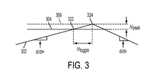
- FIG. 3 is a graph illustrating estimation of an inductance value in a boost converter according to one embodiment of the disclosure.
- the controller 222 may determine the transition time from the first time period to the second time period when the NFET 206 turns off and the PFET 208 turns on based on when the measured current, I boost , shown as line 302 crosses either a slope-compensated signal or a fixed upper limit shown as line 304 . After the controller 222 decides to toggle the NFET 206 and the PFET 208 , control signals from the controller 222 propagate through the level shifters and drivers 214 before driving the gates of the NFET 206 and PFET 208 .
- ⁇ t toggle the inductor current, I boost , continues to rise, which causes an error in the peak-current, ⁇ I peak , detected by the current mirror 218 .
- This error value may be computed as a difference between the inductor current, shown in line 302 , at the time of the control signal generation, indicated as cross point 322 and the actual value of the inductor current when the NFET 206 and the PFET 208 actually switch at point 324 .
- the up-slope of the inductor current of line 302 may be defined by
- ⁇ ⁇ ⁇ I peak ( K CM * V P L BOOST ) * ⁇ ⁇ ⁇ t toggle .
- ⁇ I peak is directly affected by the value of L boost .
- the error injected by ⁇ I peak may be calculated and calibrated out if the value of L boost is known.
- an amount of slope-compensation of line 304 for stability may be calculated as approximately at least half the down-slope of the line 302 , given by
- L boost varies, a variation in the slope compensation may occur, which could lead to insufficient slope compensation and instability due to, for example, sub-harmonic oscillation.
- the L boost value may be determined by the controller 222 and used to improve the slope-compensation. Without an L boost value, a worst-case slope compensation value may be used that is not optimal for many operating conditions. Additionally, if the controller 222 recognizes that the value of L boost is decreasing, the controller 222 may adjust slope-compensation to counter the effect of an increased slope-compensation requirement.
- Changes in L boost with changing inductor current may thus be compensated for by calculating the L boost value, knowing a starting value of L boost , calibrating its effect out initially, and then comparing a slope of the line 302 with a calculated value of the slope.
- changes in L boost such as due to variations in current and operation at or near saturation, may be compensated.
- an inductance L boost estimator may be integrated with the controller 222 , to improve slope-compensation calculation, which may improve system stability, and to accurately determine peak current, which may improve absolute current accuracy and may prevent the inductor 204 from operating in saturation.
- An initial calibration may be performed to determine when calculated inductance values, L boost , change.
- a known value of current may be forced through the inductor 204 and through the NFET 206 , and thus through the current mirror 218 .
- This known value of current may be used by the controller 222 to calibrate the current ADC 216 and the current mirror 218 .
- the boost converter may be operated with no load while samples of the current ADC 216 are taken by the controller 222 to establish a baseline inductance value from
- L BOOST VP / ( d ⁇ ⁇ i d ⁇ ⁇ t ) , where di is the difference between the current ADC 216 samples, and dt is the sampling period of the ADC 216 .
- An initial ⁇ I peak and slope compensation value may be calculated from these initial measurements and stored by the controller 222 .
- this baseline L boost value may be repeatedly compared with newly-calculated values of L boost .
- a change between the current value of L boost and the initial value of L boost may cause the controller 222 to update ⁇ I peak and the slope compensation values as described in the calculations above.
- the controller 222 may detect when saturation occurs and prevent saturation by reducing the current load, and consequently the current draw, thereby bringing the inductor 204 out of saturation and back into linear operation.
- FIG. 4 is a flow chart illustrating a method of estimating an inductance value and modifying boost converter operation in response to changes in inductance value according to one embodiment of the disclosure.
- a method 400 may begin at block 402 with obtaining an initial inductance value of an inductor of a boost converter. Block 402 may be performed, for example, during a start-up procedure before audio is output from an audio amplifier.
- a current through the inductor is measured by the controller during operation of the boost converter, such as while the boost converter and audio amplifier are amplifying an audio signal.
- an updated inductance value for the inductor of the boost converter may be determined by the controller based on the measured current of block 404 .
- the updated inductance value may indicate changes in the inductance value that are caused by, for example, operation at or near saturation or other conditions.
- an updated slope compensation value may be calculated for the updated inductance value of block 406 .
- the updated slope compensation value may be calculated from
- the updated slope compensation value of block 408 may be applied, at block 410 , to determine when to toggle charging and discharging of the inductor. For example, the controller may calculate an approximate time the current through the inductor will reach a peak current level by calculating a toggle delay in toggling the NFET and PFET of the boost converter. The controller may then toggle the NFET and PFET in advance of the time the inductor would reaches the peak current level, taking into account the toggle delay, to reduce damage to the inductor and undesirable effects output by the audio amplifier when saturation is reached.
- the method 400 executing in the controller may return to block 404 to repeatedly, continuously, periodically, or occasionally measure a current through the inductor and update the calculated inductance value at block 406 and slope compensation value at block 408 .
- an initial calibration and storage of the inductance, L boost in conjunction with periodic or occasional re-evaluation of the inductance value, L boost , by using, for example, the measured supply voltage, V P , by the ADC 212 and the measured boost current by the ADC 216 allows the controller 222 to monitor changes in the inductance value, L boost .
- a sudden drop in this value such as approximately a 30 to 80% change, may be indicative of reaching saturation or sudden inductor current spiking, which may cause damage to the inductor 204 and/or the boost converter.
- This information may be used by the controller 222 to control the audio amplifier and/or the boost converter to reduce the load and prevent damage to both the inductor and the boost converter.
- the controller 222 may dynamically adjust slope compensation to better stabilize the system, as well as increasing the accuracy of detected peak inductor current levels. For example, slope compensation may be adjusted between approximately ⁇ 70 and +80 percent during a span of approximately 3-10 microseconds.
- Computer-readable media includes physical computer storage media.
- a storage medium may be any available medium that can be accessed by a computer.
- such computer-readable media can comprise RAM, ROM, EEPROM, CD-ROM or other optical disk storage, magnetic disk storage or other magnetic storage devices, or any other medium that can be used to store desired program code in the form of instructions or data structures and that can be accessed by a computer.
- Disk and disc includes compact discs (CD), laser discs, optical discs, digital versatile discs (DVD), floppy disks and blu-ray discs. Generally, disks reproduce data magnetically, and discs reproduce data optically. Combinations of the above should also be included within the scope of computer-readable media.
- instructions and/or data may be provided as signals on transmission media included in a communication apparatus.
- a communication apparatus may include a transceiver having signals indicative of instructions and data. The instructions and data are configured to cause one or more processors to implement the functions outlined in the claims.
Landscapes
- Engineering & Computer Science (AREA)
- Power Engineering (AREA)
- Physics & Mathematics (AREA)
- General Physics & Mathematics (AREA)
- Theoretical Computer Science (AREA)
- Microelectronics & Electronic Packaging (AREA)
- Multimedia (AREA)
- General Engineering & Computer Science (AREA)
- Dc-Dc Converters (AREA)
- Amplifiers (AREA)
Abstract
Description
and a down-slope of the inductor current of
where Lboost is the inductance value, and KCM is the gain value of the current measurement path including the
where VP and Vbst are measured and provided to the
where di is the difference between the
wherein KCM is a gain value, Vbst is the boost voltage, VP is a supply voltage, and Lboost is the inductance value of the inductor.
Claims (16)
0.5*K CM*(V bst −V P)/L boost,
0.5*K CM*(V bst −V P)/L boost,
0.5*K CM*(V bst −V P)/L boost,
0.5*K CM*(V bst −V P)/L boost,
Priority Applications (4)
| Application Number | Priority Date | Filing Date | Title |
|---|---|---|---|
| US14/182,850 US9912312B2 (en) | 2013-07-26 | 2014-02-18 | Boost converter controller with inductance value determination |
| GB1600931.8A GB2529994B (en) | 2013-07-26 | 2014-07-22 | Boost converter controller with inductance value determination |
| CN201480041891.3A CN105474524B (en) | 2013-07-26 | 2014-07-22 | Method, electrical device and integrated circuit for boost converter |
| PCT/US2014/047624 WO2015013277A1 (en) | 2013-07-26 | 2014-07-22 | Boost converter controller with inductance value determination |
Applications Claiming Priority (2)
| Application Number | Priority Date | Filing Date | Title |
|---|---|---|---|
| US201361858939P | 2013-07-26 | 2013-07-26 | |
| US14/182,850 US9912312B2 (en) | 2013-07-26 | 2014-02-18 | Boost converter controller with inductance value determination |
Publications (2)
| Publication Number | Publication Date |
|---|---|
| US20150032396A1 US20150032396A1 (en) | 2015-01-29 |
| US9912312B2 true US9912312B2 (en) | 2018-03-06 |
Family
ID=52390561
Family Applications (6)
| Application Number | Title | Priority Date | Filing Date |
|---|---|---|---|
| US14/182,939 Active 2035-01-31 US9912238B1 (en) | 2013-07-26 | 2014-02-18 | Determination of inductor current during reverse current in a boost converter |
| US14/183,096 Active US9768689B1 (en) | 2013-07-26 | 2014-02-18 | Controller for imposing current limits on a boost converter for managing thermal loads |
| US14/182,798 Active 2034-08-08 US9520782B2 (en) | 2013-07-26 | 2014-02-18 | Boost converter voltage controlled based on audio signal |
| US14/182,850 Active 2035-12-02 US9912312B2 (en) | 2013-07-26 | 2014-02-18 | Boost converter controller with inductance value determination |
| US14/183,149 Active US9391517B1 (en) | 2013-07-26 | 2014-02-18 | Controller for adjusting a switching frequency in a boost converter |
| US15/350,431 Active US9742370B2 (en) | 2013-07-26 | 2016-11-14 | Boost converter voltage controlled based on audio signal |
Family Applications Before (3)
| Application Number | Title | Priority Date | Filing Date |
|---|---|---|---|
| US14/182,939 Active 2035-01-31 US9912238B1 (en) | 2013-07-26 | 2014-02-18 | Determination of inductor current during reverse current in a boost converter |
| US14/183,096 Active US9768689B1 (en) | 2013-07-26 | 2014-02-18 | Controller for imposing current limits on a boost converter for managing thermal loads |
| US14/182,798 Active 2034-08-08 US9520782B2 (en) | 2013-07-26 | 2014-02-18 | Boost converter voltage controlled based on audio signal |
Family Applications After (2)
| Application Number | Title | Priority Date | Filing Date |
|---|---|---|---|
| US14/183,149 Active US9391517B1 (en) | 2013-07-26 | 2014-02-18 | Controller for adjusting a switching frequency in a boost converter |
| US15/350,431 Active US9742370B2 (en) | 2013-07-26 | 2016-11-14 | Boost converter voltage controlled based on audio signal |
Country Status (4)
| Country | Link |
|---|---|
| US (6) | US9912238B1 (en) |
| CN (1) | CN105474524B (en) |
| GB (1) | GB2529994B (en) |
| WO (1) | WO2015013277A1 (en) |
Families Citing this family (36)
| Publication number | Priority date | Publication date | Assignee | Title |
|---|---|---|---|---|
| DE102013220596A1 (en) * | 2013-10-11 | 2015-04-16 | Continental Automotive Gmbh | Driver circuit for an inductance, method for operating an inductance and active transmitting device with a driver circuit |
| EP3103194B1 (en) | 2014-02-04 | 2018-11-28 | Cirrus Logic, Inc. | Switch mode amplifier |
| WO2015171931A1 (en) | 2014-05-08 | 2015-11-12 | Cirrus Logic, Inc. | System with multiple signal loops and switched mode converter |
| US9431894B2 (en) * | 2014-08-29 | 2016-08-30 | Nxp B.V. | Inductance variation based compensation in boost converter |
| US10021084B2 (en) * | 2014-10-28 | 2018-07-10 | Open Text Sa Ulc | Systems and methods for credentialing of non-local requestors in decoupled systems utilizing a domain local authenticator |
| US9628033B2 (en) | 2014-10-29 | 2017-04-18 | Cirrus Logic, Inc. | Power stage with switched mode amplifier and linear amplifier |
| WO2017027393A1 (en) | 2015-08-07 | 2017-02-16 | Cirrus Logic International Semiconductor, Ltd. | Adjusting peak inductor current to limit supply input current |
| CN108141134B (en) * | 2015-08-07 | 2020-11-13 | 思睿逻辑国际半导体有限公司 | Adjust Peak Inductor Current to Limit Supply Input Current |
| US10021485B2 (en) | 2015-11-17 | 2018-07-10 | Cirrus Logic, Inc. | Prevention of signal clipping due to decrease in amplifier supply voltage |
| US10601373B2 (en) * | 2016-03-31 | 2020-03-24 | Tymphany Hk Limited | Booster circuit including dynamically sliding power supply unit |
| US11075605B2 (en) | 2016-05-25 | 2021-07-27 | Cirrus Logic, Inc. | Dual-domain power distribution system in a mobile device |
| US12107551B2 (en) | 2016-05-25 | 2024-10-01 | Cirrus Logic Inc. | Dual-domain power distribution system in a mobile device |
| US10530303B2 (en) | 2016-05-25 | 2020-01-07 | Cirrus Logic, Inc. | Multi-phase power converter system using multiple amplifier integrated circuits |
| US10164535B2 (en) * | 2016-11-23 | 2018-12-25 | Texas Instruments Incorporated | Cycle-by-cycle peak current limiting in current mode buck/boost converters |
| GB2560045B (en) | 2017-02-28 | 2019-10-30 | Cirrus Logic Int Semiconductor Ltd | Amplifiers |
| CN106950431B (en) * | 2017-03-30 | 2019-04-12 | 华中科技大学 | The acquisition methods of reactor inductance under a kind of frequency domain |
| KR102300544B1 (en) * | 2017-04-07 | 2021-09-09 | (주)드림어스컴퍼니 | Modularized Signal Converting Apparatus and Method thereof |
| US10326405B2 (en) | 2017-05-18 | 2019-06-18 | Qualcomm Incorporated | Class-H switching amplifier circuit having supply voltage proportional to an audio signal |
| GB2578033B (en) * | 2017-05-22 | 2022-03-02 | Cirrus Logic Int Semiconductor Ltd | A DC-DC converter |
| DE102017209067A1 (en) * | 2017-05-30 | 2018-12-06 | Robert Bosch Gmbh | Class D amplifier and operating method |
| WO2019161867A1 (en) * | 2018-02-22 | 2019-08-29 | Aalborg Universitet | A two-terminal active inductor device |
| US10609477B1 (en) * | 2018-10-08 | 2020-03-31 | Texas Instruments Incorporated | Control system for regulation of boosted audio amplifier |
| US11728779B2 (en) * | 2019-01-18 | 2023-08-15 | Cirrus Logic Inc. | Signal tracking-based supply voltage generation with over-boosted voltage |
| JP7243241B2 (en) * | 2019-02-04 | 2023-03-22 | 富士電機株式会社 | Drive signal generation circuit, power supply circuit |
| US11205961B2 (en) * | 2019-04-15 | 2021-12-21 | Texas Instruments Incorporated | Hysteretic boost converter with inductor peak current gear-shifting |
| US11444577B2 (en) | 2019-06-07 | 2022-09-13 | Samsung Electronics Co., Ltd. | Boost amplifier |
| US10788523B1 (en) * | 2019-06-14 | 2020-09-29 | Infineon Technologies Ag | Inductor value determination for power converter |
| US11340296B2 (en) * | 2019-06-25 | 2022-05-24 | Motorola Mobility Llc | Electronic device with solid state switch monitoring |
| GB2591790B (en) * | 2020-02-06 | 2022-04-06 | Lithe Audio Ltd | Speaker system |
| US11563375B2 (en) * | 2021-02-02 | 2023-01-24 | Airoha Technology Corp. | Method and scheme capable of mitigating effect caused by occurrence of unexpected magnetic field/coupling for DC/DC power converter |
| CN113271061B (en) * | 2021-04-21 | 2023-02-10 | 华为数字能源技术有限公司 | Photovoltaic system, power converter and method for measuring inductance value |
| US11843317B2 (en) | 2021-08-25 | 2023-12-12 | Cirrus Logic Inc. | Pseudo-bypass mode for power converters |
| WO2023027837A1 (en) * | 2021-08-25 | 2023-03-02 | Cirrus Logic International Semiconductor Ltd. | Pseudo-bypass mode for power converters |
| US11876493B2 (en) * | 2022-02-04 | 2024-01-16 | Qualcomm Incorporated | Hybrid class-H/predictive class-G switching amplifier architecture |
| CN115378370B (en) * | 2022-10-21 | 2023-03-31 | 荣耀终端有限公司 | Audio amplification circuit, board card and electronic equipment |
| EP4645688A1 (en) | 2024-04-29 | 2025-11-05 | Goodix Technology (HK) Company Limited | Apparatus and method for adaptive boost voltage adjustment in dc-dc boost converter |
Citations (24)
| Publication number | Priority date | Publication date | Assignee | Title |
|---|---|---|---|---|
| US6087816A (en) * | 1999-06-29 | 2000-07-11 | Maxim Integrated Products, Inc. | Step-up/step-down switching regulators and pulse width modulation control therefor |
| US20050168198A1 (en) | 2004-02-02 | 2005-08-04 | The Regents Of The University Of Colorado, A Body Corporate | Predictive digital current controllers for switching power converters |
| US6952093B1 (en) | 2003-11-07 | 2005-10-04 | National Semiconductor Corporation | Adaptive small-signal compensation for switching regulators |
| US20060284607A1 (en) * | 2005-06-16 | 2006-12-21 | Yuji Isobe | Slope compensation circuit |
| US20090010035A1 (en) | 2007-07-06 | 2009-01-08 | Advanced Analogic Technologies, Inc. | Boost and up-down switching regulator with synchronous freewheeling MOSFET |
| US20090054023A1 (en) | 2007-08-24 | 2009-02-26 | Bean Ronnie A | Audio amplifier and methods of generating audio signals |
| US7737668B2 (en) | 2007-09-07 | 2010-06-15 | Panasonic Corporation | Buck-boost switching regulator |
| US20110018507A1 (en) * | 2009-07-22 | 2011-01-27 | Mccloy-Stevens Mark | Switched power regulator |
| US7898825B2 (en) | 2008-03-24 | 2011-03-01 | Akros Silicon, Inc. | Adaptive ramp compensation for current mode-DC-DC converters |
| US20110109283A1 (en) | 2008-06-06 | 2011-05-12 | Infineon Technologies Austria Ag | System and method for controlling a converter |
| US20110115458A1 (en) | 2009-09-18 | 2011-05-19 | Schafmeister Frank | Digital slope compensation for current mode control |
| US20110199062A1 (en) * | 2007-08-20 | 2011-08-18 | Austriamicrosystems Ag | DC/DC Converter Arrangement and Method for DC/DC Conversion |
| US20120182001A1 (en) | 2011-01-17 | 2012-07-19 | Immense Advance Technology Corp. | Low input voltage boost converter operable at low temperatures and boost controller thereof |
| US20120274295A1 (en) * | 2011-04-29 | 2012-11-01 | Energy Pass, Inc. | Current mode buck-boost converter |
| US20130057529A1 (en) | 2011-09-06 | 2013-03-07 | Kyuho LEE | Mobile terminal and power management unit thereof |
| US20130069613A1 (en) | 2011-09-21 | 2013-03-21 | Renesas Electronics Corporation | Dc/dc converter |
| US20130100711A1 (en) * | 2011-04-20 | 2013-04-25 | Nxp B.V. | Switching Circuit |
| US20130127530A1 (en) | 2011-11-22 | 2013-05-23 | Analog Devices, Inc. | Multi-level boosted class d amplifier |
| US8525502B2 (en) | 2011-03-02 | 2013-09-03 | Exar Corporation | Digital pulse-frequency modulation controller for switch-mode power supplies with frequency targeting and ultrasonic modes |
| US20130257533A1 (en) | 2012-04-03 | 2013-10-03 | Nxp B.V. | Switched-mode power supply and method of operation |
| US20140070728A1 (en) * | 2012-09-07 | 2014-03-13 | Infineon Technologies Austria Ag | Circuit and Method for Driving LEDs |
| US20140125303A1 (en) | 2012-11-02 | 2014-05-08 | Intersil Americas LLC | Limiting a current |
| US20140270240A1 (en) | 2013-03-15 | 2014-09-18 | Jay Solomon | Boost-on-demand amplifier |
| US20140347027A1 (en) | 2013-05-23 | 2014-11-27 | Micrel, Inc. | Optimal ripple injection for a boost regulator |
Family Cites Families (1)
| Publication number | Priority date | Publication date | Assignee | Title |
|---|---|---|---|---|
| JP2012253953A (en) * | 2011-06-06 | 2012-12-20 | Mitsumi Electric Co Ltd | Step-up dc-dc converter |
-
2014
- 2014-02-18 US US14/182,939 patent/US9912238B1/en active Active
- 2014-02-18 US US14/183,096 patent/US9768689B1/en active Active
- 2014-02-18 US US14/182,798 patent/US9520782B2/en active Active
- 2014-02-18 US US14/182,850 patent/US9912312B2/en active Active
- 2014-02-18 US US14/183,149 patent/US9391517B1/en active Active
- 2014-07-22 GB GB1600931.8A patent/GB2529994B/en active Active
- 2014-07-22 WO PCT/US2014/047624 patent/WO2015013277A1/en not_active Ceased
- 2014-07-22 CN CN201480041891.3A patent/CN105474524B/en active Active
-
2016
- 2016-11-14 US US15/350,431 patent/US9742370B2/en active Active
Patent Citations (28)
| Publication number | Priority date | Publication date | Assignee | Title |
|---|---|---|---|---|
| US6087816A (en) * | 1999-06-29 | 2000-07-11 | Maxim Integrated Products, Inc. | Step-up/step-down switching regulators and pulse width modulation control therefor |
| US6952093B1 (en) | 2003-11-07 | 2005-10-04 | National Semiconductor Corporation | Adaptive small-signal compensation for switching regulators |
| US7265530B1 (en) * | 2003-11-07 | 2007-09-04 | National Semiconductor Corporation | Adaptive slope compensation for switching regulators |
| US20050168198A1 (en) | 2004-02-02 | 2005-08-04 | The Regents Of The University Of Colorado, A Body Corporate | Predictive digital current controllers for switching power converters |
| US20060284607A1 (en) * | 2005-06-16 | 2006-12-21 | Yuji Isobe | Slope compensation circuit |
| US7425819B2 (en) | 2005-06-16 | 2008-09-16 | Microsemi Corporation | Slope compensation circuit |
| US20090010035A1 (en) | 2007-07-06 | 2009-01-08 | Advanced Analogic Technologies, Inc. | Boost and up-down switching regulator with synchronous freewheeling MOSFET |
| US20110199062A1 (en) * | 2007-08-20 | 2011-08-18 | Austriamicrosystems Ag | DC/DC Converter Arrangement and Method for DC/DC Conversion |
| US20090054023A1 (en) | 2007-08-24 | 2009-02-26 | Bean Ronnie A | Audio amplifier and methods of generating audio signals |
| US7737668B2 (en) | 2007-09-07 | 2010-06-15 | Panasonic Corporation | Buck-boost switching regulator |
| US7898825B2 (en) | 2008-03-24 | 2011-03-01 | Akros Silicon, Inc. | Adaptive ramp compensation for current mode-DC-DC converters |
| US20110109283A1 (en) | 2008-06-06 | 2011-05-12 | Infineon Technologies Austria Ag | System and method for controlling a converter |
| US20110018507A1 (en) * | 2009-07-22 | 2011-01-27 | Mccloy-Stevens Mark | Switched power regulator |
| US20110115458A1 (en) | 2009-09-18 | 2011-05-19 | Schafmeister Frank | Digital slope compensation for current mode control |
| US8278899B2 (en) * | 2009-09-18 | 2012-10-02 | Det International Holding Limited | Digital slope compensation for current mode control |
| US20120182001A1 (en) | 2011-01-17 | 2012-07-19 | Immense Advance Technology Corp. | Low input voltage boost converter operable at low temperatures and boost controller thereof |
| US8525502B2 (en) | 2011-03-02 | 2013-09-03 | Exar Corporation | Digital pulse-frequency modulation controller for switch-mode power supplies with frequency targeting and ultrasonic modes |
| US20130100711A1 (en) * | 2011-04-20 | 2013-04-25 | Nxp B.V. | Switching Circuit |
| US20120274295A1 (en) * | 2011-04-29 | 2012-11-01 | Energy Pass, Inc. | Current mode buck-boost converter |
| US20130057529A1 (en) | 2011-09-06 | 2013-03-07 | Kyuho LEE | Mobile terminal and power management unit thereof |
| US20130069613A1 (en) | 2011-09-21 | 2013-03-21 | Renesas Electronics Corporation | Dc/dc converter |
| US20130127530A1 (en) | 2011-11-22 | 2013-05-23 | Analog Devices, Inc. | Multi-level boosted class d amplifier |
| US8643436B2 (en) * | 2011-11-22 | 2014-02-04 | Analog Devices, Inc. | Multi-level boosted Class D amplifier |
| US20130257533A1 (en) | 2012-04-03 | 2013-10-03 | Nxp B.V. | Switched-mode power supply and method of operation |
| US20140070728A1 (en) * | 2012-09-07 | 2014-03-13 | Infineon Technologies Austria Ag | Circuit and Method for Driving LEDs |
| US20140125303A1 (en) | 2012-11-02 | 2014-05-08 | Intersil Americas LLC | Limiting a current |
| US20140270240A1 (en) | 2013-03-15 | 2014-09-18 | Jay Solomon | Boost-on-demand amplifier |
| US20140347027A1 (en) | 2013-05-23 | 2014-11-27 | Micrel, Inc. | Optimal ripple injection for a boost regulator |
Non-Patent Citations (2)
| Title |
|---|
| Crump et al. ,TPA2013D1 Boost Converter Component Selection, 2009. * |
| International Search Report and Written Opinion dated Nov. 21, 2014, during examination of PCT/US2014/047624. |
Also Published As
| Publication number | Publication date |
|---|---|
| CN105474524A (en) | 2016-04-06 |
| US20150030183A1 (en) | 2015-01-29 |
| US9742370B2 (en) | 2017-08-22 |
| US20150032396A1 (en) | 2015-01-29 |
| WO2015013277A1 (en) | 2015-01-29 |
| GB2529994A (en) | 2016-03-09 |
| US20170063318A1 (en) | 2017-03-02 |
| US9912238B1 (en) | 2018-03-06 |
| GB2529994B (en) | 2018-04-25 |
| US9768689B1 (en) | 2017-09-19 |
| CN105474524B (en) | 2018-07-10 |
| GB201600931D0 (en) | 2016-03-02 |
| US9520782B2 (en) | 2016-12-13 |
| US9391517B1 (en) | 2016-07-12 |
Similar Documents
| Publication | Publication Date | Title |
|---|---|---|
| US9912312B2 (en) | Boost converter controller with inductance value determination | |
| CN106717022B (en) | Temperature monitoring of loudspeakers | |
| EP3047571B1 (en) | Systems and methods for detection of load impedance of a transducer device coupled to an audio device | |
| KR101754011B1 (en) | Method and devices for non-intrusive power monitoring | |
| US20210167687A1 (en) | Current sensing for valley current-controlled power converters | |
| US9780763B1 (en) | Method and apparatus for offset calibration of a multi-mode high-speed comparator | |
| CN114325419A (en) | DC signal measurement and battery formation/testing | |
| KR102828589B1 (en) | Calibrated biasing of sleep transistors in integrated circuits | |
| EP4238217B1 (en) | Calibrating a phase interpolator by amplifying timing differences | |
| US9306504B2 (en) | Waveform shaping for audio amplifiers | |
| US8035427B2 (en) | Signal generating apparatus capable of measuring trip point of power-up signal and method of measuring trip point of power-up signal using the same | |
| JP2008228029A (en) | Semiconductor integrated circuit | |
| US20170245072A1 (en) | Identification of a load with a search algorithm that controls application of signals to the load and a reference generator | |
| CN101395790B (en) | Improved window comparator with accurate levels for use in DC-DC converters | |
| US20170245073A1 (en) | Temperature compensation for load identification | |
| TW202215772A (en) | Bias voltage compensation circuit and bias voltage compensation method applied to signal processing circuit | |
| US9521712B1 (en) | Measurements of multiple external components through a single pin of an integrated circuit | |
| JP7665300B2 (en) | Current source and current generation method | |
| JP2010169631A (en) | Constant current circuit and tester | |
| CN114152797B (en) | Current sensor with automatic offset voltage adjustment | |
| KR101612739B1 (en) | Distance measurement apparatus and method utilizing time to digital converter having scalable resolution | |
| JP6330798B2 (en) | Music player | |
| US20260005658A1 (en) | Switching amplifier circuitry | |
| KR102180166B1 (en) | Method of forming a transducer controller and circuit therefor | |
| US9712906B1 (en) | Alternating current (AC) load identification technique using a search algorithm |
Legal Events
| Date | Code | Title | Description |
|---|---|---|---|
| AS | Assignment |
Owner name: CIRRUS LOGIC, INC., TEXAS Free format text: ASSIGNMENT OF ASSIGNORS INTEREST;ASSIGNORS:PAZHAYAVEETIL, ULLAS;MAY, JEFFREY;KAMATH, GAUTHAM;AND OTHERS;SIGNING DATES FROM 20140210 TO 20140221;REEL/FRAME:032285/0950 |
|
| STCF | Information on status: patent grant |
Free format text: PATENTED CASE |
|
| MAFP | Maintenance fee payment |
Free format text: PAYMENT OF MAINTENANCE FEE, 4TH YEAR, LARGE ENTITY (ORIGINAL EVENT CODE: M1551); ENTITY STATUS OF PATENT OWNER: LARGE ENTITY Year of fee payment: 4 |
|
| MAFP | Maintenance fee payment |
Free format text: PAYMENT OF MAINTENANCE FEE, 8TH YEAR, LARGE ENTITY (ORIGINAL EVENT CODE: M1552); ENTITY STATUS OF PATENT OWNER: LARGE ENTITY Year of fee payment: 8 |