US9899082B2 - Semiconductor memory device - Google Patents
Semiconductor memory device Download PDFInfo
- Publication number
- US9899082B2 US9899082B2 US15/261,810 US201615261810A US9899082B2 US 9899082 B2 US9899082 B2 US 9899082B2 US 201615261810 A US201615261810 A US 201615261810A US 9899082 B2 US9899082 B2 US 9899082B2
- Authority
- US
- United States
- Prior art keywords
- data
- memory
- memory cell
- write command
- write
- Prior art date
- Legal status (The legal status is an assumption and is not a legal conclusion. Google has not performed a legal analysis and makes no representation as to the accuracy of the status listed.)
- Active
Links
Images


Classifications
-
- G—PHYSICS
- G11—INFORMATION STORAGE
- G11C—STATIC STORES
- G11C13/00—Digital stores characterised by the use of storage elements not covered by groups G11C11/00, G11C23/00, or G11C25/00
- G11C13/0002—Digital stores characterised by the use of storage elements not covered by groups G11C11/00, G11C23/00, or G11C25/00 using resistive RAM [RRAM] elements
- G11C13/0021—Auxiliary circuits
- G11C13/0069—Writing or programming circuits or methods
-
- G—PHYSICS
- G11—INFORMATION STORAGE
- G11C—STATIC STORES
- G11C11/00—Digital stores characterised by the use of particular electric or magnetic storage elements; Storage elements therefor
- G11C11/02—Digital stores characterised by the use of particular electric or magnetic storage elements; Storage elements therefor using magnetic elements
- G11C11/16—Digital stores characterised by the use of particular electric or magnetic storage elements; Storage elements therefor using magnetic elements using elements in which the storage effect is based on magnetic spin effect
- G11C11/161—Digital stores characterised by the use of particular electric or magnetic storage elements; Storage elements therefor using magnetic elements using elements in which the storage effect is based on magnetic spin effect details concerning the memory cell structure, e.g. the layers of the ferromagnetic memory cell
-
- G—PHYSICS
- G11—INFORMATION STORAGE
- G11C—STATIC STORES
- G11C11/00—Digital stores characterised by the use of particular electric or magnetic storage elements; Storage elements therefor
- G11C11/02—Digital stores characterised by the use of particular electric or magnetic storage elements; Storage elements therefor using magnetic elements
- G11C11/16—Digital stores characterised by the use of particular electric or magnetic storage elements; Storage elements therefor using magnetic elements using elements in which the storage effect is based on magnetic spin effect
- G11C11/165—Auxiliary circuits
- G11C11/1675—Writing or programming circuits or methods
-
- G—PHYSICS
- G11—INFORMATION STORAGE
- G11C—STATIC STORES
- G11C11/00—Digital stores characterised by the use of particular electric or magnetic storage elements; Storage elements therefor
- G11C11/02—Digital stores characterised by the use of particular electric or magnetic storage elements; Storage elements therefor using magnetic elements
- G11C11/16—Digital stores characterised by the use of particular electric or magnetic storage elements; Storage elements therefor using magnetic elements using elements in which the storage effect is based on magnetic spin effect
- G11C11/165—Auxiliary circuits
- G11C11/1693—Timing circuits or methods
-
- G—PHYSICS
- G11—INFORMATION STORAGE
- G11C—STATIC STORES
- G11C13/00—Digital stores characterised by the use of storage elements not covered by groups G11C11/00, G11C23/00, or G11C25/00
- G11C13/0002—Digital stores characterised by the use of storage elements not covered by groups G11C11/00, G11C23/00, or G11C25/00 using resistive RAM [RRAM] elements
- G11C13/0021—Auxiliary circuits
- G11C13/0023—Address circuits or decoders
- G11C13/0026—Bit-line or column circuits
-
- G—PHYSICS
- G11—INFORMATION STORAGE
- G11C—STATIC STORES
- G11C13/00—Digital stores characterised by the use of storage elements not covered by groups G11C11/00, G11C23/00, or G11C25/00
- G11C13/0002—Digital stores characterised by the use of storage elements not covered by groups G11C11/00, G11C23/00, or G11C25/00 using resistive RAM [RRAM] elements
- G11C13/0021—Auxiliary circuits
- G11C13/0023—Address circuits or decoders
- G11C13/0028—Word-line or row circuits
-
- G—PHYSICS
- G11—INFORMATION STORAGE
- G11C—STATIC STORES
- G11C13/00—Digital stores characterised by the use of storage elements not covered by groups G11C11/00, G11C23/00, or G11C25/00
- G11C13/0002—Digital stores characterised by the use of storage elements not covered by groups G11C11/00, G11C23/00, or G11C25/00 using resistive RAM [RRAM] elements
- G11C13/0021—Auxiliary circuits
- G11C13/0061—Timing circuits or methods
-
- G—PHYSICS
- G11—INFORMATION STORAGE
- G11C—STATIC STORES
- G11C11/00—Digital stores characterised by the use of particular electric or magnetic storage elements; Storage elements therefor
- G11C11/02—Digital stores characterised by the use of particular electric or magnetic storage elements; Storage elements therefor using magnetic elements
- G11C11/16—Digital stores characterised by the use of particular electric or magnetic storage elements; Storage elements therefor using magnetic elements using elements in which the storage effect is based on magnetic spin effect
- G11C11/165—Auxiliary circuits
- G11C11/1673—Reading or sensing circuits or methods
-
- G—PHYSICS
- G11—INFORMATION STORAGE
- G11C—STATIC STORES
- G11C13/00—Digital stores characterised by the use of storage elements not covered by groups G11C11/00, G11C23/00, or G11C25/00
- G11C13/0002—Digital stores characterised by the use of storage elements not covered by groups G11C11/00, G11C23/00, or G11C25/00 using resistive RAM [RRAM] elements
- G11C13/0021—Auxiliary circuits
- G11C13/004—Reading or sensing circuits or methods
-
- G—PHYSICS
- G11—INFORMATION STORAGE
- G11C—STATIC STORES
- G11C13/00—Digital stores characterised by the use of storage elements not covered by groups G11C11/00, G11C23/00, or G11C25/00
- G11C13/0002—Digital stores characterised by the use of storage elements not covered by groups G11C11/00, G11C23/00, or G11C25/00 using resistive RAM [RRAM] elements
- G11C13/0021—Auxiliary circuits
- G11C13/0069—Writing or programming circuits or methods
- G11C2013/0085—Write a page or sector of information simultaneously, e.g. a complete row or word line
-
- G—PHYSICS
- G11—INFORMATION STORAGE
- G11C—STATIC STORES
- G11C13/00—Digital stores characterised by the use of storage elements not covered by groups G11C11/00, G11C23/00, or G11C25/00
- G11C13/0002—Digital stores characterised by the use of storage elements not covered by groups G11C11/00, G11C23/00, or G11C25/00 using resistive RAM [RRAM] elements
- G11C13/0021—Auxiliary circuits
- G11C13/0069—Writing or programming circuits or methods
- G11C2013/0088—Write with the simultaneous writing of a plurality of cells
-
- G—PHYSICS
- G11—INFORMATION STORAGE
- G11C—STATIC STORES
- G11C2213/00—Indexing scheme relating to G11C13/00 for features not covered by this group
- G11C2213/70—Resistive array aspects
- G11C2213/79—Array wherein the access device being a transistor
Definitions
- Embodiments described herein relate generally to a semiconductor memory device.
- a Magnetic Random Access Memory is a memory device which uses a storage element having a magnetoresistive effect on a memory cell for storing information.
- the MRAM is receiving attention as a next-generation memory device characterized by high-speed operation, large storage capacity, and non-volatility.
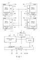
- FIG. 1 is a block diagram showing an entire structure of a semiconductor memory device according to a first embodiment.
- FIG. 2 shows a memory cell array of the semiconductor memory device according to the first embodiment.
- FIG. 3A is a cross-sectional view showing an outline configuration of a variable resistance element in the semiconductor memory device according to the first embodiment.
- FIG. 3B is a diagram to explain a write at the variable resistance element in the semiconductor memory device according to the first embodiment, and is a cross-sectional view of the variable resistance element in a P state.
- FIG. 3C is a diagram to explain a write at the variable resistance element in the semiconductor memory device according to the first embodiment, and is a cross-sectional view of the variable resistance element in an AP state.
- FIG. 4 is a block diagram showing the memory cell array and a read/write circuit in the semiconductor memory device according to the first embodiment.
- FIG. 5 is a timing chart showing a first example of the write at the semiconductor memory device according to the first embodiment.
- FIG. 6 is a timing chart showing a second example of the write at the semiconductor memory device according to the first embodiment.
- FIG. 7 is a timing chart showing a write at the semiconductor memory device according to a first comparative example.
- FIG. 8 is a timing chart showing a write at the semiconductor memory device according to a second comparative example.
- FIG. 9 is a timing chart showing a modification of the write at the semiconductor memory device according to the first embodiment.
- FIG. 10 is a timing chart showing a write at the semiconductor memory device according to a second embodiment.
- a semiconductor memory device includes: a first memory cell including a first variable resistance element; a first buffer coupled to the first memory cell; a second memory cell including a second variable resistance element; and a second buffer coupled to the second memory cell.
- first data is stored in the first buffer and is transferred to the first memory cell
- second data is stored in the second buffer and is transferred to the second memory cell
- a start of the transferring the first data and the second data is based on a first data transfer signal.
- FIGS. 1, 2, 3, 4, 5, 6, and 8 A semiconductor memory device according to a first embodiment will be explained in the following using FIGS. 1, 2, 3, 4, 5, 6, and 8 .
- an MRAM for storing data using a magnetoresistive effect element (an MTJ element) as a variable resistance element is explained as an example, but is not limited thereto.
- the present embodiment is applicable to any general memory (for example ReRAM or PCRAM) which senses a resistance difference between variable resistance elements by converting the resistance difference into a current difference or a voltage difference.
- the term “connect (couple)” should be construed to include not only a direct connection, but also a connection through any intervening element, unless otherwise mentioned in particular.
- one end of a transistor indicates one of a source or a drain, and the other end indicates one of the other source or drain.
- FIG. 1 is a block diagram showing the entire configuration of the semiconductor memory device (MRAM) according to the first embodiment.
- the semiconductor memory device comprises banks BK (BK 0 -BK 3 ), a data circuit 15 , a command/address circuit 16 , a controller 17 , and an input output circuit 18 .
- the bank BK 0 comprises a memory cell array 11 _ 0 , a row decoder 12 _ 0 , a read/write circuit 13 _ 0 , and a column decoder 14 _ 0 .
- Each of the banks BK 1 to BK 3 has the same configuration as the bank BK 0 , in other words, comprises memory cell arrays 11 _ 1 to 11 _ 3 , row decoders 12 _ 0 to 12 _ 3 , read/write circuits 13 _ 0 to 13 _ 3 , and column decoders 14 _ 0 to 14 _ 3 , respectively.
- the configuration of bank BK 0 will be explained as an example.
- the bank BK is the largest activation unit selectable from outside (unillustrated controller).
- FIG. 2 shows a memory cell array 11 _ 0 of the semiconductor memory device according to the first embodiment.
- bit lines BL (BL 0 to BL 3 ), source lines SL (SL 0 to SL 3 ), and word lines WL (WL 0 to WL 3 ).
- the bit lines BL and the source lines SL extend in a first direction, and are arranged alternately in a second direction which is orthogonal to the first direction.
- the word lines WL extend in the second direction.
- a memory cell array 10 comprises a plurality of memory cells MC. Each of the memory cells MC is provided at a position where the bit lines BL and the source lines SL intersect with the word lines WL.
- the plurality of memory cells MC are arrayed matrix-like in the first direction and the second direction.
- the bit line BL 0 and the source line SL 0 will be considered as column 0
- the bit line BL 1 and the source line SL 1 will be considered as column 1
- the bit line BL 2 and the source line SL 2 will be considered as column 2
- the bit line BL 3 and the source line SL 3 will be considered as column 3 .
- bit lines BL, source lines SL, and word lines WL in the memory cell array 11 _ 0 and the column are only an example, therefore, are not limited thereto.
- the memory cell MC includes, for example, a variable resistance element R and a select transistor ST.
- One end of the variable resistance element R is electrically coupled to bit line BL, and the other end thereof is electrically coupled to one end of the select transistor ST.
- the other end of the select transistor ST is electrically coupled to the source line SL, and the gate of the select transistor ST is electrically coupled to the word line WL.
- the variable resistance element R is an element whose resistance value varies by applying a current (or voltage).
- the variable resistance element R includes, for example, an MTJ element, a phase change element, and a ferroelectric element.
- the memory cell MC is selected when the select transistor ST is turned on by the word line WL.
- the MRAM is adopted, that is, the variable resistance element R is an MTJ element, will be explained.
- FIG. 3A is a cross-sectional view of an outline configuration of the variable resistance element R in the semiconductor memory device according to the first embodiment.
- a variable resistance element R a storage layer 31 , a tunnel barrier layer 32 , and a reference layer 33 are mainly presented.
- variable resistance element R comprises a laminated body comprised of the storage layer 31 which is a ferromagnetic layer, the reference layer 33 which is a ferromagnetic layer, and the tunnel barrier layer 32 which is a non-magnetic layer formed therebetween.
- the storage layer 31 is a ferromagnetic layer in which a magnetization direction is variable, and has perpendicular magnetic anisotropy which is perpendicular or almost perpendicular to a film surface (upper surface/lower surface).
- a variable magnetization direction means that a magnetization direction varies with respect to a predetermined write current.
- almost perpendicular means that a remanent magnetization direction falls within the range of 45 ⁇ 90 with respect to a film surface.
- the storage layer 31 is made of, for example, cobalt-iron-boron (CoFeB) or boronized iron (FeB).
- the tunnel barrier layer 32 is formed on the storage layer 31 .
- the tunnel barrier layer 32 is a non-magnetic layer, and is made of, for example, MgO.
- the reference layer 33 is formed on the tunnel barrier layer 32 .
- the reference layer 33 is a ferromagnetic layer in which a magnetization direction is not variable, and has perpendicular magnetic anisotropy which is perpendicular to or almost perpendicular to the film surface.
- a non-variable magnetization direction means that a magnetization direction does not vary with respect to a predetermined write current.
- the reference layer 33 has a greater inverted energy barrier in the magnetization direction than what the storage layer 31 has.
- the reference layer 33 is made of, for example, cobalt platinum (CoPt), cobalt nickel (CoNi), or cobalt palladium (CoPd).
- FIG. 3B is a diagram to explain a write at the variable resistance element R in the semiconductor memory device according to the first embodiment, and is a cross-sectional view of the variable resistance element in a parallel state (P state).
- FIG. 3C is a diagram to explain a write at the variable resistance element R in the semiconductor memory device according to the first embodiment, and is a cross-sectional view of the variable resistance element in an anti-parallel state (AP state).
- variable resistance element R is, for example, a spin injection type variable resistance element. Accordingly, when data is written to the variable resistance element R, or data is read from the variable resistance element R, a current is fed in both directions perpendicular to the film surface in the variable resistance element R.
- variable resistance element R More specifically, data is written to the variable resistance element R in the following manner.
- the magnetization direction of the storage layer 31 is adapted to the same direction as the magnetization direction of the reference layer 33 .
- the magnetization direction of the reference layer 33 and the magnetization direction of the storage layer 31 will be in a parallel arrangement.
- a resistance value of the variable resistance element R becomes the lowest. For example, this case is defined as “0” data.
- the magnetization direction of the storage layer 31 is adapted to a direction opposite to the magnetization direction of the reference layer 33 . Accordingly, the magnetization direction of the reference layer 33 and the magnetization direction of the storage layer 31 are in an anti-parallel arrangement. When in this anti-parallel state, the resistance value of the variable resistance element R becomes the highest. For example, this case is defined as “1” data.
- a read current is supplied to the variable resistance element R.
- This read current is set to a value at which the magnetization direction of the storage layer 31 would not be inverted (i.e., a value smaller than a write current).
- the row decoder 12 _ 0 selects the word line WL in accordance with a row address.
- the column decoder 14 _ 0 selects the bit line BL and the source line SL in accordance with a column address.
- the read/write circuit 13 _ 0 controls writing to the memory cell array 11 _ 0 and reading from the memory cell array 11 _ 0 .
- the read/write circuit 13 _ 0 includes elements such as a write driver, a page buffer, and a sense amplifier.
- the write driver in the write, applies a write voltage to the memory cell MC and feeds a write current.
- the sense amplifier in the read, senses the read current or the read voltage applied to the memory cell MC.
- the page buffer when writing and reading data, temporarily stores data in units of writing to the memory cell MC and data in units of reading from the memory cell MC.
- FIG. 4 is a block diagram showing the memory cell array 11 and the read/write circuit 13 in the semiconductor memory device according to the first embodiment.
- the page buffer is shown as the read/write circuit 13 .
- one memory cell MC is shown in each column.
- the memory cell array 11 _ 0 has a memory cell MC (MC 0 to MC 3 ) for each column (column 0 to column 3 ).
- the read/write circuit 13 _ 0 has a page buffer region 13 A.
- the page buffer region 13 A has a volatile page buffer PB (PB 0 to PB 3 ) for each column.
- Each of the page buffers PB 0 to PB 3 is electrically coupled to each of the memory cells MC 0 to MC 3 via each of switches SW 0 to SW 3 .
- Each of the page buffers PB 0 to PB 3 in the write, stores data DQ from the data circuit 15 .
- Each of the page buffers PB 0 to PB 3 transfers the data DQ to each of the memory cells MC 0 to MC 3 at a predetermined timing by setting each of the switches SW 0 to SW 3 on.
- the switches SW 0 to SW 3 turn on by using data transfer signal DT (a pulse or a rise) described later as a trigger.
- the input/output circuit 18 controls signals transmitted therebetween an external device (for example, a memory controller). More specifically, the input/output circuit 18 receives from the external device a command/address signal CA, data DQ, a data strobe signal DQS, and a clock CLK/CLKb. The input/output circuit 18 supplies the command and the address signal CA received from the external device to the command/address circuit 16 . The input/output circuit 18 transfers the data DQ received from the external device to the data circuit 15 . The input/output circuit 18 supplies various control signals to the controller 17 .
- an external device for example, a memory controller. More specifically, the input/output circuit 18 receives from the external device a command/address signal CA, data DQ, a data strobe signal DQS, and a clock CLK/CLKb. The input/output circuit 18 supplies the command and the address signal CA received from the external device to the command/address circuit 16 . The input/output circuit 18 transfers the data
- the command/address circuit 16 receives the command/address signal CA from the input/output circuit 18 , and supplies signals based on this to the banks BK 0 to BK 3 .
- the command/address circuit 16 receives the clocks CLK and CLKb from the input/output circuit 18 , and outputs various signals at a timing based on the clocks CLK and CLKb.
- the data circuit DQ receives the data DQ from the input/output circuit 18 , and transfers this to the banks BK 0 to BK 3 .
- the controller 17 includes elements such as a voltage generating circuit, and controls each constituent element based on the control signal from the input/output circuit 18 .
- FIG. 5 is a timing chart showing a first example of a write at the semiconductor memory device according to the first embodiment.
- the semiconductor memory device operates by receiving various commands based on the timing of the clock CLK/CLKb.
- an active command ACT is supplied to the semiconductor memory device.
- the active command ACT includes a bank address and a row address.
- the command/address circuit 16 activates a corresponding bank BK based on the bank address.
- the command/address circuit 16 transfers a row address to a row decoder 12 of the corresponding bank BK.
- a write command WT 0 is supplied to the semiconductor memory device.
- the write command WT 0 includes a column address (address of column 0 ).
- the command/address circuit 16 transfers the column address to a column decoder 13 of the corresponding bank BK.
- the data DQ 0 is supplied to the semiconductor memory device with the write command WT 0 .
- the data circuit 15 transfers the data DQ 0 to the page buffer PB 0 based on the timing of receiving the write command WTO.
- the write commands WT 1 to WT 3 are continuously supplied in sequence to the semiconductor memory device.
- the write commands WT 1 to WT 3 include column addresses (addresses of columns 1 to 3 ). Meanwhile, data DQ 1 to DQ 3 are supplied in sequence to the semiconductor memory device with the write commands WT 1 to WT 3 .
- the data circuit 15 transfers the data DQ 1 to the page buffer PB 1 based on the timing of receiving the write command WT 1 , transfers the data DQ 2 to the page buffer PB 2 based on the timing of receiving the write command WT 2 , and transfers the data DQ 3 to the page buffer PB 3 based on the timing of receiving the write command WT 3 .
- the command/address circuit 16 counts the number of clocks CLK/CLKb after the timing of receiving the write command WTO.
- the command/address circuit 16 sets a data transfer signal DT at H level for a short time (or an arbitrary time) (generates a pulse).
- the command/address circuit 16 sets the data transfer signal DT at H level. Based on this pulse of the data transfer signal DT, transferring the data DQ stored in the page buffer PB to the memory cell MC is started.
- each of the data DQ 0 to DQ 3 of the page buffers PB 0 to PB 3 is transferred to each of the memory cells MC 0 to MC 3 in parallel.
- the write command WT 3 is supplied to the semiconductor memory device.
- the data DQ 4 is supplied to the semiconductor memory device with the write command WT 3 .
- the data circuit 15 transfers the data DQ 4 to the page buffer PB 3 based on the timing of receiving the write command WT 3 .
- the data DQ 4 is new data written to the memory cell MC 3 .
- the write commands WT 2 to WT 0 are continuously supplied in sequence to the semiconductor memory device in a similar manner. Meanwhile, the data DQ 2 to DQ 0 are supplied to the semiconductor memory device in sequence with the write commands WT 2 to WT 0 .
- the data circuit 15 transfers the data DQ 2 to the page buffer PB 2 based on the timing of receiving the write command WT 2 , transfers the data DQ 1 to the page buffer PB 1 based on the timing of receiving the write command WT 1 , and transfers the data DQ 0 to the page buffer PB 0 based on the timing of receiving the write command WT 0 .
- the command/address circuit 16 counts the number of clocks CLK/CLKb after the timing of receiving the write command WT 3 for the second time.
- the command/address circuit 16 sets the data transfer signal DT at H level for a short time (generates a pulse). Based on this pulse of the data transfer signal DT, transferring the data DQ stored in the page buffer PB to the memory cell MC is started.
- each of the data DQ 4 to DQ 7 of the page buffers PB 3 to PB 0 is transferred to each of the memory cells MC 0 to MC 3 in parallel.
- a pre-charge command PCG is supplied to the semiconductor memory device.
- the command/address circuit 16 inactivates the corresponding bank BK based on the pre-charge command PCG.
- the pulse of the data transfer signal DT is generated, however, the number of clocks CLK/CLKb is not limited thereto.
- the number of clocks CLK/CLKb should be set so that the interval for generating the pulse of the data transfer signal DT (interval of transferring data to the memory cell MC (interval of a transfer completion of the previous data and a transfer start of the subsequent data)) is equal to or longer than a recovery time.
- the magnetization direction of the reference layer 33 of the memory cell MC is inverted temporarily by the write.
- a recovery time is a time in which the magnetization direction of the reference layer 33 of the memory cell MC is inverted by the write.
- the number of clocks CLK/CLKb is equal to the number of write commands WT, but is not limited thereto.
- one write command WT may be synchronized with two clocks CLK/CLKb.
- FIG. 6 is a timing chart showing a second example of a write at the semiconductor memory device according to the first embodiment.
- the second example shows a case in which a plurality of write commands WT 0 are supplied successively.
- the write command WT 0 (a first write command WT 0 ) is supplied.
- the first write command WT 0 includes a column address (an address of column 0 ).
- the data DQ 0 is supplied to the semiconductor memory device with the first write command WT 0 .
- the data circuit 15 transfers the data DQ 0 to the page buffer PB 0 based on the timing of receiving the first write command WT 0 .
- Three write commands WT 0 (a second write command WT 0 , a third write command WT 0 , and a fourth write command WT 0 ) are continuously supplied to the semiconductor memory device in sequence in a similar manner.
- the second write command WT 0 to the fourth write command WT 0 include column addresses (an address of column 0 ). Meanwhile, the data DQ 1 to DQ 3 are supplied in sequence to the semiconductor memory device with the second write command WT 0 to the fourth write command WT 0 .
- the data circuit 15 transfers the data DQ 1 to the page buffer PB 0 based on the timing of receiving the second write command WTO, transfers the data DQ 2 to the page buffer PB 0 based on the timing of receiving the third write command WTO, and transfers the data DQ 3 to the page buffer PB 0 based on the timing of receiving the third write command WTO.
- the page buffer PB 0 stores the data DQ 3 which was transferred last.
- the command/address circuit 16 counts the number of clocks CLK/CLKb after the timing of receiving the first write command WT 0 .
- the command/address circuit 16 sets the data transfer signal DT at H level for a short time (generates a pulse). Based on this data transfer signal DT, transferring the data DQ stored in the page buffer PB to the memory cell MC is started.
- the data DQ 3 of the page buffer PB 0 is transferred to the memory cell MC 0 .
- the write commands WT 3 to WT 0 are supplied to the semiconductor memory device in sequence.
- the data DQ (DQ 4 to DQ 7 ) are transferred to the memory cells MC (MC 3 to MC 0 ) in parallel.
- the pre-charge command PCG is supplied to the semiconductor memory device, and the corresponding bank BK is inactivated based on the pre-charge command PCG.
- the reference layer 33 and an unillustrated shift cancel layer form a synthetic antiferromagnet structure, in which the magnetization directions are opposite.
- the magnetization direction of the shift cancel layer causes the magnetization direction of the reference layer 33 to be inverted.
- the magnetization direction of the reference layer 33 is inverted again and returns to its original direction.
- a write is performed before the reference layer 33 returns to its original magnetization direction (before the recovery time passes after the write)
- erroneous writing occurs. An example of erroneous writing is explained in detail in the following.
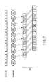
- FIG. 7 is a timing chart showing a write at the semiconductor memory device according to a first comparative example.
- the data circuit 15 transfers the data DQ 0 to the page buffer PB 0 based on the timing of receiving the write command WT 0 .
- the data DQ 0 transferred to the page buffer PB 0 is transferred continuously to the memory cell MC 0 .
- each of the data DQ transferred to the page buffers PB 1 to PB 3 is continuously transferred to each of the memory cells MC 1 to MC 3 .
- the data DQ 3 is transferred to the page buffer 3 , then transferred to the memory cell MC 3 continuously. Subsequently, after the data DQ 4 is transferred to the page buffer 3 , the data DQ 4 is transferred to the memory cell MC 3 continuously. In other words, the write to the memory cell MC 3 is performed twice, consecutively, in a short time. Therefore, as mentioned above, if the write of the data DQ 4 to the memory cell MC 3 is performed before the lapse of recovery time after the write of the data DQ 3 , erroneous writing occurs.
- a method of transferring the data DQ of all of the page buffers PB in parallel to the memory cell MC based on, for example, the pre-charge command PCG supplied last may be considered.
- the write current increases, i.e., causing power-supply noise to increase and causing a writing failure.
- the data DQ is transferred to each of the page buffers PB 0 to PB 3 based on the timing of the write commands WTO to WT 3 received in sequence.
- the data DQ of each of the page buffers PB 0 to PB 3 is transferred in parallel to each of the memory cells MC 0 to MC 3 based on the pulse of the data transfer signal DT.
- the pulse of the data transfer signal DT is based on the number of clocks CLK/CLKb and indicates the timing at which the data DQ has been transferred to a predetermined nth page buffer PB (in FIG. 5 , the fourth page buffer PB 3 ).
- FIG. 8 is a timing chart showing a write at the semiconductor memory device according to a second comparative example.
- the data circuit 15 transfers the data DQ to the page buffer PB 0 based on the timing of receiving a first write command WT 0 .
- the data DQ 0 transferred to the page buffer PB 0 is transferred continuously to the memory cell MC 0 .
- the data circuit 15 transfers the data DQ 1 to the page buffer PB 0 and the memory cell MC 0 based on the timing of receiving a second write command WT 0 , transfers the data DQ 2 to the page buffer PB 0 and the memory cell MC 0 based on the timing of receiving a third write command WT 0 , and transfers the data DQ 3 to the page buffer PB 0 and the memory cell MC 0 based on the timing of receiving a fourth write command WT 0 . Finally, the data DQ 3 is written on the memory cell MC 0 .
- the write to the memory cell MC 0 is performed the number of times equal to the number of the write commands WT 0 . Therefore, the number of writes to the memory cell MC 0 increases, deteriorating the reliability of the memory cell MC 0 .
- the data DQ (DQ 0 , DQ 1 , DQ 2 , DQ 3 ) is transferred to the page buffer PB 0 based on the timing of the write command WT 0 received in sequence (first write command WT 0 , second write command WT 0 , third write command WT 0 , fourth write command WT 0 ).
- the page buffer PB 0 stores the data DQ 3 transferred last.
- the data DQ 3 of the page buffer PB 0 is transferred to the memory cell MC 0 .
- the number of writes (the number of transfers) to the same memory cell MC may be reduced. In this manner, deterioration in the reliability of the memory cell MC may be suppressed.
- FIG. 9 is a timing chart showing a modified example of the write operation of the semiconductor memory device according to the first embodiment.
- a first data transfer signal DT 1 and a second data transfer signal DT 2 are generated.
- the data DQ is transferred to the memory cell MC not based on the pulses thereof but based on a rise to an H level.
- the modification will be explained in detail below.
- a write command WT 0 (a first write command WT 0 ) is supplied.
- the first write command WT 0 includes a column address (an address of column 0 ).
- data DQ 0 is supplied to the semiconductor memory device with the first write command WT 0 .
- the data circuit 15 transfers the data DQ 0 to a page buffer PB 0 based on the timing of receiving the first write command WT 0 .
- write commands WT 1 to WT 3 are supplied to the semiconductor memory device in sequence.
- the write commands WT 1 to WT 3 include a column address (addresses of columns 1 to 3 ).
- data DQ 1 to DQ 3 are supplied to the semiconductor memory device with the write commands WT 1 to WT 3 .
- the data circuit 15 transfers the data DQ 1 to a page buffer PB 1 based on the timing of receiving the write command WT 1 , transfers the data DQ 2 to a page buffer PB 2 based on the timing of receiving the write command WT 2 , and transfers the data DQ 3 to a page buffer PB 3 based on the timing of receiving the write command WT 3 .
- the command/address circuit 16 counts the number clocks CLK/CLKb thereafter the timing of receiving the write command WT 0 .
- the command/address circuit 16 sets the first data transfer signal DT 1 to the H level.
- the command/address circuit 16 sets the first data transfer signal DT 1 to the H level.
- the data DQ stored in the page buffer PB starts to be transferred to the memory cell MC.
- each of the data DQ 0 to DQ 3 of the page buffers PB 0 to PB 3 is transferred to each of the memory cells MC 0 to MC 3 in parallel.
- the write command WT 3 is supplied to the semiconductor memory device.
- data DQ 4 is supplied to the semiconductor memory device with the write command WT 3 .
- the data circuit 15 transfers the data DQ 4 to the page buffer PB 3 based on the timing of receiving the write command WT 3 .
- the write commands WT 2 to WT 0 are supplied to the semiconductor memory device in sequence. Meanwhile, the data DQ 2 to DQ 0 are supplied to the semiconductor memory device with the write commands WT 2 to WT 0 .
- the data circuit 15 transfers the data DQ 2 to the page buffer PB 2 based on the timing of receiving the write command WT 2 , transfers the data DQ 1 to a page buffer PB 1 based on the timing of receiving the write command WT 1 , and transfers the data DQ 0 to a page buffer PB 0 based on the timing of receiving the write command WT 0 .
- the command/address circuit 16 counts the number of clocks CLK/CLKb thereafter the timing of receiving the second write command WT 3 .
- the command/address circuit 16 sets the second data transfer signal DT 2 to the H level. Based on the rise of this second data transfer signal DT 2 , the data DQ stored in the page buffer PB starts to be transferred to the memory cell MC.
- each of the data DQ 4 to DQ 7 of the page buffers PB 3 to PB 0 is transferred to each of the memory cells MC 3 to MC 0 in parallel.
- a pre-charge command PCG is supplied to the semiconductor memory device.
- the command/address circuit 16 inactivates a corresponding bank BK based on the pre-charge command PCG.
- FIG. 10 will be used to explain a semiconductor memory device according to a second embodiment.
- the second embodiment is different from the above first embodiment in that a pulse of a data transfer signal DT is generated based on the number of write commands WT.
- FIG. 10 is a timing chart showing a write at the semiconductor memory device according to the second embodiment.
- the write command WT 0 is supplied to the semiconductor memory device.
- the write command WT 0 includes a column address (an address of column 0 ).
- the data DQ 0 is supplied to the semiconductor memory device with the write command WT 0 .
- the data circuit 15 transfers the data DQ 0 to the page buffer PB 0 based on the timing of receiving the write command WT 0 .
- the write command WT 1 is continuously supplied to the semiconductor memory device.
- the data DQ 1 is supplied to the semiconductor memory device with the write command WT 1 .
- the data circuit 15 transfers the data DQ 1 to the page buffer PB 1 based on the timing of receiving the write command WT 1 .
- the write commands WT 2 to WT 3 are supplied to the semiconductor memory device.
- the data DQ 2 to DQ 3 are supplied to the semiconductor memory device with the write commands WT 2 to WT 3 .
- the data circuit 15 transfers the data DQ 2 to the page buffer PB 2 based on the timing of receiving the write command WT 2 , and transfers the data DQ 3 to the page buffer PB 3 based on the timing of receiving the write command WT 3 .
- the command/address circuit 16 counts the number of write commands WT after the timing of receiving the write command WT 0 .
- the command/address circuit 16 sets a data transfer signal DT at H level for a short time (generates a pulse).
- the command/address circuit 16 sets the data transfer signal DT at H level when four write commands WT are received.
- transferring the data DQ stored in the page buffer PB to the memory cell MC is started.
- each of the data DQ 0 to DQ 3 of the page buffers PB 0 to PB 3 is transferred to each of the memory cells MC 0 to MC 3 in parallel.
- the write commands WT 3 to WT 0 are supplied to the semiconductor memory device in sequence.
- the data DQ (DQ 4 to DQ 7 ) is transferred to the memory cells MC (MC 3 to MC 0 ) in parallel.
- the pre-charge command PCG is supplied to the semiconductor memory device, and the corresponding bank BK is inactivated based on the pre-charge command PCG.
- the data transfer signal DT is generated.
- the number of write commands WT is not limited thereto.
- the number of write commands WT should be set so that the interval for generating pulse of the data transfer signal DT (the interval of transferring data to the memory cell MC) is equal to or longer than the recovery time.
- the second embodiment can produce the same effect as the first embodiment.
- each of the data DQ of the page buffers PB 0 to PB 3 is transferred in parallel to each of the memory cells MC 0 to MC 3 based on the pulse of the data transfer signal DT.
- the pulse of the data transfer signal DT is based on the number of write commands WT and indicates the timing at which the data DQ has been transferred to a predetermined nth page buffer PB (herein, the fourth page buffer PB 3 ).
- the write characteristic may be made constant, which would facilitate write control.
- the number of writes to the same memory cell MC (the number of transfers) can be further reduced. In this manner, deterioration in the reliability of the memory cell MC may be suppressed.
Landscapes
- Engineering & Computer Science (AREA)
- Computer Hardware Design (AREA)
- Mram Or Spin Memory Techniques (AREA)
Abstract
Description
Claims (10)
Priority Applications (1)
| Application Number | Priority Date | Filing Date | Title |
|---|---|---|---|
| US15/261,810 US9899082B2 (en) | 2016-03-03 | 2016-09-09 | Semiconductor memory device |
Applications Claiming Priority (2)
| Application Number | Priority Date | Filing Date | Title |
|---|---|---|---|
| US201662303335P | 2016-03-03 | 2016-03-03 | |
| US15/261,810 US9899082B2 (en) | 2016-03-03 | 2016-09-09 | Semiconductor memory device |
Publications (2)
| Publication Number | Publication Date |
|---|---|
| US20170256313A1 US20170256313A1 (en) | 2017-09-07 |
| US9899082B2 true US9899082B2 (en) | 2018-02-20 |
Family
ID=59722815
Family Applications (1)
| Application Number | Title | Priority Date | Filing Date |
|---|---|---|---|
| US15/261,810 Active US9899082B2 (en) | 2016-03-03 | 2016-09-09 | Semiconductor memory device |
Country Status (1)
| Country | Link |
|---|---|
| US (1) | US9899082B2 (en) |
Cited By (1)
| Publication number | Priority date | Publication date | Assignee | Title |
|---|---|---|---|---|
| US20200090723A1 (en) * | 2018-09-14 | 2020-03-19 | Toshiba Memory Corporation | Nonvolatile storage device |
Families Citing this family (1)
| Publication number | Priority date | Publication date | Assignee | Title |
|---|---|---|---|---|
| US11170853B2 (en) * | 2020-03-04 | 2021-11-09 | Micron Technology, Inc. | Modified write voltage for memory devices |
Citations (5)
| Publication number | Priority date | Publication date | Assignee | Title |
|---|---|---|---|---|
| US20060013038A1 (en) | 2004-07-13 | 2006-01-19 | Headway Technologies, Inc. | Adaptive algorithm for MRAM manufacturing |
| US20090141544A1 (en) | 2005-10-18 | 2009-06-04 | Nec Corporation | Mram and Operation Method of the Same |
| US20100027315A1 (en) * | 2008-07-31 | 2010-02-04 | Samsung Electronics Co., Ltd. | Resistive memory device and writing method thereof |
| JP2010283370A (en) | 2010-07-28 | 2010-12-16 | Renesas Electronics Corp | Semiconductor integrated circuit device and magnetic memory device |
| US20150332748A1 (en) * | 2014-05-19 | 2015-11-19 | Avalanche Technology Inc. | Voltage-switched magnetic random access memory (mram) and method for using the same |
-
2016
- 2016-09-09 US US15/261,810 patent/US9899082B2/en active Active
Patent Citations (5)
| Publication number | Priority date | Publication date | Assignee | Title |
|---|---|---|---|---|
| US20060013038A1 (en) | 2004-07-13 | 2006-01-19 | Headway Technologies, Inc. | Adaptive algorithm for MRAM manufacturing |
| US20090141544A1 (en) | 2005-10-18 | 2009-06-04 | Nec Corporation | Mram and Operation Method of the Same |
| US20100027315A1 (en) * | 2008-07-31 | 2010-02-04 | Samsung Electronics Co., Ltd. | Resistive memory device and writing method thereof |
| JP2010283370A (en) | 2010-07-28 | 2010-12-16 | Renesas Electronics Corp | Semiconductor integrated circuit device and magnetic memory device |
| US20150332748A1 (en) * | 2014-05-19 | 2015-11-19 | Avalanche Technology Inc. | Voltage-switched magnetic random access memory (mram) and method for using the same |
Cited By (2)
| Publication number | Priority date | Publication date | Assignee | Title |
|---|---|---|---|---|
| US20200090723A1 (en) * | 2018-09-14 | 2020-03-19 | Toshiba Memory Corporation | Nonvolatile storage device |
| US10861525B2 (en) * | 2018-09-14 | 2020-12-08 | Toshiba Memory Corporation | Nonvolatile storage device |
Also Published As
| Publication number | Publication date |
|---|---|
| US20170256313A1 (en) | 2017-09-07 |
Similar Documents
| Publication | Publication Date | Title |
|---|---|---|
| US10446204B2 (en) | Semiconductor memory device | |
| US9589621B2 (en) | Resistance change memory | |
| CN107204200B (en) | Semiconductor memory device and memory system | |
| US10338835B2 (en) | Memory device | |
| US9153308B2 (en) | Magnetic random access memory device | |
| US10431277B2 (en) | Memory device | |
| CN113129953B (en) | Magnetic random access memory read circuit | |
| US10020040B2 (en) | Semiconductor memory device | |
| US10741233B2 (en) | Semiconductor memory device | |
| US10311931B2 (en) | Semiconductor memory device | |
| US20150261602A1 (en) | Resistance change memory | |
| US9899082B2 (en) | Semiconductor memory device | |
| US10388348B2 (en) | Semiconductor memory device and method of read/write operation for variable resistance elements | |
| US11087809B2 (en) | Semiconductor memory device | |
| US10658063B2 (en) | Semiconductor memory device including a correcting circuit | |
| US11062788B2 (en) | STT-MRAM failed address bypass circuit and STT-MRAM device including same | |
| US9761293B2 (en) | Semiconductor storage device | |
| US9761306B1 (en) | Resistive memory device and method of programming the same | |
| US20180358071A1 (en) | Methods and Circuits for Programming STT-MRAM Cells for Reducing Back-Hopping | |
| US10255960B2 (en) | Write pulse generator in a resistive memory | |
| US10403346B2 (en) | Semiconductor memory device |
Legal Events
| Date | Code | Title | Description |
|---|---|---|---|
| AS | Assignment |
Owner name: KABUSHIKI KAISHA TOSHIBA, JAPAN Free format text: ASSIGNMENT OF ASSIGNORS INTEREST;ASSIGNOR:KATAYAMA, AKIRA;REEL/FRAME:040424/0237 Effective date: 20161117 |
|
| AS | Assignment |
Owner name: TOSHIBA MEMORY CORPORATION, JAPAN Free format text: ASSIGNMENT OF ASSIGNORS INTEREST;ASSIGNOR:KABUSHIKI KAISHA TOSHIBA;REEL/FRAME:043194/0382 Effective date: 20170630 |
|
| STCF | Information on status: patent grant |
Free format text: PATENTED CASE |
|
| AS | Assignment |
Owner name: K.K. PANGEA, JAPAN Free format text: MERGER;ASSIGNOR:TOSHIBA MEMORY CORPORATION;REEL/FRAME:055659/0471 Effective date: 20180801 Owner name: TOSHIBA MEMORY CORPORATION, JAPAN Free format text: CHANGE OF NAME AND ADDRESS;ASSIGNOR:K.K. PANGEA;REEL/FRAME:055669/0401 Effective date: 20180801 Owner name: KIOXIA CORPORATION, JAPAN Free format text: CHANGE OF NAME AND ADDRESS;ASSIGNOR:TOSHIBA MEMORY CORPORATION;REEL/FRAME:055669/0001 Effective date: 20191001 |
|
| MAFP | Maintenance fee payment |
Free format text: PAYMENT OF MAINTENANCE FEE, 4TH YEAR, LARGE ENTITY (ORIGINAL EVENT CODE: M1551); ENTITY STATUS OF PATENT OWNER: LARGE ENTITY Year of fee payment: 4 |
|
| MAFP | Maintenance fee payment |
Free format text: PAYMENT OF MAINTENANCE FEE, 8TH YEAR, LARGE ENTITY (ORIGINAL EVENT CODE: M1552); ENTITY STATUS OF PATENT OWNER: LARGE ENTITY Year of fee payment: 8 |