US9898564B2 - SSTA with non-gaussian variation to second order for multi-phase sequential circuit with interconnect effect - Google Patents
SSTA with non-gaussian variation to second order for multi-phase sequential circuit with interconnect effect Download PDFInfo
- Publication number
- US9898564B2 US9898564B2 US14/591,852 US201514591852A US9898564B2 US 9898564 B2 US9898564 B2 US 9898564B2 US 201514591852 A US201514591852 A US 201514591852A US 9898564 B2 US9898564 B2 US 9898564B2
- Authority
- US
- United States
- Prior art keywords
- order
- node
- matrix
- prob
- input
- Prior art date
- Legal status (The legal status is an assumption and is not a legal conclusion. Google has not performed a legal analysis and makes no representation as to the accuracy of the status listed.)
- Active, expires
Links
Images

Classifications
-
- G—PHYSICS
- G06—COMPUTING OR CALCULATING; COUNTING
- G06F—ELECTRIC DIGITAL DATA PROCESSING
- G06F30/00—Computer-aided design [CAD]
- G06F30/30—Circuit design
- G06F30/32—Circuit design at the digital level
- G06F30/33—Design verification, e.g. functional simulation or model checking
- G06F30/3315—Design verification, e.g. functional simulation or model checking using static timing analysis [STA]
-
- G06F17/5031—
-
- G—PHYSICS
- G06—COMPUTING OR CALCULATING; COUNTING
- G06F—ELECTRIC DIGITAL DATA PROCESSING
- G06F30/00—Computer-aided design [CAD]
- G06F30/30—Circuit design
- G06F30/32—Circuit design at the digital level
- G06F30/33—Design verification, e.g. functional simulation or model checking
- G06F30/3308—Design verification, e.g. functional simulation or model checking using simulation
- G06F30/3312—Timing analysis
-
- G06F17/5022—
-
- G06F17/5045—
-
- G—PHYSICS
- G06—COMPUTING OR CALCULATING; COUNTING
- G06F—ELECTRIC DIGITAL DATA PROCESSING
- G06F30/00—Computer-aided design [CAD]
- G06F30/30—Circuit design
-
- G—PHYSICS
- G06—COMPUTING OR CALCULATING; COUNTING
- G06F—ELECTRIC DIGITAL DATA PROCESSING
- G06F30/00—Computer-aided design [CAD]
- G06F30/30—Circuit design
- G06F30/32—Circuit design at the digital level
- G06F30/33—Design verification, e.g. functional simulation or model checking
-
- G—PHYSICS
- G06—COMPUTING OR CALCULATING; COUNTING
- G06F—ELECTRIC DIGITAL DATA PROCESSING
- G06F2111/00—Details relating to CAD techniques
- G06F2111/08—Probabilistic or stochastic CAD
Definitions
- the present invention relates to integrated circuit design, and more particularly to a design timing verification tool that is capable of handling the non-Gaussian variation effects to the second order for both gate and interconnect on Statistical Static Timing Analysis (SSTA) for multi-phase sequential circuit.
- SSTA Statistical Static Timing Analysis
- SSTA is formalized in a way very similar to that of STA in terms of path tracing algorithm, but with quite a few differences.
- the gate delay is a fixed number
- the delay is expressed as a random variable with some probability distribution function (PDF).
- PDF probability distribution function
- the critical paths are presented to the users based on slack which is the delay exceeding the timing limit.
- SSTA uses slack which means the probability of the occurrence of the critical path exceeding the use-specified threshold in terms of probability.
- the timing constraints become complicated in the sense that the timing constraint is not uniform for all the paths, thus complicating the path tracing algorithms based on the breadth first search approach.
- the process of calculating the aforementioned accumulated probability in SSTA at each node can be much more involved than that of storing the latest arrival time in STA.
- SSTA first we need to store the latest arrival time by using the max operation for all arrival times from each input of the gate with all the arrival times being expressed by random variables. Even we start with Gaussian distribution after max operation the result becomes non-Gaussian. Therefore, we need to handle max operation for Non-Gaussian distribution.
- a random variable is the linear combination of several Gaussian variables, then this random variable is Gaussian. To include non-Gaussian behavior, this random variable needs to be expressed as a sum of each Gaussian random variables to the second order.
- Zhan has proposed an algorithm to handle max operation with non-Gaussian distributions.
- edge probability can be understood as follows. For gate C with two inputs A and B, we use the notation that A is the random variable of the latest arrival time at the output of gate C for signal propagating from A to the output of gate C, and random variable B is defined similarly.
- the edge probability from A to output of C is Prob(A>B) meaning the probability of the latest signal at gate output coming from A by taking the integral of the PDF of Prob(A>B).
- Prob(B>A) then follows from 1-Prob(A>B).
- the accumulated probability at the given node then is evaluated by taking the largest of the products of edge probability for each gate along the path reaching this said node.
- We have adopted the algorithm of carrying out breadth first search to achieve these aforementioned accumulated probability for each node and then using depth first traversal to trace backward recursively to generate the critical paths with probability of occurrence greater than a specified probability threshold.
- the procedure of pre-characterizing the timing library to quadratic order of the Gaussian random variables is quite different from that of STA.
- the timing library in STA stores the gate delay as a function of gate input slope and gate output loading.
- this timing library stores the coefficients which are random variables in terms of sum of several Gaussian random variables up to quadratic order, while in STA the said coefficients are merely numbers.
- In evaluating the non-Gaussian delay distribution function use slope and output load as random variables up to quadratic order for the Gaussian random variables, and the coefficients from the equation also to the second order.
- This invention provides a tool and a method for performing SSTA of a circuit with multi-phase sequential elements with interconnect, consisting of using path analysis including both forward bread first search and backward depth first traversal considering constraint with multi-phase sequential elements to generate critical paths in term of probability of path occurrence, considering gate and interconnect delays with non-Gaussian variation up to quadratic order in the path analysis, handling cross-talk issue with non-Gaussian variation up to quadratic order in the path analysis, and characterizing cells with non-Gaussian variation up to quadratic order.
- a SSTA tool provides a method of forward breadth first search considering constraint with multi-phase sequential elements to first store clock phases of the driven gates to determine whether two signals coming from different phases of inputs of the gate should merge at the output node, and calculate the accumulated probability at each node as a vector with respect to clock phases, and edge probability matrix associated with each clock phase of input of the gate and the clock phase of output of the gate.
- a SSTA tool provides a method of backward depth first traversal considering timing constraint with multi-phase sequential elements to search paths backward from the flip-flop data input with negative slack in terms of probability and make use of accumulated probabilities at node and input of the fanin gate of the said node and the edge probability from the said input to said output with certain clock phases to determine the probability of the path passing through the said input associated with clock phase and keep searching recursively.
- a SSTA tool provides a method to pre-characterize the timing library of the gate delay and its output slope as random variables in terms of input slope and output loading also as random variables with the coefficients in terms of process variations to the 2 nd order.
- a SSTA tool provides a method of considering gate and interconnect delays with non-Gaussian variation up to quadratic orders by evaluating the input admittance matrix and voltage transfer from interconnect input to its out outputs all of which are random variables to the 2 nd order of variation effects and computing gate effective capacitance and interconnect delay also in terms of 2 nd order variation effect.
- a SSTA tool provides a method of computing gate effective capacitance up to quadratic order of variation effect using the input admittance matrix of the interconnect driven by the gate up to quadratic order of variation effect by adopting iterative procedure including evaluating waveform parameters with 2 nd order variation effect and re-evaluating capacitance utilizing driving input admittance in terms of poles and residues with 2 nd order variation effects.
- a SSTA tool further provides a method of evaluating the driving input admittance matrix of the interconnect by formulating these up to quadratic order of variation effect and using Arnoldi's method including variations to achieve orthonormal bases and fitting each matrix element to simple pole format with pole and residue being expressed in terms of variations up to the 2 nd order.
- a SSTA tool further provides a method of adopting iterative procedure in computing effective capacitance by approximating waveform with combination of linear and exponential waveforms and achieving admittance matrix and effective capacitance exactly.
- a SSTA tool further provides a method of handling cross-talk issue with non-Gaussian variation up to quadratic order by iteratively calculating effective capacitance for each port and obtaining waveform at each port in terms of parameters up to 2 nd order of variation.
- a SSTA tool further provides a method of calculating voltage transfer using Arnoldi's method up to 2 nd order of variation and fitting matrix element into simple pole format with pole and residue as random variables including up to 2 nd order of variation.
- a SSTA tool further provides a method of calculating voltage wave at interconnect outputs by approximating the waveform at interconnect inputs with combination of linear and exponential waveforms and achieving voltage transfer pole and residues to the 2 nd order of variation.
- a SSTA tool further provides a method of finding the time at which the waveform expressed as a random variable up to 2 nd order of variation reaches certain value.
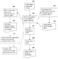
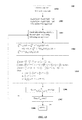
- FIG. 1 is a block diagram illustrating path based SSTA with cross-talk analysis according to the present invention
- FIG. 2 shows the flowchart of forward propagation based on breadth first traversal in SSTA according to the present invention
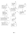
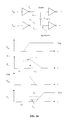
- FIG. 3 is an example circuit for illustrating the concept of forward propagation based on breadth first traversal and backward search based on depth first traversal in SSTA;
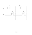
- FIG. 4 illustrates an example timing diagram for several clock phases
- FIG. 5 shows an example timing graph of forward propagation in the presence of uniform timing constraint
- FIG. 6 is the flowchart for the algorithm of forward propagation with non-uniform timing constraint
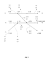
- FIG. 7 is the timing graph showing an example of criticality calculation results for the example circuit with non-uniform timing constraints
- FIG. 8 is a flowchart illustrating a method for backward propagation to generate all critical paths
- FIG. 9 is a flowchart for the algorithm of pre-characterizing cells up to the second order of variation effect.
- FIG. 10 is a flowchart for RLC solver of admittance matrix with variation effects to the second order
- FIG. 11 is a flowchart calculating the effective capacitance in the presence of variation effect to the second order with one port in RLC;
- FIG. 12 shows an example circuit with the driver's immediate output waveform in terms of t x and t D ;
- FIG. 13 is a flowchart calculating the effective capacitance in the presence of variation effect to the second order with cross-talk in RLC;
- FIG. 14 shows an example circuit illustrating the victim's and aggressor's immediate output waveforms in terms of t x and T d ;
- FIG. 15 is a flowchart for RLC solver of voltage transfer with variation effects to the second order
- FIG. 16 shows an example finding time t up to the second order of random parameter for waveform reaching certain value.
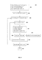
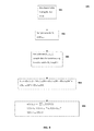
- a circuit description 101 which can be complicated in the presence of multi-phase sequential elements, is accepted by the tool SSTA 102 handling non-uniform timing constraints since paths between source and destination flip-flops can have different timing constraints.
- the circuit description 101 can be at gate level, or combination of gate and transistor level, due to the fact the tool targets at hybrid design. Since the transistor level description can be partitioned into gates, the timing analysis will be handled similarly at gate level. Our discussion for SSTA is limited to gate level, and there is no need to specifically distinguish gate and transistor level.
- the SSTA tool 102 is used to pre-characterize timing of the cells in terms of a second-order delay model instead of first-order approximation 103 and results go to a file 106 used for future runs.
- the tool 102 is also used 104 to interconnect solver generating information needed to gate level delay calculation also up to second order of process variation effect and store the results in a file 105 .
- SSTA 102 carries out timing check for all paths with non-uniform timing constraints in two steps, namely forward propagation based on BFS 107 and backward traversal using DFT 108 . However, the detailed algorithms are different from those published algorithms by Visweswariah. The final result reports the critical path in terms of the probability of the path 109 .
- new timing analysis algorithm 107 108 in this tool of SSTA with uniform or non-uniform timing constraint 102 is discussed here in detail.
- x can be a vector with each component representing independent process parameter.
- transistor width and length are two independent process parameters.
- MAX(X,Y) is used to store PDF of max of the two random variables X and Y.
- a gate has two inputs i1 and i2 and one gate output out with their latest arrival times at two inputs i1 and i2 stored as two random variables A and B, respectively.
- Two delays delay i1 ⁇ out out and delay i2 ⁇ out out are represented by C and D also as random variables.
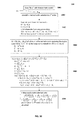
- FIG. 2 shows the flowchart of forward propagation based on BFS 107 .
- the accumulated probability (accum_prob) of the node which is the most critical probability for all paths ending at the said node, is being found in the following way.
- FIG. 3 A simple sequential circuit with 6 flip-flops is shown in FIG. 3 and the clock phases P1 and P2 are shown in FIG. 4 .
- L1-L6 are positive edge-triggered flip-flops, and all of them are controlled by the rising clock edge of clock phase P1.
- the outputs of flip-flops 11, 13, and 15 as shown in FIG. 5 are put into queue 201 and start processing queue elements if queue is not empty 202 .
- fanout gate D 203 is checked. D begin to be evaluated since two inputs have been visited 204 .
- MAX(13,15) is calculated and the latest arrival time at d in terms of a random variable is obtained 204 .
- the node name and the random variable associated with the node are expressed by the same symbol for the sake of clarity.
- 13 refers to both node and its random variable.
- the probabilities from 13 to d and from 15 to d are calculated to be 0.3 and 0.7, respectively.
- accm_prob is for 1, since they are the outputs of single input gates.
- the accum_prob are 1, 0.8, and 0.8.
- the arrival times at c, f, and g have been computed.
- the probability P for the failure of the path from 13 to f 207 .
- y can be a vector with several process parameters.
- FIG. 6 is the flowchart for the algorithm of 107 with non-uniform timing constraint. Still referring to FIG. 3 for the sequential circuit and FIG. 4 for the clock phases, here we assume that L1-L6 are positive edge-triggered flip-flops, L3 and L4 are controlled by the rising clock edge of clock phase P2, while the remaining flip-flops are controlled by the rising edge of P1. Referring to the flowchart in FIG. 6 and the timing graph as shown in FIG. 7 , signals start propagating from outputs of flip-flops 11, 13, and 15 similar to FIG. 2 201 202 and process gate when all inputs are visited 203 . The difficulty for non-uniform case can be understood by the processing of gate D in FIG. 3 .
- the inputs 13 and 15 store latest arrival times with respect to rising edge of clock phases P2 and P1 601 , respectively.
- driven clock phases are P1 and P2 602 , instead of only one clock phase either P1 or P2.
- choose any pair of clock phases from the two inputs add input delays to the latest arrival times with the two clock phases, compare with all driven clock phases 602 . If the ordering of these two clock phases is not fixed, then latest arrival times for these two clock phases must be stored in the output d of the said gate D 603 . This part in fact is similar to that used in STA addressed in detail by Chang elsewhere.
- SSTA the nominal numbers in the random variable of the latest arrival time are used to determine the clock phases with respect to which the latest arrival times at node d in terms of random variable are stored.
- the accumulated path probability with respect to each clock phase stored at the said node d is needed.
- the accum_prob at 13 with respect to clock phase p2 is 1, so is accum_prob at 15 with respect to clock phase P1.
- the aforementioned probability edge_prob(13,d,P2,P2) associated with each clock phase of the input and each clock phase at the output is stored into the clock phase of the input.
- the forward propagation process stops when all signals have reached inputs of destination flip-flops.
- the delay variables for these nodes have been obtained.
- Probability for failure at the said node can be computed from the delay variable and its timing constraint. If the probability is greater than the user specified threshold probability, the difference is slack in terms of probability, not in terms of time.
- FIG. 7 is the timing graph showing an example of criticality calculation results for the circuit in FIG. 3 with non-uniform timing constraints.
- the accum_prob at each node is expressed as a vector for each phase.
- the accum_prob are (1,0), (0,1) and (1,0), meaning at 11 the accum_prob is 1 with respect to P1, at 13 the accum_prob is 1 with respect to P2, and at 15 the accum_prob is 1 with respect to P1.
- the latest arrival times are calculated from the latest arrival times at node 13 and 15 plus the delays from 13 to node d and 15 to d, respectively.
- edge_prob [ 0.7 , 0 0 , 0 ]
- P 11 edge_prob(1,e,P1,P1). Note that the 2nd row is (0,0) because input a does not have any delay associated with P2. Since node a does not store the longest delay with respect to P2, the longest delay with respect to P2 in node d does not merge with any delay from a, meaning the probability of the delay from d with respect to phase P2 goes to node e also with respect to P2 is 1. This explains the matrix edge probability P between d and e is
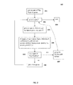
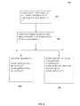
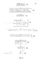
- This invention presents an algorithm 108 for backward propagation to generate all critical paths as shown in FIG. 8 .
- First identify the data input of the flip-flops with negative slack, meaning the paths ending at the said node with path probability exceeding the specified threshold probability. It is noted that the accumulated probability at the said node times A in which A user specified probability-slack is the probability of failure cur_prob for the most critical path ending at the said node 801 .
- Search paths backward recursively based on DFT from these said nodes with arguments for node f, its clock phase P, and to only generate failing paths with their probabilities greater than the user specified threshold 802 .
- the procedure of back trace DFT in the presence of multi-phase circuit goes as follows.
- the purpose is to determine if there are paths coming from the said input e to the said node f exceeding the user specified threshold probability.
- the said nodes e and f store the nominal and variation terms of latest arrival times for various independent clock phases and we choose one clock phase of e, say Q 804 , for illustration purpose.
- x edge_prob( e,f,Q,P )
- y accum_prob( e,Q )
- z accum_prob( f,P )
- this said critical path failure probability at node f is obtained by integrating the delay time in terms of random variable at node f with respect to the whole variation space by considering timing constraint.
- the purpose is to trace back from node f to find the three critical paths in FIG. 7 , namely paths consisting of nodes 11 ⁇ a ⁇ e ⁇ f, 13 ⁇ d ⁇ e ⁇ f, and 15 ⁇ d ⁇ e ⁇ f.
- Pre-characterizing cell generates the mathematical equations describing the cell delay and output slew as a function of cell input slew time and cell output loading, with loading and delays being treated as random variables 901 .
- These random variables have non-Gaussian PDF and they are expressed by the random variables with normalized Gaussian PDF due to the independent process parameters such as transistor width and transistor length etc. to the second order.
- D in ⁇ out The delay of the cell from cell input to cell output denoted by D in ⁇ out is discussed similarly, and there is no need to repeat it here.
- the SSTA engine is further complicated by the variation effects due to the RLC interconnect by referring to 104 in FIG. 1 .
- effective capacitance approach is used in the case of the gate driving the interconnect delay and the cross-talk problems using both the well-known admittance matrix and voltage transfer which are expressed in terms of pole and residue format as a function of variation parameters by referring to the file 105 FIG. 1 .
- This invention presents an algorithm of 104 for RLC solver as shown in FIG. 10 . First, the algorithm checks whether the file containing admittance matrix and voltage transfer already exists 1001 . If so, then skip the procedures of re-computing admittance matrix and voltage transfer and directly read information from the said file.
- x p are the m port node voltages and x i include n internal node voltages and l inductor currents.
- G P is m ⁇ m matrix for m ports, so is C P .
- G I and C I are (l+n) ⁇ (l+n) matrices representing n internal nodes and l inductors.
- Both G C and C C are (l+n) ⁇ m connection conductance and susceptance matrices, respectively.
- the right hand side is a (m+l+n) ⁇ m matrix with b P as being the external current at the m port nodes.
- Y ( s ) G P +sC P ⁇ ( G C +sC C ) T ( G I +sC I ) ⁇ 1 ( G C +sC C ) Kerns and Yang have pointed out that by using Cholesky factorization G I can be transformed into unit matrix. Since this part will not affect the later discussions, it is omitted for the sake of brevity.
- R 0 and C 0 are nominal values and a and b are two independent variation parameters for resistance and capacitance, respectively 1003 .
- V i stands for ith random variable up to the second order.
- V i can be one of random variables a, b, ab, a 2 , and b 2 in which a and b are independent process parameter with normalized Gaussian distribution N(0,1).
- the nominal value of G I is G I0 and G Ii is the coefficient matrix of random variable y i .
- the matrices C P , G P , C P , G C and C C are all defined similarly. To simplify the calculation the congruence transform is carried out by using
- G I,0 ⁇ 1 G I,0 ⁇ 1 ⁇ G I,0 ⁇ 1 VG I,0 ⁇ 1 +G I,0 ⁇ 1 VG I,0 ⁇ 1 V
- G I0 ⁇ 1 Note that the square terms for the random variables in V doesn't contribute in V 2 since we only need up to the 2nd order term of random variable.
- X 0 is the nominal part of X
- V is the variation part consisting N variational terms up to the second order of each independent variation parameter
- X i is the coefficient of each variation term v i .
- the next step is to use Arnoldi's procedure in finding the orthonormal bases [W 0 ,W 1 , . . . W q ⁇ 1 ] for the Krylov space Kr(G I ⁇ 1 C I , G I ⁇ 1 G C , q) for matching q moments of the multiport admittance.
- W I which is G I ⁇ 1 G C
- QR decomposition if the circuit has more than one port.
- W i0 is the nominal part of ith vector W i
- W i,m is the coefficient of the mth random parameter v m which may contain second order of independent random variable.
- Set W [W 0 W 1 . . . W q ⁇ 1 ] which is an orthonormal matrix spanning the Krylov space Kr(G I ⁇ 1 C I , G I ⁇ 1 G C , q).
- Y(s) G P +sC P ⁇ ( ⁇ tilde over (G) ⁇ C ) T ( I+s ⁇ tilde over (G) ⁇ I ⁇ 1 ⁇ tilde over (C) ⁇ I ) ⁇ 1 ( ⁇ tilde over (G) ⁇ I ⁇ 1 ⁇ tilde over (G) ⁇ C )
- the variation parts V, Y, and Z contain second order terms, so the quadratic terms like sV sV only contain 2nd order terms. Since A 0 is the reduced matrix without variation, this matrix can be diagonalized by using congruence transform U consisting of eigenvectors of A 0 . For the sake of brevity of notation, A 0 is diagonalized matrix containing the eigenvalues of the original A 0 . The matrix V after the congruence transform U cannot be diagonalized.
- the method in calculating the effective capacitance in the presence of variation effect is further discussed in FIG. 11 with one port 1101 after we have obtained the admittance matrix in terms of poles and residues expressed in powers of variation parameters read from file 105 .
- the well-known criterion is used in obtaining effective capacitance, namely requiring the charge injected into the driving node of RLC interconnect from the driving gate using effective capacitance to be the same as that as obtained by using voltage at the said driving node and the admittance matrix for the RLC.
- this method by using an example for the voltage wave form at the driving node of RLC, although the method is readily apparent to those of ordinary skill in the art for different types of voltage waveform.
- V ⁇ ( t ) ⁇ V i - ct 2 0 ⁇ t ⁇ t x a + b ⁇ ( t - t x ) t x ⁇ t ⁇ t D ⁇ f ⁇ ⁇ e td + V f t ⁇ t D
- V i is the initial value Vdd (0) when V(t) is in fall(rise) transition
- V f is the final node value Vdd (0) when V(t) is in rise(fall) transition.
- t 0 is 0.
- t x to be the time when the voltage falls(rises) to 80%(20%) of Vdd.
- the admittance is written as follows assuming there is one port 1102 .
- C eff is achieved by using the above formula iteratively.
- the initial choice of C eff can be chosen to be the total routing capacitance 1103 .
- the above formula is evaluated as follows. To make notation simple, ⁇ and ⁇ are used in replacement of ⁇ k and ⁇ k without loss of generality. We have
- the constant ⁇ then is independent of the summation of each pair of pole and residue. All the constants have variation terms to the second order.
- the coefficients b and c, and delays t D and t x are also random variables calculated by using pre-characterized timing library with variations from input slew time and output loading based on C eff during the process of iteration until the final C eff is obtained. Therefore, with all of terms such as poles, residues, t x and t D being calculated to the 2nd order of random parameters, the term Q(t) up to the 2nd order of random parameters can also be achieved.
- the method in calculating the effective capacitance in the presence of variation effect is further discussed in FIG. 13 with cross-talk 1301 after we have obtained the admittance matrix in terms of poles and residues expressed in powers of variation parameters read from file 105 . Without loss of generality, assuming there are two ports for one victim and one aggressor as shown in FIG. 14 .
- C eff , 1 Q 1 b 1 ⁇ ( t D , 1 - t x , 1 / 2 ) C eff,2 is obtained similarly.
- C eff,1 and C eff,2 are also calculated to the 2nd power in random parameters.
- the process is iterated until convergence 1307 is reached.
- the discussion on victim glitch is exactly the same as that in the case of calculating maximum delay of the victim except setting voltage a constant at the input of the victim driver. Therefore, there is no further discussion on glitch in cross-talk.
- V out ( s ) T ( s ) V in ( s ) in which Vout (s) is a m ⁇ 1 matrix, T(s) is m ⁇ n matrix and Vin (s) is n ⁇ 1 matrix with each matrix element being a random variable up to the 2 nd order of variation effects. Both admittance matrix and voltage transfer are treated under the same formulation.
- the matrix element of T(s) does not include ⁇ + ⁇ s. Similar to the handling of admittance matrix the voltage transfer can be expanded to the 2 nd order of variation terms, and then fitted into simple pole and residue including variation terms to obtain poles and residues to the second order of variations.
- V out (s) is a 3 ⁇ 1 matrix
- T(s) is 3 ⁇ 2 matrix
- V in (s) is 2 ⁇ 1 matrix
- V out,1 (t) and V out,2 (t) refer to waveform at output nodes of victim and aggressor, respectively.
- V out,1 ( t ) ⁇ 1 ( T 11 ( s ) V in,1 ( s ))+ ⁇ 1 ( T 12 ( s ) V in,2 ( s ))
- V in,1 (t) and V in,2 (t) are defined similarly as in the discussion of effective capacitance for the case of one port with the combination of three regions including quadratic, linear and exponential forms. In the actual implementation the quadratic part can be neglected without suffering too much inaccuracy.
- V in,1 (t) stays at initial constant value V i , which is either Vdd or 0 depending on fall or rise transition at RLC input, for the period of time denoted by t 0 before the waveform starts changing.
- V in,1 (t) and V in,2 (t) have their own t 0 , meaning they have different switching times.
- V in,1 ( t ) a+b ( t ⁇ t x )
- the starting point t 0 when V in,1 (t) changes from initial value V i is
- the function f(t, ⁇ ) is further expanded in power of ⁇ t 1603
- This invention solves the problem by adopting Non-Gaussian behavior and provides a method to pre-characterize the timing library for the gate output delay and slope as random variables as a function input slope and output loading up to the 2 nd order of variation.
- This invention provides a novel way to calculate admittance matrix and voltage transfer up to 2 nd order of process variation and fitted the results into simple pole format to obtain poles and residues for each matrix element up to 2 nd order of variation. Effective capacitance and interconnect delay can be calculated up to 2 nd order of variation by using poles and residues including up to second order variation effects of both admittance matrix and voltage transfer, accordingly.
- the invention further provides a method for cross-talk with multiple ports to evaluate effective capacitances at the ports individually and waveforms at the ports are then used to calculate delay expressed as random variable containing 2 nd order variation terms at victim outputs. With all of these in place, SSTA is used to identify critical paths in terms of probability in an accurate manner.
- timing verification tool may have one or more of the above-described capabilities in any combination, and any of these novel capabilities can be combined with conventional or other novel timing verification tools.
Landscapes
- Engineering & Computer Science (AREA)
- Computer Hardware Design (AREA)
- Physics & Mathematics (AREA)
- Theoretical Computer Science (AREA)
- Evolutionary Computation (AREA)
- Geometry (AREA)
- General Engineering & Computer Science (AREA)
- General Physics & Mathematics (AREA)
- Design And Manufacture Of Integrated Circuits (AREA)
Abstract
Description
A=a+bx
in which x is a random variable with normalized Gaussian distribution N(0,1). The PDF fx for random variable x is
f x(x)=1/√2πexp(−x 2)
f x(x)=1/√2πexp(−((x−a)/b)2)
A=a+bx+cx 2
Note that x can be a vector with each component representing independent process parameter. For example, transistor width and length are two independent process parameters.
In SSTA the operation MAX(X,Y) is used to store PDF of max of the two random variables X and Y. Suppose a gate has two inputs i1 and i2 and one gate output out with their latest arrival times at two inputs i1 and i2 stored as two random variables A and B, respectively. Two delays delayi1→out out and delayi2→out out are represented by C and D also as random variables. The latest arrival times in terms of random variables at out from the two inputs i1 and i2 are E and F, respectively. We have
A=a 0 +a 1 ×+a 2 x 2
B=b 0 +b 1 ×+b 2 x 2
C=c 0 +c 1 x+c 2 x 2
D=d 0 +d 1 x+d 2 x 2
E=(a 0 +c 0)+(a 1 +c 1)x+(a 2 +c 2)x 2
F=(b 0 +d 0)+(b 1 +d 1)x+(b 2 +d 2)x 2
MAX(E,F)=e 0 +e 1 x+e 2 x 2
Then, MAX(E,F) is computed to get e0, e1 and e2 and it is the latest arrival time in terms of a random variable stored at the output of the gate. The computation of e0, e1 and e2 by Zhan et al. is already quite well-known, and there is no need to repeat them here. In SSTA the probability of the path is needed besides the latest arrival time which is random variable. Still using the above example of a gate with two inputs, we need to know the probability for each of the two paths, namely from i1 to out and i2 to out. This information is obtained from the calculation of MAX(E>F) and MAX(F>E) with MAX(E,F)=MAX(E>F)+MAX(F>E). The probability for E>F is obtained by integrating the PDF (Probability Density Function) of MAX(E>F) and same for F>E.
P=
Here y can be a vector with several process parameters.
P=
edge_prob(e,f,P1,P1)=Prob(d1>d2)
in which e and f refer to input and output node, and the 3rd argument is the clock phase the delay at input is associated with, and the 4th argument is the clock phase the delay at output is associated with. Then, edge_prob(e,f,P2,P1)=Prob(d2>d1) follows similarly.
As accum_prob at node f, since d3 is measured from phase P1, and there are two paths from e to f with two different clock phases. The
accum_prob(f,P1)=max(accum_prob(e,P1)*Prob(d1>d2), accum_prob(e,P2)*Prob(d2>d1))
Similar to the case of uniform timing constraint, the forward propagation of the signals stop when the signals have reached inputs of destination flip-flops and the probability for failure at the said nodes are calculated 207.
Using the previous notation for edge_prob, we have P11=edge_prob(1,e,P1,P1).
Note that the 2nd row is (0,0) because input a does not have any delay associated with P2. Since node a does not store the longest delay with respect to P2, the longest delay with respect to P2 in node d does not merge with any delay from a, meaning the probability of the delay from d with respect to phase P2 goes to node e also with respect to P2 is 1. This explains the matrix edge probability P between d and e is
With the information of accum_prob at nodes a and d, and the edge matrix probabilities between edges a to e and d to e, the accum_prob at node e is obtained easily.
accum_prob(e,P1)=max(accum_prob(a,P1)*edge_prob(a,e,P1,P1),
accum_prob(d,P1)*edge_prob(d,e,P1,P1))=max(1*0.7,1*0.3)=0.7
accum_prob(e,P2)=1
This is how we get 0.7,1 for node e in
and edge_prob(e,f,P2,P1)=0.1. In terms of edge matrix it is
accum_prob(f,P1)=max(accum_prob(e,P1)*edge_prob(e,f,P1,P1),
accum_prob(e,P2)*edge_prob(e,f,P2,P1))=max(0.7*0.9,1*0.1)=0.63
accum_prob(f,P1)=0.63
accum_prob(f,P2)=0
In
x=edge_prob(e,f,Q,P)
y=accum_prob(e,Q)
z=accum_prob(f,P)
new_prob=cur_prob*y*x/z
By comparing new_prob with user specified threshold probability, it can be determined whether the path search can go beyond this node e. If so, then the process is done recursively 807. If not then the next clock phase Q of node e will be accessed and the same process continues 808. Then, when the clock phases of node e are exhausted, the next input of gate F is accessed 809 and so on until all critical paths with probability greater than user specified threshold probability.
X=a+bx+cy+dx 2 +ey e +fxy
in which x and y refer to random variables for transistor width and transistor length, respectively assumed to have normalized Gaussian distribution N(0,1). If X is for cell output slew time, then the coefficients a, b, c etc. depend on the cell input slew time and output loading which are also random variables. With this understanding, the procedure of pre-characterizing cell in the presence of variation effect is described as follows. The purpose is to characterize, say output slew S as a function of input slew, output loading and transistor width, length into
S out =a(S in ,L out)+b(S in ,L out)W+c(S in ,L out)W+d(S in ,L out)W 2 +e(S in ,L out)W 2 +f(S in ,L out)WL
The delay of the cell from cell input to cell output denoted by Din→out is discussed similarly, and there is no need to repeat it here. Since we use N(1,0) for x any y representing random variables for width W and length L, in the modeling W in fact is (W−μ)/σ assuming N(μ,σ) is the Gaussian PDF for W, and L follows the same. In the sampling for Sin and
a(S in ,L out)=ƒ(i)Y(i)
Y(1)=S in Y(2)=L out *S in Y(3)=(L out)3
Y(4)=L out Y(5)=1
S out =A+Bx+x t Cx
where x=(x1,x2, . . . xn)t is 1×n vector representing n independent process parameters with normalized Gaussian PDF N(1,0), B is 1×n vector, and C is a n×n symmetric matrix and A is a scalar, which is the constant term. We have
A=Σ i=1 5 a(i)Y(i)
B m=Σi=1 5 b(m,i)Y(i)
C mn=Σi=1 5 c(m,n,i)Y(i)
in which Bm is the mth component of vector B, while Cmn is element of matrix C at row m and column n.
(G+sC)x=b
In MNA there are two types of elements,
Assuming there are m ports and n internal nodes in RLC circuit, here xp are the m port node voltages and xi include n internal node voltages and l inductor currents. GP is m×m matrix for m ports, so is CP. GI and CI are (l+n)×(l+n) matrices representing n internal nodes and l inductors. Both GC and CC are (l+n)×m connection conductance and susceptance matrices, respectively. The right hand side is a (m+l+n)×m matrix with bP as being the external current at the m port nodes. The admittance Y(s) is defined as
Y(s)x P(s)=b P(s)
Through some calculation by eliminating xi, by following Kerns formulation without considering variations Y(s) is obtained as follows,
Y(s)=G P +sC P−(G C +sC C)T(G I +sC I)−1(G C +sC C)
Kerns and Yang have pointed out that by using Cholesky factorization GI can be transformed into unit matrix. Since this part will not affect the later discussions, it is omitted for the sake of brevity.
R=R 0 +R 1 a
Similarly capacitance C has Gaussian distribution like
C=C 0 +C 1 b
Here R0 and C0 are nominal values and a and b are two independent variation parameters for resistance and capacitance, respectively 1003. By using these, it is straightforward to evaluate G and C matrices in powers of a and b. We have
G I =G I,0 +V
V=Σ i=1 N G Ii V i
Here Vi stands for ith random variable up to the second order. For example if there are two random parameters a and b, then Vi can be one of random variables a, b, ab, a2, and b2 in which a and b are independent process parameter with normalized Gaussian distribution N(0,1). The nominal value of GI is GI0 and GIi is the coefficient matrix of random variable yi. The matrices CP, GP, CP, GC and CC are all defined similarly. To simplify the calculation the congruence transform is carried out by using
After the congruence transform XTGX and XTCX the connection susceptibility matrix CC becomes zero and Y(s) still remains the same. It is noted that the above mentioned X has V dependency. In the calculation we need to preserve up to V2 term since V contains 1st order of random variable and we need computation to the 2nd order. For example,
G I −1=(G I,0 +V)−1=(I+G I,0 −1 V)−1 G I,0 −1 =G I,0 −1 −G I,0 −1 VG I,0 −1 +G I,0 −1 VG I,0 −1 V G I0 −1
Note that the square terms for the random variables in V doesn't contribute in V2 since we only need up to the 2nd order term of random variable. Therefore, X can be calculated to be
X=X 0 +V
V=Σ i=1 N X i v i
Where X0 is the nominal part of X, V is the variation part consisting N variational terms up to the second order of each independent variation parameter and Xi is the coefficient of each variation term vi.
For the sake of brevity of notation we stick to the same formula for Y(s) after congruence transform by X with the understanding that Cc is zero and the remaining matrices still up to the 2nd order of random variables but with different matrix coefficients. The admittance matrix Y(s) can then be written as
Y(s)=G P +sC P−(G C)T(I+sG I −1 C I)−1(G I −1 G C)
The next step is to use Arnoldi's procedure in finding the orthonormal bases [W0,W1, . . . Wq−1] for the Krylov space Kr(GI −1 CI, GI −1 GC, q) for matching q moments of the multiport admittance. We start with WI, which is GI −1 GC and followed by QR decomposition if the circuit has more than one port. It is worth noting that in QR process, we need to get vector divided by its norm. Here we use a simple example to illustrate this concept. Assuming there is one random parameter x, a vector with two components up to the second order of x is something like
The norm is obtained by first taking the square
(4+2x+3x 2)2+(3+1x+2x 2)2=(16+16x+28x 2)+(9+6x+13x 2)=25+22x+41x 2
Then square root is in the format of (a+bx+cx2), and we easily get 5+2.2x+7.232x2. As to W2, W3 etc. they are obtained through standard procedure of Gram-Schmidt orthogonalization. We end up with the Arnoldi vector Wi (i=0, 1 . . . q−1) with variation effect as follows
W i =W i0 +M
M=Σ m=1 N W i,m v m
{tilde over (G)} I =W T G I W
{tilde over (C)} I =W T C I W
{tilde over (G)} C =W T G C
Y(s)=G P +sC P−({tilde over (G)} C)T({tilde over (G)} I +s{tilde over (C)} I)−1({tilde over (G)} C)
Y(s)=G P +sC P−({tilde over (G)} C)T(I+s{tilde over (G)} I −1 {tilde over (C)} I)−1({tilde over (G)} I −1 {tilde over (G)} C)
A={tilde over (G)} I −1 {tilde over (C)} I =A 0 +V
V=Σ i=1 N V i y i
B={tilde over (G)} I −1 {tilde over (G)} C =B 0 +Y
Y=Σ i=1 N Y i y i
C=({tilde over (G)} C)T =C 0 +Z
Z=Σ i−1 N Z i y i
Note that A is the reduced matrix by Arnoldi method by considering variation effects up to the 2nd order of random parameters. Here we have 1005
calculated to the 2nd order of random parameters. The variation parts V, Y, and Z contain second order terms, so the quadratic terms like sV sV only contain 2nd order terms. Since A0 is the reduced matrix without variation, this matrix can be diagonalized by using congruence transform U consisting of eigenvectors of A0. For the sake of brevity of notation, A0 is diagonalized matrix containing the eigenvalues of the original A0. The matrix V after the congruence transform U cannot be diagonalized. The right hand matrices B0=UT B0, Y=UT Y and the left hand matrices C0=UC0, Z=UZ. By simple observation for each matrix element of Y(s) it can have the form of simple, double, and cubic pole etc. However, we need to express simple pole and residue with its variation terms. Here we adopt the method by expanding pole and residue form in powers of variation parameters and compare with the exact solution of Y(s) to obtain the coefficients of variation terms for pole and residue. The procedure can be illustrated by the following example. Assuming there is only one random parameter x with the pole and residue form can be shown as follows 1006
The purpose is to find coefficients for random parameter x for the pole −α and residue β. By comparing with the exact result from Y(s) in powers of x and 1/(s+α) we can obtain a and c from x term and b and d from x2 term. Note that in this example 1/(s+α)3 term for x2 term in fact is not needed, since the unknown a in the coefficient a2β has already been obtained in the other terms.
As shown in
in which Vi is he initial node value of the interconnect, and i(s) is the Laplace transform of the current i(t) at the said driving node of RLC interconnect. We require that
Here
Making use of
We obtain 1105
Note that in the above formulae, the pole γ and residue δ refer to one of the poles and residues, and the summation with respect to all poles and residues are implied. The constant α then is independent of the summation of each pair of pole and residue. All the constants have variation terms to the second order. The coefficients b and c, and delays tD and tx are also random variables calculated by using pre-characterized timing library with variations from input slew time and output loading based on Ceff during the process of iteration until the final Ceff is obtained. Therefore, with all of terms such as poles, residues, tx and tD being calculated to the 2nd order of random parameters, the term Q(t) up to the 2nd order of random parameters can also be achieved. For example, in calculating Q(t=tD), we have one term like eγ t D with γ=γnom+X and tD=tD,nom+Y in which X and Y include variation terms up to 2nd order. Then, eγt(t=tD)=eγ nomtD,nom (1+XtD,nom+Yγnom+XY tD,nomγnom+X2 tD,nom 2+Y2γnom 2+2 XYtD,nomγnom). By combining the coefficients of the same random parameter with the same order, eγt(t=tD) becomes eγ nom t D,nom Z where Z contain variation terms up to 2nd order. The calculation is straightforward but very tedious, so the final formula up to the 2nd order is not given here. Eventually we obtain Q(t=tD)=Q0+W with W being the variation term up to 2nd order of variation effects. Using 1106
Ceff is reevaluated 1107, and using new Ceff, which is a random variable up to 2nd order of random parameter, to obtain new constants such as tD, tx, a, b, c and achieve new Q(t) accordingly. This process is iterated until
A 11(s)V 1(s)+A 12(s)V 2(s)=i 1(s)
A 21(s)V 1(s)+A 22(s)V 2(s)=i 2(s)
in which A11 is the matrix element of 2×2 admittance matrix, V1(s)(i1(s)) and V2(s) (i2(s)) are voltages(currents) in s domain at victim and aggressor node. The purpose is to iteratively 1303 find the effective capacitances Ceff,1 and Ceff,2 at victim and
∫0 t
=Q 11 +Q 12=∫0 t
Note that waveforms V1(t) and V2(t) in time domain at
Ceff,2 is obtained similarly. Through tedious calculation all of the above constants are random variable with nominal part and variation part up to the 2nd order of random parameter, thus Ceff,1 and Ceff,2 are also calculated to the 2nd power in random parameters. The process is iterated until
V out(s)=T(s)V in(s)
in which Vout (s) is a m×1 matrix, T(s) is m×n matrix and Vin (s) is n×1 matrix with each matrix element being a random variable up to the 2nd order of variation effects. Both admittance matrix and voltage transfer are treated under the same formulation. By using the same Arnoldi's
Ñ=W T N
T(s)=−({tilde over (N)})T(I+s{tilde over (G)} I −1 {tilde over (C)} I)−1({tilde over (G)} I −1 {tilde over (G)} C)
here N being defined as n×m matrix if the circuit has n outputs and m internal nodes and N initially prior to congruence transform by W, assuming CC is zero without loss of generality, is
N ij=1 if i th input=j th internal node
By comparing T(s) with Y(s)
Y(s)=G P +sC P−({tilde over (G)} C)T(I+s{tilde over (G)} I −1 {tilde over (C)} I)−1({tilde over (G)} I −1 {tilde over (G)}C)
as obtained before, we see that GP+s CP is not contained in T(s) and {tilde over (G)}C in Y(s) is replaced by Ñ in T(s). Thus, the matrix element of T(s) does not include α+βs. Similar to the handling of admittance matrix the voltage transfer can be expanded to the 2nd order of variation terms, and then fitted into simple pole and residue including variation terms to obtain poles and residues to the second order of variations. Without loss of generality we assume Vout (s) is a 3×1 matrix, T(s) is 3×2 matrix and Vin (s) is 2×1 matrix, Vout,1(t) and Vout,2(t) refer to waveform at output nodes of victim and aggressor, respectively. For
V out,1(t)=
Vin,1 (t) and Vin,2 (t) are defined similarly as in the discussion of effective capacitance for the case of one port with the combination of three regions including quadratic, linear and exponential forms. In the actual implementation the quadratic part can be neglected without suffering too much inaccuracy. In this approximation Vin,1 (t) stays at initial constant value Vi, which is either Vdd or 0 depending on fall or rise transition at RLC input, for the period of time denoted by t0 before the waveform starts changing. Vin,1 (t) and Vin,2 (t) have their own t0, meaning they have different switching times. Using the aforementioned formula as follows,
V in,1(t)=a+b(t−t x)
The starting point t0 when Vin,1 (t) changes from initial value Vi is
The waveform at the RLC input is as follows 1504,
It is emphasized that all of t, t0 and tD are measured from the origin which is the starting point when the input of the driver starts changing. We have
The notation for summing all pairs of residue and pole is omitted. In actual calculation it is neat to change t coordinate from to and tD becomes tD−t0, and then replace t by t−t0. We have 1505
After the waveform at the output node of the victim is obtained, the next step is to find the time tout,1 at which the waveform of the victim Vout,1(t) is at 50% of Vdd, then the delay from the input of RLC input, say
Delay=t out,1 −t D,1
Note that Delay is a random variable up to the 2nd order variation effect. Knowing that all the constants such as t0, tD, f, d, b in fact are random variables expressed by random parameters up to the second order, the waveform at output node is also a random variable up to the 2nd order effect. We use an example as shown in
f(t,α)=f 0(t)+f 1(t)α+f 2(t)α2
The purpose is to find the random variable t being expressed as 1602
t=t n +Δt=t n +xα+yα 2
f(t,α)=0.5 Vdd
The function f(t,α) is further expanded in power of
We therefore obtain tn, x and y as by solving the following equations sequentially 1604
Claims (13)
accum_prob(c,P2)=max(accum_prob(e,P1)*edge_prob(e,c,P1,P2),accum_prob(f,P2)*edge_prob(f,c,P2,P2)).
x=edge_prob(e,f,Q,P)
y=accum_prob(e,Q)
z=accum_prob(f,P);
new_prob=cur_prob*y*x/z;
R=A+Bx+x t Cx
a(S in ,L out)=Σi=1 5ƒ(i)Y(i)
Y(1)=S in Y(2)=L out *S in Y(3)=(L out)3
Y(4)=L out Y(5)=1.
Y(s)x p(s)=b p(S)
Y(s)=G P +sC P−(G C +sC C)T(G I +sC I)−1(G C +sC C)
G I =G I,0 +V
V=Σ i=1 N G Ii v i
W i =W i0 +V
V=Σ m=1 N W in v m
{tilde over (G)} I =W T G I W
{tilde over (C)} I =W T C I W
{tilde over (G)} C =W T G
Y(s)=G P +sC P−({tilde over (G)} C)T(I+s{tilde over (G)} I −1 {tilde over (C)} I)−1({tilde over (G)} I −1 {tilde over (G)} C)
A={tilde over (G)} I −1 C I =A 0 +V
V=Σ i=1 N V i y i
B={tilde over (G)} I −1 {tilde over (G)} C =B 0 +Y
Y=Σ i=1 N Y i y i
C=({tilde over (G)} C)T =C O +Z
Z=Σ i=1 N Z i y i;
A 11(s)V 1(s)+A 12(s)V 2(s)=i 1(s)
A 21(s)V 1(s)+A 22(s)V 2(s)=i 2(s)
V out(s)=T(s)V in(s)
Ñ=W T N
T(s)=−({tilde over (N)})T(I+s{tilde over (G)} I −1 {tilde over (C)} I)−1({tilde over (G)} I −1 {tilde over (G)} C)
N(i,j)=1 if i th input=j th internal node;
V out,1(t)=
Delay=t out,1 −t D,1.
f(t,α)=f 0(t)+f 1(t)α+f 2(t)α2
t=t n +Δt=t n +xα+yα 2
f(t,α)=0.5 Vdd;
Priority Applications (1)
| Application Number | Priority Date | Filing Date | Title |
|---|---|---|---|
| US14/591,852 US9898564B2 (en) | 2014-01-15 | 2015-01-07 | SSTA with non-gaussian variation to second order for multi-phase sequential circuit with interconnect effect |
Applications Claiming Priority (2)
| Application Number | Priority Date | Filing Date | Title |
|---|---|---|---|
| US201461927740P | 2014-01-15 | 2014-01-15 | |
| US14/591,852 US9898564B2 (en) | 2014-01-15 | 2015-01-07 | SSTA with non-gaussian variation to second order for multi-phase sequential circuit with interconnect effect |
Publications (2)
| Publication Number | Publication Date |
|---|---|
| US20150199462A1 US20150199462A1 (en) | 2015-07-16 |
| US9898564B2 true US9898564B2 (en) | 2018-02-20 |
Family
ID=53521601
Family Applications (1)
| Application Number | Title | Priority Date | Filing Date |
|---|---|---|---|
| US14/591,852 Active 2035-05-12 US9898564B2 (en) | 2014-01-15 | 2015-01-07 | SSTA with non-gaussian variation to second order for multi-phase sequential circuit with interconnect effect |
Country Status (1)
| Country | Link |
|---|---|
| US (1) | US9898564B2 (en) |
Cited By (2)
| Publication number | Priority date | Publication date | Assignee | Title |
|---|---|---|---|---|
| US20180359851A1 (en) * | 2017-06-07 | 2018-12-13 | International Business Machines Corporation | Modifying a Circuit Design |
| US10275554B1 (en) * | 2017-07-17 | 2019-04-30 | Cadence Design Systems, Inc. | Delay propagation for multiple logic cells using correlation and coskewness of delays and slew rates in an integrated circuit design |
Families Citing this family (4)
| Publication number | Priority date | Publication date | Assignee | Title |
|---|---|---|---|---|
| US9847125B2 (en) * | 2015-08-05 | 2017-12-19 | University Of Rochester | Resistive memory accelerator |
| US10387595B1 (en) * | 2017-05-09 | 2019-08-20 | Cadence Design Systems, Inc. | Systems and methods for modeling integrated clock gates activity for transient vectorless power analysis of an integrated circuit |
| US11556145B2 (en) * | 2020-03-04 | 2023-01-17 | Birad—Research & Development Company Ltd. | Skew-balancing algorithm for digital circuitry |
| CN112085092B (en) * | 2020-09-08 | 2023-06-20 | 哈尔滨工业大学(深圳) | Graph matching method and device based on space-time continuity constraint |
Citations (7)
| Publication number | Priority date | Publication date | Assignee | Title |
|---|---|---|---|---|
| US5680332A (en) * | 1995-10-30 | 1997-10-21 | Motorola, Inc. | Measurement of digital circuit simulation test coverage utilizing BDDs and state bins |
| US20040044510A1 (en) * | 2002-08-27 | 2004-03-04 | Zolotov Vladamir P | Fast simulaton of circuitry having soi transistors |
| US7086023B2 (en) | 2003-09-19 | 2006-08-01 | International Business Machines Corporation | System and method for probabilistic criticality prediction of digital circuits |
| US20070277134A1 (en) * | 2006-05-25 | 2007-11-29 | Lizheng Zhang | Efficient statistical timing analysis of circuits |
| US7890915B2 (en) | 2005-03-18 | 2011-02-15 | Mustafa Celik | Statistical delay and noise calculation considering cell and interconnect variations |
| US7900175B2 (en) | 2005-02-03 | 2011-03-01 | Sage Software, Inc. | Method for verifying timing of a multi-phase, multi-frequency and multi-cycle circuit |
| US8244491B1 (en) | 2008-12-23 | 2012-08-14 | Cadence Design Systems, Inc. | Statistical static timing analysis of signal with crosstalk induced delay change in integrated circuit |
-
2015
- 2015-01-07 US US14/591,852 patent/US9898564B2/en active Active
Patent Citations (7)
| Publication number | Priority date | Publication date | Assignee | Title |
|---|---|---|---|---|
| US5680332A (en) * | 1995-10-30 | 1997-10-21 | Motorola, Inc. | Measurement of digital circuit simulation test coverage utilizing BDDs and state bins |
| US20040044510A1 (en) * | 2002-08-27 | 2004-03-04 | Zolotov Vladamir P | Fast simulaton of circuitry having soi transistors |
| US7086023B2 (en) | 2003-09-19 | 2006-08-01 | International Business Machines Corporation | System and method for probabilistic criticality prediction of digital circuits |
| US7900175B2 (en) | 2005-02-03 | 2011-03-01 | Sage Software, Inc. | Method for verifying timing of a multi-phase, multi-frequency and multi-cycle circuit |
| US7890915B2 (en) | 2005-03-18 | 2011-02-15 | Mustafa Celik | Statistical delay and noise calculation considering cell and interconnect variations |
| US20070277134A1 (en) * | 2006-05-25 | 2007-11-29 | Lizheng Zhang | Efficient statistical timing analysis of circuits |
| US8244491B1 (en) | 2008-12-23 | 2012-08-14 | Cadence Design Systems, Inc. | Statistical static timing analysis of signal with crosstalk induced delay change in integrated circuit |
Non-Patent Citations (13)
| Title |
|---|
| Agarwal et al., Circuit optimization using statistical static timing analysis, Conference Paper, DOI: 10.1109/DAC.2005.193825 Source: IEEE Xplore, Jul. 2005. * |
| Altan Odabasiouglu, Mustafa Celik, PRIMA: Pssive Reduced-Order Interconnect Macromodeling Algorithm, IEEE Transactions on Computer-Aided Design of Integrated Circuits and Systems, vol. 17, No. 8,pp. 645-654 Aug. 1998. |
| Anirudh Devgan, Chandramouli Kashyap, Block-based Static Timing Analysis With Uncertainty, Proc. ICCAD 2003, pp. 607-614. |
| C. Visweswariah, K. Ravindran, k. kalafala, S.G. Walker, S. Narayan First-Order Incremental Block-Based Statistical Timing Analysis, Proc. DAC 2004, pp. 331-336. |
| Chang et al., Statistical timing analysis under spatial correlations, IEEE Transactions on Computer-Aided Design of Integrated Circuits and Systems (vol. 24, Issue: 9, Sep. 2005). * |
| Jessica Qian, Satyamurthy Pullela, and Lawrence Pillage, Modeling the "Effective Capacitance" for the RC Interconnect of CMOS Gates, IEEE Transactions on Computer-Aided Design of Integrated Circuits and Systems, vol. 13, No. 12,pp. 1526-1535 Dec. 1994. |
| Kevin J. Kerns and Andrew T. Yang, Preservation of Passivity During RLC Network Reduction via Split Congruence Transformations, Stable and Efficient Reduction of Large, Multiport RC Networks by Pole Analysis via Congruence Transformations, Proc. DAC 1997, pp. 34-39. |
| Kevin J. Kerns and Andrew T. Yang, Stable and Efficient Reduction of Large, Multiport RC Networks by Pole Analysis via Congruence Transformations, Proc. DAC 1996, pp. 280-285. |
| Lizheng Zhang, Jun Shao, Charlie Chungping Chen Non-Gaussian Statistical Parameter Modeling for SSTA with Confidence Interval Analysis ISPD 2006, Apr. 9-12, 2006, pp. 33-38. |
| Sani R. Nassif, Modeling and Analysis of Manufacturing Variations, Proc. CICC 2001, pp. 223-228. |
| Soroush Abbaspour, Hanif Fatemi, Massoud Pedram, Parameterized Block-Based Non-Gaussian Statistical Gate Timing Analysis, IEEE Transactions on Computer-Aided Design of Integrated Circuits and Systems, vol. 26, No. 8,pp. 1495-1508 Aug. 2007. |
| Yaping Zhan, Andrzej J. Strojwas, Xin Li, Lawrence T. Pileggi, Correlation-Aware Statistical Timing Analysis with Non-Gaussian Delay Distribution, Proc. DAC 2005, pp. 77-82. |
| Ying Liu, Lawrence T. pillegi and Andrzej J. Strojwas, Model Order-Reduction of RC(L) Interconnect including Variational Analysis, Proc. DAC 1999, pp. 201-206. |
Cited By (3)
| Publication number | Priority date | Publication date | Assignee | Title |
|---|---|---|---|---|
| US20180359851A1 (en) * | 2017-06-07 | 2018-12-13 | International Business Machines Corporation | Modifying a Circuit Design |
| US10568203B2 (en) * | 2017-06-07 | 2020-02-18 | International Business Machines Corporation | Modifying a circuit design |
| US10275554B1 (en) * | 2017-07-17 | 2019-04-30 | Cadence Design Systems, Inc. | Delay propagation for multiple logic cells using correlation and coskewness of delays and slew rates in an integrated circuit design |
Also Published As
| Publication number | Publication date |
|---|---|
| US20150199462A1 (en) | 2015-07-16 |
Similar Documents
| Publication | Publication Date | Title |
|---|---|---|
| US9898564B2 (en) | SSTA with non-gaussian variation to second order for multi-phase sequential circuit with interconnect effect | |
| US8375343B1 (en) | Methods and apparatus for waveform based variational static timing analysis | |
| US8555235B2 (en) | Determining a design attribute by estimation and by calibration of estimated value | |
| US8543954B1 (en) | Concurrent noise and delay modeling of circuit stages for static timing analysis of integrated circuit designs | |
| US8595669B1 (en) | Flexible noise and delay modeling of circuit stages for static timing analysis of integrated circuit designs | |
| US8516420B1 (en) | Sensitivity and static timing analysis for integrated circuit designs using a multi-CCC current source model | |
| Dimian et al. | Noise-driven phenomena in hysteretic systems | |
| US7350171B2 (en) | Efficient statistical timing analysis of circuits | |
| US20110178789A1 (en) | Response characterization of an electronic system under variability effects | |
| US20100076741A1 (en) | System, method and program for determining worst condition of circuit operation | |
| Lass et al. | Parameter identification for nonlinear elliptic-parabolic systems with application in lithium-ion battery modeling | |
| US8826218B2 (en) | Accurate approximation of the objective function for solving the gate-sizing problem using a numerical solver | |
| Iwata et al. | Tractability index of hybrid equations for circuit simulation | |
| Ciuprina et al. | Parameterized model order reduction | |
| US8799843B1 (en) | Identifying candidate nets for buffering using numerical methods | |
| Feghali | Power grid safety under electromigration | |
| Kavicharan et al. | Modeling and analysis of on-chip single and H-tree distributed RLC interconnects | |
| Khare | EFFICIENT MAXWELL-DRIFT DIFFUSION CO-SIMULATION OF MICRO-AND NANO-STRUCTURES AT HIGH FREQUENCIES | |
| Duisembay | Numerical Approximations of Mean-Field-Games | |
| Miettinen et al. | Improving model-order reduction methods by singularity exclusion | |
| Ma et al. | Old School Never Die: A Classic Yet Novel Algorithm for Computing RC Current Response in VLSI | |
| Hatami et al. | Efficient representation, stratification, and compression of variational CSM library waveforms using robust principle component analysis | |
| Σίμογλου | Static timing analysis, delay calculation and timing sign-off algorithms for small scale (sub-40nm) digital electronic circuits | |
| Gong | Circuit Uncertainty Quantification in Time Domain Using Sensitivity Integrated Stochastic Collocation Method | |
| Zhang et al. | A big-data approach to handle many process variations: tensor recovery and applications,” |
Legal Events
| Date | Code | Title | Description |
|---|---|---|---|
| STCF | Information on status: patent grant |
Free format text: PATENTED CASE |
|
| FEPP | Fee payment procedure |
Free format text: MAINTENANCE FEE REMINDER MAILED (ORIGINAL EVENT CODE: REM.); ENTITY STATUS OF PATENT OWNER: SMALL ENTITY |
|
| FEPP | Fee payment procedure |
Free format text: SURCHARGE FOR LATE PAYMENT, SMALL ENTITY (ORIGINAL EVENT CODE: M2554); ENTITY STATUS OF PATENT OWNER: SMALL ENTITY |
|
| MAFP | Maintenance fee payment |
Free format text: PAYMENT OF MAINTENANCE FEE, 4TH YR, SMALL ENTITY (ORIGINAL EVENT CODE: M2551); ENTITY STATUS OF PATENT OWNER: SMALL ENTITY Year of fee payment: 4 |
|
| FEPP | Fee payment procedure |
Free format text: MAINTENANCE FEE REMINDER MAILED (ORIGINAL EVENT CODE: REM.); ENTITY STATUS OF PATENT OWNER: SMALL ENTITY |
|
| FEPP | Fee payment procedure |
Free format text: 7.5 YR SURCHARGE - LATE PMT W/IN 6 MO, SMALL ENTITY (ORIGINAL EVENT CODE: M2555); ENTITY STATUS OF PATENT OWNER: SMALL ENTITY |
|
| MAFP | Maintenance fee payment |
Free format text: PAYMENT OF MAINTENANCE FEE, 8TH YR, SMALL ENTITY (ORIGINAL EVENT CODE: M2552); ENTITY STATUS OF PATENT OWNER: SMALL ENTITY Year of fee payment: 8 |