US9893408B2 - Directional coupler - Google Patents
Directional coupler Download PDFInfo
- Publication number
- US9893408B2 US9893408B2 US15/206,614 US201615206614A US9893408B2 US 9893408 B2 US9893408 B2 US 9893408B2 US 201615206614 A US201615206614 A US 201615206614A US 9893408 B2 US9893408 B2 US 9893408B2
- Authority
- US
- United States
- Prior art keywords
- inductor
- coupling
- section
- directional coupler
- port
- Prior art date
- Legal status (The legal status is an assumption and is not a legal conclusion. Google has not performed a legal analysis and makes no representation as to the accuracy of the status listed.)
- Expired - Fee Related, expires
Links
Images


Classifications
-
- H—ELECTRICITY
- H01—ELECTRIC ELEMENTS
- H01P—WAVEGUIDES; RESONATORS, LINES, OR OTHER DEVICES OF THE WAVEGUIDE TYPE
- H01P5/00—Coupling devices of the waveguide type
- H01P5/12—Coupling devices having more than two ports
- H01P5/16—Conjugate devices, i.e. devices having at least one port decoupled from one other port
- H01P5/18—Conjugate devices, i.e. devices having at least one port decoupled from one other port consisting of two coupled guides, e.g. directional couplers
- H01P5/188—Conjugate devices, i.e. devices having at least one port decoupled from one other port consisting of two coupled guides, e.g. directional couplers the guides being dielectric waveguides
-
- H—ELECTRICITY
- H01—ELECTRIC ELEMENTS
- H01P—WAVEGUIDES; RESONATORS, LINES, OR OTHER DEVICES OF THE WAVEGUIDE TYPE
- H01P5/00—Coupling devices of the waveguide type
- H01P5/12—Coupling devices having more than two ports
- H01P5/16—Conjugate devices, i.e. devices having at least one port decoupled from one other port
- H01P5/18—Conjugate devices, i.e. devices having at least one port decoupled from one other port consisting of two coupled guides, e.g. directional couplers
- H01P5/184—Conjugate devices, i.e. devices having at least one port decoupled from one other port consisting of two coupled guides, e.g. directional couplers the guides being strip lines or microstrips
- H01P5/187—Broadside coupled lines
-
- H—ELECTRICITY
- H03—ELECTRONIC CIRCUITRY
- H03H—IMPEDANCE NETWORKS, e.g. RESONANT CIRCUITS; RESONATORS
- H03H7/00—Multiple-port networks comprising only passive electrical elements as network components
- H03H7/01—Frequency selective two-port networks
- H03H7/0115—Frequency selective two-port networks comprising only inductors and capacitors
-
- H—ELECTRICITY
- H03—ELECTRONIC CIRCUITRY
- H03H—IMPEDANCE NETWORKS, e.g. RESONANT CIRCUITS; RESONATORS
- H03H1/00—Constructional details of impedance networks whose electrical mode of operation is not specified or applicable to more than one type of network
- H03H2001/0021—Constructional details
- H03H2001/0078—Constructional details comprising spiral inductor on a substrate
Definitions
- the present invention relates to a wideband capable directional coupler.
- Directional couplers are used for detecting the levels of transmission/reception signals in transmission/reception circuits of wireless communication apparatuses such as cellular phones and wireless LAN communication apparatuses.
- a directional coupler configured as follows is known as a conventional directional coupler.
- the directional coupler has an input port, an output port, a coupling port, a terminal port, a main line, and a subline.
- One end of the main line is connected to the input port, and the other end of the main line is connected to the output port.
- One end of the subline is connected to the coupling port, and the other end of the subline is connected to the terminal port.
- the main line and the subline are configured to be electromagnetically coupled to each other.
- the terminal port is grounded via a terminator having a resistance of 50 ⁇ , for example.
- the input port receives a high frequency signal, and the output port outputs the same.
- the coupling port outputs a coupling signal having a power that depends on the power of the high frequency signal received at the input port.
- the coupling of the conventional directional coupler increases with increasing frequency of the high frequency signal received at the input port.
- the conventional directional coupler thus suffers from the problem that the frequency response of the coupling is not flat.
- ⁇ c (dB) an increase in coupling means a decrease in the value of c.
- U.S. Pat. No. 9,077,061 B2 discloses a directional coupler aiming to resolve the aforementioned problem.
- the directional coupler disclosed therein has a subline divided into a first subline and a second subline. One end of the first subline is connected to the coupling port. One end of the second subline is connected to the terminal port.
- a phase conversion unit is provided between the other end of the first subline and the other end of the second subline.
- the phase conversion unit causes a phase shift to be generated in a signal passing therethrough in such a manner that the absolute value of the phase shift monotonically increases within the range from 0 degree to 180 degrees as the frequency increases in a predetermined frequency band.
- the phase conversion unit is specifically a low-pass filter.
- CA Carrier Aggregation
- a mobile communication apparatus operable under CA uses multiple frequency bands simultaneously. Accordingly, such a mobile communication apparatus requires a wideband capable directional coupler, that is, a directional coupler usable for multiple signals in multiple frequency bands.
- the directional coupler disclosed in U.S. Pat. No. 9,077,061 B2 has insufficient isolation in a frequency band not lower than the cut-off frequency of the low-pass filter. More specifically, where isolation is denoted as ⁇ i (dB), this directional coupler does not exhibit a sufficiently large value of i in a frequency band not lower than the cut-off frequency of the low-pass filter. Thus, this directional coupler does not work in a frequency band not lower than the cut-off frequency of the low-pass filter.
- the directional coupler disclosed in U.S. Pat. No. 9,077,061 B2 is only usable over a limited frequency band lower than the cut-off frequency of the low-pass filter. Providing a wideband capable directional coupler is thus difficult with the technology described in U.S. Pat. No. 9,077,061 B2.
- a directional coupler of the present invention includes: a first port; a second port; a third port; a fourth port; a main line connecting the first port and the second port; N subline sections each of which is formed of a line configured to be electromagnetically coupled to the main line; (N ⁇ 1) matching section(s); and a stack for integrating the first to fourth ports, the main line, the N subline sections and the (N ⁇ 1) matching section(s).
- N is an integer of 2 or more.
- the N subline sections and the (N ⁇ 1) matching section(s) are arranged in series between the third port and the fourth port such that one of the N subline sections is connected to the third port, another one of the N subline sections is connected to the fourth port, and the subline sections alternate with the matching section(s) in terms of circuitry.
- the (N ⁇ 1) matching section or each of the (N ⁇ 1) matching sections causes a change in the phase of a signal passing therethrough.
- the (N ⁇ 1) matching section or at least one of the (N ⁇ 1) matching sections includes a first path connecting two subline sections located on opposite sides of the matching section, and a second path connecting the first path to the ground.
- the first path includes a first inductor.
- the second path includes a first capacitor and a second inductor connected in series.
- the stack includes a plurality of dielectric layers and a plurality of conductor layers stacked on each other.
- the plurality of conductor layers include one or more inductor-forming layers which are one or more conductor layers used to form the first inductor.
- Each of the one or more inductor-forming layers includes two connection portions for electrical connection to respective other elements, and a line portion connecting the two connection portions.
- the entirety of the first inductor excluding the two connection portions does not include portions that overlap each other when viewed in a direction of stacking of the plurality of dielectric layers and the plurality of conductor layers.
- the stack may have a top surface and a bottom surface located at opposite ends in the direction of stacking of the plurality of dielectric layers and the plurality of conductor layers.
- the first inductor may be located closer to the top surface of the stack than are the first capacitor, the second inductor, the main line and the N subline sections.
- the second inductor may be located closer to the bottom surface of the stack than is the first capacitor.
- the first inductor may be formed only of one inductor-forming layer having a spiral shape.
- the first inductor may be formed of a plurality of inductor-forming layers.
- the plurality of inductor-forming layers are arranged such that their respective line portions do not overlap each other when viewed in the direction of stacking of the plurality of dielectric layers and the plurality of conductor layers.
- the entirety of the first inductor may have a spiral shape when viewed in the direction of stacking of the plurality of dielectric layers and the plurality of conductor layers.
- the first inductor may have a first end and a second end opposite to each other, and the second inductor may have a first end and a second end, the first end being closest to the first path in terms of circuitry, the second end being closest to the ground in terms of circuitry.
- the first capacitor may be provided between the first end of the first inductor and the first end of the second inductor.
- the second path may further include a second capacitor provided between the second end of the first inductor and the first end of the second inductor.
- the (N ⁇ 1) matching section or at least one of the (N ⁇ 1) matching sections includes the first path and the second path, the first path including the first inductor, the second path including the first capacitor and the second inductor connected in series.
- the matching section having such a configuration is capable of passing high frequency signals over a wider frequency band when compared with low-pass filters.
- each of the one or more inductor-forming layers used to form the first inductor includes the two connection portions and the line portion.
- the entirety of the first inductor excluding the two connection portions does not include portions that overlap each other when viewed in the direction of stacking of the plurality of dielectric layers and the plurality of conductor layers. This makes it possible to prevent the first inductor from having a large stray capacitance, and thus allows for a further reduction of a change in coupling in response to a change in frequency.
- the directional coupler of the present invention achieves wideband capability.
- FIG. 1 is a circuit diagram illustrating the circuitry of a directional coupler according to a first embodiment of the invention.
- FIG. 2 is a circuit diagram illustrating an example of use of the directional coupler according to the first embodiment of the invention.
- FIG. 3 is a perspective view of the directional coupler according to the first embodiment of the invention.
- FIG. 4 is a perspective internal view of a stack included in the directional coupler shown in FIG. 3 .
- FIG. 5 is a cross-sectional view of the stack included in the directional coupler shown in FIG. 3 .
- FIG. 6A to FIG. 6D are explanatory diagrams illustrating the respective patterned surfaces of the first to fourth dielectric layers of the stack included in the directional coupler shown in FIG. 3 .
- FIG. 7A to FIG. 7D are explanatory diagrams illustrating the respective patterned surfaces of the fifth to eighth dielectric layers of the stack included in the directional coupler shown in FIG. 3 .
- FIG. 8A to FIG. 8D are explanatory diagrams illustrating the respective patterned surfaces of the ninth to twelfth dielectric layers of the stack included in the directional coupler shown in FIG. 3 .
- FIG. 9A to FIG. 9D are explanatory diagrams illustrating the respective patterned surfaces of the thirteenth to sixteenth dielectric layers of the stack included in the directional coupler shown in FIG. 3 .
- FIG. 10A to FIG. 10D are explanatory diagrams illustrating the respective patterned surfaces of the seventeenth to twentieth dielectric layers of the stack included in the directional coupler shown in FIG. 3 .
- FIG. 11A to FIG. 11C are explanatory diagrams illustrating the respective patterned surfaces of the twenty-first to twenty-third dielectric layers of the stack included in the directional coupler shown in FIG. 3 .
- FIG. 12 is a characteristic diagram illustrating the frequency response of the coupling of each of the first and second coupling sections alone in the first embodiment of the invention.
- FIG. 13 is a circuit diagram illustrating a matching section of a first comparative example.
- FIG. 14 is a characteristic diagram illustrating the frequency response of the amount of phase change caused by each of a first matching section of the first embodiment of the invention and the matching section of the first comparative example.
- FIG. 15 is a characteristic diagram illustrating the frequency response of the return loss of each of the first matching section of the first embodiment of the invention and the matching section of the first comparative example.
- FIG. 16 is a characteristic diagram illustrating the frequency response of the insertion loss of each of the first matching section of the first embodiment of the invention and the matching section of the first comparative example.
- FIG. 17 is a characteristic diagram illustrating the frequency response of the amount of phase change caused by a third matching section of the first embodiment of the invention.
- FIG. 18 is a characteristic diagram illustrating the frequency response of the coupling of a coupler portion, which is a portion of the directional coupler according to the first embodiment of the invention.
- FIG. 19 is a characteristic diagram illustrating the frequency response of the coupling of each of the directional coupler according to the first embodiment of the invention and a directional coupler of a first comparative example.
- FIG. 20 is a characteristic diagram illustrating the frequency response of the isolation of each of the directional coupler according to the first embodiment of the invention and the directional coupler of the first comparative example.
- FIG. 21 is a characteristic diagram illustrating the frequency response of the return loss at the coupling port of each of the directional coupler according to the first embodiment of the invention and the directional coupler of the first comparative example.
- FIG. 22 is a circuit diagram illustrating the circuitry of a directional coupler according to a second embodiment of the invention.
- FIG. 23 is a perspective view of the directional coupler according to the second embodiment of the invention.
- FIG. 24 is a perspective internal view of a stack included in the directional coupler shown in FIG. 23 .
- FIG. 25 is a cross-sectional view of the stack included in the directional coupler shown in FIG. 24 .
- FIG. 26A to FIG. 26D are explanatory diagrams illustrating the respective patterned surfaces of the first to fourth dielectric layers of the stack included in the directional coupler shown in FIG. 23 .
- FIG. 27A to FIG. 27D are explanatory diagrams illustrating the respective patterned surfaces of the fifth to eighth dielectric layers of the stack included in the directional coupler shown in FIG. 23 .
- FIG. 28A to FIG. 28D are explanatory diagrams illustrating the respective patterned surfaces of the ninth to twelfth dielectric layers of the stack included in the directional coupler shown in FIG. 23 .
- FIG. 29A to FIG. 29D are explanatory diagrams illustrating the respective patterned surfaces of the thirteenth to sixteenth dielectric layers of the stack included in the directional coupler shown in FIG. 23 .
- FIG. 30A to FIG. 30D are explanatory diagrams illustrating the respective patterned surfaces of the seventeenth to twentieth dielectric layers of the stack included in the directional coupler shown in FIG. 23 .
- FIG. 31A to FIG. 31E are explanatory diagrams illustrating the respective patterned surfaces of the twenty-first to twenty-fifth dielectric layers of the stack included in the directional coupler shown in FIG. 23 .
- FIG. 32 is a characteristic diagram illustrating the frequency response of the amount of phase change caused by each of the first matching section of the second embodiment of the invention and a matching section of a second comparative example.
- FIG. 33 is a characteristic diagram illustrating the frequency response of the return loss of each of the first matching section of the second embodiment of the invention and the matching section of the second comparative example.
- FIG. 34 is a characteristic diagram illustrating the frequency response of the insertion loss of each of the first matching section of the second embodiment of the invention and the matching section of the second comparative example.
- FIG. 35 is a characteristic diagram illustrating the frequency response of the coupling of each of the directional coupler according to the second embodiment of the invention and a directional coupler of a second comparative example.
- FIG. 36 is a characteristic diagram illustrating the frequency response of the isolation of each of the directional coupler according to the second embodiment of the invention and the directional coupler of the second comparative example.
- FIG. 37 is a characteristic diagram illustrating the frequency response of the return loss at the coupling port of each of the directional coupler according to the second embodiment of the invention and the directional coupler of the second comparative example.
- the directional coupler 1 includes a first port 11 , a second port 12 , a third port 13 , and a fourth port 14 .
- One of the third and fourth ports 13 and 14 is grounded via a terminator 15 having a resistance of, for example, 50 ⁇ .
- the directional coupler 1 further includes: a main line 10 connecting the first port 11 and the second port 12 ; N subline sections each of which is formed of a line configured to be electromagnetically coupled to the main line 10 ; (N ⁇ 1) matching section(s); and a stack for integrating the first to fourth ports 11 to 14 , the main line 10 , the N subline sections and the (N ⁇ 1) matching section(s).
- N is an integer of 2 or more.
- N is 4.
- the directional coupler 1 includes a first subline section 20 A, a second subline section 20 B, a third subline section 20 C, a fourth subline section 20 D, a first matching section 30 A, a second matching section 30 B, and a third matching section 30 C.
- the first subline section 20 A has a first end 20 A 1 and a second end 20 A 2 opposite to each other.
- the second subline section 20 B has a first end 20 B 1 and a second end 20 B 2 opposite to each other.
- the third subline section 20 C has a first end 20 C 1 and a second end 20 C 2 opposite to each other.
- the fourth subline section 20 D has a first end 20 D 1 and a second end 20 D 2 opposite to each other.
- the first matching section 30 A has a first end 30 A 1 and a second end 30 A 2 opposite to each other.
- the second matching section 30 B has a first end 30 B 1 and a second end 30 B 2 opposite to each other.
- the third matching section 30 C has a first end 30 C 1 and s second end 30 C 2 opposite to each other.
- the first end 20 A 1 of the first subline section 20 A is connected to the third port 13 .
- the first matching section 30 A is provided between the second end 20 A 2 of the first subline section 20 A and the first end 20 C 1 of the third subline section 20 C.
- the first end 30 A 1 of the first matching section 30 A is connected to the second end 20 A 2 of the first subline section 20 A.
- the first end 20 C 1 of the third subline section 20 C is connected to the second end 30 A 2 of the first matching section 30 A.
- the first end 20 B 1 of the second subline section 20 B is connected to the fourth port 14 .
- the second matching section 30 B is provided between the second end 20 B 2 of the second subline section 20 B and the first end 20 D 1 of the fourth subline section 20 D.
- the first end 30 B 1 of the second matching section 30 B is connected to the second end 20 B 2 of the second subline section 20 B.
- the first end 20 D 1 of the fourth subline section 20 D is connected to the second end 30 B 2 of the second matching section 30 B.
- the third matching section 30 C is provided between the second end 20 C 2 of the third subline section 20 C and the second end 20 D 2 of the fourth subline section 20 D.
- the third matching section 30 C is a line.
- the first end 30 C 1 of the third matching section 30 C is connected to the second end 20 C 2 of the third subline section 20 C.
- the second end 30 C 2 of the third matching section 30 C is connected to the second end 20 D 2 of the fourth subline section 20 D.
- the first matching section 30 A includes a first path 31 A connecting the first end 30 A 1 and the second end 30 A 2 , and a second path 32 A connecting the first path 31 A to the ground.
- the first path 31 A includes a first inductor L 1 A.
- the first inductor L 1 A has a first end LA 1 and a second end L 1 A 2 opposite to each other.
- the first end L 1 A 1 is taken as the end closer to the first subline section 20 A
- the second end L 1 A 2 is taken as the end closer to the third subline section 20 C.
- the second path 32 A includes a first capacitor C 1 A and a second inductor L 2 A connected in series.
- the second inductor L 2 A has a first end L 2 A 1 and a second end L 2 A 2 .
- the first end L 2 A 1 is closest to the first path 31 A, and the second end L 2 A 2 is closest to the ground.
- the first capacitor C 1 A is provided between the first end L 1 A 1 of the first inductor L 1 A and the first end L 2 A 1 of the second inductor L 2 A.
- the second path 32 A further includes a second capacitor C 2 A provided between the second end L 1 A 2 of the first inductor L 1 A and the first end L 2 A 1 of the second inductor L 2 A.
- the second inductor L 2 A has an inductance of 0.1 nH or higher.
- the inductance of the second inductor L 2 A is preferably not higher than 7 nH.
- the circuitry of the second matching section 30 B is similar to that of the first matching section 30 A. More specifically, the second matching section 30 B includes a first path 31 B connecting the first end 30 B 1 and the second end 30 B 2 , and a second path 32 B connecting the first path 31 B to the ground.
- the first path 31 B includes a first inductor L 1 B.
- the first inductor L 1 B has a first end L 1 B 1 and a second end L 1 B 2 opposite to each other.
- the first end L 1 B 1 is taken as the end closer to the second subline section 20 B
- the second end L 1 B 2 is taken as the end closer to the fourth subline section 20 D.
- the second path 32 B includes a first capacitor C 1 B and a second inductor L 2 B connected in series.
- the second inductor L 2 B has a first end L 2 B 1 and a second end L 2 B 2 .
- the first end L 2 B 1 is closest to the first path 31 B, and the second end L 2 B 2 is closest to the ground.
- the first capacitor C 1 B is provided between the first end L 1 B 1 of the first inductor L 1 B and the first end L 2 B 1 of the second inductor L 2 B.
- the second path 32 B further includes a second capacitor C 2 B provided between the second end L 1 B 2 of the first inductor L 1 B and the first end L 2 B 1 of the second inductor L 2 B.
- the second inductor L 2 B has an inductance of 0.1 nH or higher.
- the inductance of the second inductor L 2 B is preferably not higher than 7 nH.
- first coupling section 40 A a combination of respective portions of the main line 10 and the first subline section 20 A coupled to each other
- second coupling section 40 B A combination of respective portions of the main line 10 and the second subline section 20 B coupled to each other
- third coupling section 40 C A combination of respective portions of the main line 10 and the third subline section 20 C coupled to each other
- fourth coupling section 40 D A combination of respective portions of the main line 10 and the fourth subline section 20 D coupled to each other will be referred to as the fourth coupling section 40 D.
- the strengths of coupling of the first to fourth coupling sections 40 A, 40 B, 40 C and 40 D will be defined as follows.
- the strength of coupling of the first coupling section 40 A is the strength of coupling of the first subline section 20 A to the main line 10 .
- the strength of coupling of the first coupling section 40 A is expressible in terms of the coupling of the first coupling section 40 A alone. The higher the coupling of the first coupling section 40 A alone, the higher the strength of coupling of the first coupling section 40 A.
- the strength of coupling of the second coupling section 40 B is the strength of coupling of the second subline section 20 B to the main line 10 .
- the strength of coupling of the second coupling section 40 B is expressible in terms of the coupling of the second coupling section 40 B alone. The higher the coupling of the second coupling section 40 B alone, the higher the strength of coupling of the second coupling section 40 B.
- the strength of coupling of the third coupling section 40 C is the strength of coupling of the third subline section 20 C to the main line 10 .
- the strength of coupling of the third coupling section 40 C is expressible in terms of the coupling of the third coupling section 40 C alone. The higher the coupling of the third coupling section 40 C alone, the higher the strength of coupling of the third coupling section 40 C.
- the strength of coupling of the fourth coupling section 40 D is the strength of coupling of the fourth subline section 20 D to the main line 10 .
- the strength of coupling of the fourth coupling section 40 D is expressible in terms of the coupling of the fourth coupling section 40 D alone. The higher the coupling of the fourth coupling section 40 D alone, the higher the strength of coupling of the fourth coupling section 40 D.
- the third and fourth subline sections 20 C and 20 D are coupled more strongly to the main line 10 than are the first and second subline sections 20 A and 20 B.
- the strength of coupling of each of the third and fourth coupling sections 40 C and 40 D is higher than the strength of coupling of each of the first and second coupling sections 40 A and 40 B.
- Each of the first to third matching sections 30 A, 30 B and 30 C is a circuit for performing impedance matching between a signal source and a load, assuming a situation in which one of the third and fourth ports 13 and 14 is grounded via a terminator serving as the load, and the other of the third and fourth ports 13 and 14 is connected with the signal source having an output impedance equal to the resistance of the terminator (e.g., 50 ⁇ ).
- the first to third matching sections 30 A, 30 B and 30 C are each designed so that the reflection coefficient as viewed in the direction from one of the third and fourth ports 13 and 14 to the other has an absolute value of zero or near zero in the service frequency band of the directional coupler 1 .
- Each of the first to third matching sections 30 A, 30 B and 30 C causes a change in the phase of a signal passing therethrough.
- the phase change caused by the third matching section 30 C is smaller than the phase change caused by each of the first and second matching sections 30 A and 30 B.
- the circuitry of the directional coupler 1 is preferably symmetric with respect to the third matching section 30 C.
- the circuitry of the directional coupling 1 may not be completely symmetric, but need only be approximately symmetric.
- the circuitry of the directional coupler 1 is symmetric.
- the strength of coupling of the second coupling section 40 B is equal to the strength of coupling of the first coupling section 40 A
- the strength of coupling of the fourth coupling section 40 D is equal to the strength of coupling of the third coupling section 40 C.
- the circuitry of the first matching section 30 A and that of the second matching section 30 B, including element values, are mutually symmetric with respect to the third matching section 30 C.
- the inductances of the first inductors L 1 A and L 1 B pairing up with each other are substantially equal to each other; the inductances of the second inductors L 2 A and L 2 B pairing up with each other are substantially equal to each other, the capacitances of the first capacitors C 1 A and C 1 B pairing up with each other are substantially equal to each other, and the capacitances of the second capacitors C 2 A and C 2 B pairing up with each other are substantially equal to each other.
- the first and second matching sections 30 A and 30 B cause changes of the same magnitude in the phase of those signals.
- the directional coupler 1 is bidirectional because the circuitry thereof is symmetric with respect to the third matching section 30 C.
- the inductances of two inductors pairing up with each other are “substantially equal to each other”, and ditto for the capacitances of two capacitors pairing up with each other. This means that errors in the inductances and capacitances resulting from manufacturing variances of the inductors and capacitors are tolerated.
- the first capacitor C 1 A is provided between the first end L 1 A 1 of the first inductor L 1 A and the first end L 2 A 1 of the second inductor L 2 A
- the second capacitor C 2 A is provided between the second end L 1 A 2 of the first inductor L 1 A and the first end L 2 A 1 of the second inductor L 2 A.
- the first capacitor C 1 B is provided between the first end L 1 B 1 of the first inductor L 1 B and the first end L 2 B 1 of the second inductor L 2 B
- the second capacitor C 2 B is provided between the second end L 1 B 2 of the first inductor L 1 B and the first end L 2 B 1 of the second inductor L 2 B.
- the first and second capacitors C 1 A and C 2 A in the first matching section 30 A may be provided in a reversed arrangement from that in the example shown in FIG. 1 , and ditto for the first and second capacitors C 1 B and C 2 B in the second matching section 30 B.
- the first capacitor C 1 A may be provided between the second end L 1 A 2 of the first inductor L 1 A and the first end L 2 A 1 of the second inductor L 2 A
- the second capacitor C 2 A may be provided between the first end L 1 A 1 of the first inductor L 1 A and the first end L 2 A 1 of the second inductor L 2 A.
- the first capacitor C 1 B is provided between the second end L 1 B 2 of the first inductor L 1 B and the first end L 2 B 1 of the second inductor L 2 B
- the second capacitor C 2 B is provided between the first end L 1 B 1 of the first inductor L 1 B and the first end L 2 B 1 of the second inductor L 2 B.
- the directional coupler 1 is usable in the following first and second modes of use.
- the first port 11 serves as the input port
- the second port 12 serves as the output port
- the third port 13 serves as the coupling port
- the fourth port 14 serves as the terminal port.
- the fourth port 14 is grounded via a terminator having a resistance of, for example, 50 ⁇ .
- the second port 12 serves as the input port
- the first port 11 serves as the output port
- the fourth port 14 serves as the coupling port
- the third port 13 serves as the terminal port.
- the third port 13 is grounded via a terminator having a resistance of, for example, 50 ⁇ .
- a high frequency signal is received at the first port 11 and output from the second port 12 .
- the third port 13 outputs a coupling signal having a power that depends on the power of the high frequency signal received at the first port 11 .
- a first, a second, a third and a fourth signal path are formed between the first port 11 serving as the input port and the third port 13 serving as the coupling port.
- the first signal path runs through the first coupling section 40 A.
- the second signal path runs through the third coupling section 40 C and the first matching section 30 A.
- the third signal path runs through the fourth coupling section 40 D, the third matching section 30 C and the first matching section 30 A.
- the fourth signal path runs through the second coupling section 40 B, the second matching section 30 B, the third matching section 30 C and the first matching section 30 A.
- the coupling signal to be output from the third port 13 is a signal resulting from a combination of signals that have respectively passed through the first to fourth signal paths.
- the coupling of the directional coupler 1 used in the first mode of use depends on the strength of coupling of each of the first to fourth coupling sections 40 A, 40 B, 40 C and 40 D and the relationship among the phases of the signals having passed through the first to fourth signal paths.
- a fifth, a sixth, a seventh and an eighth signal path are formed between the second port 12 serving as the output port and the third port 13 serving as the coupling port.
- the fifth signal path runs through the first coupling section 40 A.
- the sixth signal path runs through the third coupling section 40 C and the first matching section 30 A.
- the seventh signal path runs through the fourth coupling section 40 D, the third matching section 30 C and the first matching section 30 A.
- the eighth signal path runs through the second coupling section 40 B, the second matching section 30 B, the third matching section 30 C and the first matching section 30 A.
- the isolation of the directional coupler 1 used in the first mode of use depends on the strength of coupling of each of the first to fourth coupling sections 40 A, 40 B, 40 C and 40 D and the relationship among the phases of the signals having passed through the fifth to eighth signal paths.
- a high frequency signal is received at the second port 12 and output from the first port 11 .
- the fourth port 14 outputs a coupling signal having a power that depends on the power of the high frequency signal received at the second port 12 .
- a ninth, a tenth, an eleventh and a twelfth signal path are formed between the second port 12 serving as the input port and the fourth port 14 serving as the coupling port.
- the ninth signal path runs through the second coupling section 40 B.
- the tenth signal path runs through the fourth coupling section 40 D and the second matching section 30 B.
- the eleventh signal path runs through the third coupling section 40 C, the third matching section 30 C and the second matching section 30 B.
- the twelfth signal path runs through the first coupling section 40 A, the first matching section 30 A, the third matching section 30 C and the second matching section 30 B.
- the coupling signal to be output from the fourth port 14 is a signal resulting from a combination of signals that have respectively passed through the ninth to twelfth signal paths.
- the coupling of the directional coupler 1 used in the second mode of use depends on the strength of coupling of each of the first to fourth coupling sections 40 A, 40 B, 40 C and 40 D and the relationship among the phases of the signals having passed through the ninth to twelfth signal paths.
- a thirteenth, a fourteenth, a fifteenth and a sixteenth signal path are formed between the first port 11 serving as the output port and the fourth port 14 serving as the coupling port.
- the thirteenth signal path runs through the second coupling section 40 B.
- the fourteenth signal path runs through the fourth coupling section 40 D and the second matching section 30 B.
- the fifteenth signal path runs through the third coupling section 40 C, the third matching section 30 C and the second matching section 30 B.
- the sixteenth signal path runs through the first coupling section 40 A, the first matching section 30 A, the third matching section 30 C and the second matching section 30 B.
- the isolation of the directional coupler 1 used in the second mode of use depends on the strength of coupling of each of the first to fourth coupling sections 40 A, 40 B, 40 C and 40 D and the relationship among the phases of the signals having passed through the thirteenth to sixteenth signal paths.
- FIG. 2 is a circuit diagram illustrating an example of use of the directional coupler 1 .
- FIG. 2 illustrates a transmission circuit including the directional coupler 1 .
- the transmission circuit shown in FIG. 2 includes a power amplifier 2 , an automatic power control (APC) circuit 3 and an impedance matching element 5 , in addition to the directional coupler 1 .
- APC automatic power control
- the power amplifier 2 has an input, an output, and a gain control end.
- the input of the power amplifier 2 receives a transmission signal, which is a high frequency signal.
- the output of the power amplifier 2 is connected to the first port 11 of the directional coupler 1 .
- the APC circuit 3 has an input and an output.
- the input of the APC circuit 3 is connected to the third port 13 of the directional coupler 1 .
- the output of the APC circuit 3 is connected to the gain control end of the power amplifier 2 .
- the second port 12 of the directional coupler 1 is connected to an antenna 4 via the impedance matching element 5 .
- the impedance matching element 5 is an element for performing impedance matching between the transmission circuit and the antenna 4 in order to sufficiently reduce the level of a reflected wave signal resulting from the transmission signal reflected at the antenna 4 .
- the fourth port 14 of the directional coupler 1 is grounded via the terminator 15 .
- the transmission signal amplified by the power amplifier 2 is received at the first port 11 and output from the second port 12 .
- the third port 13 outputs a coupling signal having a power that depends on the level of the transmission signal received at the first port 11 .
- the transmission signal output from the second port 12 goes through the impedance matching element 5 and is emitted from the antenna 4 .
- the coupling signal output from the third port 13 is received at the APC circuit 3 .
- the APC circuit 3 controls the gain of the power amplifier 2 so that the power amplifier 2 provides an output signal of approximately constant level.
- the second mode of use of the directional coupler 1 in the transmission circuit shown in FIG. 2 will be described.
- the directional coupler 1 is used to detect the level of a reflection wave signal resulting from the transmission signal reflected at the antenna 4 .
- the reflected wave signal is the high frequency signal to be received at the directional coupler 1 .
- the reflected wave signal is received at the second port 12 and output from the first port 11 .
- the second port 12 serves as the input port
- the first port 11 serves as the output port
- the fourth port 14 serves as the coupling port
- the third port 13 serves as the terminal port.
- the third port 13 is grounded via a terminator.
- the fourth port 14 is connected with a power detector (not illustrated).
- the fourth port 14 outputs a coupling signal having a power that depends on the power of the reflected wave signal received at the second port 12 .
- the non-illustrated power detector detects the level of the coupling signal.
- the information on the level of the coupling signal is used to adjust the characteristics of the impedance matching element 5 so as to sufficiently reduce the level of the reflected wave signal.
- the level of the reflected wave signal received at the directional coupler 1 is lower than that of the transmission signal received at the directional coupler 1 .
- sufficient isolation is required of the directional coupler 1 not only in the first mode of use but also in the second mode of use.
- the directional coupler 1 according to the first embodiment has circuitry that is symmetric or approximately symmetric with respect to the third matching section 30 C, as mentioned previously.
- the directional coupler 1 is thus bidirectional. Consequently, the directional coupler 1 is usable in the first and second modes of use, and provides the same characteristics regardless of whether used in the first mode of use or the second mode of use.
- FIG. 3 is a perspective view of the directional coupler 1 .
- the directional coupler 1 shown in FIG. 3 includes a stack 50 for integrating the first to fourth ports 11 to 14 , the main line 10 , the first to fourth subline sections 20 A, 20 B, 20 C and 20 D, and the first to third matching sections 30 A, 30 B and 30 C.
- the stack 50 includes a plurality of dielectric layers and a plurality of conductor layers stacked on each other.
- Each of the inductors L 1 A and L 1 B is formed using one or more inductor-forming layers, which are one or more conductor layers among the plurality of conductor layers of the stack 50 .
- Each of the inductors L 2 A and L 2 B is formed using a plurality of through holes formed in the plurality of dielectric layers of the stack 50 .
- Each of the capacitors C 1 A, C 2 A, C 1 B and C 2 B is formed using two or more conductor layers among the plurality of conductor layers of the stack 50 .
- the stack 50 is shaped like a rectangular solid and has a periphery.
- the periphery of the stack 50 includes a top surface 50 A, a bottom surface 50 B, and four side surfaces 50 C, 50 D, 50 E and 50 F.
- the top surface 50 A and the bottom surface 50 B are opposite each other.
- the side surfaces 50 C and 50 D are opposite each other.
- the side surfaces 50 E and 50 F are opposite each other.
- the side surfaces 50 C to 50 F are perpendicular to the top surface 50 A and the bottom surface 50 B.
- a direction perpendicular to the top surface 50 A and the bottom surface 50 B is the stacking direction of the plurality of dielectric layers and conductor layers.
- the stacking direction is shown by the arrow T in FIG. 3 .
- the top surface 50 A and the bottom surface 50 B are located at opposite ends in the stacking direction T.
- the directional coupler 1 shown in FIG. 3 has a first terminal 111 , a second terminal 112 , a third terminal 113 , a fourth terminal 114 , and two ground terminals 115 and 116 .
- the first to fourth terminals 111 , 112 , 113 and 114 correspond to the first to fourth ports 11 , 12 , 13 and 14 shown in FIG. 1 , respectively.
- the ground terminals 115 and 116 are connected to the ground.
- the terminals 111 to 116 are provided on the bottom surface 50 B of the stack 50 .
- the stack 50 will now be described in detail with reference to FIG. 4 to FIG. 11C .
- the stack 50 includes twenty-three dielectric layers stacked on top of one another.
- the twenty-three dielectric layers will be referred to as the first to twenty-third dielectric layers in the order from bottom to top.
- FIG. 4 is a perspective internal view of the stack 50 .
- FIG. 5 is a cross-sectional view of the stack 50 .
- FIG. 6A to FIG. 6D illustrate the respective patterned surfaces of the first to fourth dielectric layers.
- FIG. 7A to FIG. 7D illustrate the respective patterned surfaces of the fifth to eighth dielectric layers.
- FIG. 8A to FIG. 8D illustrate the respective patterned surfaces of the ninth to twelfth dielectric layers.
- FIG. 9D illustrate the respective patterned surfaces of the thirteenth to sixteenth dielectric layers.
- FIG. 10A to FIG. 10D illustrate the respective patterned surfaces of the seventeenth to twentieth dielectric layers.
- FIG. 11A to FIG. 11C illustrate the respective patterned surfaces of the twenty-first to twenty-third dielectric layers.
- the first to fourth terminals 111 , 112 , 113 and 114 and the ground terminals 115 and 116 are formed on the patterned surface of the first dielectric layer 51 . Further, through holes 51 T 1 , 51 T 2 , 51 T 3 , 51 T 4 , 51 T 5 and 51 T 6 are formed in the dielectric layer 51 . The through holes 51 T 1 , 51 T 2 , 51 T 3 , 51 T 4 , 51 T 5 and 51 T 6 are connected to the terminals 111 , 112 , 113 , 114 , 115 and 116 , respectively.
- a ground conductor layer 521 is formed on the patterned surface of the second dielectric layer 52 . Further, through holes 52 T 1 , 52 T 2 , 52 T 3 , 52 T 4 , 52 T 5 , 52 T 6 , 52 T 13 , 52 T 14 , 52 T 15 , 52 T 16 , 52 T 17 , 52 T 18 and 52 T 19 are formed in the dielectric layer 52 .
- the through holes 51 T 1 to 51 T 4 shown in FIG. 6A are connected to the through holes 52 T 1 to 52 T 4 , respectively.
- the through holes 51 T 5 and 51 T 6 shown in FIG. 6A and the through holes 52 T 5 , 52 T 6 and 52 T 13 to 52 T 19 are connected to the ground conductor layer 521 .
- a ground conductor layer 531 is formed on the patterned surface of the third dielectric layer 53 . Further, through holes 53 T 1 , 53 T 2 , 53 T 3 , 53 T 4 , 53 T 13 , 53 T 14 and 53 T 15 are formed in the dielectric layer 53 .
- the through holes 52 T 1 to 52 T 4 shown in FIG. 6B are connected to the through holes 53 T 1 to 53 T 4 , respectively.
- the through holes 52 T 5 , 52 T 6 and 52 T 13 to 52 T 19 shown in FIG. 6B and the through holes 53 T 13 to 53 T 15 are connected to the ground conductor layer 531 .
- through holes 54 T 1 , 54 T 2 , 54 T 3 , 54 T 4 , 54 T 13 , 54 T 14 and 54 T 15 are formed in the fourth dielectric layer 54 .
- the through holes 53 T 1 to 53 T 4 and 53 T 13 to 53 T 15 shown in FIG. 6C are connected to the through holes 54 T 1 to 54 T 4 and 54 T 13 to 54 T 15 , respectively.
- conductor layers 551 and 552 are formed on the patterned surface of the fifth dielectric layer 55 .
- the conductor layers 551 and 552 are used for forming the first and second subline sections 20 A and 20 B, respectively.
- Each of the conductor layers 551 and 552 has a first end and a second end.
- through holes 55 T 1 , 55 T 2 , 55 T 3 , 55 T 4 , 55 T 13 , 55 T 14 and 55 T 15 are formed in the dielectric layer 55 .
- the through holes 54 T 1 , 54 T 2 and 54 T 13 to 54 T 15 shown in FIG. 6D are connected to the through holes 55 T 1 , 55 T 2 and 55 T 13 to 55 T 15 , respectively.
- the through hole 55 T 3 is connected to a portion of the conductor layer 551 near the first end thereof.
- the through hole 55 T 4 is connected to a portion of the conductor layer 552 near the first end thereof.
- the through hole 54 T 3 shown in FIG. 6D is connected to a portion of the conductor layer 551 near the second end thereof.
- the through hole 54 T 4 shown in FIG. 6D is connected to a portion of the conductor layer 552 near the second end thereof.
- through holes 56 T 1 , 56 T 2 , 56 T 3 , 56 T 4 , 56 T 13 , 56 T 14 and 56 T 15 are formed in the sixth dielectric layer 56 .
- the through holes 55 T 1 to 55 T 4 and 55 T 13 to 55 T 15 shown in FIG. 7A are connected to the through holes 56 T 1 to 56 T 4 and 56 T 13 to 56 T 15 , respectively.
- through holes 57 T 1 , 571 T 2 , 57 T 3 , 57 T 4 , 57 T 13 , 57 T 14 and 57 T 15 are formed in the seventh dielectric layer 57 .
- the through holes 56 T 1 to 56 T 4 and 56 T 13 to 56 T 15 shown in FIG. 7B are connected to the through holes 57 T 1 to 57 T 4 and 57 T 13 to 57 T 15 , respectively.
- a conductor layer 581 is formed on the patterned surface of the eighth dielectric layer 58 .
- the conductor layer 581 is used for forming the main line 10 , and has a first end and a second end.
- through holes 58 T 3 , 58 T 4 , 58 T 13 , 58 T 14 and 58 T 15 are formed in the dielectric layer 58 .
- the through holes 57 T 3 , 57 T 4 and 57 T 13 to 57 T 15 shown in FIG. 7C are connected to the through holes 58 T 3 , 58 T 4 and 58 T 13 to 58 T 15 , respectively.
- the through hole 57 T 1 shown in FIG. 7C is connected to a portion of the conductor layer 581 near the first end thereof.
- the through hole 5712 shown in FIG. 7C is connected to a portion of the conductor layer 581 near the second end thereof.
- through holes 59 T 3 , 59 T 4 , 59 T 13 , 59 T 14 and 59 T 15 are formed in the ninth dielectric layer 59 .
- the through holes 58 T 3 , 58 T 4 and 58 T 13 to 58 T 15 shown in FIG. 7D are connected to the through holes 59 T 3 , 59 T 4 and 59 T 13 to 59 T 15 , respectively.
- through holes 60 T 3 , 60 T 4 , 60 T 13 , 60 T 14 and 60 T 15 are formed in the tenth dielectric layer 60 .
- the through holes 59 T 3 , 59 T 4 and 59 T 13 to 59 T 15 shown in FIG. 8A are connected to the through holes 60 T 3 , 60 T 4 and 60 T 13 to 60 T 15 , respectively.
- conductor layers 611 and 612 are formed on the patterned surface of the eleventh dielectric layer 61 .
- the conductor layers 611 and 612 are used for forming the third and fourth subline sections 20 C and 20 D, respectively.
- Each of the conductor layers 611 and 612 has a first end and a second end.
- through holes 61 T 3 , 61 T 4 , 61 T 7 , 61 T 8 , 61 T 9 , 61 T 10 , 61 T 13 , 61 T 14 and 61 T 15 are formed in the dielectric layer 61 .
- the through hole 61 T 7 is connected to a portion of the conductor layer 611 near the first end thereof.
- the through hole 61 T 8 is connected to a portion of the conductor layer 612 near the first end thereof.
- the through hole 61 T 9 is connected to a portion of the conductor layer 611 near the second end thereof.
- the through hole 61 T 10 is connected to a portion of the conductor layer 612 near the second end thereof.
- through holes 62 T 3 , 62 T 4 , 62 T 7 , 62 T 8 , 62 T 9 , 62 T 10 , 62 T 13 , 62 T 14 and 62 T 15 are formed in the twelfth dielectric layer 62 .
- the through holes 61 T 3 , 61 T 4 , 61 T 7 to 61 T 10 and 61 T 13 to 61 T 15 shown in FIG. 8C are connected to the through holes 62 T 3 , 62 T 4 , 62 T 7 to 62 T 10 and 62 T 13 to 62 T 15 , respectively.
- through holes 63 T 3 , 63 T 4 , 63 T 7 , 63 T 8 , 63 T 9 , 63 T 10 , 63 T 13 , 63 T 14 and 63 T 15 are formed in the thirteenth dielectric layer 63 .
- the through holes 62 T 3 , 62 T 4 , 6217 to 62 T 10 and 62 T 13 to 62 T 15 shown in FIG. 8D are connected to the through holes 63 T 3 , 63 T 4 , 63 T 7 to 63 T 10 and 63 T 13 to 63 T 15 , respectively.
- a ground conductor layer 641 and conductor layers 642 and 643 are formed on the patterned surface of the fourteenth dielectric layer 64 .
- Each of the conductor layers 642 and 643 has a first end and a second end.
- through holes 64 T 3 , 64 T 4 , 64 T 7 , 64 T 8 , 64 T 9 , 64 T 10 , 64 T 11 and 64 T 12 are formed in the dielectric layer 64 .
- the through holes 64 T 11 and 64 T 12 are used for forming the inductors L 2 A and L 2 B, respectively.
- the through holes 63 T 3 , 63 T 4 , 63 T 7 and 63 T 8 shown in FIG. 9A are connected to the through holes 64 T 3 , 64 T 4 , 64 T 7 and 64 T 8 , respectively.
- the through hole 64 T 9 is connected to a portion of the conductor layer 642 near the first end thereof.
- the through hole 64 T 10 is connected to a portion of the conductor layer 643 near the first end thereof.
- the through holes 63 T 13 to 63 T 15 shown in FIG. 9A and the through holes 64 T 11 and 64 T 12 are connected to the conductor layer 641 .
- the through hole 63 T 9 shown in FIG. 9A is connected to a portion of the conductor layer 642 near the second end thereof.
- the through hole 63 T 10 shown in FIG. 9A is connected to a portion of the conductor layer 643 near the second end thereof.
- through holes 65 T 3 , 65 T 4 , 65 T 7 , 65 T 8 , 65 T 9 , 65 T 10 , 65 T 11 and 65 T 12 are formed in the fifteenth dielectric layer 65 .
- the through holes 65 T 11 and 65 T 12 are used for forming the inductors L 2 A and L 2 B, respectively.
- the through holes 64 T 3 , 64 T 4 and 64 T 7 to 64 T 12 shown in FIG. 9B are connected to the through holes 65 T 3 , 65 T 4 and 65 T 7 to 65 T 12 , respectively.
- conductor layers 661 and 662 are formed on the patterned surface of the sixteenth dielectric layer 66 .
- the conductor layers 661 and 662 are used for forming the capacitors C 2 A and C 2 B, respectively.
- through holes 66 T 3 , 66 T 4 , 66 T 7 , 66 T 8 , 66 T 9 , 66 T 10 , 66 T 11 and 66 T 12 are formed in the dielectric layer 66 .
- the through holes 66 T 11 and 66 T 12 are used for forming the inductors L 2 A and L 2 B, respectively.
- the through holes 66 T 3 , 66 T 4 and 66 T 9 to 66 T 12 are connected to the through holes 66 T 3 , 66 T 4 and 66 T 9 to 66 T 12 , respectively.
- the through hole 66 T 7 is connected to the conductor layer 661 and to the through hole 65 T 7 shown in FIG. 9C .
- the through hole 66 T 8 is connected to the conductor layer 662 and to the through hole 65 T 8 shown in FIG. 9C .
- conductor layers 671 and 672 are formed on the patterned surface of the seventeenth dielectric layer 67 .
- the conductor layer 671 is used for forming the capacitors C 1 A and C 2 A.
- the conductor layer 672 is used for forming the capacitors C 1 B and C 2 B.
- through holes 67 T 3 , 67 T 4 , 67 T 7 , 67 T 8 , 67 T 9 and 67 T 10 are formed in the dielectric layer 67 .
- the through holes 66 T 3 , 66 T 4 and 66 T 7 to 66 T 10 shown in FIG. 9D are connected to the through holes 67 T 3 , 67 T 4 and 67 T 7 to 67 T 10 , respectively.
- the through hole 66 T 11 shown in FIG. 9D is connected to the conductor layer 671 .
- the through hole 66 T 12 shown in FIG. 9D is connected to the conductor layer 672 .
- conductor layers 681 and 682 are formed on the patterned surface of the eighteenth dielectric layer 68 .
- the conductor layers 681 and 682 are used for forming the capacitors C 1 A and C 1 B, respectively.
- through holes 68 T 3 , 68 T 4 , 68 T 7 , 68 T 8 , 68 T 9 and 68 T 10 are formed in the dielectric layer 68 .
- the through hole 67 T 3 shown in FIG. 10A and the through hole 68 T 3 are connected to the conductor layer 681 .
- the through hole 67 T 4 shown in FIG. 10A and the through hole 68 T 4 are connected to the conductor layer 682 .
- the through holes 67 T 7 to 67 T 10 shown in FIG. 10A are connected to the through holes 68 T 7 to 68 T 10 , respectively.
- through holes 69 T 3 , 69 T 4 , 69 T 7 , 69 T 8 , 69 T 9 and 69 T 10 are formed in the nineteenth dielectric layer 69 .
- the through holes 68 T 3 , 68 T 4 and 68 T 7 to 68 T 10 shown in FIG. 10B are connected to the through holes 69 T 3 , 69 T 4 and 69 T 7 to 69 T 10 , respectively.
- through holes 70 T 3 , 70 T 4 , 70 T 7 , 70 T 8 , 70 T 9 and 70 T 10 are formed in the twentieth dielectric layer 70 .
- the through holes 69 T 3 , 69 T 4 and 69 T 7 to 69 T 10 shown in FIG. 10C are connected to the through holes 70 T 3 , 70 T 4 and 70 T 7 to 70 T 10 , respectively.
- through holes 71 T 3 , 71 T 4 , 71 T 7 , 71 T 8 , 71 T 9 and 71 T 10 are formed in the twenty-first dielectric layer 71 .
- the through holes 70 T 3 , 70 T 4 and 70 T 7 to 70 T 10 shown in FIG. 10D are connected to the through holes 71 T 3 , 71 T 4 and 71 T 7 to 71 T 10 , respectively.
- inductor-forming layers 721 and 722 and a conductor layer 723 are formed on the patterned surface of the twenty-second dielectric layer 72 .
- the inductor-forming layers 721 and 722 are conductor layers used for forming the inductors L 1 A and L 1 B, respectively.
- the conductor layer 723 is used for forming the third matching section 30 C, and has a first end and a second end.
- Each of the inductor-forming layers 721 and 722 includes two connection portions for electrical connection to respective other elements, and a line portion connecting the two connection portions.
- the two connection portions of the inductor-forming layer 721 will be denoted by symbols 721 s and 721 e .
- the line portion of the inductor-forming layer 721 will be denoted by symbol 721 L.
- the two connection portions of the inductor-forming layer 722 will be denoted by symbols 722 s and 722 e .
- the line portion of the inductor-forming layer 722 will be denoted by symbol 722 L.
- the inductor-forming layers 721 and 722 are each spiral-shaped.
- the through hole 71 T 3 shown in FIG. 11A is connected to the connection portion 721 s of the inductor-forming layer 721 .
- the through hole 71 T 4 shown in FIG. 11A is connected to the connection portion 722 s of the inductor-forming layer 722 .
- the through hole 71 T 7 shown in FIG. 11A is connected to the connection portion 721 e of the inductor-forming layer 721 .
- the through hole 71 T 8 shown in FIG. 11A is connected to the connection portion 722 e of the inductor-forming layer 722 .
- the through hole 71 T 9 shown in FIG. 11A is connected to a portion of the conductor layer 723 near the first end thereof.
- the through hole 71 T 10 shown in FIG. 11A is connected to a portion of the conductor layer 723 near the second end thereof.
- a mark 731 is formed on the patterned surface of the twenty-third dielectric layer 73 .
- the stack 50 shown in FIG. 3 is formed by stacking the first to twenty-third dielectric layers 51 to 73 such that the patterned surface of the first dielectric layer 51 also serves as the bottom surface 50 B of the stack 50 .
- FIG. 4 shows the interior of the stack 50 .
- FIG. 5 shows a cross section of the stack 50 as viewed from the side surface 50 D.
- the main line 10 is formed of the conductor layer 581 shown in FIG. 7D .
- the conductor layer 581 has a first surface facing toward the same direction as the patterned surface of the dielectric layer 58 , and a second surface opposite to the first surface.
- the first surface of the conductor layer 581 includes a first portion and a second portion.
- the second surface of the conductor layer 581 includes a third portion and a fourth portion.
- a portion of the conductor layer 551 shown in FIG. 7A is opposed to the first portion of the first surface of the conductor layer 581 with the dielectric layers 55 to 57 interposed therebetween.
- a portion of the conductor layer 552 shown in FIG. 7A is opposed to the second portion of the first surface of the conductor layer 581 with the dielectric layers 55 to 57 interposed therebetween.
- the first subline section 20 A is formed of the aforementioned portion of the conductor layer 551 .
- the second subline section 20 B is formed of the aforementioned portion of the conductor layer 552 .
- a portion of the conductor layer 611 shown in FIG. 8C is opposed to the third portion of the second surface of the conductor layer 581 with the dielectric layers 58 to 60 interposed therebetween.
- a portion of the conductor layer 612 shown in FIG. 8C is opposed to the fourth portion of the second surface of the conductor layer 581 with the dielectric layers 58 to 60 interposed therebetween.
- the third subline section 20 C is formed of the aforementioned portion of the conductor layer 611 .
- the fourth subline section 20 D is formed of the aforementioned portion of the conductor layer 612 .
- the inductor L 1 A of the first matching section 30 A is formed only of the inductor-forming layer 721 shown in FIG. 11B .
- the connection portion 721 s of the inductor-forming layer 721 is connected to the conductor layer 551 forming the first subline section 20 A via the through holes 55 T 3 , 56 T 3 , 57 T 3 , 58 T 3 , 59 T 3 , 60 T 3 , 61 T 3 , 62 T 3 , 63 T 3 , 64 T 3 , 65 T 3 , 66 T 3 and 67 T 3 , the conductor layer 681 , and the through holes 68 T 3 , 69 T 3 , 70 T 3 and 71 T 3 .
- connection portion 721 e of the inductor-forming layer 721 is connected to the conductor layer 611 forming the third subline section 20 C via the through holes 61 T 7 , 62 T 7 , 63 T 7 , 64 T 7 , 65 T 7 , 66 T 7 , 67 T 7 , 68 T 7 , 69 T 7 , 70 T 7 and 71 T 7 .
- the capacitor C 1 A of the first matching section 30 A is formed of the conductor layers 671 and 681 shown in FIG. 10A and FIG. 10B , and the dielectric layer 67 interposed between the conductor layers 671 and 681 .
- the conductor layer 681 is connected to the conductor layer 551 forming the first subline section 20 A via the through holes 55 T 3 , 56 T 3 , 57 T 3 , 58 T 3 , 59 T 3 , 60 T 3 , 61 T 3 , 6213 , 63 T 3 , 64 T 3 , 65 T 3 , 66 T 3 and 67 T 3 .
- the capacitor C 2 A of the first matching section 30 A is formed of the conductor layers 661 and 671 shown in FIG. 9D and FIG. 10A , and the dielectric layer 66 interposed between the conductor layers 661 and 671 .
- the conductor layer 661 is connected to the conductor layer 611 forming the third subline section 20 C via the through holes 61 T 7 , 62 T 7 , 63 T 7 , 64 T 7 and 65 T 7 .
- the inductor L 2 A of the first matching section 30 A is formed of the through holes 64 T 11 , 65 T 11 and 66 T 11 shown in FIG. 9B to FIG. 9D .
- the through hole 66 T 11 is connected to the conductor layer 671 shown in FIG. 10A .
- the through hole 64 T 11 is connected to the ground conductor layer 641 .
- the inductor L 1 B of the second matching section 30 B is formed only of the inductor-forming layer 722 shown in FIG. 11B .
- the connection portion 722 s of the inductor-forming layer 722 is connected to the conductor layer 552 forming the second subline section 20 B via the through holes 55 T 4 , 56 T 4 , 57 T 4 , 58 T 4 , 59 T 4 , 60 T 4 , 61 T 4 , 62 T 4 , 63 T 4 , 64 T 4 , 65 T 4 , 66 T 4 and 67 T 4 , the conductor layer 682 , and the through holes 68 T 4 , 69 T 4 , 70 T 4 and 71 T 4 .
- connection portion 722 e of the inductor-forming layer 722 is connected to the conductor layer 612 forming the fourth subline section 20 D via the through holes 61 T 8 , 62 T 8 , 63 T 8 , 64 T 8 , 65 T 8 , 66 T 8 , 67 T 8 , 68 T 8 , 69 T 8 , 70 T 8 and 71 T 8 .
- the capacitor C 1 B of the second matching section 30 B is formed of the conductor layers 672 and 682 shown in FIG. 10A and FIG. 10B , and the dielectric layer 67 interposed between the conductor layers 672 and 682 .
- the conductor layer 682 is connected to the conductor layer 552 forming the second subline section 20 B via the through holes 55 T 4 , 56 T 4 , 57 T 4 , 58 T 4 , 59 T 4 , 60 T 4 , 61 T 4 , 62 T 4 , 63 T 4 , 64 T 4 , 65 T 4 , 66 T 4 and 67 T 4 .
- the capacitor C 2 B of the second matching section 30 B is formed of the conductor layers 662 and 672 shown in FIG. 9D and FIG. 10A , and the dielectric layer 66 interposed between the conductor layers 662 and 672 .
- the conductor layer 662 is connected to the conductor layer 612 forming the fourth subline section 20 D via the through holes 61 T 8 , 62 T 8 , 63 T 8 , 64 T 8 and 65 T 8 .
- the inductor L 2 B of the second matching section 30 B is formed of the through holes 64 T 12 , 65 T 12 and 66 T 12 shown in FIG. 9B to FIG. 9D .
- the through hole 66 T 12 is connected to the conductor layer 672 shown in FIG. 10A .
- the through hole 64 T 12 is connected to the ground conductor layer 641 .
- the third matching section 30 C is formed of the conductor layer 723 shown in FIG. 11B .
- the portion of the conductor layer 723 near the first end thereof is connected to the conductor layer 611 forming the third subline section 20 C via the through holes 61 T 9 , 62 T 9 and 63 T 9 , the conductor layer 642 , and the through holes 64 T 9 , 65 T 9 , 66 T 9 , 67 T 9 , 68 T 9 , 69 T 9 , 70 T 9 and 71 T 9 .
- the portion of the conductor layer 723 near the second end thereof is connected to the conductor layer 612 forming the fourth subline section 20 D via the through holes 61 T 10 , 62 T 10 and 63 T 10 , the conductor layer 643 , and the through holes 64 T 10 , 65 T 10 , 66 T 10 , 67 T 10 , 68 T 10 , 69 T 10 , 70 T 10 and 71 T 10 .
- the ground conductor layer 641 connected to the ground is interposed between the conductor layer 681 forming the main line 10 and the conductor layers forming the first to third matching sections 30 A, 30 B and 30 C.
- the first to third matching sections 30 A, 30 B and 30 C are not configured to be electromagnetically coupled to the main line 10 .
- the ground conductor layer 531 shown in FIG. 6C has the function of adjusting the impedance of each of the first and second subline sections 20 A and 20 B to a desired value.
- the ground conductor layer 641 shown in FIG. 9B has the function of adjusting the impedance of each of the third and fourth subline sections 20 C and 20 D to a desired value.
- the plurality of conductor layers of the stack 50 include one or more inductor-forming layers which are one or more conductor layers used to form the first inductor L 1 A of the first matching section 30 A, and another one or more inductor-forming layers which are one or more conductor layers used to form the first inductor L 1 B of the second matching section 30 B.
- the first inductor L 1 A is formed only of the inductor-forming layer 721 having a spiral shape
- the first inductor L 1 B is formed only of the inductor-forming layer 722 having a spiral shape.
- the inductor-forming layer 721 includes the two connection portions 721 s and 721 e for electrical connection to respective other elements, and the line portion 721 L connecting the two connection portions 721 s and 721 e .
- the inductor-forming layer 722 includes the two connection portions 722 s and 722 e for electrical connection to respective other elements, and the line portion 722 L connecting the two connection portions 722 s and 722 e.
- the entirety of the first inductor L 1 A excluding the connection portions 721 s and 721 e does not include portions that overlap each other when viewed in the stacking direction T.
- the entirety of the first inductor L 1 B excluding the connection portions 722 s and 722 e does not include portions that overlap each other when viewed in the stacking direction T.
- the first inductor L 1 A is located closer to the top surface 50 A than are the first and second capacitors C 1 A and C 2 A, the second inductor L 2 A, the main line 10 and the subline sections 20 A, 20 B, 20 C and 20 D.
- the second inductor L 2 A is located closer to the bottom surface 50 B than are the first and second capacitors C 1 A and C 2 A.
- first inductor L 1 B is located closer to the top surface 50 A than are the first and second capacitors C 1 B and C 2 B, the second inductor L 2 B, the main line 10 and the subline sections 20 A, 20 B, 20 C and 20 D.
- the second inductor L 2 B is located closer to the bottom surface 50 B than are the first and second capacitors C 1 B and C 2 B.
- the directional coupler 1 makes it possible to reduce a change in coupling in response to a change in frequency over a wide frequency band. This will be described in detail below.
- the portion made up of the third coupling section 40 C, the fourth coupling section 40 D and the third matching section 30 C can be said to constitute a directional coupler made up of two coupling sections and a single matching section.
- the portion made up of the third coupling section 40 C, the fourth coupling section 40 D and the third matching section 30 C will be referred to as the coupler portion.
- the directional coupler 1 can be said to broadly include the coupler portion, the first and second coupling sections 40 A and 40 B, and the first and second matching sections 30 A and 30 B. The characteristics of these components will now be described.
- FIG. 12 illustrates the frequency response of the coupling of each of the first and second coupling sections 40 A and 40 B alone.
- the horizontal axis represents frequency
- the vertical axis represents coupling.
- the coupling of each of the first and second coupling sections 40 A and 40 B alone increases with increasing frequency.
- the coupling of each of the third and fourth coupling sections 40 C and 40 D alone also increases with increasing frequency.
- the coupling of each of the third and fourth coupling sections 40 C and 40 D alone is higher than the coupling of each of the first and second coupling sections 40 A and 40 B alone.
- the coupling of each of the third and fourth coupling sections 40 C and 40 D alone is preferably higher than the coupling of each of the first and second coupling sections 40 A and 40 B alone by 5 dB or more.
- the amount by which each of the matching sections 30 A, 30 B and 30 C changes the phase of the signal passing therethrough will be referred to as the amount of phase change.
- the amount of phase change is expressed in negative values because each of the matching sections 30 A, 30 B and 30 C causes a phase delay of the signal passing therethrough. It can be said that the larger the absolute value of the amount of phase change, the greater is the change caused by each of the matching sections 30 A, 30 B and 30 C in the phase of the signal passing therethrough.
- Each of the first and second matching sections 30 A and 30 B is formed using the first and second inductors and the first and second capacitors.
- the first and second matching sections 30 A and 30 B are capable of passing high frequency signals over a wider frequency band when compared with low-pass filters.
- U.S. Pat. No. 9,077,061 B2 discloses a method for forming an inductor by using a stack. According to the method, a plurality of conductor layers located at different positions in the stacking direction are connected in series via one or more through holes to form an inductor. To form an inductor by this method, the plurality of conductor layers are typically arranged to overlap each other when viewed in the stacking direction. In this case, capacitance is generated between every adjacent conductor layers, and as a result, the inductor will have a large stray capacitance. The inductor will also have a large stray capacitance if a relatively large conductor layer is present near one or more conductor layers that form the inductor.
- the characteristics of each of the first and second matching sections 30 A and 30 B differ from desired characteristics. This will be described with reference to FIG. 13 to FIG. 16 .
- FIG. 13 illustrates a matching section of a first comparative example.
- the matching section of the first comparative example is configured by adding a stray capacitance C 11 A of the inductor L 1 A to the first matching section 30 A.
- the stray capacitance C 11 A is connected to the first inductor L 1 A in parallel.
- FIG. 14 illustrates the frequency response of the amount of phase change caused by each of the first matching section 30 A and the matching section of the first comparative example.
- the horizontal axis represents frequency
- the vertical axis represents the amount of phase change.
- the solid line represents the frequency response for the first matching section 30 A
- the broken line represents the frequency response for the matching section of the first comparative example.
- FIG. 15 illustrates the frequency response of the return loss of each of the first matching section 30 A and the matching section of the first comparative example.
- the horizontal axis represents frequency
- the vertical axis represents return loss.
- the solid line represents the frequency response for the first matching section 30 A
- the broken line represents the frequency response for the matching section of the first comparative example.
- FIG. 16 illustrates the frequency response of the insertion loss of each of the first matching section 30 A and the matching section of the first comparative example.
- the horizontal axis represents frequency
- the vertical axis represents insertion loss.
- the solid line represents the frequency response for the first matching section 30 A
- the broken line represents the frequency response for the matching section of the first comparative example.
- the characteristics of the first matching section 30 A change from the desired characteristics shown by the solid lines in FIGS. 14-16 to the characteristics of the matching section of the first comparative example shown by the broken lines in FIGS. 14-16 .
- a particular concern raised by the stray capacitance C 11 A of the first inductor L 1 A is that the frequency response of the amount of phase change caused by the first matching section 30 A undergoes the following changes. As shown in FIG.
- the absolute value of the amount of phase change becomes smaller than a desired value in a frequency region lower than the frequency at which the absolute value of the amount of phase change is 180 degrees, and becomes larger than the desired value in a frequency region higher than the frequency at which the absolute value of the amount of phase change is 180 degrees.
- the second matching section 30 B has the same or almost the same characteristics as the first matching section 30 A. As is the case with the first matching section 30 A, if the first inductor L 1 B in the second matching section 30 B has a stray capacitance, the characteristics of the second matching section 30 B change from the desired characteristics to the characteristics of the matching section of the first comparative example. As will be shown later, if the first inductor in each of the first and second matching sections 30 A and 30 B has a stray capacitance, the directional coupler 1 has a reduced effect of reducing a change in coupling in response to a change in frequency.
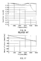
- FIG. 17 illustrates the frequency response of the amount of phase change caused by the third matching section 30 C.
- the horizontal axis represents frequency
- the vertical axis represents the amount of phase change.
- the third matching section 30 C causes a smaller change in the phase of a signal passing therethrough than the change caused by each of the first and second matching sections 30 A and 30 B given that signals passing therethrough have the same frequency.
- the absolute value of the amount of phase change becomes 180 degrees at a higher frequency when compared with the first and second matching sections 30 A and 30 B.
- FIG. 17 illustrates the frequency response of the amount of phase change caused by the third matching section 30 C.
- the horizontal axis represents frequency
- the vertical axis represents the amount of phase change.
- the absolute value of the amount of phase change becomes 180 degrees at a frequency of approximately 3800 MHz
- the absolute value of the amount of phase change becomes 180 degrees at a frequency above 5000 MHz.
- the absolute value of the amount of phase change caused by each of the first and second matching sections 30 A and 30 B and the absolute value of the amount of phase change caused by the third matching section 30 C preferably differ by 10 degrees or more.
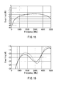
- FIG. 18 illustrates the frequency response of the coupling of the aforementioned coupler portion made up of the third coupling section 40 C, the fourth coupling section 40 D and the third matching section 30 C.
- the horizontal axis represents frequency
- the vertical axis represents coupling.
- two signal paths are formed between the input port and the coupling port in the coupler portion.
- the input port is the first port 11
- the coupling port is the first end 20 C 1 of the third subline section 20 C.
- One of the two signal paths runs through the third coupling section 40 C, and the other runs through the fourth coupling section 40 D and the third matching section 30 C.
- the coupling of the coupler portion increases with increasing frequency up to approximately 3000 MHz, and decreases with increasing frequency in a frequency range from approximately 3000 MHz to 5000 MHz. This is because, with increasing frequency in the frequency range shown on the horizontal axis of FIG. 18 , the coupling of each of the third and fourth coupling sections 40 C and 40 D alone increases, and on the other hand, the absolute value of the amount of phase change caused by the third matching section 30 C becomes closer to 180 degrees.
- a change in the coupling of the coupler portion in response to a change in frequency is reduced.
- a directional coupler configured by adding a stray capacitance of the first inductor to each of the first and second matching sections 30 A and 30 B in the directional coupler 1 will be referred to as a directional coupler of a first comparative example.
- FIG. 19 to FIG. 21 illustrate an example of characteristics of the directional coupler 1 according to the first embodiment and the directional coupler of the first comparative example.
- the service frequency band of the directional coupler 1 is 700 to 3800 MHz.
- the upper and lower limits of this service frequency band are shown by two dotted lines.
- the characteristics shown in FIG. 19 to FIG. 21 were determined by simulation.
- the solid line represents the characteristic of the directional coupler 1 used in the first mode of use
- the broken line represents the characteristic of the directional coupler of the first comparative example used in the first mode of use.
- the characteristic of the directional coupler 1 used in the second mode of use is the same as the characteristic of the directional coupler 1 used in the first mode of use
- the characteristic of the directional coupler of the first comparative example used in the second mode of use is the same as the characteristic of the directional coupler of the first comparative example used in the first mode of use.
- FIG. 19 illustrates the frequency response of the coupling of each of the directional coupler 1 and the directional coupler of the first comparative example.
- the horizontal axis represents frequency
- the vertical axis represents coupling. If we let ⁇ c (dB) denote coupling, the directional coupler 1 exhibits a sufficiently large value of c, that is, 20 or above, in the service frequency band.
- FIG. 20 illustrates the frequency response of the isolation of each of the directional coupler 1 and the directional coupler of the first comparative example.
- the horizontal axis represents frequency
- the vertical axis represents isolation. If we let ⁇ i (dB) denote isolation, the directional coupler 1 exhibits a sufficiently large value of i, that is, 45 or above, in the service frequency band.
- FIG. 21 illustrates the frequency response of the return loss at the coupling port of each of the directional coupler 1 and the directional coupler of the first comparative example.
- the horizontal axis represents frequency
- the vertical axis represents return loss at the coupling port.
- ⁇ r (dB) denote return loss at the coupling port
- the directional coupler 1 exhibits a sufficiently large value of r, that is, 20 or above, in the service frequency band. This means that the reflection coefficient as viewed in the direction from one of the third and fourth ports 13 and 14 to the other has an absolute value of zero or near zero in the service frequency band.
- the frequency response of the coupling of the directional coupler 1 shows a reduced change in coupling in response to a change in frequency over a wide frequency range.
- the frequency response of the coupling of the directional coupler of the first comparative example indicated by the broken line in FIG. 19 shows a greater change in coupling in response to a change in frequency when compared with the frequency response of the coupling of the directional coupler 1 . This is due to the stray capacitance of the first inductor in each of the first and second matching sections 30 A and 30 B.
- the directional coupler 1 is able to reduce a change in coupling in response to a change in frequency over a wide frequency range.
- the coupling of each of the third and fourth coupling sections 40 C and 40 D alone is higher than the coupling of each of the first and second coupling sections 40 A and 40 B alone.
- the frequency response of the coupling of the directional coupler 1 depends greatly on the frequency response of the coupling of the coupler portion shown in FIG. 18 .
- a signal having passed through the first coupling section 40 A and a signal having passed through the second coupling section 40 B are combined with a signal having passed through the coupler portion under the respective phase relationships determined at the first matching section 30 A and the second matching section 30 B to form a coupling signal.
- the frequency response of the coupling of the directional coupler 1 exhibits a reduced change in coupling in response to a change in frequency when compared with the frequency response of the coupling of the coupler portion shown in FIG. 18 .
- the absolute value of the amount of phase change becomes 180 degrees at a higher frequency when compared with the first and second matching sections 30 A and 30 B.
- the coupling of the coupler portion provides such a frequency response that a change in coupling in response to a change in frequency is reduced in a frequency range higher than the frequency at which the absolute value of the amount of phase change caused by each of the first and second matching sections 30 A and 30 B becomes 180 degrees.
- the directional coupler 1 makes it possible for the directional coupler 1 to reduce a change in coupling in response to a change in frequency even in a frequency range higher than the frequency at which the absolute value of the amount of phase change caused by each of the first and second matching sections 30 A and 30 B becomes 180 degrees.
- the directional coupler 1 is able to reduce a change in coupling in response to a change in frequency over a wide frequency range.
- the absolute value of the amount of phase change caused by each of the first and second matching sections 30 A and 30 B gets farther away from 180 degrees than a desired value in both of frequency ranges higher than and lower than the frequency at which the absolute value of the amount of phase change becomes 180 degrees.
- a change in coupling in response to a change in frequency increases.
- the inductor when an inductor is formed using a stack, the inductor will have a large stray capacitance in the cases where a plurality of conductor layers that form the inductor are arranged to overlap each other when viewed in the stacking direction, and where a relatively large conductor layer is present near one or more conductor layers that form the inductor.
- the entirety of the first inductor L 1 A excluding the connection portions 721 s and 721 e does not include portions that overlap each other when viewed in the stacking direction T.
- the entirety of the first inductor L 1 B excluding the connection portions 722 s and 722 e does not include portions that overlap each other when viewed in the stacking direction T.
- the first inductor L 1 A is located closer to the top surface 50 A than are the first and second capacitors C 1 A and C 2 A, the second inductor L 2 A, the main line 10 and the subline sections 20 A, 20 B, 20 C and 20 D.
- the first inductor L 1 B is located closer to the top surface 50 A than are the first and second capacitors C 1 B and C 2 B, the second inductor L 2 B, the main line 10 and the subline sections 20 A, 20 B, 20 C and 20 D.
- any conductor layer used for forming the directional coupler 1 is not present above the first inductors L 1 A and L 1 B. This also serves to prevent the first inductors L 1 A and L 1 B from having a large stray capacitance.
- the second inductor L 2 A is located closer to the bottom surface 50 B than are the first and second capacitors C 1 A and C 2 A.
- the second inductor L 2 B is located closer to the bottom surface 50 B than are the first and second capacitors C 1 B and C 2 B.
- the first embodiment makes it possible to prevent the first inductors L 1 A and L 1 B from having a large stray capacitance. As a result, it becomes possible to achieve a further reduction in a change in the coupling of the directional coupler 1 in response to a change in frequency.
- the directional coupler 1 according to the first embodiment is wideband capable.
- the directional coupler 1 according to the first embodiment is usable for multiple signals in multiple frequency bands used in CA.
- the directional coupler 1 can have symmetric or approximately symmetric circuitry. This allows the directional coupler 1 to be bidirectional.
- the third matching section 30 C causes a smaller change in the phase of the signal passing therethrough than the change caused by each of the first and second matching sections 30 A and 30 B.
- the third matching section 30 C can thus be formed easily, using a relatively short line. This makes it easier to construct the directional coupler 1 than in the case where the third matching section 30 C is formed using a plurality of inductors and a plurality of capacitors like the first and second matching sections 30 A and 30 B.
- any conductor layer that may obstruct the passage of magnetic flux generated by the first inductors L 1 A and L 1 B is not present above the first inductors L 1 A and L 1 B.
- the first inductors L 1 A and L 1 B can have sufficiently large inductances even if they are small in size. This allows for miniaturization of the directional coupler 1 .
- any conductor layer connected to the ground has a stray inductance lower than 0.1 nH.
- the circuitry of the directional coupling 1 may not be completely symmetric but need only be approximately symmetric.
- the directional coupler 1 can be wideband capable and bidirectional even if the circuitry thereof is not completely symmetric. Necessary conditions and preferable conditions for satisfying the requirement that the circuitry of the directional coupler 1 be approximately symmetric are specifically as follows, for example.
- the difference between the coupling of the first coupling section 40 A and the coupling of the second coupling section 40 B at a frequency of 2000 MHz needs to be 2 dB or less, and is preferably 1 dB or less.
- the difference between the amount of phase change caused by the first matching section 30 A and the amount of phase change caused by the second matching section 30 B at 2000 MHz needs to be 20 degrees or less, and is preferably 10 degrees or less, and more preferably 5 degrees or less.
- the difference between the coupling of the third coupling section 40 C and the coupling of the fourth coupling section 40 D at 2000 MHz needs to be 2 dB or less, and is preferably 1 dB or less.
- the directional coupler 101 includes a first port 11 , a second port 12 , a third port 13 , and a fourth port 14 .
- One of the third and fourth ports 13 and 14 is grounded via a terminator 15 having a resistance of, for example, 50 ⁇ .
- the directional coupler 101 further includes: a main line 110 connecting the first port 11 and the second port 12 ; N subline sections each of which is formed of a line configured to be electromagnetically coupled to the main line 110 ; (N ⁇ 1) matching section(s); and a stack for integrating the first to fourth ports 11 to 14 , the main line 110 , the N subline sections and the (N ⁇ 1) matching section(s).
- N is an integer of 2 or more.
- N is 3.
- the directional coupler 101 includes a first subline section 120 A, a second subline section 120 B, a third subline section 120 C, a first matching section 130 A, and a second matching section 130 B.
- the first subline section 120 A has a first end 120 A 1 and a second end 120 A 2 opposite to each other.
- the second subline section 120 B has a first end 120 B 1 and a second end 120 B 2 opposite to each other.
- the third subline section 120 C has a first end 120 C 1 and a second end 120 C 2 opposite to each other.
- the first matching section 130 A has a first end 130 A 1 and a second end 130 A 2 opposite to each other.
- the second matching section 130 B has a first end 130 B 1 and a second end 130 B 2 opposite to each other.
- the first end 120 A 1 of the first subline section 120 A is connected to the third port 13 .
- the first matching section 130 A is provided between the second end 120 A 2 of the first subline section 120 A and the first end 120 C 1 of the third subline section 120 C.
- the first end 130 A 1 of the first matching section 130 A is connected to the second end 120 A 2 of the first subline section 120 A.
- the first end 120 C 1 of the third subline section 120 C is connected to the second end 130 A 2 of the first matching section 130 A.
- the first end 120 B 1 of the second subline section 120 B is connected to the fourth port 14 .
- the second matching section 130 B is provided between the second end 120 B 2 of the second subline section 120 B and the second end 120 C 2 of the third subline section 120 C.
- the first end 130 B 1 of the second matching section 130 B is connected to the second end 120 B 2 of the second subline section 120 B.
- the second end 120 C 2 of the third subline section 120 C is connected to the second end 130 B 2 of the second matching section 130 B.
- the first matching section 130 A includes a first path 131 A connecting the first end 130 A 1 and the second end 130 A 2 , and a second path 132 A connecting the first path 131 A to the ground.
- the first path 131 A includes a first inductor L 101 A.
- the first inductor L 101 A has a first end L 101 A 1 and a second end L 101 A 2 opposite to each other.
- the first end L 101 A 1 is taken as the end closer to the first subline section 120 A
- the second end L 101 A 2 is taken as the end closer to the third subline section 120 C.
- the second path 132 A includes a first capacitor C 101 A and a second inductor L 102 A connected in series.
- the second inductor L 102 A has a first end L 102 A 1 and a second end L 102 A 2 .
- the first end L 102 A 1 is closest to the first path 131 A
- the second end L 102 A 2 is closest to the ground.
- the first capacitor C 101 A is provided between the first end L 101 A 1 of the first inductor L 101 A and the first end L 102 A 1 of the second inductor L 102 A.
- the second path 132 A further includes a second capacitor C 102 A provided between the second end L 101 A 2 of the first inductor L 101 A and the first end L 102 A 1 of the second inductor L 102 A.
- the second inductor L 102 A has an inductance of 0.1 nH or higher.
- the inductance of the second inductor L 102 A is preferably not higher than 7 nH.
- the circuitry of the second matching section 130 B is similar to that of the first matching section 130 A. More specifically, the second matching section 130 B includes a first path 131 B connecting the first end 130 B 1 and the second end 130 B 2 , and a second path 132 B connecting the first path 131 B to the ground.
- the first path 131 B includes a first inductor L 101 B.
- the first inductor L 101 B has a first end L 101 B and a second end L 101 B 2 opposite to each other.
- the first end L 101 B is taken as the end closer to the second subline section 120 B
- the second end L 101 B 2 is taken as the end closer to the third subline section 120 C.
- the second path 132 B includes a first capacitor C 101 B and a second inductor L 102 B connected in series.
- the second inductor L 102 B has a first end L 102 B 1 and a second end L 102 B 2 .
- the first end L 102 B 1 is closest to the first path 131 B
- the second end L 102 B 2 is closest to the ground.
- the first capacitor C 101 B is provided between the first end L 101 B 1 of the first inductor L 101 B and the first end L 102 B 1 of the second inductor L 102 B.
- the second path 132 B further includes a second capacitor C 102 B provided between the second end L 101 B 2 of the first inductor L 101 B and the first end L 102 B 1 of the second inductor L 102 B.
- the second inductor L 102 B has an inductance of 0.1 nH or higher.
- the inductance of the second inductor L 102 B is preferably not higher than 7 nH.
- first coupling section 140 A A combination of respective portions of the main line 110 and the first subline section 120 A coupled to each other will be referred to as the first coupling section 140 A.
- second coupling section 140 B A combination of respective portions of the main line 110 and the third subline section 130 C coupled to each other will be referred to as the third coupling section 140 C.
- the strengths of coupling of the first to third coupling sections 140 A, 140 B and 140 C will be defined as follows.
- the strength of coupling of the first coupling section 140 A is the strength of coupling of the first subline section 120 A to the main line 110 .
- the strength of coupling of the first coupling section 140 A is expressible in terms of the coupling of the first coupling section 140 A alone. The higher the coupling of the first coupling section 140 A alone, the higher the strength of coupling of the first coupling section 140 A.
- the strength of coupling of the second coupling section 140 B is the strength of coupling of the second subline section 120 B to the main line 110 .
- the strength of coupling of the second coupling section 140 B is expressible in terms of the coupling of the second coupling section 140 B alone. The higher the coupling of the second coupling section 140 B alone, the higher the strength of coupling of the second coupling section 140 B.
- the strength of coupling of the third coupling section 140 C is the strength of coupling of the third subline section 120 C to the main line 110 .
- the strength of coupling of the third coupling section 140 C is expressible in terms of the coupling of the third coupling section 140 C alone. The higher the coupling of the third coupling section 140 C alone, the higher the strength of coupling of the third coupling section 140 C.
- the third subline section 120 C is coupled more strongly to the main line 110 than are the first and second subline sections 120 A and 120 B.
- the strength of coupling of the third coupling section 140 C is higher than the strength of coupling of each of the first and second coupling sections 140 A and 140 B.
- Each of the first and second matching sections 130 A and 130 B is a circuit for performing impedance matching between a signal source and a load, assuming a situation in which one of the third and fourth ports 13 and 14 is grounded via a terminator serving as the load, and the other of the third and fourth ports 13 and 14 is connected with the signal source having an output impedance equal to the resistance of the terminator (e.g., 50 ⁇ ).
- the first and second matching sections 130 A and 130 B are each designed so that the reflection coefficient as viewed in the direction from one of the third and fourth ports 13 and 14 to the other has an absolute value of zero or near zero in the service frequency band of the directional coupler 101 .
- Each of the first and second matching sections 130 A and 130 B causes a change in the phase of a signal passing therethrough.
- the circuitry of the directional coupler 101 is preferably symmetric with respect to the third coupling section 140 C.
- the circuitry of the directional coupling 1 may not be completely symmetric, but need only be approximately symmetric.
- the circuitry of the directional coupler 1 is symmetric.
- the strength of coupling of the second coupling section 140 B is equal to the strength of coupling of the first coupling section 140 A.
- the circuitry of the first matching section 130 A and that of the second matching section 130 B, including element values, are mutually symmetric with respect to the third coupling section 140 C.
- the inductances of the first inductors L 101 A and L 101 B pairing up with each other are substantially equal to each other; the inductances of the second inductors L 102 A and L 102 B pairing up with each other are substantially equal to each other; the capacitances of the first capacitors C 101 A and C 101 B pairing up with each other are substantially equal to each other; and the capacitances of the second capacitors C 102 A and C 102 B pairing up with each other are substantially equal to each other.
- the first and second matching sections 130 A and 130 B cause changes of the same magnitude in the phase of those signals.
- the directional coupler 101 is bidirectional because the circuitry thereof is symmetric with respect to the third coupling section 140 C.
- the first capacitor C 101 A is provided between the first end L 101 A 1 of the first inductor L 101 A and the first end L 102 A 1 of the second inductor L 102 A
- the second capacitor C 102 A is provided between the second end L 101 A 2 of the first inductor L 101 A and the first end L 102 A 1 of the second inductor L 102 A.
- the first capacitor C 101 B is provided between the first end L 101 B 1 of the first inductor L 101 B and the first end L 102 B 1 of the second inductor L 102 B
- the second capacitor C 102 B is provided between the second end L 101 B 2 of the first inductor L 101 B and the first end L 102 B 1 of the second inductor L 102 B.
- the first and second capacitors C 101 A and C 102 A in the first matching section 130 A may be provided in a reversed arrangement from that in the example shown in FIG. 22 , and ditto for the first and second capacitors C 101 B and C 102 B in the second matching section 130 B.
- the first capacitor C 101 A may be provided between the second end L 101 A 2 of the first inductor L 101 A and the first end L 102 A 1 of the second inductor L 102 A
- the second capacitor C 102 A may be provided between the first end L 101 A 1 of the first inductor L 101 A and the first end L 102 A 1 of the second inductor L 102 A.
- the first capacitor C 101 B is provided between the second end L 101 B 2 of the first inductor L 101 B and the first end L 102 B 1 of the second inductor L 102 B
- the second capacitor C 102 B is provided between the first end L 101 B 1 of the first inductor L 101 B and the first end L 102 B 1 of the second inductor L 102 B.
- the operation of the directional coupler 101 according to the second embodiment will now be described.
- the directional coupler 101 is usable in the first and second modes of use described in relation to the first embodiment.
- a high frequency signal is received at the first port 11 and output from the second port 12 .
- the third port 13 outputs a coupling signal having a power that depends on the power of the high frequency signal received at the first port 11 .
- a first, a second and a third signal path are formed between the first port 11 serving as the input port and the third port 13 serving as the coupling port.
- the first signal path runs through the first coupling section 140 A.
- the second signal path runs through the third coupling section 140 C and the first matching section 130 A.
- the third signal path runs through the second coupling section 140 B, the second matching section 130 B and the first matching section 130 A.
- the coupling signal to be output from the third port 13 is a signal resulting from a combination of signals that have respectively passed through the first to third signal paths.
- the coupling of the directional coupler 101 used in the first mode of use depends on the strength of coupling of each of the first to third coupling sections 140 A, 140 B and 140 C and the relationship among the phases of the signals that have respectively passed through the first to third signal paths.
- a fourth, a fifth and a sixth signal path are formed between the second port 12 serving as the output port and the third port 13 serving as the coupling port.
- the fourth signal path runs through the first coupling section 140 A.
- the fifth signal path runs through the third coupling section 140 C and the first matching section 130 A.
- the sixth signal path runs through the second coupling section 140 B, the second matching section 130 B and the first matching section 130 A.
- the isolation of the directional coupler 101 used in the first mode of use depends on the strength of coupling of each of the first to third coupling sections 140 A, 140 B and 140 C and the relationship among the phases of signals that have respectively passed through the fourth to sixth signal paths.
- a high frequency signal is received at the second port 12 and output from the first port 11 .
- the fourth port 14 outputs a coupling signal having a power that depends on the power of the high frequency signal received at the second port 12 .
- a seventh, an eighth and a ninth signal path are formed between the second port 12 serving as the input port and the fourth port 14 serving as the coupling port.
- the seventh signal path runs through the second coupling section 140 B.
- the eighth signal path runs through the third coupling section 140 C and the second matching section 130 B.
- the ninth signal path runs through the first coupling section 140 A, the first matching section 130 A and the second matching section 130 B.
- the coupling signal to be output from the fourth port 14 is a signal resulting from a combination of signals that have respectively passed through the seventh to ninth signal paths.
- the coupling of the directional coupler 101 used in the second mode of use depends on the strength of coupling of each of the first to third coupling sections 140 A, 140 B and 140 C and the relationship among the phases of the signals that have respectively passed through the seventh to ninth signal paths.
- a tenth, an eleventh and a twelfth signal path are formed between the first port 11 serving as the output port and the fourth port 14 serving as the coupling port.
- the tenth signal path runs through the second coupling section 140 B.
- the eleventh signal path runs through the third coupling section 140 C and the second matching section 130 B.
- the twelfth signal path runs through the first coupling section 140 A, the first matching section 130 A and the second matching section 130 B.
- the isolation of the directional coupler 101 used in the second mode of use depends on the strength of coupling of each of the first to third coupling sections 140 A, 140 B and 140 C and the relationship among the phases of signals that have respectively passed through the tenth to twelfth signal paths.
- FIG. 23 is a perspective view of the directional coupler 101 .
- the directional coupler 101 shown in FIG. 23 includes a stack 150 for integrating the first to fourth ports 11 to 14 , the main line 110 , the first to third subline sections 120 A, 120 B and 120 C, and the first and second matching sections 130 A and 130 B.
- the stack 150 includes a plurality of dielectric layers and a plurality of conductor layers stacked on each other.
- Each of the inductors L 101 A, L 102 A, L 101 B and L 102 B is formed using one or more inductor-forming layers, which are one or more conductor layers among the plurality of conductor layers of the stack 150 .
- Each of the capacitors C 101 A, C 102 A, C 101 B and C 102 B is formed using two or more conductor layers among the plurality of conductor layers of the stack 150 .
- the stack 150 is shaped similarly to the stack 50 of the first embodiment. More specifically, the stack 150 is shaped like a rectangular solid and has a periphery.
- the periphery of the stack 150 includes a top surface 150 A, a bottom surface 150 B, and four side surfaces 150 C, 150 D, 150 E and 150 F.
- the top surface 150 A and the bottom surface 150 B are opposite each other.
- the side surfaces 150 C and 150 D are opposite each other.
- the side surfaces 150 E and 150 F are opposite each other.
- the side surfaces 150 C to 150 F are perpendicular to the top surface 150 A and the bottom surface 150 B.
- a direction perpendicular to the top surface 150 A and the bottom surface 150 B is the stacking direction of the plurality of dielectric layers and conductor layers.
- the stacking direction is shown by the arrow T in FIG. 23 .
- the top surface 150 A and the bottom surface 150 B are located at opposite ends in the stacking direction T.
- the directional coupler 101 shown in FIG. 23 has a first terminal 111 , a second terminal 112 , a third terminal 113 , a fourth terminal 114 , and two ground terminals 115 and 116 , like the directional coupler 1 of the first embodiment shown in FIG. 3 .
- the first to fourth terminals 111 , 112 , 113 and 114 correspond to the first to fourth ports 11 , 12 , 13 and 14 shown in FIG. 22 , respectively.
- the ground terminals 115 and 116 are connected to the ground.
- the terminals 111 to 116 are provided on the periphery of the stack 150 .
- the terminals 111 , 112 and 115 are arranged to extend from the top surface 150 A to the bottom surface 150 B through the side surface 150 C.
- the terminals 113 , 114 and 116 are arranged to extend from the top surface 150 A to the bottom surface 150 B through the side surface 150 D.
- the stack 150 will now be described in detail with reference to FIG. 24 to FIG. 31E .
- the stack 150 includes twenty-five dielectric layers stacked on top of one another. The twenty-five dielectric layers will be referred to as the first to twenty-fifth dielectric layers in the order from top to bottom.
- FIG. 24 is a perspective internal view of the stack 150 .
- FIG. 25 is a cross-sectional view of the stack 150 .
- FIG. 26A to FIG. 26D illustrate the respective patterned surfaces of the first to fourth dielectric layers.
- FIG. 27A to FIG. 27D illustrate the respective patterned surfaces of the fifth to eighth dielectric layers.
- FIG. 28A to FIG. 28D illustrate the respective patterned surfaces of the ninth to twelfth dielectric layers.
- FIG. 29D illustrate the respective patterned surfaces of the thirteenth to sixteenth dielectric layers.
- FIG. 30A to FIG. 30D illustrate the respective patterned surfaces of the seventeenth to twentieth dielectric layers.
- FIG. 31A to FIG. 31E illustrate the respective patterned surfaces of the twenty-first to twenty-fifth dielectric layers.
- a mark 1511 is formed on the patterned surface of the first dielectric layer 151 .
- inductor-forming layers 1521 and 1522 are formed on the patterned surface of the second dielectric layer 152 .
- the inductor-forming layers 1521 and 1522 are conductor layers used for forming the inductors L 101 A and L 101 B, respectively.
- Each of the inductor-forming layers 1521 and 1522 includes two connection portions for electrical connection to respective other elements, and a line portion connecting the two connection portions.
- the two connection portions of the inductor-forming layer 1521 will be denoted by symbols 1521 s and 1521 e .
- the line portion of the inductor-forming layer 1521 will be denoted by symbol 1521 L.
- the two connection portions of the inductor-forming layer 1522 will be denoted by symbols 1522 s and 1522 e .
- the line portion of the inductor-forming layer 1522 will be denoted by symbol 1522 L.
- through holes 152 T 3 , 152 T 4 , 152 T 5 and 152 T 6 are formed in the dielectric layer 152 .
- the through hole 152 T 3 is connected to the connection portion 1521 s of the inductor-forming layer 1521 .
- the through hole 152 T 4 is connected to the connection portion 1522 s of the inductor-forming layer 1522 .
- the through hole 152 T 5 is connected to the connection portion 1521 e of the inductor-forming layer 1521 .
- the through hole 152 T 6 is connected to the connection portion 1522 e of the inductor-forming layer 1522 .
- inductor-forming layers 1531 and 1532 are formed on the patterned surface of the third dielectric layer 153 .
- the inductor-forming layers 1531 and 1532 are conductor layers used for forming the inductors L 101 A and L 101 B, respectively.
- Each of the inductor-forming layers 1531 and 1532 includes two connection portions and a line portion, like the inductor-forming layers 1521 and 1522 .
- the two connection portions of the inductor-forming layer 1531 will be denoted by symbols 1531 s and 1531 e .
- the line portion of the inductor-forming layer 1531 will be denoted by symbol 1531 L.
- the two connection portions of the inductor-forming layer 1532 will be denoted by symbols 1532 s and 1532 e .
- the line portion of the inductor-forming layer 1532 will be denoted by symbol 1532 L.
- through holes 153 T 3 , 153 T 4 , 153 T 5 and 153 T 6 are formed in the dielectric layer 153 .
- the through hole 153 T 3 is connected to the connection portion 1531 s of the inductor-forming layer 1531 .
- the through hole 153 T 4 is connected to the connection portion 1532 s of the inductor-forming layer 1532 .
- the through holes 152 T 5 and 152 T 6 shown in FIG. 26B are connected to the through holes 153 T 5 and 153 T 6 , respectively.
- the through hole 152 T 3 shown in FIG. 26B is connected to the connection portion 1531 e of the inductor-forming layer 1531 .
- the through hole 152 T 4 shown in FIG. 26B is connected to the connection portion 1532 e of the inductor-forming layer 1532 .
- inductor-forming layers 1541 and 1542 are formed on the patterned surface of the fourth dielectric layer 154 .
- the inductor-forming layers 1541 and 1542 are conductor layers used for forming the inductors L 101 A and L 101 B, respectively.
- Each of the inductor-forming layers 1541 and 1542 includes two connection portions and a line portion, like the inductor-forming layers 1521 and 1522 .
- the two connection portions of the inductor-forming layer 1541 will be denoted by symbols 1541 s and 1541 e .
- the line portion of the inductor-forming layer 1541 will be denoted by symbol 1541 L.
- the two connection portions of the inductor-forming layer 1542 will be denoted by symbols 1542 s and 1542 e .
- the line portion of the inductor-forming layer 1542 will be denoted by symbol 1542 L.
- through holes 154 T 3 , 154 T 4 , 154 T 5 and 154 T 6 are formed in the dielectric layer 154 .
- the through hole 154 T 3 is connected to the connection portion 1541 s of the inductor-forming layer 1541 .
- the through hole 154 T 4 is connected to the connection portion 1542 s of the inductor-forming layer 1542 .
- the through holes 153 T 5 and 153 T 6 shown in FIG. 26C are connected to the through holes 154 T 5 and 154 T 6 , respectively.
- the through hole 153 T 3 shown in FIG. 26C is connected to the connection portion 1541 e of the inductor-forming layer 1541 .
- the through hole 153 T 4 shown in FIG. 26C is connected to the connection portion 1542 e of the inductor-forming layer 1542 .
- through holes 155 T 3 , 155 T 4 , 155 T 5 and 155 T 6 are formed in the fifth dielectric layer 155 .
- the through holes 154 T 3 to 154 T 6 shown in FIG. 26D are connected to the through holes 155 T 3 to 155 T 6 , respectively.
- conductor layers 1561 and 1562 are formed on the patterned surface of the sixth dielectric layer 156 .
- the conductor layers 1561 and 1562 are used for forming the capacitors C 102 A and C 102 B, respectively.
- through holes 156 T 3 , 156 T 4 , 156 T 5 , 156 T 6 , 156 T 7 and 156 T 8 are formed in the dielectric layer 156 .
- the through holes 155 T 3 to 155 T 6 shown in FIG. 27A are connected to the through holes 156 T 3 to 156 T 6 , respectively.
- the through hole 15617 is connected to the conductor layer 1561 .
- the through hole 156 T 8 is connected to the conductor layer 1562 .
- conductor layers 1571 and 1572 are formed on the patterned surface of the seventh dielectric layer 157 .
- the conductor layers 1571 and 1572 are used for forming the capacitors C 102 A and C 102 B, respectively.
- through holes 157 T 3 , 157 T 4 , 157 T 5 , 157 T 6 , 157 T 7 and 157 T 8 are formed in the dielectric layer 157 .
- the through holes 156 T 3 , 156 T 4 , 156 T 7 and 156 T 8 shown in FIG. 27B are connected to the through holes 157 T 3 , 157 T 4 , 15717 and 157 T 8 , respectively.
- the through hole 157 T 5 is connected to the conductor layer 1571 .
- the through hole 157 T 6 is connected to the conductor layer 1572 .
- conductor layers 1581 and 1582 are formed on the patterned surface of the eighth dielectric layer 158 .
- the conductor layer 1581 is used for forming the capacitors C 101 A and C 102 A.
- the conductor layer 1582 is used for forming the capacitors C 101 B and C 102 B.
- through holes 158 T 3 , 158 T 4 , 158 T 5 , 158 T 6 , 158 T 7 and 158 T 8 are formed in the dielectric layer 158 .
- the through holes 157 T 3 to 157 T 6 shown in FIG. 27C are connected to the through holes 158 T 3 to 158 T 6 , respectively.
- the through hole 158 T 7 is connected to the conductor layer 1581 and to the through hole 157 T 7 shown in FIG. 27C .
- the through hole 158 T 8 is connected to the conductor layer 1582 and to the through hole 157 T 8 shown in FIG. 27C .
- conductor layers 1591 and 1592 are formed on the patterned surface of the ninth dielectric layer 159 .
- the conductor layers 1591 and 1592 are used for forming the capacitors C 101 A and C 101 B, respectively.
- through holes 159 T 3 , 159 T 4 , 159 T 5 , 159 T 6 , 159 T 7 and 159 T 8 are formed in the dielectric layer 159 .
- the through hole 159 T 3 is connected to the conductor layer 1591 and to the through hole 158 T 3 shown in FIG. 27D .
- the through hole 159 T 4 is connected to the conductor layer 1592 and to the through hole 158 T 4 shown in FIG. 27D .
- the through holes 158 T 5 to 158 T 8 shown in FIG. 27D are connected to the through holes 159 T 5 to 159 T 8 , respectively.
- conductor layers 1601 and 1602 are formed on the patterned surface of the tenth dielectric layer 160 .
- the conductor layers 1601 and 1602 are used for forming the capacitors C 101 A and C 101 B, respectively.
- through holes 160 T 3 , 160 T 4 , 160 T 5 , 160 T 6 , 160 T 7 and 160 T 8 are formed in the dielectric layer 160 .
- the through holes 159 T 3 to 159 T 6 shown in FIG. 28A are connected to the through holes 160 T 3 to 160 T 6 , respectively.
- the through hole 159 T 7 shown in FIG. 28A and the through hole 160 T 7 are connected to the conductor layer 1601 .
- the through hole 159 T 8 shown in FIG. 28A and the through hole 160 T 8 are connected to the conductor layer 1602 .
- through holes 161 T 3 , 161 T 4 , 161 T 5 , 161 T 6 , 161 T 7 and 161 T 8 are formed in the eleventh dielectric layer 161 .
- the through holes 160 T 3 to 160 T 8 shown in FIG. 28B are connected to the through holes 161 T 3 to 161 T 8 , respectively.
- a conductor layer 1621 is formed on the patterned surface of the twelfth dielectric layer 162 .
- the conductor layer 1621 includes a line portion 1621 A forming the inductor L 102 A, a line portion 1621 B forming the inductor L 102 B, and a connection portion 1621 C connecting the line portions 1621 A and 1621 B.
- Each of the line portions 1621 A and 1621 B has a first end and a second end. The first end of the line portion 1621 A and the first end of the line portion 1621 B are connected to the connection portion 1621 C.
- through holes 162 T 3 , 162 T 4 , 162 T 5 , 162 T 6 and 162 T 9 are formed in the dielectric layer 162 .
- the through holes 161 T 3 to 161 T 6 shown in FIG. 28C are connected to the through holes 162 T 3 to 162 T 6 , respectively.
- the through hole 162 T 9 is connected to the connection portion 1621 C of the conductor layer 1621 .
- the through hole 161 T 7 shown in FIG. 28C is connected to a portion of the line portion 1621 A near the second end thereof.
- the through hole 161 T 8 shown in FIG. 28C is connected to a portion of the line portion 1621 B near the second end thereof.
- a ground conductor layer 1631 is formed on the patterned surface of the thirteenth dielectric layer 163 .
- the ground conductor layer 1631 is connected to the ground terminals 115 and 116 shown in FIG. 23 .
- through holes 163 T 3 , 163 T 4 , 163 T 5 and 163 T 6 are formed in the dielectric layer 163 .
- the through holes 162 T 3 to 162 T 6 shown in FIG. 28D are connected to the through holes 163 T 3 to 163 T 6 , respectively.
- the through hole 162 T 9 shown in FIG. 28D is connected to the ground conductor layer 1631 .
- through holes 164 T 3 , 164 T 4 , 164 T 5 and 164 T 6 are formed in the fourteenth dielectric layer 164 .
- the through holes 163 T 3 to 163 T 6 shown in FIG. 29A are connected to the through holes 164 T 3 to 164 T 6 , respectively.
- through holes 165 T 3 , 165 T 4 , 165 T 5 and 165 T 6 are formed in the fifteenth dielectric layer 165 .
- the through holes 164 T 3 to 164 T 6 shown in FIG. 29B are connected to the through holes 165 T 3 to 165 T 6 , respectively.
- through holes 166 T 3 , 166 T 4 , 166 T 5 and 166 T 6 are formed in the sixteenth dielectric layer 166 .
- the through holes 165 T 3 to 165 T 6 shown in FIG. 29C are connected to the through holes 166 T 3 to 166 T 6 , respectively.
- conductor layers 1671 and 1672 are formed on the patterned surface of the seventeenth dielectric layer 167 .
- the conductor layers 1671 and 1672 are used for forming the third subline section 120 C.
- Each of the conductor layers 1671 and 1672 has a first end and a second end.
- through holes 167 T 3 , 167 T 4 , 167 T 5 and 167 T 6 are formed in the dielectric layer 167 .
- the through holes 166 T 3 and 166 T 4 shown in FIG. 29D are connected to the through holes 167 T 3 and 167 T 4 , respectively.
- the through hole 167 T 5 is connected to a portion of the conductor layer 1671 near the first end thereof.
- the through hole 167 T 6 is connected to a portion of the conductor layer 1672 near the first end thereof.
- the through hole 166 T 5 shown in FIG. 29D is connected to a portion of the conductor layer 1671 near the second end thereof.
- the through hole 166 T 6 shown in FIG. 29D is connected to a portion of the conductor layer 1672 near the second end thereof.
- conductor layers 1681 and 1682 are formed on the patterned surface of the eighteenth dielectric layer 168 .
- the conductor layer 1681 is connected to the first terminal 111 shown in FIG. 23 .
- the conductor layer 1682 is connected to the second terminal 112 shown in FIG. 23 .
- through holes 168 T 1 , 16812 , 168 T 3 , 168 T 4 , 168 T 5 and 168 T 6 are formed in the dielectric layer 168 .
- the through hole 168 T 1 is connected to the conductor layer 1681 .
- the through hole 168 T 2 is connected to the conductor layer 1682 .
- the through holes 167 T 3 to 167 T 6 shown in FIG. 30A are connected to the through holes 168 T 3 to 168 T 6 , respectively.
- a conductor layer 1691 is formed on the patterned surface of the nineteenth dielectric layer 169 .
- the conductor layer 1691 is used for forming the main line 110 , and has a first end and a second end.
- through holes 169 T 3 , 169 T 4 , 169 T 5 and 169 T 6 are formed in the dielectric layer 169 .
- the through holes 168 T 3 to 168 T 6 shown in FIG. 30B are connected to the through holes 169 T 3 to 169 T 6 , respectively.
- the through hole 168 T 1 shown in FIG. 30B is connected to a portion of the conductor layer 1691 near the first end thereof.
- the through hole 168 T 2 shown in FIG. 30B is connected to a portion of the conductor layer 1691 near the second end thereof.
- through holes 170 T 3 , 170 T 4 , 170 T 5 and 170 T 6 are formed in the twentieth dielectric layer 170 .
- the through holes 169 T 3 to 169 T 6 shown in FIG. 30C are connected to the through holes 170 T 3 to 170 T 6 , respectively.
- a conductor layer 1711 is formed on the patterned surface of the twenty-first dielectric layer 171 .
- the conductor layer 1711 is used for forming the third subline section 120 C, and has a first end and a second end.
- through holes 171 T 3 and 171 T 4 are formed in the dielectric layer 171 .
- the through holes 170 T 3 and 170 T 4 shown in FIG. 30D are connected to the through holes 171 T 3 and 171 T 4 , respectively.
- the through hole 170 T 5 shown in FIG. 30D is connected to a portion of the conductor layer 1711 near the first end thereof.
- the through hole 170 T 6 shown in FIG. 30D is connected to a portion of the conductor layer 1711 near the second end thereof.
- conductor layers 1721 and 1722 are formed on the patterned surface of the twenty-second dielectric layer 172 .
- the conductor layers 1721 and 1722 are used for forming the first and second subline sections 120 A and 120 B, respectively.
- Each of the conductor layers 1721 and 1722 has a first end and a second end.
- through holes 172 T 3 and 172 T 4 are formed in the dielectric layer 172 .
- the through hole 172 T 3 is connected to a portion of the conductor layer 1721 near the first end thereof.
- the through hole 172 T 4 is connected to a portion of the conductor layer 1722 near the first end thereof.
- the through hole 171 T 3 shown in FIG. 31A is connected to a portion of the conductor layer 1721 near the second end thereof.
- the through hole 171 T 4 shown in FIG. 31A is connected to a portion of the conductor layer 1722 near the second end thereof.
- conductor layers 1731 and 1732 are formed on the patterned surface of the twenty-third dielectric layer 173 .
- the conductor layer 1731 is connected to the third terminal 113 shown in FIG. 23 .
- the conductor layer 1732 is connected to the fourth terminal 114 shown in FIG. 23 .
- the through hole 172 T 3 shown in FIG. 31B is connected to the conductor layer 1731 .
- the through hole 172 T 4 shown in FIG. 31B is connected to the conductor layer 1732 .
- no conductor layer is formed on the patterned surface of the twenty-fourth dielectric layer 174 .
- a ground conductor layer 1751 is formed on the patterned surface of the twenty-fifth dielectric layer 175 .
- the ground conductor layer 1751 is connected to the ground terminals 115 and 116 shown in FIG. 23 .
- the stack 150 shown in FIG. 23 is formed by stacking the first to twenty-fifth dielectric layers 151 to 175 so that the patterned surface of the first dielectric layer 151 also serves as the top surface 150 A of the stack 150 . Then, the terminals 111 to 116 are formed on the periphery of the stack 150 to complete the directional coupler 101 shown in FIG. 23 .
- FIG. 24 shows the interior of the stack 150 .
- FIG. 25 shows a cross section of the stack 150 as viewed from the side surface 150 C.
- the main line 110 is formed of the conductor layer 1691 shown in FIG. 30C .
- the conductor layer 1691 has a first surface facing toward the same direction as the patterned surface of the dielectric layer 169 , and a second surface opposite to the first surface.
- the first surface of the conductor layer 1691 includes a first portion and a second portion.
- the second surface of the conductor layer 1691 includes a third portion, a fourth portion and a fifth portion.
- a portion of the conductor layer 1721 shown in FIG. 31B is opposed to the third portion of the second surface of the conductor layer 1691 with the dielectric layers 169 , 170 and 171 interposed therebetween.
- the first subline section 120 A is formed of the aforementioned portion of the conductor layer 1721 .
- a portion of the conductor layer 1722 shown in FIG. 31B is opposed to the fourth portion of the second surface of the conductor layer 1691 with the dielectric layers 169 , 170 and 171 interposed therebetween.
- the second subline section 120 B is formed of the aforementioned portion of the conductor layer 1722 .
- the third subline section 120 C is formed as follows.
- the portion of the conductor layer 1671 ( FIG. 30A ) near the first end thereof is connected to the portion of the conductor layer 1711 ( FIG. 31A ) near the first end thereof via the through holes 167 T 5 , 168 T 5 , 169 T 5 and 170 T 5 .
- the portion of the conductor layer 1672 ( FIG. 30A ) near the first end thereof is connected to the portion of the conductor layer 1711 near the second end thereof via the through holes 167 T 6 , 168 T 6 , 169 T 6 and 170 T 6 .
- Part of the conductor layer 1671 is opposed to the first portion of the first surface of the conductor layer 1691 with the dielectric layers 167 and 168 interposed therebetween.
- Part of the conductor layer 1672 is opposed to the second portion of the first surface of the conductor layer 1691 with the dielectric layers 167 and 168 interposed therebetween.
- Part of the conductor layer 1711 is opposed to the fifth portion of the second surface of the conductor layer 1691 with the dielectric layers 169 and 170 interposed therebetween.
- the third subline section 120 C is formed of the aforementioned parts of the conductor layers 1671 , 1672 and 1711 .
- the inductor L 101 A of the first matching section 130 A is formed as follows.
- the inductor-forming layers 1521 , 1531 and 1541 shown in FIG. 26B to FIG. 26D are connected to each other in series via the through holes 152 T 3 and 153 T 3 .
- the inductor L 101 A is formed of these inductor-forming layers 1521 , 1531 and 1541 and the two through holes 152 T 3 and 153 T 3 connecting them.
- the inductor-forming layer 1541 is connected to the conductor layer 1721 forming the first subline section 120 A via the through holes 154 T 3 , 155 T 3 , 156 T 3 , 157 T 3 , 158 T 3 , 159 T 3 , 160 T 3 , 161 T 3 , 162 T 3 , 163 T 3 , 164 T 3 , 165 T 3 , 166 T 3 , 167 T 3 , 168 T 3 , 169 T 3 , 170 T 3 and 171 T 3 .
- the inductor-forming layer 1521 is connected to the conductor layer 1671 forming the third subline section 120 C via the through holes 152 T 5 , 153 T 5 , 154 T 5 , 155 T 5 , 156 T 5 , 157 T 5 , 158 T 5 , 159 T 5 , 160 T 5 , 161 T 5 , 162 T 5 , 163 T 5 , 164 T 5 , 165 T 5 and 166 T 5 .
- the capacitor C 101 A of the first matching section 130 A is formed of the conductor layers 1581 , 1591 and 1601 shown in FIGS. 27D, 28A and 28B , the dielectric layer 158 interposed between the conductor layers 1581 and 1591 , and the dielectric layer 159 interposed between the conductor layers 1591 and 1601 .
- the conductor layer 1591 is connected to the conductor layer 1721 forming the first subline section 120 A via the through holes 159 T 3 , 16013 , 161 T 3 , 162 T 3 , 163 T 3 , 164 T 3 , 165 T 3 , 166 T 3 , 167 T 3 , 168 T 3 , 169 T 3 , 170 T 3 and 171 T 3 .
- the capacitor C 102 A of the first matching section 130 A is formed of the conductor layers 1561 , 1571 and 1581 shown in FIG. 27B to FIG. 27D , the dielectric layer 156 interposed between the conductor layers 1561 and 1571 , and the dielectric layer 157 interposed between the conductor layers 1571 and 1581 .
- the conductor layer 1571 is connected to the conductor layer 1671 forming the third subline section 120 C via the through holes 157 T 5 , 158 T 5 , 159 T 5 , 160 T 5 , 161 T 5 , 162 T 5 , 163 T 5 , 164 T 5 , 165 T 5 and 166 T 5 .
- the inductor L 102 A of the first matching section 130 A is formed of the line portion 1621 A of the the conductor layer 1621 shown in FIG. 28D .
- the first end of the line portion 1621 A is connected to the ground conductor layer 1631 shown in FIG. 29A via the connection portion 1621 C and the through hole 162 T 9 .
- the portion of the line portion 1621 A near the second end thereof is connected to the conductor layer 1601 shown in FIG. 28B via the through holes 160 T 7 and 161 T 7 , and connected to the conductor layers 1561 and 1581 shown in FIG. 27B and FIG. 27D via the through holes 156 T 7 , 157 T 7 , 158 T 7 and 159 T 7 , the conductor layer 1601 and the through holes 160 T 7 and 161 T 7 .
- the inductor L 101 B of the second matching section 130 B is formed as follows.
- the inductor-forming layers 1522 , 1532 and 1542 shown in FIG. 26B to FIG. 26D are connected to each other in series via the through holes 152 T 4 and 153 T 4 .
- the inductor L 101 B is formed of these inductor-forming layers 1522 , 1532 and 1542 and the two through holes 152 T 4 and 153 T 4 connecting them.
- the inductor-forming layer 1542 is connected to the conductor layer 1722 forming the second subline section 120 B via the through holes 154 T 4 , 155 T 4 , 156 T 4 , 157 T 4 , 158 T 4 , 159 T 4 , 160 T 4 , 161 T 4 , 162 T 4 , 163 T 4 , 164 T 4 , 165 T 4 , 166 T 4 , 167 T 4 , 168 T 4 , 169 T 4 , 170 T 4 and 171 T 4 .
- the inductor-forming layer 1522 is connected to the conductor layer 1672 forming the third subline section 120 C via the through holes 152 T 6 , 153 T 6 , 154 T 6 , 155 T 6 , 156 T 6 , 157 T 6 , 158 T 6 , 159 T 6 , 160 T 6 , 161 T 6 , 162 T 6 , 163 T 6 , 164 T 6 , 165 T 6 and 166 T 6 .
- the capacitor C 101 B of the second matching section 130 B is formed of the conductor layers 1582 , 1592 and 1602 shown in FIGS. 27D, 28A and 28B , the dielectric layer 158 interposed between the conductor layers 1582 and 1592 , and the dielectric layer 159 interposed between the conductor layers 1592 and 1602 .
- the conductor layer 1592 is connected to the conductor layer 1722 forming the second subline section 120 B via the through holes 159 T 4 , 160 T 4 , 161 T 4 , 162 T 4 , 163 T 4 , 164 T 4 , 165 T 4 , 166 T 4 , 167 T 4 , 168 T 4 , 169 T 4 , 170 T 4 and 171 T 4 .
- the capacitor C 102 B of the second matching section 130 B is formed of the conductor layers 1562 , 1572 and 1582 shown in FIG. 27B to FIG. 27D , the dielectric layer 156 interposed between the conductor layers 1562 and 1572 , and the dielectric layer 157 interposed between the conductor layers 1572 and 1582 .
- the conductor layer 1572 is connected to the conductor layer 1672 forming the third subline section 120 C via the through holes 157 T 6 , 158 T 6 , 159 T 6 , 160 T 6 , 161 T 6 , 162 T 6 , 163 T 6 , 164 T 6 , 165 T 6 and 166 T 6 .
- the inductor L 102 B of the second matching section 130 B is formed of the line portion 1621 B of the the conductor layer 1621 shown in FIG. 28D .
- the first end of the line portion 1621 B is connected to the ground conductor layer 1631 shown in FIG. 29A via the connection portion 1621 C and the through hole 162 T 9 .
- the portion of the line portion 1621 B near the second end thereof is connected to the conductor layer 1602 shown in FIG. 28B via the through holes 160 T 8 and 161 T 8 , and connected to the conductor layers 1562 and 1582 shown in FIG. 27B and FIG. 27D via the through holes 156 T 8 , 157 T 8 , 158 T 8 and 159 T 8 , the conductor layer 1602 and the through holes 160 T 8 and 161 T 8 .
- the ground conductor layer 1631 connected to the ground is interposed between the conductor layer 1691 forming the main line 110 and the conductor layers forming the first and second matching sections 130 A and 130 B.
- the first and second matching sections 130 A and 130 B are not configured to be electromagnetically coupled to the main line 110 .
- the ground conductor layer 1751 shown in FIG. 31E has the function of adjusting the impedance of each of the first and second subline sections 120 A and 120 B to a desired value.
- the plurality of conductor layers of the stack 150 include a plurality of inductor-forming layers which are a plurality of conductor layers used to form the first inductor L 101 A of the first matching section 130 A, and another plurality of inductor-forming layers which are a plurality of conductor layers used to form the first inductor L 101 B of the second matching section 130 B.
- the first inductor L 101 A is formed of three inductor-forming layers 1521 , 1531 and 1541 connected in series; and the first inductor L 101 B is formed of three inductor-forming layers 1522 , 1532 and 1542 connected in series.
- Each of the inductor-forming layers 1521 , 1531 and 1541 includes two connection portions for electrical connection to respective other elements, and a line portion connecting the two connection portions.
- each of the inductor-forming layers 1522 , 1532 and 1542 includes two connection portions for electrical connection to respective other elements, and a line portion connecting the two connection portions.
- the inductor-forming layers 1521 , 1531 and 1541 forming the first inductor L 101 A are arranged such that their respective line portions do not overlap each other when viewed in the stacking direction T.
- the entirety of the first inductor L 101 A excluding the connection portions does not include portions that overlap each other when viewed in stacking direction T.
- the entirety of the first inductor L 101 A has a spiral shape when viewed in the stacking direction T.
- the three-dimensional shape of the entirety of the first inductor L 101 A is like a square frustum.
- the inductor-forming layers 1522 , 1532 and 1542 forming the first inductor L 101 B are arranged such that their respective line portions do not overlap each other when viewed in the stacking direction T.
- the entirety of the first inductor L 101 B excluding the connection portions does not include portions that overlap each other when viewed in stacking direction T.
- the entirety of the first inductor L 101 B has a spiral shape when viewed in the stacking direction T.
- the three-dimensional shape of the entirety of the first inductor L 101 B is like a square frustum.
- the first inductor L 101 A is located closer to the top surface 150 A than are the first and second capacitors C 101 A and C 102 A, the second inductor L 102 A, the main line 110 and the subline sections 120 A, 120 B and 120 C.
- the second inductor L 102 A is located closer to the bottom surface 150 B than are the first and second capacitors C 101 A and C 102 A.
- first inductor L 101 B is located closer to the top surface 150 A than are the first and second capacitors C 101 B and C 102 B, the second inductor L 102 B, the main line 110 and the subline sections 120 A, 120 B and 120 C.
- the second inductor L 102 B is located closer to the bottom surface 150 B than are the first and second capacitors C 101 B and C 102 B.
- the directional coupler 101 makes it possible to reduce a change in coupling in response to a change in frequency over a wide frequency band. This will be described in detail below.
- the coupling of each of the first to third coupling sections 140 A, 140 B and 140 C alone increases with increasing frequency.
- the coupling of the third coupling section 140 C alone is higher than the coupling of each of the first and second coupling sections 140 A and 140 B alone.
- the amount by which each of the first and second matching sections 130 A and 130 B changes the phase of a signal passing therethrough will be referred to as the amount of phase change.
- the amount of phase change is expressed in negative values because each of the matching sections 130 A and 130 B causes a phase delay of the signal passing therethrough. It can be said that the larger the absolute value of the amount of phase change, the greater is the change caused by each of the matching sections 130 A and 130 B in the phase of the signal passing therethrough.
- the matching sections 130 A and 130 B are configured in the same manner as the matching sections 30 A and 30 B of the first embodiment.
- a matching section configured by adding a stray capacitance of the first inductor L 101 A to the first matching section 130 A will be referred to as a matching section of a second comparative example.
- the stray capacitance is connected to the first inductor L 101 A in parallel.
- FIG. 32 illustrates the frequency response of the amount of phase change caused by each of the first matching section 130 A and the matching section of the second comparative example.
- the horizontal axis represents frequency
- the vertical axis represents the amount of phase change.
- the solid line represents the frequency response for the first matching section 130 A
- the broken line represents the frequency response for the matching section of the second comparative example.
- FIG. 33 illustrates the frequency response of the return loss of each of the first matching section 130 A and the matching section of the second comparative example.
- the horizontal axis represents frequency
- the vertical axis represents return loss.
- the solid line represents the frequency response for the first matching section 130 A
- the broken line represents the frequency response for the matching section of the second comparative example.
- FIG. 34 illustrates the frequency response of the insertion loss of each of the first matching section 130 A and the matching section of the second comparative example.
- the horizontal axis represents frequency
- the vertical axis represents insertion loss.
- the solid line represents the frequency response for the first matching section 130 A
- the broken line represents the frequency response for the matching section of the second comparative example.
- the characteristics of the first matching section 130 A change from the desired characteristics shown by the solid lines in FIGS. 32-34 to the characteristics of the matching section of the second comparative example shown by the broken lines in FIGS. 32-34 .
- a particular concern raised by the stray capacitance of the first inductor L 101 A is that the frequency response of the amount of phase change caused by the first matching section 130 A undergoes the following changes. As shown in FIG.
- the absolute value of the amount of phase change becomes smaller than a desired value in a frequency region lower than the frequency at which the absolute value of the amount of phase change is 180 degrees, and becomes larger than the desired value in a frequency region higher than the frequency at which the absolute value of the amount of phase change is 180 degrees.
- the second matching section 130 B has the same or almost the same characteristics as the first matching section 130 A. As is the case with the first matching section 130 A, if the first inductor L 101 B in the second matching section 130 B has a stray capacitance, the characteristics of the second matching section 130 B change from the desired characteristics to the characteristics of the matching section of the second comparative example. As will be shown later, if the first inductor in each of the first and second matching sections 130 A and 130 B has a stray capacitance, the directional coupler 101 has a reduced effect of reducing a change in coupling in response to a change in frequency.
- a directional coupler configured by adding a stray capacitance of the first inductor to each of the first and second matching sections 130 A and 130 B in the directional coupler 101 will be referred to as a directional coupler of a second comparative example.
- FIG. 35 to FIG. 37 illustrate an example of characteristics of the directional coupler 101 according to the second embodiment and the directional coupler of the second comparative example.
- the service frequency band of the directional coupler 101 is 700 to 2700 MHz.
- the upper and lower limits of this service frequency band are shown by two dotted lines.
- the characteristics shown in FIG. 35 to FIG. 37 were determined by simulation.
- the solid line represents the characteristic of the directional coupler 101 used in the first mode of use
- the broken line represents the characteristic of the directional coupler of the second comparative example used in the first mode of use.
- the characteristic of the directional coupler 101 used in the second mode of use is the same as the characteristic of the directional coupler 101 used in the first mode of use
- the characteristic of the directional coupler of the second comparative example used in the second mode of use is the same as the characteristic of the directional coupler of the second comparative example used in the first mode of use.
- FIG. 35 illustrates the frequency response of the coupling of each of the directional coupler 101 and the directional coupler of the second comparative example.
- the horizontal axis represents frequency
- the vertical axis represents coupling. If we let ⁇ c (dB) denote coupling, the directional coupler 101 exhibits a sufficiently large value of c, that is, 20 or above, in the service frequency band.
- FIG. 36 illustrates the frequency response of the isolation of each of the directional coupler 101 and the directional coupler of the second comparative example.
- the horizontal axis represents frequency
- the vertical axis represents isolation. If we let ⁇ i (dB) denote isolation, the directional coupler 101 exhibits a sufficiently large value of i, that is, 45 or above, in the service frequency band.
- FIG. 37 illustrates the frequency response of the return loss at the coupling port of each of the directional coupler 101 and the directional coupler of the second comparative example.
- the horizontal axis represents frequency
- the vertical axis represents return loss at the coupling port.
- ⁇ r (dB) denote return loss at the coupling port
- the directional coupler 101 exhibits a sufficiently large value of r, that is, 25 or above, in the service frequency band. This means that the reflection coefficient as viewed in the direction from one of the third and fourth ports 13 and 14 to the other has an absolute value of zero or near zero in the service frequency band.
- the frequency response of the coupling of the directional coupler 101 shows a reduced change in coupling in response to a change in frequency over a wide frequency range.
- the frequency response of the coupling of the directional coupler of the second comparative example indicated by the broken line in FIG. 35 shows a greater change in coupling in response to a change in frequency when compared with the frequency response of the coupling of the directional coupler 101 . This is due to the stray capacitance of the first inductor in each of the first and second matching sections 130 A and 130 B.
- the directional coupler 101 is able to reduce a change in coupling in response to a change in frequency over a wide frequency range.
- the coupling of the third coupling section 140 C alone is higher than the coupling of each of the first and second coupling sections 140 A and 140 B alone.
- a signal having passed through the first coupling section 140 A and a signal having passed through the second coupling section 140 B are combined with a signal having passed through the third coupling section 140 C under the respective phase relationships determined at the first matching section 130 A and the second matching section 130 B to form a coupling signal.
- the frequency response of the coupling of the directional coupler 101 exhibits a reduced change in coupling in response to a change in frequency when compared with the frequency response of the coupling of the third coupling section 140 C alone.
- the absolute value of the amount of phase change caused by each of the first and second matching sections 130 A and 130 B gets farther away from 180 degrees than a desired value in both of frequency ranges higher than and lower than the frequency at which the absolute value of the amount of phase change becomes 180 degrees.
- a change in coupling in response to a change in frequency increases.
- the entirety of the first inductor L 101 A excluding the connection portions does not include portions that overlap each other when viewed in the stacking direction T.
- the entirety of the first inductor L 101 B excluding the connection portions does not include portions that overlap each other when viewed in the stacking direction T.
- the first inductor L 101 A is located closer to the top surface 150 A than are the first and second capacitors C 101 A and C 102 A, the second inductor L 102 A, the main line 110 and the subline sections 120 A, 120 B and 120 C.
- the first inductor L 101 B is located closer to the top surface 150 A than are the first and second capacitors C 101 B and C 102 B, the second inductor L 102 B, the main line 110 and the subline sections 120 A, 120 B and 120 C.
- any conductor layer used for forming the directional coupler 101 is not present above the first inductors L 101 A and L 101 B. This also serves to prevent the first inductors L 101 A and L 101 B from having a large stray capacitance.
- the second inductor L 102 A is located closer to the bottom surface 150 B than are the first and second capacitors C 101 A and C 102 A.
- the second inductor L 102 B is located closer to the bottom surface 150 B than are the first and second capacitors C 101 B and C 102 B.
- the second embodiment makes it possible to prevent the first inductors L 101 A and L 101 B from having a large stray capacitance. As a result, it becomes possible to achieve a further reduction in a change in the coupling of the directional coupler 101 in response to a change in frequency.
- the directional coupler 101 is wideband capable. Further, as mentioned previously, the directional coupler 101 can have symmetric or approximately symmetric circuitry. This allows the directional coupler 101 to be bidirectional.
- any conductor layer that may obstruct the passage of magnetic flux generated by the first inductors L 101 A and L 101 B is not present above the first inductors L 101 A and L 101 B.
- the first inductors L 101 A and L 101 B can have sufficiently large inductances even if they are small in size. This allows for miniaturization of the directional coupler 101 .
- the present invention is not limited to the foregoing embodiments, and various modifications may be made thereto.
- the third matching section 30 C may have the same configuration as the first and second matching sections 30 A and 30 B, excluding element values.
- the number of the subline sections, N may be any integer of 2 or more. If N is 2, the directional coupler is provided with a first and a second subline section and a matching section, and the matching section is configured to satisfy the requirements concerning the (N ⁇ 1) matching section or at least one of the (N ⁇ 1) matching sections recited in the appended claims. If N is 3 or more, at least one of the three matching sections is configured to satisfy the requirements concerning at least one of the (N ⁇ 1) matching sections recited in the appended claims.
- the second inductor may be located closer to the bottom surface of the stack than are the first capacitor, the main line and the N subline sections.
Landscapes
- Engineering & Computer Science (AREA)
- Power Engineering (AREA)
- Transmitters (AREA)
- Amplifiers (AREA)
- Near-Field Transmission Systems (AREA)
Abstract
Description
C=10 log(P3/P1)[dB]
I=10 log(P03/P02)[dB]
RL=10 log(P6/P5)[dB]
Claims (7)
Applications Claiming Priority (2)
| Application Number | Priority Date | Filing Date | Title |
|---|---|---|---|
| JP2015156653A JP2017038115A (en) | 2015-08-07 | 2015-08-07 | Directional coupler |
| JP2015-156653 | 2015-08-07 |
Publications (2)
| Publication Number | Publication Date |
|---|---|
| US20170040661A1 US20170040661A1 (en) | 2017-02-09 |
| US9893408B2 true US9893408B2 (en) | 2018-02-13 |
Family
ID=58047966
Family Applications (1)
| Application Number | Title | Priority Date | Filing Date |
|---|---|---|---|
| US15/206,614 Expired - Fee Related US9893408B2 (en) | 2015-08-07 | 2016-07-11 | Directional coupler |
Country Status (3)
| Country | Link |
|---|---|
| US (1) | US9893408B2 (en) |
| JP (1) | JP2017038115A (en) |
| CN (1) | CN106450641A (en) |
Cited By (6)
| Publication number | Priority date | Publication date | Assignee | Title |
|---|---|---|---|---|
| US20180337439A1 (en) * | 2017-05-19 | 2018-11-22 | Murata Manufacturing Co., Ltd. | Directional coupler, high-frequency front-end module, and communication device |
| US10276913B2 (en) * | 2016-10-31 | 2019-04-30 | Tdk Corporation | Directional coupler |
| US10276912B2 (en) * | 2016-10-31 | 2019-04-30 | Tdk Corporation | Directional coupler |
| US10340575B2 (en) * | 2015-07-14 | 2019-07-02 | Murata Manufacturing Co., Ltd. | Directional coupler |
| RU208413U1 (en) * | 2021-06-28 | 2021-12-16 | Акционерное общество Омское производственное объединение "Радиозавод им. А.С. Попова" (РЕЛЕРО) | BROADBAND DIRECTIONAL COUPLER |
| US20240128629A1 (en) * | 2022-10-14 | 2024-04-18 | Murata Manufacturing Co., Ltd. | Directional coupler, high frequency module, and communication apparatus |
Families Citing this family (12)
| Publication number | Priority date | Publication date | Assignee | Title |
|---|---|---|---|---|
| JP6137507B2 (en) * | 2015-01-27 | 2017-05-31 | Tdk株式会社 | Directional coupler |
| JP6172479B2 (en) * | 2015-07-29 | 2017-08-02 | Tdk株式会社 | Directional coupler |
| JP6593192B2 (en) * | 2016-01-26 | 2019-10-23 | Tdk株式会社 | Directional coupler |
| WO2017158974A1 (en) * | 2016-03-18 | 2017-09-21 | 株式会社村田製作所 | Directional coupler |
| JP7155499B2 (en) * | 2017-04-26 | 2022-10-19 | Tdk株式会社 | LAMINATED ELECTRONIC COMPONENT AND MANUFACTURING METHOD THEREOF |
| WO2019054285A1 (en) | 2017-09-13 | 2019-03-21 | 株式会社村田製作所 | HIGH FREQUENCY MODULE |
| WO2020139407A1 (en) * | 2018-12-28 | 2020-07-02 | Google Llc | Attenuator for qubit drive signals |
| KR102810591B1 (en) | 2019-04-15 | 2025-05-22 | 삼성전자주식회사 | Directional coupler and electronic device including thereof |
| TWI730372B (en) * | 2019-08-07 | 2021-06-11 | 瑞昱半導體股份有限公司 | Wireless transmission circuit and control method thereof |
| JP7447506B2 (en) * | 2020-01-27 | 2024-03-12 | Tdk株式会社 | directional coupler |
| JP7505601B2 (en) * | 2021-01-29 | 2024-06-25 | 株式会社村田製作所 | Directional Coupler |
| JP7513344B2 (en) * | 2021-03-11 | 2024-07-09 | Tdk株式会社 | Multilayer Electronic Components |
Citations (7)
| Publication number | Priority date | Publication date | Assignee | Title |
|---|---|---|---|---|
| US7042309B2 (en) * | 2003-12-08 | 2006-05-09 | Werlatone, Inc. | Phase inverter and coupler assembly |
| US9000864B2 (en) * | 2013-06-26 | 2015-04-07 | Murata Manufacturing Co., Ltd. | Directional coupler |
| US9077061B2 (en) | 2011-06-14 | 2015-07-07 | Murata Manufacturing Co., Ltd. | Directional coupler |
| US9385411B2 (en) * | 2014-03-12 | 2016-07-05 | Tdk Corporation | Directional coupler |
| US9391354B2 (en) * | 2014-02-18 | 2016-07-12 | Tdk Corporation | Directional coupler |
| US9614269B2 (en) * | 2014-12-10 | 2017-04-04 | Skyworks Solutions, Inc. | RF coupler with adjustable termination impedance |
| US9653771B2 (en) * | 2015-01-27 | 2017-05-16 | Tdk Corporation | Directional coupler |
Family Cites Families (7)
| Publication number | Priority date | Publication date | Assignee | Title |
|---|---|---|---|---|
| JPH03250908A (en) * | 1990-02-28 | 1991-11-08 | Tdk Corp | High frequency amplifier added with filter |
| JP2002368553A (en) * | 2001-06-08 | 2002-12-20 | Mitsubishi Electric Corp | High frequency amplifier and wireless transmission device using the same |
| JP4530866B2 (en) * | 2005-02-09 | 2010-08-25 | 京セラ株式会社 | Filter element and electronic module |
| JP2007243559A (en) * | 2006-03-08 | 2007-09-20 | Mitsumi Electric Co Ltd | Antenna module and antenna device |
| CN201509200U (en) * | 2009-06-22 | 2010-06-16 | 摩比天线技术(深圳)有限公司 | Directional coupler and signal detection system |
| JP6080584B2 (en) * | 2013-02-08 | 2017-02-15 | 三菱電機株式会社 | Directional coupler |
| JP2015103957A (en) * | 2013-11-25 | 2015-06-04 | 三菱電機株式会社 | Impedance matching circuit and high-frequency amplifier |
-
2015
- 2015-08-07 JP JP2015156653A patent/JP2017038115A/en active Pending
-
2016
- 2016-07-11 US US15/206,614 patent/US9893408B2/en not_active Expired - Fee Related
- 2016-08-08 CN CN201610642994.6A patent/CN106450641A/en active Pending
Patent Citations (7)
| Publication number | Priority date | Publication date | Assignee | Title |
|---|---|---|---|---|
| US7042309B2 (en) * | 2003-12-08 | 2006-05-09 | Werlatone, Inc. | Phase inverter and coupler assembly |
| US9077061B2 (en) | 2011-06-14 | 2015-07-07 | Murata Manufacturing Co., Ltd. | Directional coupler |
| US9000864B2 (en) * | 2013-06-26 | 2015-04-07 | Murata Manufacturing Co., Ltd. | Directional coupler |
| US9391354B2 (en) * | 2014-02-18 | 2016-07-12 | Tdk Corporation | Directional coupler |
| US9385411B2 (en) * | 2014-03-12 | 2016-07-05 | Tdk Corporation | Directional coupler |
| US9614269B2 (en) * | 2014-12-10 | 2017-04-04 | Skyworks Solutions, Inc. | RF coupler with adjustable termination impedance |
| US9653771B2 (en) * | 2015-01-27 | 2017-05-16 | Tdk Corporation | Directional coupler |
Cited By (8)
| Publication number | Priority date | Publication date | Assignee | Title |
|---|---|---|---|---|
| US10340575B2 (en) * | 2015-07-14 | 2019-07-02 | Murata Manufacturing Co., Ltd. | Directional coupler |
| US10276913B2 (en) * | 2016-10-31 | 2019-04-30 | Tdk Corporation | Directional coupler |
| US10276912B2 (en) * | 2016-10-31 | 2019-04-30 | Tdk Corporation | Directional coupler |
| US20180337439A1 (en) * | 2017-05-19 | 2018-11-22 | Murata Manufacturing Co., Ltd. | Directional coupler, high-frequency front-end module, and communication device |
| US10756408B2 (en) * | 2017-05-19 | 2020-08-25 | Murata Manufacturing Co., Ltd. | Directional coupler, high-frequency front-end module, and communication device |
| RU208413U1 (en) * | 2021-06-28 | 2021-12-16 | Акционерное общество Омское производственное объединение "Радиозавод им. А.С. Попова" (РЕЛЕРО) | BROADBAND DIRECTIONAL COUPLER |
| US20240128629A1 (en) * | 2022-10-14 | 2024-04-18 | Murata Manufacturing Co., Ltd. | Directional coupler, high frequency module, and communication apparatus |
| US12614831B2 (en) * | 2022-10-14 | 2026-04-28 | Murata Manufacturing Co., Ltd. | Directional coupler, high frequency module, and communication apparatus |
Also Published As
| Publication number | Publication date |
|---|---|
| JP2017038115A (en) | 2017-02-16 |
| CN106450641A (en) | 2017-02-22 |
| US20170040661A1 (en) | 2017-02-09 |
Similar Documents
| Publication | Publication Date | Title |
|---|---|---|
| US9893408B2 (en) | Directional coupler | |
| US9893407B2 (en) | Directional coupler | |
| US9391354B2 (en) | Directional coupler | |
| US9653771B2 (en) | Directional coupler | |
| US10084225B2 (en) | Directional coupler | |
| US8314663B2 (en) | Directional coupler | |
| JP6346327B2 (en) | Duplexer | |
| US9413336B2 (en) | Multiband-support radio-frequency module | |
| CN103119782A (en) | circuit device | |
| US20130157587A1 (en) | Integrated circuit comprising an integrated transformer of the "balun" type with several input and output channels | |
| KR101926408B1 (en) | High-frequency switch module | |
| US10714806B2 (en) | Bi-directional coupler | |
| CN114175396B (en) | Balun | |
| US10998876B2 (en) | Balun | |
| US9871500B2 (en) | Multilayer electronic component | |
| US12388162B2 (en) | Marchand balun formed in a laminated substrate and including a main line and sub-lines, where a parallel line is connected to a sub-line | |
| US12334620B2 (en) | Marchand balun formed in a laminated substrate and including main lines and sub-lines formed by partial lines having specified distance relationships | |
| JP2013030904A (en) | Directional coupler and wireless communication device | |
| JP2017038114A (en) | Directional coupler | |
| US12230859B2 (en) | Balun | |
| US10382086B2 (en) | High-frequency switch module |
Legal Events
| Date | Code | Title | Description |
|---|---|---|---|
| AS | Assignment |
Owner name: TDK CORPORATION, JAPAN Free format text: ASSIGNMENT OF ASSIGNORS INTEREST;ASSIGNORS:ASHIDA, YUTA;SAKISAKA, YASUNORI;OOTSUKA, NORIAKI;AND OTHERS;REEL/FRAME:039121/0266 Effective date: 20160701 |
|
| STCF | Information on status: patent grant |
Free format text: PATENTED CASE |
|
| MAFP | Maintenance fee payment |
Free format text: PAYMENT OF MAINTENANCE FEE, 4TH YEAR, LARGE ENTITY (ORIGINAL EVENT CODE: M1551); ENTITY STATUS OF PATENT OWNER: LARGE ENTITY Year of fee payment: 4 |
|
| FEPP | Fee payment procedure |
Free format text: MAINTENANCE FEE REMINDER MAILED (ORIGINAL EVENT CODE: REM.); ENTITY STATUS OF PATENT OWNER: LARGE ENTITY |
|
| LAPS | Lapse for failure to pay maintenance fees |
Free format text: PATENT EXPIRED FOR FAILURE TO PAY MAINTENANCE FEES (ORIGINAL EVENT CODE: EXP.); ENTITY STATUS OF PATENT OWNER: LARGE ENTITY |
|
| STCH | Information on status: patent discontinuation |
Free format text: PATENT EXPIRED DUE TO NONPAYMENT OF MAINTENANCE FEES UNDER 37 CFR 1.362 |
|
| FP | Lapsed due to failure to pay maintenance fee |
Effective date: 20260213 |