US9892698B2 - Controlling device and method for frequency synchronization and LCD television - Google Patents
Controlling device and method for frequency synchronization and LCD television Download PDFInfo
- Publication number
- US9892698B2 US9892698B2 US15/471,912 US201715471912A US9892698B2 US 9892698 B2 US9892698 B2 US 9892698B2 US 201715471912 A US201715471912 A US 201715471912A US 9892698 B2 US9892698 B2 US 9892698B2
- Authority
- US
- United States
- Prior art keywords
- drive control
- control chip
- main drive
- clock
- operating frequency
- Prior art date
- Legal status (The legal status is an assumption and is not a legal conclusion. Google has not performed a legal analysis and makes no representation as to the accuracy of the status listed.)
- Active
Links
Images


Classifications
-
- G—PHYSICS
- G09—EDUCATION; CRYPTOGRAPHY; DISPLAY; ADVERTISING; SEALS
- G09G—ARRANGEMENTS OR CIRCUITS FOR CONTROL OF INDICATING DEVICES USING STATIC MEANS TO PRESENT VARIABLE INFORMATION
- G09G3/00—Control arrangements or circuits, of interest only in connection with visual indicators other than cathode-ray tubes
- G09G3/20—Control arrangements or circuits, of interest only in connection with visual indicators other than cathode-ray tubes for presentation of an assembly of a number of characters, e.g. a page, by composing the assembly by combination of individual elements arranged in a matrix no fixed position being assigned to or needed to be assigned to the individual characters or partial characters
- G09G3/34—Control arrangements or circuits, of interest only in connection with visual indicators other than cathode-ray tubes for presentation of an assembly of a number of characters, e.g. a page, by composing the assembly by combination of individual elements arranged in a matrix no fixed position being assigned to or needed to be assigned to the individual characters or partial characters by control of light from an independent source
- G09G3/36—Control arrangements or circuits, of interest only in connection with visual indicators other than cathode-ray tubes for presentation of an assembly of a number of characters, e.g. a page, by composing the assembly by combination of individual elements arranged in a matrix no fixed position being assigned to or needed to be assigned to the individual characters or partial characters by control of light from an independent source using liquid crystals
- G09G3/3611—Control of matrices with row and column drivers
-
- G—PHYSICS
- G09—EDUCATION; CRYPTOGRAPHY; DISPLAY; ADVERTISING; SEALS
- G09G—ARRANGEMENTS OR CIRCUITS FOR CONTROL OF INDICATING DEVICES USING STATIC MEANS TO PRESENT VARIABLE INFORMATION
- G09G2370/00—Aspects of data communication
- G09G2370/08—Details of image data interface between the display device controller and the data line driver circuit
-
- H—ELECTRICITY
- H04—ELECTRIC COMMUNICATION TECHNIQUE
- H04N—PICTORIAL COMMUNICATION, e.g. TELEVISION
- H04N9/00—Details of colour television systems
- H04N9/44—Colour synchronisation
- H04N9/475—Colour synchronisation for mutually locking different synchronisation sources
Definitions
- the present disclosure relates to the field of communication technology, and particularly to a controlling device and method for frequency synchronization and a liquid-crystal-display television (LCD TV).
- LCD TV liquid-crystal-display television
- a commonly used interface of a display panel is mini-LVDS, whose transmission rate is usually 300 MHz.
- 16 data cables are needed; when the display panel is a 4K2K panel, 56 data cables are needed; and when the display panel is an 8K4K panel, 224 data cables are needed.
- the number of cables required for an 8K4K panel is 14 times as the number of cables required for a high definition panel.
- the frequency synchronization process in the existing point-to-point method is: a pre-stage communication apparatus, when its operating frequency is unstable, by responding to a clock training request initiated by the post-stage communication apparatus due to recognition of the instability of operating frequency of the pre-stage communication apparatus, performs clock training on the post-stage communication apparatus, so that the operating frequency of the post-stage communication apparatus could stay the same as the operating frequency of the pre-stage communication apparatus, thus realizing frequency synchronization between the pre-stage communication apparatus and the post-stage communication apparatus; and after the clock training of the post-stage communication apparatus has succeeded, both communication apparatuses enter into working state to transmit valid data.
- a controlling device for frequency synchronization, applied to an LCD TV wherein the LCD TV includes a front-end motherboard chip, a main drive control chip and a plurality of column drive control chips, and the device includes the main drive control chip, and a memory, the main drive control chip is common to the LCD TV and the device, wherein the memory stores instructions executable by the main drive control chip, and the instructions are executed by the main drive control chip to enable the main drive control chip to:
- the main drive control chip transmits fixed data to each of the column drive control chips according to the clock turn-off signal and receives a clock training request initiated by each of the column drive control chips according to the fixed data;
- the main drive control chip when the main drive control chip recognizes that the operating frequency synchronizes with a frequency corresponding to the front-end data transmitted by the front-end motherboard chip, the main drive control chip responds to the clock training request and transmits clock training data to each of the column drive control chips.
- the pre-stage communication apparatus transmits fixed data to each of the post-stage communication apparatuses according to the clock turn-off signal, and receives a clock training request initiated by each of the post-stage communication apparatuses according to the fixed data;
- the pre-stage communication apparatus when recognizing that the operating frequency synchronizes with a frequency corresponding to the received front-end data, responds to the clock training request and transmits clock training data to each of the post-stage communication apparatuses.
- FIG. 1 is a schematic diagram of an implementation environment according to the present disclosure.
- FIG. 2A is a handshake flow chart of frequency synchronization in a point-to-point communication method according to the present disclosure.
- FIG. 2B is a schematic diagram of waveform of a frequency-lock signal at a moment when the smart TV starts according to FIG. 2A .
- FIG. 3 is a flow chart of a controlling method for frequency synchronization according to some embodiments.
- FIG. 4 is a flow chart of another controlling method for frequency synchronization according to some embodiments.
- FIG. 5 is a flow chart of the operations of transmitting fixed data to every post-stage communication device according to the clock turning-off signal according to one embodiment corresponding to FIG. 3 .
- FIG. 6 is a flow chart of a controlling method for frequency synchronization according to some embodiments.
- FIG. 7 is a concrete implementation flow chart of a controlling method for frequency synchronization in an application scenario.
- FIG. 8 is a block diagram of a device for frequency synchronization according to some embodiments.
- FIG. 9 is block diagram of another device for frequency synchronization according to some embodiments.
- FIG. 10 is a block diagram of the fixed data transmitting unit according to some embodiments corresponding to FIG. 8 .
- FIG. 11 is a block diagram of another controlling device for frequency synchronization according to some embodiments.
- FIG. 12 is a block diagram of another controlling device for frequency synchronization according to some embodiments.
- the pre-stage communication apparatus includes the main drive control chip, and its post-stage communication apparatus includes multiple column drive control chips.
- the main drive control chip When the operating frequency of the main drive control chip is unstable, column drive control chips will recognize the abnormality of valid data. As long as one column drive control chip recognizes such abnormality, it would initiate a clock training request, which might cause multiple column drive control chips to initiate clock training requests at different time, resulting in the LCD television performing clock training multiple times intermittently, and further give rise to a phenomenon that the LCD television works abnormally, i.e. it occurs that the display screen of the display panel starts flashing constantly at the moment that the television is started.
- the first method is to delay the powering-on of the delay panel when the LCD television is started, which increases the boot time of the LCD television, and would contribute to the problems that the waiting time of a user is too long and the user experience is poor.
- the second method is to add the fault-tolerant rate, i.e., a column drive control chip would initiate a clock training request to the main control chip only after it has recognized abnormality of valid data N times consecutively, where how to determine the value of N becomes a bottleneck—if the value of N is too large, abnormality might not be recognized and thus the LCD TV displays abnormally all the time; if the value of N is too small then wrong recognizing results might occur, causing the LCD TV to perform clock training.
- a column drive control chip would initiate a clock training request to the main control chip only after it has recognized abnormality of valid data N times consecutively, where how to determine the value of N becomes a bottleneck—if the value of N is too large, abnormality might not be recognized and thus the LCD TV displays abnormally all the time; if the value of N is too small then wrong recognizing results might occur, causing the LCD TV to perform clock training.
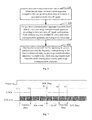
- FIG. 1 is an implementation environment involved with a controlling method for frequency synchronization.
- the implementation environment is set within an LCD TV 100 , where the LCD TV 100 includes at least one main drive control chip 110 , a plurality of column drive control chips 130 and a front-end motherboard chip 150 .
- the main drive control chip 110 transmits data with the column drive control chips 130 in a point-to-point communicative way.
- the main drive control chip 110 is configured to receive front-end data sent by the front-end motherboard chip 150 , lock its own operating frequency at the frequency corresponding to the front-end data, and send the front-end data to each column drive control chip 130 according to the locked operating frequency, where the front-end data could be transmitted to the main drive control chip 110 in the form of data packet.
- a column drive control chip 130 (D-IC, source drive IC) is configured to lock its own operating frequency at the operating frequency of the main drive control chip 110 , to receive the front-end data sent by the main drive control chip 110 according to the locked operating frequency and to drive the control panel of the LCD TV to display normally with the front-end data.
- the display panel of the LCD TV includes multiple columns of subpixels, for example, a 4K2K panel has 12,000 columns of subpixels, while the number of column output control channels included in each of the column drive control chips 130 is limited, and every column of output control channel is connected with every column of subpixels correspondingly, the number of columns of subpixel that could be controlled by each of the column drive control chips 130 is limited. That's why the point-to-point communication system constituted by the LCD TV will include a main drive control chip 110 and a plurality of column drive control chips 130 , where front-end data are transmitted between the main drive control chip 110 and the column drive control chips 130 simultaneously.
- FIG. 2A is a handshake flow chart of frequency synchronization in a point-to-point communication method according to the present disclosure. Referring now to FIG. 1 and FIG. 2A , the frequency synchronization process in the existing point-to-point communication method is described below with the LCD TV 100 as an example.
- the operating frequency of the main drive control chip 110 is its own inherent frequency F 2 , and it performs initial clock training on each column drive control chip 130 according to the operating frequency F 2 , i.e., it sends corresponding clock training data to each column drive control chip 130 according to the operating frequency F 2 (e.g., the clock training data corresponding to the column drive control chip D-IC 1 is D-IC 1 Training DATA).
- each column drive control chip 130 will be adjusted gradually from F 1 to the operating frequency F 2 of the main drive control chip 110 .
- the clock training of all the column drive control chip 130 is successful, i.e., the operating frequency of all the column drive control chip 130 is locked at the operating frequency F 2 of the main drive control chip 110 , and the frequency-lock pins corresponding to each column drive control chip 130 respectively output high-level signals (e.g., the frequency-lock pin corresponding to the column drive control chip D-IC 1 is LOCK 1 , and its corresponding output is a high-level signal).
- the main drive control chip 110 starts to transmit corresponding front-end data to each of the column drive control chips 130 according to the operating frequency F 2 (e.g., the front-end data corresponding to the column drive control chip D-IC 1 is D-IC 1 DATA), so that each of the column drive control chips 130 drives the display panel of the LCD-TV 100 to display normally according to the corresponding front-end data.
- the operating frequency F 2 e.g., the front-end data corresponding to the column drive control chip D-IC 1 is D-IC 1 DATA
- each of the column drive control chips 130 could enter into the locking process of operation frequency at the moment when the LCD TV 100 is started, and enter into operating state to complement subsequent task of driving the display. It should be noted that, in the initial clock training process, the clock training of each column drive control chip 130 is performed at the same time, as illustrated in FIG. 2A , so there is not such a problem that the operating stability of the LCD TV 100 is bad.
- each column drive control chip 130 detects that certain bits of the front-end data remain unchanged consecutively, for example, the third bit of every one of a certain number of packets corresponding to the front-end data is 0 or 1, it recognizes that the front-end data is abnormal and the operating frequency of the main drive control chip 110 is unstable, and then it initiates a clock training request to the main drive control chip 110 to start clock training again, which might cause the LCD TV 100 to perform clock training several times intermittently and worsen the operating stability of the LCD TV 100 .
- the operating frequency of the main drive control chip 110 is still unstable, for example, if the frequency corresponding to the front-end data received by the main drive control chip 110 is F 3 , then the main drive control chip 110 would adjust its operating frequency from F 2 to F 3 .
- each column drive control chip 130 will recognize the abnormality.
- the column drive control chip D-IC 1 recognizes abnormality and initiates a clock training request to the main drive control chip 110 . Since the other column drive control chips 130 do not recognize abnormality, clock training is performed only on the column drive control chip D-IC 1 at the moment of T 2 -T 3 , and the other column drive control chips 130 are in waiting process. At the same time, the frequency-lock pin LOCK 1 corresponding to the column drive control chip D-IC 1 would output a low-level signal while the outputs of the frequency-lock pins corresponding to other column drive control chips 130 remain the same.
- the clock training for the column drive control chip D-IC 1 succeeds, i.e., the operating frequency of the column drive control chip D-IC 1 locks at the operating frequency F 3 of the main drive control chip 110 , and the main drive control chip 110 transmits corresponding front-end D-IC 1 DATA to the column drive control chip D-IC 1 according to the operating frequency F 3 .
- the column drive control chip D-IC 2 recognizes abnormality and initiates a clock training request to the main drive control chip 110 . Since the other column drive control chips 130 do not recognize abnormality, clock training is performed only on the column drive control chip D-IC 2 at the moment of T 4 -T 5 , while the other column drive control chips 130 are in waiting process. At the same time, the frequency-lock pin LOCK 2 corresponding to the column drive control chip D-IC 2 would output a low-level signal, while the outputs of the frequency-lock pins corresponding to other column drive control chips 130 remain the same.
- the clock training of the column drive control chip D-IC 2 succeeds, i.e. the operating frequency of the column drive control chip D-IC 2 locks at the operating frequency F 3 of the main drive control chip 110 , the main drive control chip 110 would transmit corresponding front-end data D-IC 2 DATA to the column drive control chip D-IC 2 according to the operating frequency F 3 .
- the frequency-lock signal LOCK of the main drive control chip 110 is the AND result of the signals output by the frequency-lock pin corresponding to each of the column drive control chips 130 , when the LCD-TV is started, the frequency-lock signal LOCK of the main drive control chip 110 would become high or low continuously, as illustrated in FIG. 2B .
- the main drive control chip 110 sends the front-end data and when the frequency-lock signal LOCK is low (NG), the main drive control chip 110 stops transmitting the front-end data and transmits clock training data, as a result, each column drive control chip 130 receives the front-end data intermittently, and correspondingly the picture being displayed by the display panel flashes continuously.
- each of the column drive control chips 130 might recognize the abnormality, which would cause the picture displayed by the display panel to flash continuously and the LCD TV 100 to work abnormally. This process is the same as the described process when the LCD TV 100 is started, and would not be described herein any more.
- this controlling method for frequency synchronization may be executed by the main drive control chip 110 of the LCD TV 100 and the method could include the following steps.
- Step 210 when the main drive control chip 110 recognizes that its operating frequency is unstable, it generates a clock turn-off signal.
- the instability of operating frequency of the main drive control chip might happen at the moment when the LCD TV is started, or when the main drive control chip is externally interfered.
- the main drive control chip is usually powered on with its own imminent frequency as its operating frequency, and when the frequency corresponding to the front-end data it has received does not synchronize with the imminent frequency, it needs to change its operating frequency and synchronize the operating frequency with the frequency corresponding to the front-end data. Therefore, when having not received any front-end data, the operating frequency of the main drive control chip could be considered as unstable, i.e., at the moment when the LCD TV is started, the instability of the operating frequency of the main drive control chip could be judged by the recognition of received front-end data.
- the operating frequency of the main drive control chip usually could maintain stable in a pretty long time. Therefore, the instability of the operating frequency could be recognized by judging whether or not the operating frequency jitters when the LCD TV has been started. For example, it could be judged through the number of clock impulses corresponding to the operating frequency whether or not the operating frequency of the main drive control chip is stable.
- the clock turn-off signal is configured to represent that the operating frequency of the main drive control chip is unstable, therefore, once the main drive control chip recognizes that the operating frequency is unstable, it could generate a clock turn-off signal to perform subsequent clock training on each of the column drive control chips.
- the clock turn-off signal could be identified by a valid high impulse, and when it is recognized that the clock turn-off signal is a high impulse, it means the main drive control chip is about to perform clock training on each column drive control chip.
- Step 230 the main drive control chip 110 transmits fixed data to each of the column drive control chips according to the clock turn-off signal and receives clock training requests initiated by each of the column drive control chips according to the fixed data.
- the fixed data is configured to enable each column drive control chip to recognize that the operating frequency of the main drive control chip is unstable.
- each column drive control chip could receive the fixed data sent by the main drive control chip simultaneously.
- the fixed data could be all 0s or all 1s.
- the fixed data could be either pre-set or be obtained by extracting and processing the front-end data.
- each column drive control chip initiates a clock training request to the main drive control chip, so that the operating frequency of the main drive control chip could be locked through clock training.
- a threshold could be set, so that if the number of time that data which is 0 or 1 is received consecutively is larger than the threshold, each column drive control chip would initiate a clock training request to the main drive control chip; otherwise each column drive control chip would keep frequency synchronized, which increase the fault-tolerant rate of the point-to-point communication system.
- Step 250 when recognizing that the operating frequency synchronizes with the frequency corresponding to the front-end data, the main drive control chip 110 responds to the clock training requests and transmits clock training data to each of the column drive control chips.
- main drive control chip could perform no clock training on each column drive control chip temporarily, in order to avoid the situation that when waiting to receive the front-end data the operating frequency of the main drive control chip is unstable and clock training is performed on each column drive control chip again. Therefore, clock training could be performed after the main drive control chip has received the front-end data, in order to ensure that after the clock training has been succeeded, each column drive control chip could enter into operating state and transmit the front-end data.
- a response to the clock training request happens after the operating frequency of the main drive control chip synchronizes with the frequency corresponding to the front-end data.
- front-end frequency-lock signal to recognize whether or not the operating frequency of the main drive control chip synchronizes with the frequency corresponding to the front-end data.
- the front-end frequency-lock signal is configured to represent whether or not the operating frequency of the main drive control chip is locked at the frequency corresponding to the front-end data. For example, it indicates that the operating frequency of the main drive control chip synchronizes with the frequency corresponding to the front-end data if the front-end frequency-lock signal is a valid high impulse, on the contrary, it indicates that the two frequencies have not been synchronized if the front-end frequency-lock signal is an invalid low impulse.
- the front-end frequency-lock signal is different from the frequency-lock signal LOCK illustrated in FIG. 3 .
- the frequency-lock signal LOCK is configured to represent whether or not each column drive control chip has locked its operating frequency at the operating frequency of the main drive control chip.
- each column drive control chip could receive clock training data sent by the main drive control chip, complete clock training according to the clock training data, and lock its own operating frequency at the operating frequency of the main drive control chip, thus realizing frequency synchronization between each column drive control chip and the main drive control chip.
- a clock training-frequency lock mechanism is realized, that is, controlling frequency synchronization process of a point-to-point communication system to be performed only after a clock turn-off signal has been generated, which ensures that all the column drive control chips are able to initiate clock training requests at the same time, causes the main drive control chip to start performing clock training on each column drive control chip at the same time, and thus avoid the problem that the operating stability of the point-to-point communication system is bad because the operating frequency of the main drive control chip is unstable and it causes the point-to-point communication system to perform clock training intermittently.
- the abovementioned method could further include the following step:
- the main drive control chip 110 enters into a preset self-test mode when the frequency-lock signal is valid and the main drive control chip 110 has not received the front-end data.
- the self-test mode is configured to indicate that the operating frequency of the main drive control chip at the moment when the main drive control chip is powered up. In other words, the main drive control chip would enter into the preset self-test mode at the moment the main drive control chip is powered up, to facilitate subsequent clock training on every column drive control chip.
- the operating frequency of the main drive control chip is unstable at the moment when the main drive control chip is powered up through a valid frequency-lock signal and the failure to receive the front-end data, where a valid frequency-lock signal is configured to represent that each of the column drive control chips has locked its operating frequency at the operating frequency of the main drive control chip.
- the initial clock training performed by each of the column drive control chips would not result in a bad operating stability of the point-to-point communication system, and the main drive control chip would lock its own operating frequency at the frequency corresponding to the front-end data after having received the front-end data, therefore, at the moment of powering up, it would happen after the initial clocking training of each of the column drive control chips is successful and before the operating frequency of the main drive control chip synchronizes with the frequency corresponding to the front-end data that the operating frequency of the main drive control chip is unstable.
- the column drive control chip would correspondingly output a valid-level signal representing that the operating frequency has been successfully locked, for example, a high-level signal. Because the frequency-lock signal of the main drive control chip is the AND result of the signals output by each of the column drive control chips correspondingly, the frequency-lock signal of the main drive control chip would be marked as valid correspondingly.
- the operating frequency of the main drive control chip is unstable at the moment of powering up if the frequency-lock signal is valid and the front-end data is not received, causing the main drive control chip to enter into the self-test mode in preparation for performing clock training on each of the column drive control chips.
- step 210 could include the following operation:
- the main drive control chip 110 recognizes the received front-end data in the preset self-test mode and generates a clock turn-off signal through the recognized front-end data.
- the clock training could be performed after the main drive control chip has received the front-end data, in order to ensure that each of the column drive control chips could enter into operating state and transmit the front-end data once the clock training is successful, thus improving the efficiency of the clock training.
- the clock turn-off signal can be generated through recognition for received front-end data, for example, the front-end data is usually set with an initial identifier which represents that the front-end data has been sent, and thus the recognition is directed at the initial identifier of the front-end data.
- the initial identifier can be a valid high impulse signal, it indicates that the reception of the front-end data has been started when the initial identifier is recognized as valid high impulse.
- the main drive control chip After recognizing that the reception of the front-end data has been started, the main drive control chip determines that it could start to prepare for the clock training of each of the column drive control chips and correspondingly generates a clock turn-off signal, which is, for example, to raise the clock turn-off signal by one impulse and mark it with a valid high impulse.
- the abovementioned method could also include the following steps.
- Step 310 when being powered up, the main drive control chip 110 sends clock training data to each of the column drive control chips.
- Step 330 after each of the column drive control chips has completed clock training according to the clock training data, the main drive control chip 110 marks the frequency-lock signal as valid.
- the main drive control chip when being powered up, sends clock training data to each of the column drive control chips so that each of the column drive control chips could lock its operating frequency at the operating frequency of the main drive control chip.
- each of the column drive control chips performs clock training according to the clock training data, to lock its own operating frequency at the operating frequency of the main drive control chip, thus finishing the clock training.
- each of the column drive control chips would correspondingly output a valid-level signal configured to represent that its operating frequency has been locked successfully-for example, a high-level signal is used as a valid-level signal, and send it to the main drive control chip.
- the main drive control chip marks its own frequency-lock signal according to the AND result of the received signals output by each of the column drive control chips correspondingly, in order to indicate whether or not each of the column drive control chips has locked its operating frequency at the operating frequency of the main drive control chip. For example, if the AND result is 1, then the frequency-lock signal is marked as valid to represent that each of the column drive control chips has locked its operating frequency at the operating frequency of the main drive control chip, that is, all the column drive control chips' frequencies are synchronized.
- the abovementioned method could include the following step:
- the frequency-lock signal is marked as invalid.
- the instability of operating frequency of the main drive control chip could be recognized by judging whether or not the operating frequency has jittered.
- the column drive control chip will generate a clock impulse signal, in order to mark its own operating frequency with the number of clock impulses included in the clock impulse signal. For example, if the operating frequency is 100 MHZ, the number of clock impulses included in the clock impulse signal is 10 and if the operating frequency is 200 MHz, the number of clock impulses included in the clock impulse signal is 20.
- the preset range is 9-10, if the number of clock impulses is 12, it means that the column drive control chip fails to lock its operating frequency at the operating frequency of the main drive control chip, which is 100 MHz, and it recognizes that the operating frequency of the main drive control chip is unstable.
- the column drive control chip After having recognized that the number of clock impulses is not within a preset range, the column drive control chip will output an invalid-level signal (e.g., a low-level signal) to indicate that the lock of its operating frequency fails. Because the frequency-lock signal of the main drive control chip is the AND result of the signals output by each column drive control chip correspondingly, the frequency-lock signal of the main drive control chip is marked as invalid, to facilitate new clock training on the column drive control chips.
- an invalid-level signal e.g., a low-level signal
- the step 210 could include a following step:
- the main drive control chip 110 generates a clock turn-off signal according to the invalid frequency-lock signal.
- the main drive control chip After the main drive control chip marks the frequency-lock signal as invalid, the main drive control chip judges that its own operating frequency is unstable and it needs to perform clock training on each of the column drive control chips again, thus correspondingly generate a clock turn-off signal. For example, the main drive control chip raises the clock turn-off signal by one impulse and mark it with a valid high impulse.
- the operation of transmitting fixed data to each of the column drive control chips according to the clock turn-off signal could include the following steps.
- Step 231 the main drive control chip 110 extracts a preset bit from the front-end data according to the clock turn-off signal.
- the main drive control chip transmits the fixed-data.
- the fixed data is obtained by extracting process performed on the front-end data.
- the front-end data is represented by bit.
- the front-end data includes 32 bits.
- the extraction of the fixed data could be performed on a preset bit of the front-end data.
- the preset bit could be the highest bit of the front-end data (the 31 st bit) or the lowest bit (the 0 th bit), or another arbitrary bit of the front-end data (the 15 th bit).
- the fixed data also includes 32 bits and each of the bits is the preset bit.
- Step 233 the main drive control chip 110 uses the extracted preset bit as the fixed data and transmits the fixed data to each of the column drive control chips.
- the main drive control chip After extracting the preset bit, the main drive control chip sends the preset bit as the fixed data consecutively to each column drive control chip, so that each of the column drive control chips could recognize that the operating frequency of the main drive control chip is unstable.
- consecutive data (the fixed data consists of all 0s or all 1s) is transmitted consecutively, which avoids prolonging the start-up time of the main drive control chip, increases the fault-tolerant rate of the point-to-point communication system, and thus it would not happen that the clock training requests are not sent because the number of times that each of the column drive control chips recognizes consecutive data is too small, or that the clock training requests are sent by mistake because the number of times that each column drive control chip recognizes consecutive data is too big.
- the abovementioned method could also include the following step:
- the main drive control chip adjusts its operating frequency according to the frequency corresponding to the front-end data, so that the operating frequency could be locked at the frequency corresponding to the front-end data.
- the clock training requests is responded after the operating synchronization of the main drive control chip synchronizes with the frequency corresponding to the front-end data.
- the operating frequency of the main drive control chip would be adjusted so that the operating frequency is locked at the frequency corresponding to the front-end data.
- some embodiments provide a controlling method for frequency synchronization, applied in a point-to-point communication system, where the point-to-point communication system includes a pre-stage communication apparatus and a plurality of post-stage communication apparatuses, and the method could be executed by the pre-stage communication device, the method includes the following steps.
- Step 410 when the pre-stage communication apparatus recognizes that its operating frequency is unstable, it generates a clock turn-off signal.
- Step 430 the pre-stage communication apparatus transmits fixed data to each of the post-stage communication apparatuses according to the clock turn-off signal, and receives a clock training request initiated by each of the post-stage communication apparatuses according to the fixed data.
- Step 450 after having recognized that the operating frequency synchronizes with the frequency corresponding to the received front-end data, the pre-stage communication apparatus responds to the clock training request and transmits clock training data to each of the post-stage communication apparatuses.
- the process above could ensure that every post-stage communication device could initiate a clock training request to the pre-stage communication device and the pre-stage communication device could respond to the clock training requests at the same time, thus avoiding the point-to-point communication system performing clock training intermittently, and improving operating stability of the point-to-point communication system.
- FIG. 7 is a flow chart of the implementation of the controlling method for frequency synchronization in an application scenario.
- the point-to-point communication system is an LCD TV, where it includes a main drive control chip and a plurality of column drive control chips, and explain the flow chart of the implementation.
- the Power on signal is raised and when recognizing the rising edge of the Power on signal, at the moment of T 1 , the main drive control chip transmits Training Data (clock training data) to each of the column drive control chips at its own operating frequency (the imminent frequency), to perform initial clock training on each of the column drive control chips and have the operating frequency of each of the column drive control chips locked at the imminent frequency of the main drive control chip.
- Training Data clock training data
- each of the column drive control chips has been successful in its clock training, and the frequency-lock signal LOCK of the main drive control chip is raised. Because the front-end data (SOC data) sent by the front-end motherboard chip has not been received yet, the main drive control chip will transmit data to each of the column drive control chips at its own operating frequency and enter into the preset self-test mode (Bist mode).
- the main drive control chip In the Bist mode, at the moment of T 3 , when the main drive control chip has received the SOC data, it generates the clock turn-off signal (Clk off signal), and transmits the fixed data to each of the column drive control chips at the current operating frequency according to the Clk off signal to obtain the clock training request initiated by each of the column drive control chips according to the fixed data and lowers the frequency-lock signal LOCK.
- the clock turn-off signal (Clk off signal)
- the main drive control chip When the operating frequency of the main drive control chip is locked at the frequency corresponding to the SOC Data, it means that the operating frequency of the main drive control chip is stable, which is at the moment of T 4 , then the main drive control chip responds to the clock training request and transmits the training data to each of the column drive control chips.
- Each column drive control chip performs the clock training according to the training data, and locks its operating frequency at the operating frequency of the main drive control chip at the moment of T 5 , where the operating frequency of the main drive control chip at the moment of T 5 is the frequency corresponding to the SOC Data, and the frequency-lock signal LOCK is raised again.
- each of the column drive control chips enters into operating states, receives the SOC Data at its own operating frequency and drives the LCD TV's display panel to display normally according to the SOC data.
- the abovementioned process ensures that each of the column drive control chips could initiate a clock training request to the main drive control chip at the same time, and the main drive control chip could respond to the clock training requests at the same time, avoiding that the picture displayed in the display panel of the LCD TV is displayed abnormally from time to time, thus improving the displaying stability of the LCD TV.
- some embodiments provide a controlling device 700 for frequency synchronization, applied to a LCD TV, where the LCD TV includes a front-end motherboard chip, a main drive control chip and a plurality of column drive control chips are integrated within.
- the device 700 includes but is not limited to: a turn-off signal generating unit 710 , a fixed-data transmitting unit 730 and a training request responding unit 750 .
- the turn-off signal generating unit 710 is configured to generate a clock turn-off signal when recognizing that the operating frequency of main drive control chip is unstable.
- the fixed-data transmitting unit 730 is configured to transmit fixed data to each of the column drive control chips according to the clock turn-off signal and receive clock a training request initiated by each of the column drive control chips according to the fixed data.
- the training request responding unit 750 is configured to respond to the clock training requests and transmit clock training data to each of the column drive control chips after having recognized that the operating frequency of the main drive control chip synchronizes with the frequency corresponding to front-end data transmitted by the front-end motherboard chip.
- the abovementioned device 700 includes but is not limited to: a self-test entering unit.
- the self-test entering unit is configured to control the main drive control chip to enter a preset self-test mode when the frequency-lock signal is valid and the front-end data has not been received.
- each of the column drive control chips has locked its operating frequency at the frequency of the main drive control chip if the frequency-lock signal is valid, and the number of clock impulses is configured to mark the operating frequency.
- the turn-off signal generating unit 710 includes but is not limited to: a front-end data recognition module.
- the front-end data recognition module recognizes the front-end data received by the main drive control chip in the preset self-test mode and generate a clock turn-off signal according to the recognized front-end data.
- the abovementioned device 700 further includes but is not limited to: a training data transmitting unit 810 and a lock signal validity marking unit 830 .
- the training data transmission unit 810 is configured to transmit the clock training data to each of the column drive control chips at the time of powering up.
- the lock signal validity marking unit 830 is configured to mark the frequency-lock signal as valid after each of the column drive control chips has finished the clock training according to the clock training data.
- the device 700 further includes but is not limited to: a lock signal invalidity marking unit.
- the lock signal invalidity marking unit is configured to mark the frequency lock signal as invalid when the number of clock impulses included in the clock impulse signals generated by each of the column drive control chips is not within the preset range.
- the turn-off signal generating unit 710 includes but is not limited to: a generation module.
- the generation module is configured to generate a clock turn-off signal according to an invalid frequency-lock signal.
- the fixed-data transmitting unit 730 includes but is not limited to: an extraction module 731 and a transmission module 733 .
- the extraction module 731 is configured to perform preset bit extraction on the front-end data according to the clock turn-off signal.
- the transmission module 733 is configured to transmit the extracted preset bit as the fixed data to each of the column drive control chips.
- the abovementioned device 700 includes but is not limited to: a frequency adjusting unit.
- the frequency adjusting unit is configured to adjust the operating frequency of the main drive control chip according to the frequency corresponding to the front-end data, so that the operating frequency of the main drive control chip could be locked at the frequency corresponding to the front-end data.
- the frequency synchronization process of the controlling device for frequency synchronization is exemplified only by the division of the above-described functional modules.
- the above-described functions may be assigned to different functional modules to be completed as needed, that is, the internal structure of the controlling device for frequency synchronization will be divided into different functional modules to complete all or part of the functions described above.
- Some embodiments provide another controlling device 800 for frequency synchronization.
- the device 800 is applied to an LCD TV, where the LCD TV includes a front-end motherboard chip, a main drive control chip and a plurality of column drive control chips.
- the device 800 includes at least one processor 810 and a memory 820 .
- the processor 810 can be the main drive control chip, in other words, the main drive control chip is common to the LCD TV and the device 800 .
- the memory 820 stores therein instructions executable by the at least one processor 810 , and the instructions are executed by the at least one processor to enable the at least one processor to:
- the at least one processor 810 is further configured to:
- the at least one process 810 is configured to generate a clock turn-off signal by the following operation:
- the at least one processor 810 is further configured to perform the following operations:
- the at least one processor 810 is further configured to:
- the at least one processor 810 is configured to generate a clock turn-off signal by:
- the at least one processor 810 is configured to transmit fixed data to each column drive control chip according to the clock turn-off signal by the following operations:
- the at least one processor is further configured to:
- the operating frequency of the main drive control chip when recognizing that the operating frequency of the main drive control chip synchronizes with the frequency corresponding to the front-end data sent by the front-end motherboard chip, before the operation of transmitting clock training data to each column drive control chip in response to the clock training request, adjust the operating frequency of the main drive control chip according to the frequency corresponding to the front-end data, so that the operating frequency of the main drive control chip is locked at the frequency corresponding to the front-end data.
- the at least one processor 810 recognizes that operating frequency of the main drive control chip is unstable, by:
- the at least one processor 810 recognizes that the operating frequency of the main drive control chip is unstable.
- the at least one processor 810 recognizes that operating frequency of the main drive control chip is unstable, by:
- the at least one processor 810 determines that the operating frequency of the main drive control chip jitters, the at least one processor 810 recognizes that the operating frequency of the main drive control chip is unstable.
- the at least one processor 810 determines that the operating frequency of the main drive control chip jitters, by:
- the at least one processor 810 determines that the number of clock impulses corresponding to the operating frequency of the main drive control chip changes, determining that the operating frequency of the main drive control chip jitters.
- some embodiments provides another controlling device 900 for frequency synchronization, applied to a point-to-point system, where the point-to-point communication system includes a pre-stage communication apparatus and a plurality of post-stage communication apparatuses, the device 900 including: at least one processor 910 and a memory 920 .
- the processor 910 can be the main drive control chip, in other words, the main drive control chip is common to the LCD TV and the device 900 .
- the memory 920 stores therein instructions executable by the at least one processor 910 , and the instructions are executed by the at least one processor 910 to enable the at least one processor 910 to:
- the controlling device for frequency synchronization and the controlling method for frequency synchronization according to the abovementioned embodiments belong to the same conception, and the specific mode in which each module performs the operations has been described in detail in the method embodiments, which would not be described here again.
Landscapes
- Engineering & Computer Science (AREA)
- Chemical & Material Sciences (AREA)
- Crystallography & Structural Chemistry (AREA)
- Physics & Mathematics (AREA)
- Computer Hardware Design (AREA)
- General Physics & Mathematics (AREA)
- Theoretical Computer Science (AREA)
- Control Of Indicators Other Than Cathode Ray Tubes (AREA)
- Multimedia (AREA)
- Signal Processing (AREA)
Abstract
Description
Claims (17)
Priority Applications (1)
| Application Number | Priority Date | Filing Date | Title |
|---|---|---|---|
| US15/858,064 US10152932B2 (en) | 2016-09-20 | 2017-12-29 | Controlling device and method for frequency synchronization and LCD television |
Applications Claiming Priority (3)
| Application Number | Priority Date | Filing Date | Title |
|---|---|---|---|
| CN201610834444.4 | 2016-09-20 | ||
| CN201610834444 | 2016-09-20 | ||
| CN201610834444.4A CN106412379B (en) | 2016-09-20 | 2016-09-20 | Control method, device and LCD TV for realizing frequency synchronization |
Related Child Applications (1)
| Application Number | Title | Priority Date | Filing Date |
|---|---|---|---|
| US15/858,064 Continuation US10152932B2 (en) | 2016-09-20 | 2017-12-29 | Controlling device and method for frequency synchronization and LCD television |
Publications (2)
| Publication Number | Publication Date |
|---|---|
| US20170201656A1 US20170201656A1 (en) | 2017-07-13 |
| US9892698B2 true US9892698B2 (en) | 2018-02-13 |
Family
ID=57997002
Family Applications (2)
| Application Number | Title | Priority Date | Filing Date |
|---|---|---|---|
| US15/471,912 Active US9892698B2 (en) | 2016-09-20 | 2017-03-28 | Controlling device and method for frequency synchronization and LCD television |
| US15/858,064 Active US10152932B2 (en) | 2016-09-20 | 2017-12-29 | Controlling device and method for frequency synchronization and LCD television |
Family Applications After (1)
| Application Number | Title | Priority Date | Filing Date |
|---|---|---|---|
| US15/858,064 Active US10152932B2 (en) | 2016-09-20 | 2017-12-29 | Controlling device and method for frequency synchronization and LCD television |
Country Status (2)
| Country | Link |
|---|---|
| US (2) | US9892698B2 (en) |
| CN (1) | CN106412379B (en) |
Families Citing this family (4)
| Publication number | Priority date | Publication date | Assignee | Title |
|---|---|---|---|---|
| KR102418971B1 (en) * | 2017-11-15 | 2022-07-11 | 삼성디스플레이 주식회사 | Display device and driving method thereof |
| CN108693465A (en) * | 2018-03-30 | 2018-10-23 | 北京联想核芯科技有限公司 | A kind of test control method, circuit and system |
| US10848160B2 (en) * | 2018-07-10 | 2020-11-24 | Aerotech, Inc. | Devices, systems, and methods for reducing jitter in control systems |
| CN109410881B (en) * | 2018-12-20 | 2020-06-02 | 深圳市华星光电技术有限公司 | Signal transmission system and signal transmission method |
Citations (9)
| Publication number | Priority date | Publication date | Assignee | Title |
|---|---|---|---|---|
| US6654065B1 (en) * | 1999-08-31 | 2003-11-25 | Lg Electronics Inc. | Apparatus for generating timing and synchronizing signals for a digital display device |
| US6972803B2 (en) * | 2003-09-10 | 2005-12-06 | Gennum Corporation | Video signal format detector and generator system and method |
| US6985141B2 (en) * | 2001-07-10 | 2006-01-10 | Canon Kabushiki Kaisha | Display driving method and display apparatus utilizing the same |
| US7256836B2 (en) * | 2000-06-23 | 2007-08-14 | Kabushiki Kaisha Toshiba | Image processing system and method, and image display system |
| US7411633B2 (en) * | 2004-06-30 | 2008-08-12 | Canon Kabushiki Kaisha | Display apparatus and method for controlling the same |
| US7859594B2 (en) * | 2005-11-11 | 2010-12-28 | Sony Corporation | Display driving signal processor, display apparatus and a method of processing display driving signal |
| US8294820B2 (en) * | 2008-08-20 | 2012-10-23 | Kabushiki Kaisha Toshiba | Video signal synchronization signal generating apparatus and video signal synchronization signal generation method |
| US8502899B2 (en) * | 2008-06-06 | 2013-08-06 | Sony Corporation | Solid-state imaging device, imaging device, electronic equipment, A/D converter and A/D conversion method |
| US8582033B2 (en) * | 2009-05-22 | 2013-11-12 | Megachips Corporation | Movie reproduction system and movie reproduction method for reducing delay time of reproduced movie |
Family Cites Families (6)
| Publication number | Priority date | Publication date | Assignee | Title |
|---|---|---|---|---|
| JP3120200B2 (en) * | 1992-10-12 | 2000-12-25 | セイコーインスツルメンツ株式会社 | Light valve device, stereoscopic image display device, and image projector |
| JP4649706B2 (en) * | 2000-06-08 | 2011-03-16 | ソニー株式会社 | Display device and portable terminal using the same |
| US7830348B2 (en) * | 2003-12-11 | 2010-11-09 | Au Optronics Corporation | Integrated circuit for liquid crystal display device |
| TWI270032B (en) * | 2004-06-14 | 2007-01-01 | Au Optronics Corp | Liquid crystal display device |
| US7420874B2 (en) * | 2005-04-06 | 2008-09-02 | Rambus Inc. | Integrated circuit memory device, system and method having interleaved row and column control |
| CN204993623U (en) * | 2015-06-10 | 2016-01-20 | 广州创维平面显示科技有限公司 | TV set and backlight time schedule control circuit thereof |
-
2016
- 2016-09-20 CN CN201610834444.4A patent/CN106412379B/en active Active
-
2017
- 2017-03-28 US US15/471,912 patent/US9892698B2/en active Active
- 2017-12-29 US US15/858,064 patent/US10152932B2/en active Active
Patent Citations (9)
| Publication number | Priority date | Publication date | Assignee | Title |
|---|---|---|---|---|
| US6654065B1 (en) * | 1999-08-31 | 2003-11-25 | Lg Electronics Inc. | Apparatus for generating timing and synchronizing signals for a digital display device |
| US7256836B2 (en) * | 2000-06-23 | 2007-08-14 | Kabushiki Kaisha Toshiba | Image processing system and method, and image display system |
| US6985141B2 (en) * | 2001-07-10 | 2006-01-10 | Canon Kabushiki Kaisha | Display driving method and display apparatus utilizing the same |
| US6972803B2 (en) * | 2003-09-10 | 2005-12-06 | Gennum Corporation | Video signal format detector and generator system and method |
| US7411633B2 (en) * | 2004-06-30 | 2008-08-12 | Canon Kabushiki Kaisha | Display apparatus and method for controlling the same |
| US7859594B2 (en) * | 2005-11-11 | 2010-12-28 | Sony Corporation | Display driving signal processor, display apparatus and a method of processing display driving signal |
| US8502899B2 (en) * | 2008-06-06 | 2013-08-06 | Sony Corporation | Solid-state imaging device, imaging device, electronic equipment, A/D converter and A/D conversion method |
| US8294820B2 (en) * | 2008-08-20 | 2012-10-23 | Kabushiki Kaisha Toshiba | Video signal synchronization signal generating apparatus and video signal synchronization signal generation method |
| US8582033B2 (en) * | 2009-05-22 | 2013-11-12 | Megachips Corporation | Movie reproduction system and movie reproduction method for reducing delay time of reproduced movie |
Also Published As
| Publication number | Publication date |
|---|---|
| CN106412379A (en) | 2017-02-15 |
| US10152932B2 (en) | 2018-12-11 |
| US20180122316A1 (en) | 2018-05-03 |
| US20170201656A1 (en) | 2017-07-13 |
| CN106412379B (en) | 2019-02-15 |
Similar Documents
| Publication | Publication Date | Title |
|---|---|---|
| US10152932B2 (en) | Controlling device and method for frequency synchronization and LCD television | |
| CN106023910B (en) | Signal transmitting and receiving system and time schedule controller of related display | |
| AU2021266341B2 (en) | Session processing method, device, and system | |
| US9755818B2 (en) | Method to enhance MIPI D-PHY link rate with minimal PHY changes and no protocol changes | |
| US20150220472A1 (en) | Increasing throughput on multi-wire and multi-lane interfaces | |
| CN107769906B (en) | Semiconductor device, data transmission system, and method for operating semiconductor device | |
| TWI649966B (en) | Low voltage differential signaling transmitter and low voltage differential signaling receiver | |
| EP3637396B1 (en) | Drive control method, assembly and display apparatus | |
| CN109818610B (en) | Clock data recovery circuit and method, and apparatus including clock data recovery circuit | |
| US20170041086A1 (en) | Data transmission apparatus for changing clock signal at runtime and data interface system including the same | |
| EP3637397A1 (en) | Drive control method, assembly and display apparatus | |
| KR20200004026A (en) | Clock recovery device and source driver for recovering embedded clock from interface signal | |
| KR20210081608A (en) | Touch sensing device for display device including | |
| KR20160145901A (en) | Display device and control method of the same | |
| US20160118010A1 (en) | Display Driving Apparatus, Source Driver and Skew Adjustment Method | |
| US12488728B2 (en) | Image data transmission device and method, electronic apparatus, medium, and display system | |
| US9792193B2 (en) | Method and system for processing data conflict | |
| KR20200005971A (en) | Clock recovery device and source driver for recovering embedded clock from interface signal | |
| US9865205B2 (en) | Method for transmitting data from timing controller to source driver and associated timing controller and display system | |
| CN105989789B (en) | Method for transmitting data from time schedule controller, time schedule controller and display system | |
| EP4383622A1 (en) | Feedback method, related device, and readable storage medium | |
| CN117527530A (en) | VBO communication method, VBO interface and display terminal | |
| CN117975866A (en) | Display device | |
| JP6773868B1 (en) | Transmitter, transmission method and program | |
| CN109862206A (en) | Method for transmitting signals |
Legal Events
| Date | Code | Title | Description |
|---|---|---|---|
| AS | Assignment |
Owner name: HISENSE ELECTRIC CO., LTD., CHINA Free format text: ASSIGNMENT OF ASSIGNORS INTEREST;ASSIGNORS:ZHANG, SHILI;FANG, HAOQIANG;TIAN, QINGHUA;AND OTHERS;REEL/FRAME:041770/0674 Effective date: 20170111 |
|
| AS | Assignment |
Owner name: HISENSE USA CORPORATION, GEORGIA Free format text: ASSIGNMENT OF AN UNDIVIDED INTEREST;ASSIGNOR:HISENSE ELECTRIC CO., LTD.;REEL/FRAME:042441/0297 Effective date: 20170407 Owner name: HISENSE INTERNATIONAL CO., LTD., CHINA Free format text: ASSIGNMENT OF AN UNDIVIDED INTEREST;ASSIGNOR:HISENSE ELECTRIC CO., LTD.;REEL/FRAME:042441/0297 Effective date: 20170407 |
|
| STCF | Information on status: patent grant |
Free format text: PATENTED CASE |
|
| MAFP | Maintenance fee payment |
Free format text: PAYMENT OF MAINTENANCE FEE, 4TH YEAR, LARGE ENTITY (ORIGINAL EVENT CODE: M1551); ENTITY STATUS OF PATENT OWNER: LARGE ENTITY Year of fee payment: 4 |
|
| MAFP | Maintenance fee payment |
Free format text: PAYMENT OF MAINTENANCE FEE, 8TH YEAR, LARGE ENTITY (ORIGINAL EVENT CODE: M1552); ENTITY STATUS OF PATENT OWNER: LARGE ENTITY Year of fee payment: 8 |