US9872349B2 - Control system for phase-cut dimming - Google Patents
Control system for phase-cut dimming Download PDFInfo
- Publication number
- US9872349B2 US9872349B2 US14/937,179 US201514937179A US9872349B2 US 9872349 B2 US9872349 B2 US 9872349B2 US 201514937179 A US201514937179 A US 201514937179A US 9872349 B2 US9872349 B2 US 9872349B2
- Authority
- US
- United States
- Prior art keywords
- power transmission
- feedback signal
- phase
- signal
- transmission circuit
- Prior art date
- Legal status (The legal status is an assumption and is not a legal conclusion. Google has not performed a legal analysis and makes no representation as to the accuracy of the status listed.)
- Active
Links
Images


Classifications
-
- H05B33/0818—
-
- H05B33/0812—
-
- H05B33/0845—
-
- H—ELECTRICITY
- H05—ELECTRIC TECHNIQUES NOT OTHERWISE PROVIDED FOR
- H05B—ELECTRIC HEATING; ELECTRIC LIGHT SOURCES NOT OTHERWISE PROVIDED FOR; CIRCUIT ARRANGEMENTS FOR ELECTRIC LIGHT SOURCES, IN GENERAL
- H05B45/00—Circuit arrangements for operating light-emitting diodes [LED]
- H05B45/10—Controlling the intensity of the light
-
- H—ELECTRICITY
- H05—ELECTRIC TECHNIQUES NOT OTHERWISE PROVIDED FOR
- H05B—ELECTRIC HEATING; ELECTRIC LIGHT SOURCES NOT OTHERWISE PROVIDED FOR; CIRCUIT ARRANGEMENTS FOR ELECTRIC LIGHT SOURCES, IN GENERAL
- H05B45/00—Circuit arrangements for operating light-emitting diodes [LED]
- H05B45/30—Driver circuits
- H05B45/37—Converter circuits
- H05B45/3725—Switched mode power supply [SMPS]
- H05B45/385—Switched mode power supply [SMPS] using flyback topology
-
- H—ELECTRICITY
- H05—ELECTRIC TECHNIQUES NOT OTHERWISE PROVIDED FOR
- H05B—ELECTRIC HEATING; ELECTRIC LIGHT SOURCES NOT OTHERWISE PROVIDED FOR; CIRCUIT ARRANGEMENTS FOR ELECTRIC LIGHT SOURCES, IN GENERAL
- H05B45/00—Circuit arrangements for operating light-emitting diodes [LED]
- H05B45/30—Driver circuits
- H05B45/395—Linear regulators
-
- H05B33/0809—
-
- H05B33/0815—
-
- H05B33/0824—
-
- H05B33/0851—
-
- H—ELECTRICITY
- H05—ELECTRIC TECHNIQUES NOT OTHERWISE PROVIDED FOR
- H05B—ELECTRIC HEATING; ELECTRIC LIGHT SOURCES NOT OTHERWISE PROVIDED FOR; CIRCUIT ARRANGEMENTS FOR ELECTRIC LIGHT SOURCES, IN GENERAL
- H05B45/00—Circuit arrangements for operating light-emitting diodes [LED]
- H05B45/40—Details of LED load circuits
- H05B45/44—Details of LED load circuits with an active control inside an LED matrix
-
- Y—GENERAL TAGGING OF NEW TECHNOLOGICAL DEVELOPMENTS; GENERAL TAGGING OF CROSS-SECTIONAL TECHNOLOGIES SPANNING OVER SEVERAL SECTIONS OF THE IPC; TECHNICAL SUBJECTS COVERED BY FORMER USPC CROSS-REFERENCE ART COLLECTIONS [XRACs] AND DIGESTS
- Y02—TECHNOLOGIES OR APPLICATIONS FOR MITIGATION OR ADAPTATION AGAINST CLIMATE CHANGE
- Y02B—CLIMATE CHANGE MITIGATION TECHNOLOGIES RELATED TO BUILDINGS, e.g. HOUSING, HOUSE APPLIANCES OR RELATED END-USER APPLICATIONS
- Y02B20/00—Energy efficient lighting technologies, e.g. halogen lamps or gas discharge lamps
- Y02B20/30—Semiconductor lamps, e.g. solid state lamps [SSL] light emitting diodes [LED] or organic LED [OLED]
-
- Y02B20/343—
Definitions
- Embodiments relate to a control system for phase-cut dimming.
- a phase of the AC can be passed as much as a dimming angle.
- a system for controlling power supplied to a load of the power transmission circuit is needed.
- Embodiments are directed to providing a control system of phase-cut dimming through embodiments.
- phase-cut dimming control system including a phase angle detector configured to detect a phase angle of an input voltage generated by phase-cut dimming, a feedback signal generator configured to generate a first reference signal corresponding to the detected phase angle, and generate an initial feedback signal based on a detection signal corresponding to power supplied to a load and the first reference signal, a feedback signal modulator configured to modulate the initial feedback signal and generate a feedback signal, a power transmission controller configured to generate a control signal which controls power transmission according to the feedback signal, and a power transmission circuit configured to transmit power to the load according to the control signal.
- the feedback signal modulator may include a hysteresis filter to output the feedback signal based on a hysteresis level corresponding to a variation of the initial feedback signal among a plurality of hysteresis levels.
- the power transmission controller may include an input current controller to control an amount of an input current that flows into the power transmission circuit according to the feedback signal.
- the power transmission circuit may control a duty according to the control signal. Further, the power transmission circuit may control the amount of the input current according to a reference signal based on the control signal.
- the power transmission controller may include a powering operation controller to control a time during which power is transmitted from the power transmission circuit to the load according to the feedback signal.
- the powering operation controller may detect the power transmission time by counting time. Further, the powering operation controller may control the power transmission circuit to transmit power during a period in which the input voltage is at a level equal to or more than a predetermined level determined according to the feedback signal.
- the power transmission circuit may perform a switching operation during an enabled period according to the control signal.
- the power transmission circuit may control the input current during an enabled period of a reference signal based on the control signal, and the input current may not be generated during a disabled period of the reference signal in the power transmission circuit.
- phase-cut dimming control system including a linear regulator configured to control a current that flows in at least one LED, and a power transmission controller configured to receive a feedback current that flows in the at least one LED, and to control the linear regulator to control an amount of an input current supplied to the at least one LED or a period in which the input current flows.
- the phase-cut dimming control system may further include a feedback signal generator configured to generate a feedback signal according to the current which flows in the at least one LED.
- the phase-cut dimming control system may further include a feedback signal modulator configured to modulate the feedback signal.
- the feedback signal generator may generate the feedback signal using a difference between a reference signal and a signal corresponding to the current which flows in the at least one LED, and the reference signal may be based on a phase angle of an input voltage supplied to the at least one LED.
- the feedback signal generator may generate the feedback signal which uniformly regulates the current which flows in the at least one LED when the detected phase angle is a predetermined threshold value or more.
- the power transmission controller may generate a control signal according to the feedback signal, and the linear regulator may control the amount of the input current according to a reference signal based on the control signal.
- the linear regulator may control the input current according to a reference signal during an enabled period of the reference signal based on the control signal.
- the input current may not be generated during a disabled period of the reference signal.
- the power transmission controller may determine a period, in which an input voltage supplied to the at least one LED is at a level equal to or more than a predetermined level determined according to the feedback signal, as the enabled period of the reference signal.
- Still another aspect of the invention provides a phase-cut dimming control system including a linear regulator configured to control a current which flows in at least one LED, an input voltage detector configured to generate a first control signal based on a result in which an input voltage supplied to the at least one LED is detected, and a power transmission controller configured to control the linear regulator according to the first control signal and control an amount of an input current supplied to the at least one LED or a period in which the input current flows.
- Yet another aspect of the invention provides a phase-cut dimming control system including a linear regulator configured to control a current which flows in at least one LED, and a power transmission controller configured to control the linear regulator according to a preset control signal and control an amount of an input current supplied to the at least one LED or a period in which the input current flows.
- a control system for phase-cut dimming is provided through the embodiments.
- FIG. 1 is a view illustrating an application example of a control system for phase-cut dimming according to one embodiment.
- FIG. 2 is a block diagram illustrating each configuration of one embodiment.
- FIG. 3 is a view illustrating a waveform of an input voltage.
- FIG. 4A is a view illustrating one example of a relationship between a phase angle signal and a reference signal.
- FIG. 4B is a view illustrating another example of a relationship between a phase angle signal and a reference signal.
- FIG. 4C is a view illustrating still another example of a relationship between a phase angle signal and a reference signal.
- FIG. 5 is a waveform diagram for describing an operation of a hysteresis filter according to one embodiment.
- FIG. 6A is a view illustrating a low-pass filter implemented with an analog filter according to one embodiment.
- FIG. 6B is a view illustrating a low-pass filter implemented with a digital filter according to one embodiment.
- FIG. 7A is a waveform diagram illustrating an input current control according to one embodiment.
- FIG. 7B is a waveform diagram illustrating a power time control according to one embodiment.
- FIG. 8 is a view illustrating one example of a power transmission circuit according to one embodiment.
- FIG. 9 is a view illustrating another example of a power transmission circuit according to one embodiment.
- FIG. 10 is an application example of a phase-cut dimming control system according to another embodiment.
- FIG. 11 is an application example of a phase-cut dimming control system according to still another embodiment.
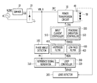
- FIG. 1 is a view illustrating an application example of a control system for phase-cut dimming according to one embodiment.
- an alternating current (AC) is supplied to a power transmission circuit 30 through a dimmer 10 and a rectifier circuit 20 .
- Power is supplied from the power transmission circuit 30 to a load 50 .
- the power supplied to the load 50 may be detected by a sensor 40 and the detection result may be transmitted to a load detector 200 .
- the dimmer 10 blocks phases other than those within the dimming angle among phases of a line voltage VLINE.
- a voltage VIN phase-cut by the dimmer 10 is rectified through the rectifier circuit 20 , and an input voltage VIN_R is generated.
- Such an input voltage VIN_R, on which phase-cut dimming is performed, is transmitted to the power transmission circuit 30 .
- the rectifier circuit 20 generates the input voltage VIN_R by full-wave rectifying the voltage VIN with a full-wave rectifier circuit.
- the power transmission circuit 30 supplies the power to the load 50 using the input voltage VIN_R.
- a phase angle detector 100 generates a phase angle signal PA based on a phase angle ratio with respect to one half cycle of the line voltage VLINE.
- the phase angle refers to a dimming angle of the dimmer 10 . Since the one half cycle of the line voltage VLINE is the same as one cycle of the input voltage VIN_R, the phase angle detector 100 may generate the phase angle signal PA based on a phase angle ratio with respect to the one cycle of the input voltage VIN_R.
- FIG. 3 is a view illustrating a waveform of an input voltage.
- the phase angle detector 100 detects a period PT 2 in which the input voltage VIN_R is generated for one cycle (PT 1 +PT 2 ) of the input voltage VIN_R.
- the phase angle detector 100 may generate a phase angle signal PA based on a value (PT 2 /(PT 1 +PT 2 )) calculated by dividing the period PT 2 by the cycle (PT 1 +PT 2 ).
- the load detector 200 may detect the load 50 using the output of the sensor 40 .
- the sensor 40 may have a configuration capable of detecting a current supplied to the load 50 .
- the invention is not limited thereto, and the load detector 200 may indirectly detect the power supplied to the load 50 . Since a detailed method thereof is clearly understood through the art to which the invention pertains to easily carry out, a detailed description thereof will be omitted.
- the load detector 200 generates a signal SENSE detected according to the detection result of the power supplied to the load 50 .
- the load detector 200 may directly receive information on a current detected by the sensor 40 .
- the load detector 200 may indirectly detect the current, which flows in the load 50 , through an opto-coupler.
- a feedback signal generator 300 generates a reference signal based on the phase angle signal PA, and an initial feedback signal FBIN is generated using a difference between the signal SENSE detected from the load detector 200 and the reference signal.
- a feedback signal modulator 400 modulates the initial feedback signal FBIN to generate a feedback signal FBMOD.
- the feedback signal modulator 400 may generate the feedback signal FBMOD by filtering noise components of the initial feedback signal FBIN.
- a power transmission controller 500 generates a control signal CTRL for a power transmission control according to the feedback signal FBMOD, and the control signal CTRL may be transmitted to the power transmission circuit 30 .
- FIG. 2 is a block diagram illustrating each configuration of one embodiment.
- a load 50 may include at least one light emitting diode (LED), and the load 50 is implemented with three LEDs connected in series in FIG. 2 . Furthermore, a load detector 200 detects a current, which flows in the load 50 , through a sensor 40 in FIG. 2 .
- LED light emitting diode
- a feedback signal generator 300 includes a reference signal generator 310 and a loop controller 320 .
- a reference signal generator 310 generates a reference signal REF based on a phase angle signal PA.
- FIG. 4A is a view illustrating one example of a relationship between a phase angle signal and a reference signal.
- the reference signal generator 310 may generate a reference signal REF in proportion to a phase angle signal PA.
- FIG. 4B is a view illustrating another example of a relationship between a phase angle signal and a reference signal.
- the reference signal generator 310 may generate a reference signal REF in proportion to a phase angle signal PA in a region in which the phase angle signal PA is smaller than a predetermined threshold value PTH 1 , and may generate a reference signal REF at a constant level VREF 1 in a region in which the phase angle signal PA is the threshold value PTH 1 or more.
- FIG. 4C is a view illustrating still another example of a relationship between a phase angle signal and a reference signal.
- the reference signal generator 310 may generate a reference signal REF at a constant level VREF 2 or VREF 3 in respective regions in which a phase angle signal PA is smaller than a predetermined first threshold value PTH 2 and is a predetermined second threshold value PTH 3 or more, and may generate a reference signal REF having a predetermined slope in proportion to the phase angle signal PA in a region between the first threshold value PTH 2 and the second threshold value PTH 3 .
- the feedback signal generator 300 may generate an initial feedback signal FBIN to uniformly regulate the current which flows in the load 50 .
- Proportional slopes of the phase angle signal PA and the reference signal REF shown in FIGS. 4A and 4B and a proportional slope shown in FIG. 4C are different from each other.
- a loop controller 320 generates the initial feedback signal FBIN using the reference signal REF and the detected signal SENSE transmitted from the load detector 200 .
- the loop controller 320 may amplify a difference between a voltage of the detected signal SENSE and a voltage of the reference signal REF, and may generate the initial feedback signal FBIN.
- a feedback signal modulator 400 may include at least one of a hysteresis filter 410 and a low-pass filter 420 to remove a noise of the initial feedback signal FBIN.
- the hysteresis filter 410 outputs a hysteresis level corresponding to a variation of the initial feedback signal FBIN among a plurality of hysteresis levels as a feedback signal FBMOD.
- FIG. 5 is a waveform diagram for describing an operation of a hysteresis filter according to one embodiment.
- an initial feedback signal FBIN is shown as a dashed line, and a feedback signal FBMOD is shown as a solid line.
- the initial feedback signal FBIN shown in FIG. 5 is shown as a waveform which ascends and descends, and then is changeable in a predetermined range, but the invention is not limited thereto.
- the feedback signal FBMOD ascends from a hysteresis level HYS 1 to the hysteresis level HYS 2 .
- the feedback signal FBMOD ascends from the hysteresis level HYS 2 to the hysteresis level HYS 3
- the feedback signal FBMOD ascends from the hysteresis level HYS 3 to the hysteresis level HYS 4 .
- the feedback signal FBMOD descends from the hysteresis level HYS 4 to the hysteresis level HYS 3 .
- the feedback signal FBMOD descends from the hysteresis level HYS 3 to the hysteresis level HYS 2 .
- the feedback signal FBMOD is maintained at the hysteresis level HYS 2 .
- the low-pass filter 420 performs low-pass filtering on the initial feedback signal FBIN to generate the feedback signal FBMOD.
- the low-pass filter 420 may be implemented as an analog filter or digital filter.
- FIG. 6A is a view illustrating a low-pass filter implemented with an analog filter according to one embodiment.
- a low-pass filter 420 includes a resistor R 1 and a capacitor C 1 .
- the initial feedback signal FBIN is input to one end of the resistor R 1 , and the capacitor C 1 is connected to the other end of the resistor R 1 .
- a voltage at a point of contact between the resistor R 1 and the capacitor C 1 becomes a feedback signal FBMOD.
- FIG. 6B is a view illustrating a low-pass filter implemented with a digital filter according to one embodiment.
- a low-pass filter 420 includes a first register 421 , a second register 422 , an adder 423 , and a divider 424 .
- An initial feedback signal FBIN is sampled by a predetermined cycle, then an initial feedback signal FNIN[n ⁇ 2] sampled prior to a second cycle is stored in the second register 422 , and an initial feedback signal FNIN[n ⁇ 1] sampled prior to a first cycle is stored in the first register 421 .
- the adder 423 adds a currently sampled initial feedback signal FNIN[n], the initial feedback signal FNIN[n ⁇ 1] sampled prior to the first cycle, and the initial feedback signal FNIN[n ⁇ 2] sampled prior to the second cycle, and the divider 424 calculates an average by dividing the output of the adder 423 by three. The calculated result becomes a feedback signal FBMOD.
- a power transmission controller 500 may include at least one of an input current controller 510 and a powering operation controller 520 to control power transmission according to the feedback signal FBMOD.
- the input current controller 510 generates a control signal CTRL which controls an intensity of an input current according to the feedback signal FBMOD.
- the input current INP is a current which flows into the power transmission circuit 30 .
- the powering operation controller 520 controls a time during which power is transmitted from the power transmission circuit 30 to the load 50 according to the feedback signal FBMOD.
- the powering operation controller 520 may detect a power transmission time determined according to the feedback signal FBMOD by counting elapsed time.
- the powering operation controller 520 may set a period, which is equal to or more than a specific level in which the input voltage VIN_R is determined according to the feedback signal FBMOD, to the power transmission time.
- a switching device of the power transmission circuit 30 may operate or the current which flows in the load 50 may be controlled at a predetermined level, during the power transmission time.
- a feedback signal FBMOD is shown gradationally decreasing, but this is an assumption to explain the input current control according to the feedback signal FBMOD only, and the invention is not limited thereto.
- An input voltage VIN_R has a waveform in which full-wave rectification is performed on a voltage VIN passed through the dimmer 10 .
- the input voltage VIN_R ascends at time T 1 and an input current INP flows into the power transmission circuit 30 .
- the input voltage VIN_R becomes zero-voltage at time T 2 , and the input voltage VIN_R is not generated and the input current INP does not flow during a period from time T 2 to time T 3 .
- An amount of the input current INP is determined according to a control signal CTRL during a period from time T 1 to time T 2 .
- the input current controller 510 may generate the control signal CTRL which controls a duty of the power transmission circuit 30 according to the feedback signal FBMOD, or may generate the control signal CTRL as a reference signal which controls the amount of the input current INP.
- the input current controller 510 When the feedback signal FBMOD descends at time T 2 , the input current controller 510 generates a control signal CTRL to reduce the amount of the input current INP according to the descent of the feedback signal FBMOD. For example, the input current controller 510 may generate the control signal CTRL by which a duty decreases compared to the period from time T 1 to time T 2 , or may generate the control signal CTRL as a reference signal by which the amount of the input current INP decreases compared to the period from time T 1 to time T 2 .
- the input voltage VIN_R ascends at time T 3 and the input current INP starts to flow into the power transmission circuit 30 .
- the input voltage VIN_R becomes zero-voltage at time T 4 , and the input voltage VIN_R is not generated and the input current INP does not flow during a period from time T 4 to time T 5 .
- the amount of the input current INP during a period from time T 3 to time T 4 is smaller than the amount of the input current INP during the period from time T 1 to time T 2 .
- the input voltage VIN_R ascends at time T 5 and the input current INP starts to flow into the power transmission circuit 30 .
- the input voltage VIN_R becomes zero-voltage at time T 6 , and the input voltage VIN_R is not generated and the input current INP does not flow after passing time T 6 .
- the amount of the input current INP during a period from time T 5 to time T 6 is smaller than the amount of the input current INP during the period from time T 3 to time T 4 .
- a feedback signal FBMOD is shown gradationally decreasing, but this is an assumption for describing the power time control according to the feedback signal FBMOD only, and the invention is not limited thereto.
- An input voltage VIN_R ascends at time T 11 and an input current INP starts to flow into the power transmission circuit 30 .
- the input current INP flows during a period from time T 11 to time T 12 , the input voltage VIN_R becomes zero-voltage at time T 13 , and the input voltage VIN_R is not generated and the input current INP does not flow during a period from time T 13 to time T 14 .
- the period from time T 11 to time T 12 , in which the input current INP flows within one cycle of the input voltage VIN_R, is determined according to a control signal CTRL.
- the powering operation controller 520 generates the control signal CTRL to control a power transmission time, i.e., a period in which the input current INP flows, according to the feedback signal FBMOD.
- the powering operation controller 520 may generate a control signal CTRL which controls an enabled period of a reference signal which controls the amount of the input current INP.
- the reference signal has a predetermined level during the enabled period only, and may be not generated during a disabled period.
- the powering operation controller 520 transmits a control signal CTRL having a predetermined level as the reference signal during the period from time T 11 to time T 12 to the power transmission circuit 30 , and the power transmission circuit 30 controls the input current INP according to the control signal CTRL during the period from time T 11 to time T 12 .
- the control signal CTRL may not be generated and the input current INP may also not be generated during a disabled period from time T 12 to time T 13 .
- the powering operation controller 520 When the feedback signal FBMOD descends at time T 13 , the powering operation controller 520 generates a control signal CTRL to reduce a power transmission time according to the descent of the feedback signal FBMOD.
- the powering operation controller 520 may generate the control signal CTRL which enables the switching operation of the power transmission circuit 30 during a period from time T 14 to time T 15 which is short compared to the period from time T 11 to time T 12 .
- the powering operation controller 520 may generate the control signal CTRL as a reference signal during the period from time T 14 to time T 15 which is short compared to the period from time T 11 to time T 12 .
- a period from time T 15 to time T 16 is a disabled period of the reference signal and the control signal CTRL may not be generated.
- the powering operation controller 520 When the feedback signal FBMOD descends at time T 16 , the powering operation controller 520 generates a control signal CTRL to reduce a power transmission time according to the descent of the feedback signal FBMOD.
- the powering operation controller 520 may generate the control signal CTRL which enables the switching operation of the power transmission circuit 30 during a period from time T 17 to time T 18 which is short compared to the period from time T 14 to time T 15 .
- the powering operation controller 520 may generate the control signal CTRL as a reference signal during the period from time T 17 to time T 18 which is short compared to the period from time T 14 to time T 15 .
- a period from time T 18 to time T 19 is a disabled period of the reference signal and the control signal CTRL may not be generated.
- the input current INP which is input to a next cycle of the input voltage VIN_R (not shown), may flow into the power transmission circuit 30 during a period the same as the period from time T 17 to time T 18 .
- the power transmission circuit 30 may be implemented by various methods.
- FIG. 8 is a view illustrating one example of a power transmission circuit according to one embodiment.
- a power transmission circuit 30 may be implemented as a switch mode power supply.
- the power transmission circuit 30 includes a first winding W 1 connected to an input voltage VIN_R, a second winding W 2 connected to a load 50 , a power switch 32 , a duty generator 31 , a rectifier diode D 1 , a capacitor C 2 , and a resistor R 2 .
- the duty generator 31 controls a switching operation of the power switch 32 by a duty according to a control signal CTRL. For example, when an amount of an input current INP is controlled according to the control signal CTRL, the duty generator 31 may control the switching operation of the power switch 32 by the duty according to the control signal CTRL. When a power transmission time is controlled according to the control signal CTRL, the duty generator 31 may control the switching operation of the power switch 32 by a predetermined duty, and may enable or disable the switching operation according to the control signal CTRL.
- FIG. 9 is a view illustrating another example of a power transmission circuit according to one embodiment.
- a power transmission circuit 30 includes a transistor 34 , a linear regulator 33 , and a resistor R 3 .
- a drain of the transistor 34 is connected to a load 50 , the resistor R 3 is connected between a source of the transistor 34 and a ground, an output terminal of the linear regulator 33 is connected to a gate of the transistor 34 .
- the linear regulator 33 may be implemented as an operational amplifier, and when a control signal CTRL is input to a non-inverting terminal (+) of the linear regulator 33 , an amount of an input current INP or a power transmission time may be controlled.
- a voltage of the resistor R 3 is input to an inverting terminal ( ⁇ ) of the linear regulator 33 , and the output of the linear regulator 33 is determined according to a difference between the input of the inverting terminal ( ⁇ ) and the input of the non-inverting terminal (+).
- a current, which flows in the transistor 34 is controlled according to the output of the linear regulator 33 so as to control the input of the inverting terminal ( ⁇ ) and the input of the non-inverting terminal (+) to be identical. That is, the current, which flows in the load 50 , is controlled according to the control signal CTRL, and thus the input current INP is controlled.
- the current, which flows in the transistor 34 is controlled to have an amount based on the control signal CTRL.
- the power transmission time is controlled according to the control signal CTRL, the current, which flows in the transistor 34 , flows with the amount based on the control signal CTRL during an enabled period of the control signal CTRL which is a reference signal, and a current does not flow in the transistor 34 during a disabled period of the control signal CTRL.
- a loop control system for controlling power supplied to a load of a power system, to which phase-cut dimming is applied through the embodiment, is provided.
- an operation of a power transmission circuit may be controlled by an open loop method.
- FIG. 10 is an application example of a phase-cut dimming control system according to another embodiment.
- a load 50 shown in FIG. 10 includes at least one LED.
- the embodiment shown in FIG. 10 does not detect a current supplied to the load 50 , detects information on an input voltage VIN_R, and a first control signal CTRL 1 is generated according to the detection result.
- an input voltage detector 600 may generate the first control signal CTRL 1 by detecting at least one of a phase angle of the input voltage VIN_R (PT 2 /(PT 1 +PT 2 )) (see FIG. 3 ), a period PT 1 or period PT 2 of the input voltage VIN_R, a peak or average of the input voltage VIN_R, and a level of the input voltage VIN_R.
- the peak of the input voltage VIN_R refers to a peak within a one-cycle period, and refers to a one-cycle average of the input voltage VIN_R.
- the meaning of the detection of the level of the input voltage VIN_R refers to a determination whether the input voltage VIN_R is a predetermined threshold voltage or more.
- the input voltage detector 600 includes a phase angle detector 610 and a level detector 620 in FIG. 10 , the invention is not limited thereto.
- the phase angle detector 610 may detect the input voltage VIN_R to detect the phase angle of the input voltage VIN_R, and may generate a first control signal CTRL according to the detected phase angle. For example, the phase angle detector 610 detects the phase angle using a method the same as that of the phase angle detector 100 described with reference to FIG. 3 , and the first control signal CTRL 1 is generated according to the detected phase angle.
- the level detector 620 may detect the level of the input voltage VIN_R, and may generate a first control signal CTRL according to the detected level. For example, the level detector 620 compares the input voltage VIN_R with the predetermined threshold voltage, and the first control signal CTRL 1 , which is enabled during a period in which the input voltage VIN_R is the threshold voltage or more, may be generated.
- the input current controller 710 generates a second control signal CTRL 2 which controls an amount of the input current according to the first control signal CTRL 1 .
- the power transmission circuit 30 controls the amount of the input current according to the second control signal CTRL 2 using a method the same as that previously described with reference to FIG. 7A .
- the power transmission circuit 30 may control the switching operation of the power switch 32 using a duty depending on the second control signal CTRL 2 .
- the second control signal CTRL 2 may be a reference signal supplied to the non-inverting terminal (+) of the linear regulator 33 .
- the powering operation controller 720 generates the second control signal CTRL 2 which controls a power transmission time according to the first control signal CTRL 1 .
- the power transmission circuit 30 controls the power transmission time according to the second control signal CTRL 2 using a method the same as that previously described with reference to FIG. 7B .
- the power transmission circuit 30 may enable or disable the switching operation of the power switch 32 according to the second control signal CTRL 2 .
- the second control signal CTRL 2 is supplied to the non-inverting terminal (+) of the linear regulator 33 .
- a current flows in the transistor 33 by the output of the linear regulator 33 during an enabled period in which the second control signal CTRL 2 is at a predetermined level.
- the transistor 33 turns off by the output of the linear regulator 33 and a current does not flow in the transistor 33 during a disabled period in which the second control signal CTRL 2 is at a ground level.
- a current may be supplied to a load according to a predetermined control signal without considering the input voltage.
- FIG. 11 is an application example of a phase-cut dimming control system according to still another embodiment.
- a load 50 shown in FIG. 11 includes at least one LED.
- a powering operation controller 800 may receive the input of a control signal CTRLC having a constant level, and may generate a third control signal CTRL 3 which controls a power transmission circuit 30 to transmit power during a period depending on the control signal CTRLC.
- the power transmission circuit 30 may enable or disable a switching operation of the power switch 32 according to the third control signal CTRL 2 .
- the third control signal CTRL 3 is supplied to the non-inverting terminal (+) of the linear regulator 33 .
- a current flows in the transistor 33 by the output of the linear regulator 33 during an enabled period in which the third control signal CTRL 3 is at a predetermined level.
- the transistor 33 turns off by the output of the linear regulator 33 and a current does not flow in the transistor 33 during a disabled period in which the third control signal CTRL 3 is at a ground level.
Landscapes
- Circuit Arrangement For Electric Light Sources In General (AREA)
- Physics & Mathematics (AREA)
- General Physics & Mathematics (AREA)
- Dc-Dc Converters (AREA)
Abstract
Description
Claims (10)
Priority Applications (2)
| Application Number | Priority Date | Filing Date | Title |
|---|---|---|---|
| US14/937,179 US9872349B2 (en) | 2014-11-10 | 2015-11-10 | Control system for phase-cut dimming |
| US15/835,119 US10412798B2 (en) | 2014-11-10 | 2017-12-07 | Control system for phase-cut dimming |
Applications Claiming Priority (2)
| Application Number | Priority Date | Filing Date | Title |
|---|---|---|---|
| US201462077394P | 2014-11-10 | 2014-11-10 | |
| US14/937,179 US9872349B2 (en) | 2014-11-10 | 2015-11-10 | Control system for phase-cut dimming |
Related Child Applications (1)
| Application Number | Title | Priority Date | Filing Date |
|---|---|---|---|
| US15/835,119 Division US10412798B2 (en) | 2014-11-10 | 2017-12-07 | Control system for phase-cut dimming |
Publications (2)
| Publication Number | Publication Date |
|---|---|
| US20160135265A1 US20160135265A1 (en) | 2016-05-12 |
| US9872349B2 true US9872349B2 (en) | 2018-01-16 |
Family
ID=55913368
Family Applications (2)
| Application Number | Title | Priority Date | Filing Date |
|---|---|---|---|
| US14/937,179 Active US9872349B2 (en) | 2014-11-10 | 2015-11-10 | Control system for phase-cut dimming |
| US15/835,119 Active 2035-12-16 US10412798B2 (en) | 2014-11-10 | 2017-12-07 | Control system for phase-cut dimming |
Family Applications After (1)
| Application Number | Title | Priority Date | Filing Date |
|---|---|---|---|
| US15/835,119 Active 2035-12-16 US10412798B2 (en) | 2014-11-10 | 2017-12-07 | Control system for phase-cut dimming |
Country Status (2)
| Country | Link |
|---|---|
| US (2) | US9872349B2 (en) |
| KR (1) | KR20160055696A (en) |
Cited By (5)
| Publication number | Priority date | Publication date | Assignee | Title |
|---|---|---|---|---|
| US10292236B2 (en) * | 2015-06-18 | 2019-05-14 | Shenzhen Sendis Semiconductor Co., Ltd | Linear constant current LED drive device capable of driving reduced number of LEDs |
| US10306724B2 (en) | 2017-01-15 | 2019-05-28 | Ecosense Lighting Inc. | Lighting systems, and systems for determining periodic values of a phase angle of a waveform power input |
| US10483850B1 (en) | 2017-09-18 | 2019-11-19 | Ecosense Lighting Inc. | Universal input-voltage-compatible switched-mode power supply |
| US11051386B2 (en) | 2018-09-06 | 2021-06-29 | Lsi Industries, Inc. | Distributed intelligent network-based lighting system |
| US20250380344A1 (en) * | 2022-06-24 | 2025-12-11 | Hangzhou Tuya Information Technology Co., Ltd. | Driving circuit and method compatible with scr and wireless dimming, lamp, and system |
Families Citing this family (5)
| Publication number | Priority date | Publication date | Assignee | Title |
|---|---|---|---|---|
| US9307588B2 (en) | 2012-12-17 | 2016-04-05 | Ecosense Lighting Inc. | Systems and methods for dimming of a light source |
| JP6551735B2 (en) * | 2015-06-09 | 2019-07-31 | パナソニックIpマネジメント株式会社 | Dimmable lighting circuit and lighting fixture |
| EP3504941A4 (en) * | 2016-08-26 | 2020-01-15 | Ozuno Holdings Limited | SIGNALING PROCEDURE FOR LOAD CONTROLLING DIMMER |
| WO2020117382A1 (en) * | 2018-12-07 | 2020-06-11 | Hubbell Incorporated | Automatic trimming for a dimmer switch |
| US11543995B2 (en) | 2021-03-22 | 2023-01-03 | Micron Technology, Inc. | Feedback for multi-level signaling in a memory device |
Citations (10)
| Publication number | Priority date | Publication date | Assignee | Title |
|---|---|---|---|---|
| US7295452B1 (en) * | 2006-09-07 | 2007-11-13 | Green Mark Technology Inc. | Active power factor correction circuit and control method thereof |
| US7667408B2 (en) | 2007-03-12 | 2010-02-23 | Cirrus Logic, Inc. | Lighting system with lighting dimmer output mapping |
| US7759881B1 (en) * | 2008-03-31 | 2010-07-20 | Cirrus Logic, Inc. | LED lighting system with a multiple mode current control dimming strategy |
| US20110074302A1 (en) * | 2009-09-30 | 2011-03-31 | Draper William A | Phase Control Dimming Compatible Lighting Systems |
| US20110266967A1 (en) * | 2010-04-30 | 2011-11-03 | Osram Gesellschaft Mit Beschraenkter Haftung | Method and system for driving led |
| US8558477B2 (en) * | 2010-04-30 | 2013-10-15 | Osram Gesellschaft Mit Beschraenkter Haftung | Method and device for obtaining conduction angle, method and device for driving LED |
| US8558518B2 (en) * | 2008-03-25 | 2013-10-15 | Microsemi Corporation | Methods and apparatuses for phase-cut dimming at low conduction angles |
| US8890425B2 (en) * | 2012-03-09 | 2014-11-18 | Silergy Semiconductor Technology (Hangzhou) Ltd | Blend dimming circuits and relevant methods |
| US9131581B1 (en) * | 2014-03-14 | 2015-09-08 | Lightel Technologies, Inc. | Solid-state lighting control with dimmability and color temperature tunability |
| US20150359052A1 (en) * | 2014-06-06 | 2015-12-10 | Nxp B.V. | Switched mode power supply |
Family Cites Families (6)
| Publication number | Priority date | Publication date | Assignee | Title |
|---|---|---|---|---|
| US8729870B2 (en) * | 2008-08-15 | 2014-05-20 | Analog Modules, Inc. | Biphase laser diode driver and method |
| US8466628B2 (en) * | 2009-10-07 | 2013-06-18 | Lutron Electronics Co., Inc. | Closed-loop load control circuit having a wide output range |
| US9942954B2 (en) * | 2010-05-14 | 2018-04-10 | Lumastream Canada Ulc | Method and system for controlling solid state lighting via dithering |
| US8680787B2 (en) * | 2011-03-15 | 2014-03-25 | Lutron Electronics Co., Inc. | Load control device for a light-emitting diode light source |
| US9066381B2 (en) * | 2011-03-16 | 2015-06-23 | Integrated Illumination Systems, Inc. | System and method for low level dimming |
| US20130229215A1 (en) * | 2012-03-02 | 2013-09-05 | Laurence P. Sadwick | Variable Resistance for Driver Circuit Dithering |
-
2015
- 2015-11-04 KR KR1020150154687A patent/KR20160055696A/en not_active Ceased
- 2015-11-10 US US14/937,179 patent/US9872349B2/en active Active
-
2017
- 2017-12-07 US US15/835,119 patent/US10412798B2/en active Active
Patent Citations (10)
| Publication number | Priority date | Publication date | Assignee | Title |
|---|---|---|---|---|
| US7295452B1 (en) * | 2006-09-07 | 2007-11-13 | Green Mark Technology Inc. | Active power factor correction circuit and control method thereof |
| US7667408B2 (en) | 2007-03-12 | 2010-02-23 | Cirrus Logic, Inc. | Lighting system with lighting dimmer output mapping |
| US8558518B2 (en) * | 2008-03-25 | 2013-10-15 | Microsemi Corporation | Methods and apparatuses for phase-cut dimming at low conduction angles |
| US7759881B1 (en) * | 2008-03-31 | 2010-07-20 | Cirrus Logic, Inc. | LED lighting system with a multiple mode current control dimming strategy |
| US20110074302A1 (en) * | 2009-09-30 | 2011-03-31 | Draper William A | Phase Control Dimming Compatible Lighting Systems |
| US20110266967A1 (en) * | 2010-04-30 | 2011-11-03 | Osram Gesellschaft Mit Beschraenkter Haftung | Method and system for driving led |
| US8558477B2 (en) * | 2010-04-30 | 2013-10-15 | Osram Gesellschaft Mit Beschraenkter Haftung | Method and device for obtaining conduction angle, method and device for driving LED |
| US8890425B2 (en) * | 2012-03-09 | 2014-11-18 | Silergy Semiconductor Technology (Hangzhou) Ltd | Blend dimming circuits and relevant methods |
| US9131581B1 (en) * | 2014-03-14 | 2015-09-08 | Lightel Technologies, Inc. | Solid-state lighting control with dimmability and color temperature tunability |
| US20150359052A1 (en) * | 2014-06-06 | 2015-12-10 | Nxp B.V. | Switched mode power supply |
Cited By (5)
| Publication number | Priority date | Publication date | Assignee | Title |
|---|---|---|---|---|
| US10292236B2 (en) * | 2015-06-18 | 2019-05-14 | Shenzhen Sendis Semiconductor Co., Ltd | Linear constant current LED drive device capable of driving reduced number of LEDs |
| US10306724B2 (en) | 2017-01-15 | 2019-05-28 | Ecosense Lighting Inc. | Lighting systems, and systems for determining periodic values of a phase angle of a waveform power input |
| US10483850B1 (en) | 2017-09-18 | 2019-11-19 | Ecosense Lighting Inc. | Universal input-voltage-compatible switched-mode power supply |
| US11051386B2 (en) | 2018-09-06 | 2021-06-29 | Lsi Industries, Inc. | Distributed intelligent network-based lighting system |
| US20250380344A1 (en) * | 2022-06-24 | 2025-12-11 | Hangzhou Tuya Information Technology Co., Ltd. | Driving circuit and method compatible with scr and wireless dimming, lamp, and system |
Also Published As
| Publication number | Publication date |
|---|---|
| US20160135265A1 (en) | 2016-05-12 |
| US10412798B2 (en) | 2019-09-10 |
| US20180098398A1 (en) | 2018-04-05 |
| KR20160055696A (en) | 2016-05-18 |
Similar Documents
| Publication | Publication Date | Title |
|---|---|---|
| US9872349B2 (en) | Control system for phase-cut dimming | |
| CN104206023B (en) | Circuit and method for driving light-emitting diode (LED) | |
| US8456108B2 (en) | LED lighting apparatus | |
| US9520794B2 (en) | Acceleration of output energy provision for a load during start-up of a switching power converter | |
| US8736194B2 (en) | LED dimmer circuit | |
| US10412796B2 (en) | LED drive circuit with a programmable input for LED lighting | |
| TWI527494B (en) | Driving circuits, methods and controllers for driving light source | |
| US9119254B2 (en) | Light emitting device power supply circuit with dimming function and control circuit thereof | |
| US10015851B2 (en) | Ballast circuit | |
| CN102907173B (en) | With with the LED manipulation portion of the constant-current source of clock signal duty | |
| US9167662B2 (en) | Mixed load current compensation for LED lighting | |
| RU2677625C2 (en) | Systems and methods for valley switching in pulsed power converter | |
| KR101698948B1 (en) | Light-emitting diode lighting device having multiple driving stages and line/load regulation control | |
| JP2013223389A (en) | Power supply system | |
| US8674615B2 (en) | Control apparatus for LED diodes | |
| KR101142106B1 (en) | Group dimmable constant current led converter | |
| EP2973969B1 (en) | Quantization error reduction in constant output current control drivers | |
| US20190350056A1 (en) | System and method for shaping input current in light emitting diode (led) system | |
| KR101705831B1 (en) | Apparatus for dimming light emmiting devices | |
| KR20110011536A (en) | Dimmer for ac light emitting device | |
| KR20160122544A (en) | LED driving apparatus controling brightness based on resistance | |
| JP5810306B2 (en) | LED lighting device and lighting apparatus using the same | |
| KR20130142910A (en) | Dimming angle sensing circuit, dimming angle sensing method, and power supply device comprising the dimming angle sensing circuit |
Legal Events
| Date | Code | Title | Description |
|---|---|---|---|
| AS | Assignment |
Owner name: FAIRCHILD KOREA SEMICONDUCTOR LTD., KOREA, REPUBLI Free format text: ASSIGNMENT OF ASSIGNORS INTEREST;ASSIGNORS:EUM, HYUNCHUL;KIM, YOUNGJONG;HUANG, KUO-HSIEN;AND OTHERS;REEL/FRAME:037083/0743 Effective date: 20151109 |
|
| AS | Assignment |
Owner name: SEMICONDUCTOR COMPONENTS INDUSTRIES, LLC, ARIZONA Free format text: ASSIGNMENT OF ASSIGNORS INTEREST;ASSIGNOR:FAIRCHILD KOREA SEMICONDUCTOR, LTD.;REEL/FRAME:044361/0205 Effective date: 20171102 |
|
| AS | Assignment |
Owner name: DEUTSCHE BANK AG NEW YORK BRANCH, AS COLLATERAL AGENT, NEW YORK Free format text: PATENT SECURITY AGREEMENT;ASSIGNORS:SEMICONDUCTOR COMPONENTS INDUSTRIES, LLC;FAIRCHILD SEMICONDUCTOR CORPORATION;REEL/FRAME:044481/0541 Effective date: 20170504 Owner name: DEUTSCHE BANK AG NEW YORK BRANCH, AS COLLATERAL AG Free format text: PATENT SECURITY AGREEMENT;ASSIGNORS:SEMICONDUCTOR COMPONENTS INDUSTRIES, LLC;FAIRCHILD SEMICONDUCTOR CORPORATION;REEL/FRAME:044481/0541 Effective date: 20170504 |
|
| STCF | Information on status: patent grant |
Free format text: PATENTED CASE |
|
| MAFP | Maintenance fee payment |
Free format text: PAYMENT OF MAINTENANCE FEE, 4TH YEAR, LARGE ENTITY (ORIGINAL EVENT CODE: M1551); ENTITY STATUS OF PATENT OWNER: LARGE ENTITY Year of fee payment: 4 |
|
| AS | Assignment |
Owner name: FAIRCHILD SEMICONDUCTOR CORPORATION, ARIZONA Free format text: RELEASE OF SECURITY INTEREST IN PATENTS RECORDED AT REEL 04481, FRAME 0541;ASSIGNOR:DEUTSCHE BANK AG NEW YORK BRANCH, AS COLLATERAL AGENT;REEL/FRAME:064072/0459 Effective date: 20230622 Owner name: SEMICONDUCTOR COMPONENTS INDUSTRIES, LLC, ARIZONA Free format text: RELEASE OF SECURITY INTEREST IN PATENTS RECORDED AT REEL 04481, FRAME 0541;ASSIGNOR:DEUTSCHE BANK AG NEW YORK BRANCH, AS COLLATERAL AGENT;REEL/FRAME:064072/0459 Effective date: 20230622 |
|
| MAFP | Maintenance fee payment |
Free format text: PAYMENT OF MAINTENANCE FEE, 8TH YEAR, LARGE ENTITY (ORIGINAL EVENT CODE: M1552); ENTITY STATUS OF PATENT OWNER: LARGE ENTITY Year of fee payment: 8 |