US9859862B2 - Gain peaking techniques in high-frequency passive low pass filters - Google Patents
Gain peaking techniques in high-frequency passive low pass filters Download PDFInfo
- Publication number
- US9859862B2 US9859862B2 US14/471,213 US201414471213A US9859862B2 US 9859862 B2 US9859862 B2 US 9859862B2 US 201414471213 A US201414471213 A US 201414471213A US 9859862 B2 US9859862 B2 US 9859862B2
- Authority
- US
- United States
- Prior art keywords
- low pass
- pass filter
- chip
- passive low
- circuit
- Prior art date
- Legal status (The legal status is an assumption and is not a legal conclusion. Google has not performed a legal analysis and makes no representation as to the accuracy of the status listed.)
- Expired - Fee Related, expires
Links
Images


Classifications
-
- H—ELECTRICITY
- H03—ELECTRONIC CIRCUITRY
- H03H—IMPEDANCE NETWORKS, e.g. RESONANT CIRCUITS; RESONATORS
- H03H7/00—Multiple-port networks comprising only passive electrical elements as network components
- H03H7/01—Frequency selective two-port networks
- H03H7/0153—Electrical filters; Controlling thereof
-
- H—ELECTRICITY
- H03—ELECTRONIC CIRCUITRY
- H03H—IMPEDANCE NETWORKS, e.g. RESONANT CIRCUITS; RESONATORS
- H03H11/00—Networks using active elements
- H03H11/02—Multiple-port networks
- H03H11/04—Frequency selective two-port networks
- H03H11/12—Frequency selective two-port networks using amplifiers with feedback
- H03H11/1204—Distributed RC filters
-
- H—ELECTRICITY
- H03—ELECTRONIC CIRCUITRY
- H03H—IMPEDANCE NETWORKS, e.g. RESONANT CIRCUITS; RESONATORS
- H03H7/00—Multiple-port networks comprising only passive electrical elements as network components
- H03H7/38—Impedance-matching networks
- H03H7/40—Automatic matching of load impedance to source impedance
-
- H—ELECTRICITY
- H04—ELECTRIC COMMUNICATION TECHNIQUE
- H04B—TRANSMISSION
- H04B1/00—Details of transmission systems, not covered by a single one of groups H04B3/00 - H04B13/00; Details of transmission systems not characterised by the medium used for transmission
- H04B1/02—Transmitters
- H04B1/04—Circuits
- H04B1/0458—Arrangements for matching and coupling between power amplifier and antenna or between amplifying stages
-
- H—ELECTRICITY
- H04—ELECTRIC COMMUNICATION TECHNIQUE
- H04B—TRANSMISSION
- H04B1/00—Details of transmission systems, not covered by a single one of groups H04B3/00 - H04B13/00; Details of transmission systems not characterised by the medium used for transmission
- H04B1/06—Receivers
- H04B1/16—Circuits
- H04B1/18—Input circuits, e.g. for coupling to an antenna or a transmission line
-
- H—ELECTRICITY
- H03—ELECTRONIC CIRCUITRY
- H03H—IMPEDANCE NETWORKS, e.g. RESONANT CIRCUITS; RESONATORS
- H03H2210/00—Indexing scheme relating to details of tunable filters
- H03H2210/02—Variable filter component
- H03H2210/021—Amplifier, e.g. transconductance amplifier
-
- H—ELECTRICITY
- H03—ELECTRONIC CIRCUITRY
- H03H—IMPEDANCE NETWORKS, e.g. RESONANT CIRCUITS; RESONATORS
- H03H7/00—Multiple-port networks comprising only passive electrical elements as network components
- H03H7/38—Impedance-matching networks
- H03H7/383—Impedance-matching networks comprising distributed impedance elements together with lumped impedance elements
Definitions
- the disclosed technologies relate generally to wireless radio communications, and more particularly, to techniques for gain peaking in the frequency response of high-frequency passive low pass filters.
- the frequency response of passive low pass filters used in transmit and receive chains of wireless communications devices often have a slope in the passband signal.
- the drop in the passband signal at the cutoff frequency (Fc) can be pronounced.
- the drop in the passband signal is caused by the low-Q and the self-resonant frequency (SRF) of the on-chip spiral inductors of the passive low pass filter.
- SRF self-resonant frequency
- the drop in the frequency response of the passband signal caused by the filter can be between 3 and 5 dB at the cutoff frequency (Fc).
- the mixer and baseband amplifiers in the chain can also have a slope in the passband signal.
- the frequency response of the entire chain may have too much slope in the passband signal for a baseband chip or a radio frequency integrated circuit (RFIC) chip to work with.
- RFIC radio frequency integrated circuit
- FIG. 1 is a circuit diagram of an example passive low pass filter.
- FIG. 2 is a circuit diagram of an example passive low pass filter with the input and the output impedance of the filter mismatched to peak or increase the gain of the passband signal at the cutoff frequency of the filter, according to an embodiment of the present invention.
- FIG. 3 is a chart of the frequency response of the passive low pass filter of FIG. 2 .
- FIG. 4 is a circuit diagram example of a high-speed buffer driving a load through a transmission line on a printed circuit board.
- FIG. 5 is a diagram of the example circuit of FIG. 4 with the introduction of a passive low pass filter to peak or increase the gain of the passband signal at the cutoff frequency of the filter, according to an embodiment of the present invention.
- FIG. 6 is a chart of the frequency response of the high-speed printed circuit board interconnection of the example circuit of FIG. 4 and the frequency response of the interconnection with the introduction of an inductor stage in the form of a passive low pass filter between the driving chip and the loading chip as shown in the example circuit of FIG. 5 .
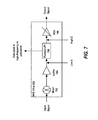
- FIG. 7 is a block diagram of a radio frequency integrated circuit (RFIC) chip with a passive low pass filter having a mismatched input and output impedance to peak or increase the gain of the passband signal at the cutoff frequency of the filter, according to an embodiment of the present invention.
- RFIC radio frequency integrated circuit
- FIG. 8 is a block diagram of a printed circuit board embodiment in which an inductor stage in the form of a passive low pass filter has been introduced on the printed circuit board between a driving chip and a loading chip to peak or increase the gain of the passband signal at the cutoff frequency of the filter, according to an embodiment of the present invention.
- the techniques may be employed in the receive chain of a millimeter wave band wireless receiver, in the transmit chain of a millimeter wave band wireless transmitter, or in both the receive chain and the transmit chain of a millimeter wave band wireless transceiver.
- the techniques include mismatching the input and output impedance of a passive low pass filter used in the chain to peak the gain of the passband signal at the cutoff frequency (Fc) of the filter.
- the millimeter wave band is the 60 GHz band and the cutoff frequency (Fc) is at or near 1 GHz.
- the techniques include driving the passive low pass filter with a low input impedance to a higher output impedance to peak or increase the gain of the passband signal at the cutoff frequency (Fc) of the filter.
- the passive low pass filter can be placed on-chip or between chips on a printed circuit board.
- the input (source) impedance is in the range of 10 to 1,000 Ohms and the output (load) impedance is the range of 100 to 10,000 Ohms and the source impedance is lower than the output impedance so as to peak or increase the gain of the passband signal at the cutoff frequency (Fc) of the filter.
- FIG. 1 it illustrates a typical 5-pole Chebyshev passive low pass filter 100 that may be used within a transmit chain or a receive chain of a millimeter wave band wireless communications device.
- Filter 100 can be used on-chip such as within a radio frequency integrated circuit (RFIC) or a baseband chip of the device.
- Filter 100 comprises four spiral inductors L 1 , L 2 , L 3 , and L 4 .
- the quality (Q) factor and self-resonant frequency (SRF) of the spiral inductors L 1 , L 2 , L 3 , and L 4 can negatively affect the flatness of the frequency response of the passband signal of the filter 100 .
- Q quality
- SRF self-resonant frequency
- the drop in the frequency response of the passband signal due to the filter 100 itself can be as much as 3 to 5 dB at the cutoff frequency (Fc) of the filter 100 .
- Additional slope in the frequency response of the passband signal can be caused by other circuits in the transmit chain or the receive chain such as mixers and baseband amplifiers.
- the input impedance and the output impedance of the filter 100 is mismatched from low to high to peak the gain of the passband signal at or near the cutoff frequency (Fc) of the filter 100 .
- FIG. 2 illustrates a 5-pole Chebyshev passive low pass filter 200 that may be used with in a transmit chain or a receive chain of a millimeter wave band wireless communications device for passband signal gain peaking, according to an embodiment of the present invention.
- a 7-pole Butterworth passive low pass filter can be used instead.
- Filter 200 can be used on-chip such as within a radio frequency integrated circuit (RFIC) or a baseband chip of the device.
- Filter 200 comprises four spiral inductors L 1 , L 2 , L 3 , and L 4 .
- the input impedance R S and the output impedance R L of filter 200 are mismatched to peak the gain in the frequency response of the passband signal at or near a cutoff frequency (Fc) of the filter 200 .
- the cutoff frequency (Fc) is at or near 1 GHz as shown in FIG. 3 .
- Mismatching the filter 200 to peak the gain involves selecting a low input impedance such that it is feasible to implement the spiral inductors L 1 , L 2 , L 3 , and L 4 on-chip.
- the input impedance to the filter 200 is selected to be in the range of 10 to 1,000 Ohms such that the filter 200 can be implemented with approximately ten (10) nano-henry (nH) spiral inductors L 1 , L 2 , L 3 , and L 4 .
- Mismatching the input and output impedance of the filter 200 to peak the gain of the passband signal also includes selecting a higher output impedance for the filter 200 that results in gain peaking of the passband signal at or near the cutoff frequency of the filter 200 .
- the selected output (load) impedance is up to an order of magnitude higher that the input (source) impedance.
- FIG. 3 is a graph 300 of the frequency response and the reflection coefficient of the filter 200 when the input impedance R S is selected at 50 Ohms and the output impedance R L is selected at 500 Ohms.
- the gain of the passband signal peaks or is increasing at the cutoff frequency (Fc) of approximately 1 GHz.
- Plot 306 charts the return loss of the filter 200 .
- FIG. 7 it is a block diagram of radio frequency integrated circuit (RFIC) chip 700 in which techniques for gain peaking may be implemented.
- the RFIC chip 700 may be included on a printed circuit board of a high-frequency wireless communications device such as, for example, a wireless communications device used for transmitting and/or receiving data wirelessly over a millimeter wave frequency band in the range of 30 to 300 GHz.
- the RFIC chip 700 comprises a mixer circuit 702 that receives an input signal and sends an output signal to a buffer circuit 704 which in turn sends an output signal to a passive low pass filter circuit 706 which in turn sends a passband signal to a variable gain amplifier circuit 708 which in turn sends an output signal from the RFIC chip 700 .
- the buffer circuit 704 or other low output impedance circuit is configured to drive the passive low pass filter circuit 706 with a relatively low input impedance in the range of 10 to 1,000 Ohms.
- the passive low pass filter circuit 706 is configured to drive the variable gain amplifier circuit 608 or other high input impedance circuit with a higher input impedance in the range of 100 to 10,000 Ohms. It has been found that this mismatch in the input and output impedance of the passive low pass filter circuit 706 causes an increase or peak in the gain of the passband signal output by the passive low pass filter circuit 706 at high-frequency cutoffs. In some embodiments, the high-frequency cutoff is at or above 1 GHz.
- PCB Printed Circuit Board
- gain peaking techniques are employed to peak the gain of a high-speed passband signal across a printed circuit board interconnection between a driving chip and a loading chip.
- the techniques can be employed to peak the gain of a high-speed passband signal across a printed circuit board interconnection between a driving radio frequency integrated circuit (RFIC) chip and a loading baseband chip.
- RFIC radio frequency integrated circuit
- the high-speed passband signal is in the range of a few hundred MHz to a few GHz.
- FIG. 4 it illustrates a typical circuit 400 in the receive or the transmit chain of a wireless communications device.
- the circuit 400 is being driven by a high-speed buffer (not shown) with a 100 Ohm output impedance.
- the buffer is driving a 4000 Ohm load through a 5 centimeter (cm) long 100 Ohm transmission line on a printed circuit board connecting a driving chip 402 and a loading chip 404 .
- the driving chip 402 may be a radio frequency integrated circuit (RFIC) chip, for example.
- the loading chip 404 may be a baseband chip, for example.
- the frequency response of the signal through the printed circuit board interconnection is plotted as line 608 in graph 600 .
- the ripple due to the transmission line on the printed circuit board and the packaging parasitics of the driving chip and the loading chip are suppressed by introducing an inductor stage in the form of a passive low pass filter on the printed circuit board between the driving chip and the loading chip.
- the input and output impedance of the passive low pass filter is mismatched to peak the gain of the passband signal of the filter at or near the cutoff frequency (Fc) of the filter.
- FIG. 5 illustrates a circuit 500 in the receive or the transmit chain of a wireless communications device, according to an embodiment of the present invention.
- the circuit 500 is being driven by a high-speed buffer (not shown) with a 100 Ohm output impedance driving a 4000 Ohm load through a 5 centimeter (cm) long 100 Ohm transmission line on a printed circuit board.
- An inductor stage in the form of a passive low pass filter 506 is added on the printed circuit board between the driving chip 502 and the loading chip 504 .
- a mismatched input (source) and output (load) impedance for the filter 506 is used. More specifically, the source impedance of the filter 506 is selected to be lower by an order of magnitude or less than the load impedance of the filter 506 . The result is a peak in the gain of the frequency response of the passband signal of the filter 506 that is fed to the loading chip 504 as shown in line 606 of chart 600 in FIG. 6 .
- the input source impedance of the filter 506 is in the range of 10 to 1,000 Ohms and the output load impedance of the filter 506 is in the range of 100 to 10,000 Ohms.
- FIG. 8 it illustrates a printed circuit board (PCB) 820 embodiment in which an inductor stage in the form of a passive low pass filter 822 is inserted on the PCB 820 in between a driving chip 810 and a loading chip 830 to peak or increase the gain of the passband signal at the cutoff frequency.
- PCB printed circuit board
- the driving chip 810 is radio frequency integrated circuit (RFIC) chip comprising a mixer 811 connected to a buffer 812 which is connected to a filter 813 which is connected to a variable gain amplifier 814 .
- the filter 813 is a passive low pass filter configured to peak or increase the gain of the passband signal sent to the VGA 814 as described above with respect to FIG. 7 .
- gain peaking techniques can be employed 1) on-chip 810 to peak or increase the gain at the cutoff frequency of the passband signal sent from filter 813 to VGA 814 and 2) on the printed circuit board 820 to peak or increase the gain at the cutoff frequency of the passband signal sent from passive low pass filter 822 to the loading chip 830 .
- the loading chip 830 is a baseband chip comprising an amplifier 831 and an analog-to-digital converter 832 .
- filter 813 could be an active low pass filter according to the requirements of the particular implementation at hand.
- a load of 4000 Ohms is driven through the transmission line 821 having a length of 5 centimeters and a resistance of 100 Ohms.
- the input source impedance and the output load impedance of the low passive filter 822 are mismatched to peak or increase the gain of the passband signal of the filter 822 at the cutoff frequency.
- the input source impedance is in the range of 10 to 1,000 Ohms and the output source impedance is in the range of 100 to 10,000 Ohms and the input source impedance is lower than the output source impedance.
- the cutoff frequency is at or above 1 GHz.
- Embodiments of the invention are particularly suited for low-power 60 GHz or millimeter wave radio applications.
- one suitable use for some embodiments of the present invention may be in battery-operated mobile wireless communications devices, such as enabling cell phones or laptop computers to wirelessly transmit large amounts of data, such as transmitting compressed or uncompressed video files to a video projector or monitor.
Landscapes
- Engineering & Computer Science (AREA)
- Computer Networks & Wireless Communication (AREA)
- Signal Processing (AREA)
- Transmitters (AREA)
- Transceivers (AREA)
Abstract
Description
Claims (7)
Priority Applications (1)
| Application Number | Priority Date | Filing Date | Title |
|---|---|---|---|
| US14/471,213 US9859862B2 (en) | 2014-08-28 | 2014-08-28 | Gain peaking techniques in high-frequency passive low pass filters |
Applications Claiming Priority (1)
| Application Number | Priority Date | Filing Date | Title |
|---|---|---|---|
| US14/471,213 US9859862B2 (en) | 2014-08-28 | 2014-08-28 | Gain peaking techniques in high-frequency passive low pass filters |
Publications (2)
| Publication Number | Publication Date |
|---|---|
| US20160065163A1 US20160065163A1 (en) | 2016-03-03 |
| US9859862B2 true US9859862B2 (en) | 2018-01-02 |
Family
ID=55403731
Family Applications (1)
| Application Number | Title | Priority Date | Filing Date |
|---|---|---|---|
| US14/471,213 Expired - Fee Related US9859862B2 (en) | 2014-08-28 | 2014-08-28 | Gain peaking techniques in high-frequency passive low pass filters |
Country Status (1)
| Country | Link |
|---|---|
| US (1) | US9859862B2 (en) |
Cited By (1)
| Publication number | Priority date | Publication date | Assignee | Title |
|---|---|---|---|---|
| US11817247B2 (en) | 2022-01-21 | 2023-11-14 | G & W Electric Company | Automatic calibration system and method for passive low-power voltage transformer |
Citations (6)
| Publication number | Priority date | Publication date | Assignee | Title |
|---|---|---|---|---|
| US3886469A (en) * | 1973-01-17 | 1975-05-27 | Post Office | Filter networks |
| US3974461A (en) * | 1974-06-14 | 1976-08-10 | Moog Music, Inc. | Wide dynamic range voltage controlled filter for electronic musical instruments |
| US5099204A (en) * | 1990-10-15 | 1992-03-24 | Qualcomm Incorporated | Linear gain control amplifier |
| US5889436A (en) * | 1996-11-01 | 1999-03-30 | National Semiconductor Corporation | Phase locked loop fractional pulse swallowing frequency synthesizer |
| US20080117000A1 (en) * | 2006-11-22 | 2008-05-22 | Fujitsu Media Devices Limited | Filter device |
| US20090189715A1 (en) * | 2008-01-29 | 2009-07-30 | Tdk Corporation | Layered low-pass filter |
-
2014
- 2014-08-28 US US14/471,213 patent/US9859862B2/en not_active Expired - Fee Related
Patent Citations (6)
| Publication number | Priority date | Publication date | Assignee | Title |
|---|---|---|---|---|
| US3886469A (en) * | 1973-01-17 | 1975-05-27 | Post Office | Filter networks |
| US3974461A (en) * | 1974-06-14 | 1976-08-10 | Moog Music, Inc. | Wide dynamic range voltage controlled filter for electronic musical instruments |
| US5099204A (en) * | 1990-10-15 | 1992-03-24 | Qualcomm Incorporated | Linear gain control amplifier |
| US5889436A (en) * | 1996-11-01 | 1999-03-30 | National Semiconductor Corporation | Phase locked loop fractional pulse swallowing frequency synthesizer |
| US20080117000A1 (en) * | 2006-11-22 | 2008-05-22 | Fujitsu Media Devices Limited | Filter device |
| US20090189715A1 (en) * | 2008-01-29 | 2009-07-30 | Tdk Corporation | Layered low-pass filter |
Cited By (1)
| Publication number | Priority date | Publication date | Assignee | Title |
|---|---|---|---|---|
| US11817247B2 (en) | 2022-01-21 | 2023-11-14 | G & W Electric Company | Automatic calibration system and method for passive low-power voltage transformer |
Also Published As
| Publication number | Publication date |
|---|---|
| US20160065163A1 (en) | 2016-03-03 |
Similar Documents
| Publication | Publication Date | Title |
|---|---|---|
| KR102362459B1 (en) | Adaptive load for coupler in broadband multimode multi-band front end module | |
| US20120050122A1 (en) | Antenna module and impedance matching method thereof | |
| US20170077966A1 (en) | Adaptive load for coupler in broadband multimode multiband front end module | |
| CN114172472B (en) | Wireless amplifier circuit for carrier aggregation | |
| US10074903B2 (en) | Antenna apparatus | |
| CN105049068A (en) | Bypass path loss reduction | |
| TW201717543A (en) | Circuits and methods for reducing insertion loss effects associated with radio-frequency power couplers | |
| US11799511B2 (en) | Transceiver having radio-frequency front-end circuit, dedicated radio-frequency front-end circuit, and switchable matching circuit integrated in same chip | |
| CN105306626A (en) | Mobile wireless communications device with improved broadband antenna impedance matching | |
| KR101444551B1 (en) | Power amplifying circuit and front end module including the same | |
| US10348251B2 (en) | Power supply circuit | |
| US9819077B1 (en) | Multi-feed antenna optimized for non-50 Ohm operation | |
| US9859862B2 (en) | Gain peaking techniques in high-frequency passive low pass filters | |
| US9825606B2 (en) | Wireless communication device and filter thereof | |
| CN104320154A (en) | Multi-mode multi-frequency front-end device | |
| US10701693B2 (en) | Bias T circuit | |
| KR101552896B1 (en) | Ultra wideband amplifier | |
| TWI462537B (en) | Communication apparatus and radio frequency equalizer | |
| KR102732400B1 (en) | Radio-frequency power amplifier with amplitude modulation to phase modulation (ampm) compensation | |
| US9893750B2 (en) | Tunable transmit cancellation in acoustic receiver filters | |
| US10171112B2 (en) | RF multiplexer with integrated directional couplers | |
| TWI544754B (en) | A wireless transceiver device with frequency band matching adjustment function and its adjustment method | |
| US11043927B2 (en) | Signal amplification structure and communication device | |
| US8669829B2 (en) | Multi-octave power amplifier | |
| CN115811280A (en) | Radio frequency power amplifier with amplitude modulation to phase modulation (AMPM) compensation |
Legal Events
| Date | Code | Title | Description |
|---|---|---|---|
| AS | Assignment |
Owner name: NITERO PTY LTD., AUSTRALIA Free format text: ASSIGNMENT OF ASSIGNORS INTEREST;ASSIGNORS:CAMILLERI, NATALINO;ZHANG, FAN;SIGNING DATES FROM 20140823 TO 20140828;REEL/FRAME:033631/0486 |
|
| AS | Assignment |
Owner name: ADVANCED MICRO DEVICES, INC., CALIFORNIA Free format text: ASSIGNMENT OF ASSIGNORS INTEREST;ASSIGNORS:NITERO, INC.;NITERO PTY. LTD.;REEL/FRAME:041966/0913 Effective date: 20170302 Owner name: AMD FAR EAST LTD., AUSTRALIA Free format text: ASSIGNMENT OF ASSIGNORS INTEREST;ASSIGNORS:NITERO, INC.;NITERO PTY. LTD.;REEL/FRAME:041966/0913 Effective date: 20170302 |
|
| STCF | Information on status: patent grant |
Free format text: PATENTED CASE |
|
| MAFP | Maintenance fee payment |
Free format text: PAYMENT OF MAINTENANCE FEE, 4TH YEAR, LARGE ENTITY (ORIGINAL EVENT CODE: M1551); ENTITY STATUS OF PATENT OWNER: LARGE ENTITY Year of fee payment: 4 |
|
| FEPP | Fee payment procedure |
Free format text: MAINTENANCE FEE REMINDER MAILED (ORIGINAL EVENT CODE: REM.); ENTITY STATUS OF PATENT OWNER: LARGE ENTITY |
|
| LAPS | Lapse for failure to pay maintenance fees |
Free format text: PATENT EXPIRED FOR FAILURE TO PAY MAINTENANCE FEES (ORIGINAL EVENT CODE: EXP.); ENTITY STATUS OF PATENT OWNER: LARGE ENTITY |
|
| STCH | Information on status: patent discontinuation |
Free format text: PATENT EXPIRED DUE TO NONPAYMENT OF MAINTENANCE FEES UNDER 37 CFR 1.362 |
|
| FP | Lapsed due to failure to pay maintenance fee |
Effective date: 20260102 |