US9857624B2 - Liquid crystal display panel and fabrication method thereof - Google Patents
Liquid crystal display panel and fabrication method thereof Download PDFInfo
- Publication number
- US9857624B2 US9857624B2 US14/985,271 US201514985271A US9857624B2 US 9857624 B2 US9857624 B2 US 9857624B2 US 201514985271 A US201514985271 A US 201514985271A US 9857624 B2 US9857624 B2 US 9857624B2
- Authority
- US
- United States
- Prior art keywords
- polarizer
- angle
- liquid crystal
- display panel
- crystal display
- Prior art date
- Legal status (The legal status is an assumption and is not a legal conclusion. Google has not performed a legal analysis and makes no representation as to the accuracy of the status listed.)
- Expired - Fee Related, expires
Links
Images


Classifications
-
- G—PHYSICS
- G02—OPTICS
- G02F—OPTICAL DEVICES OR ARRANGEMENTS FOR THE CONTROL OF LIGHT BY MODIFICATION OF THE OPTICAL PROPERTIES OF THE MEDIA OF THE ELEMENTS INVOLVED THEREIN; NON-LINEAR OPTICS; FREQUENCY-CHANGING OF LIGHT; OPTICAL LOGIC ELEMENTS; OPTICAL ANALOGUE/DIGITAL CONVERTERS
- G02F1/00—Devices or arrangements for the control of the intensity, colour, phase, polarisation or direction of light arriving from an independent light source, e.g. switching, gating or modulating; Non-linear optics
- G02F1/01—Devices or arrangements for the control of the intensity, colour, phase, polarisation or direction of light arriving from an independent light source, e.g. switching, gating or modulating; Non-linear optics for the control of the intensity, phase, polarisation or colour
- G02F1/13—Devices or arrangements for the control of the intensity, colour, phase, polarisation or direction of light arriving from an independent light source, e.g. switching, gating or modulating; Non-linear optics for the control of the intensity, phase, polarisation or colour based on liquid crystals, e.g. single liquid crystal display cells
- G02F1/133—Constructional arrangements; Operation of liquid crystal cells; Circuit arrangements
- G02F1/1333—Constructional arrangements; Manufacturing methods
- G02F1/1335—Structural association of cells with optical devices, e.g. polarisers or reflectors
- G02F1/133528—Polarisers
-
- G—PHYSICS
- G02—OPTICS
- G02F—OPTICAL DEVICES OR ARRANGEMENTS FOR THE CONTROL OF LIGHT BY MODIFICATION OF THE OPTICAL PROPERTIES OF THE MEDIA OF THE ELEMENTS INVOLVED THEREIN; NON-LINEAR OPTICS; FREQUENCY-CHANGING OF LIGHT; OPTICAL LOGIC ELEMENTS; OPTICAL ANALOGUE/DIGITAL CONVERTERS
- G02F1/00—Devices or arrangements for the control of the intensity, colour, phase, polarisation or direction of light arriving from an independent light source, e.g. switching, gating or modulating; Non-linear optics
- G02F1/01—Devices or arrangements for the control of the intensity, colour, phase, polarisation or direction of light arriving from an independent light source, e.g. switching, gating or modulating; Non-linear optics for the control of the intensity, phase, polarisation or colour
- G02F1/13—Devices or arrangements for the control of the intensity, colour, phase, polarisation or direction of light arriving from an independent light source, e.g. switching, gating or modulating; Non-linear optics for the control of the intensity, phase, polarisation or colour based on liquid crystals, e.g. single liquid crystal display cells
- G02F1/133—Constructional arrangements; Operation of liquid crystal cells; Circuit arrangements
- G02F1/1333—Constructional arrangements; Manufacturing methods
- G02F1/1335—Structural association of cells with optical devices, e.g. polarisers or reflectors
- G02F1/133509—Filters, e.g. light shielding masks
- G02F1/133514—Colour filters
- G02F1/133516—Methods for their manufacture, e.g. printing, electro-deposition or photolithography
-
- G—PHYSICS
- G02—OPTICS
- G02F—OPTICAL DEVICES OR ARRANGEMENTS FOR THE CONTROL OF LIGHT BY MODIFICATION OF THE OPTICAL PROPERTIES OF THE MEDIA OF THE ELEMENTS INVOLVED THEREIN; NON-LINEAR OPTICS; FREQUENCY-CHANGING OF LIGHT; OPTICAL LOGIC ELEMENTS; OPTICAL ANALOGUE/DIGITAL CONVERTERS
- G02F1/00—Devices or arrangements for the control of the intensity, colour, phase, polarisation or direction of light arriving from an independent light source, e.g. switching, gating or modulating; Non-linear optics
- G02F1/01—Devices or arrangements for the control of the intensity, colour, phase, polarisation or direction of light arriving from an independent light source, e.g. switching, gating or modulating; Non-linear optics for the control of the intensity, phase, polarisation or colour
- G02F1/13—Devices or arrangements for the control of the intensity, colour, phase, polarisation or direction of light arriving from an independent light source, e.g. switching, gating or modulating; Non-linear optics for the control of the intensity, phase, polarisation or colour based on liquid crystals, e.g. single liquid crystal display cells
- G02F1/133—Constructional arrangements; Operation of liquid crystal cells; Circuit arrangements
- G02F1/1333—Constructional arrangements; Manufacturing methods
- G02F1/1337—Surface-induced orientation of the liquid crystal molecules, e.g. by alignment layers
- G02F1/133753—Surface-induced orientation of the liquid crystal molecules, e.g. by alignment layers with different alignment orientations or pretilt angles on a same surface, e.g. for grey scale or improved viewing angle
-
- G—PHYSICS
- G02—OPTICS
- G02F—OPTICAL DEVICES OR ARRANGEMENTS FOR THE CONTROL OF LIGHT BY MODIFICATION OF THE OPTICAL PROPERTIES OF THE MEDIA OF THE ELEMENTS INVOLVED THEREIN; NON-LINEAR OPTICS; FREQUENCY-CHANGING OF LIGHT; OPTICAL LOGIC ELEMENTS; OPTICAL ANALOGUE/DIGITAL CONVERTERS
- G02F1/00—Devices or arrangements for the control of the intensity, colour, phase, polarisation or direction of light arriving from an independent light source, e.g. switching, gating or modulating; Non-linear optics
- G02F1/01—Devices or arrangements for the control of the intensity, colour, phase, polarisation or direction of light arriving from an independent light source, e.g. switching, gating or modulating; Non-linear optics for the control of the intensity, phase, polarisation or colour
- G02F1/13—Devices or arrangements for the control of the intensity, colour, phase, polarisation or direction of light arriving from an independent light source, e.g. switching, gating or modulating; Non-linear optics for the control of the intensity, phase, polarisation or colour based on liquid crystals, e.g. single liquid crystal display cells
- G02F1/133—Constructional arrangements; Operation of liquid crystal cells; Circuit arrangements
- G02F1/1333—Constructional arrangements; Manufacturing methods
- G02F1/1335—Structural association of cells with optical devices, e.g. polarisers or reflectors
- G02F1/133528—Polarisers
- G02F1/133538—Polarisers with spatial distribution of the polarisation direction
-
- G—PHYSICS
- G02—OPTICS
- G02F—OPTICAL DEVICES OR ARRANGEMENTS FOR THE CONTROL OF LIGHT BY MODIFICATION OF THE OPTICAL PROPERTIES OF THE MEDIA OF THE ELEMENTS INVOLVED THEREIN; NON-LINEAR OPTICS; FREQUENCY-CHANGING OF LIGHT; OPTICAL LOGIC ELEMENTS; OPTICAL ANALOGUE/DIGITAL CONVERTERS
- G02F1/00—Devices or arrangements for the control of the intensity, colour, phase, polarisation or direction of light arriving from an independent light source, e.g. switching, gating or modulating; Non-linear optics
- G02F1/01—Devices or arrangements for the control of the intensity, colour, phase, polarisation or direction of light arriving from an independent light source, e.g. switching, gating or modulating; Non-linear optics for the control of the intensity, phase, polarisation or colour
- G02F1/13—Devices or arrangements for the control of the intensity, colour, phase, polarisation or direction of light arriving from an independent light source, e.g. switching, gating or modulating; Non-linear optics for the control of the intensity, phase, polarisation or colour based on liquid crystals, e.g. single liquid crystal display cells
- G02F1/133—Constructional arrangements; Operation of liquid crystal cells; Circuit arrangements
- G02F1/1333—Constructional arrangements; Manufacturing methods
- G02F1/1337—Surface-induced orientation of the liquid crystal molecules, e.g. by alignment layers
- G02F1/133753—Surface-induced orientation of the liquid crystal molecules, e.g. by alignment layers with different alignment orientations or pretilt angles on a same surface, e.g. for grey scale or improved viewing angle
- G02F1/133757—Surface-induced orientation of the liquid crystal molecules, e.g. by alignment layers with different alignment orientations or pretilt angles on a same surface, e.g. for grey scale or improved viewing angle with different alignment orientations
-
- G02F2001/133538—
-
- G02F2001/133757—
Definitions
- the present disclosure generally relates to the field of display technologies and, more particularly, relates to a liquid crystal display panel and a fabrication method thereof.
- a liquid crystal display device mainly includes a liquid crystal display panel and a back light module.
- the back light module is the light source that provides the light to illuminate the liquid crystal display panel.
- the light emitted out of the liquid crystal display panel is modulated by the liquid crystal display panel to display images.
- FIG. 1 illustrates a schematic view of a liquid crystal display panel.
- a liquid crystal display panel includes a liquid crystal cell 100 and two polarizers 101 and 102 attached to the upper and lower sides of the liquid crystal cell 100 .
- the liquid crystal cell 100 includes a color filter.
- the light emitted from the back light module passes through the color filter and is mixed together to display various colors.
- the displayed colors reproduce the natural colors as much as possible.
- the displayed colors are adjusted to approximate the desired colors to satisfy user's requirements and to adapt to the specific application environment of the liquid crystal display panel.
- FIG. 2 illustrates a schematic view of a CIE-xy chromaticity diagram.
- the diagram represents a given color in chromaticity hue and saturation position in the color base coordinate system.
- the R, G, and B points in the diagram represent the three primary colors, red, green, and blue respectively in a certain color display system. All the colors on the sides of the triangle RGB or inside the triangle RGB may be represented in a proper mixture of the three primary colors.
- the white color with the maximum brightness is represented at the point W where all three primary colors reach the maximum brightness.
- the white color W point is in the vicinity of the triangle RGB centroid.
- an optimized and requirement satisfying white color point is obtained by adjusting the maximum brightness of the R, G, and B points.
- the thicknesses of the red color barriers, green color barriers, and blue color barriers in the color filter are adjusted to optimize the white color point. For example, increasing the thickness of the green color barriers may decrease the light-transmittance of the green color barriers and thereby reduce the maximum brightness of the green light.
- the method of matching the white color point by adjusting the thicknesses of the color barriers may have certain limitations. For example, after the thicknesses of the color barriers are determined, the brightness of the color barriers cannot be changed. When the color display system has additional special requirement for the white color point, further adjustment of the thicknesses of the color barriers to optimize the white color point may cause substantial differences in the thicknesses of the color barriers and thereby may affect the display effect.
- color barrier thickness adjustment method Another drawback of the color barrier thickness adjustment method is that each white color point designed for a certain specification requires a matching color filter with fixed thicknesses of the color barriers. As a result, liquid crystal display panels with different product specifications may need different color filters. The inability of sharing a common color filter across different liquid crystal display panel products may increase the production cost.
- the disclosed liquid crystal display panel and fabrication method are directed to solve one or more problems in the art.
- the present disclosure provides a liquid crystal display panel and a fabrication method to improve image viewing experience.
- the liquid crystal display panel includes an upper substrate configured with a color filter having a plurality of first color barriers, second color barriers, and third color barriers, a lower substrate configured with a thin film transistor array facing toward the upper substrate, a liquid crystal layer sandwiched between the upper substrate and the lower substrate, an upper polarizer disposed on the upper substrate having a second absorption axis, a lower polarizer disposed on the lower substrate having a first absorption axis that is orthogonal to the second absorption axis, and a regionalized polarizer having a plurality of first polarizing units, second polarizing units, and third polarizing units with polarization directions forming a first angle, a second angle, and a third angle with the polarization direction of the upper polarizer respectively.
- the fabrication method includes forming an upper substrate with a color filter having a plurality of first color barriers, second color barriers, and third color barriers; and forming a lower substrate with a thin film transistor array facing toward the upper substrate; forming an upper polarizer on the upper substrate having a second absorption axis.
- the fabrication method also includes forming a lower polarizer on the lower substrate having a first absorption axis that is orthogonal to the second absorption axis; and forming a regionalized polarizer between the upper polarizer and the lower polarizer on the upper substrate or the lower substrate.
- the regionalized polarizer has a plurality of first polarizing units, second polarizing units, and third polarizing units with polarization directions forming a first angle, a second angle, and a third angle with the polarization direction of the upper polarizer, respectively.
- the fabrication method includes dropping liquid crystals on the upper substrate or the lower substrate, and bonding the upper substrate and the lower substrate together to form the liquid crystal display panel.
- FIG. 1 illustrates a schematic view of a liquid crystal display panel
- FIG. 2 illustrates a schematic view of a CIE-xy chromaticity diagram
- FIG. 3 illustrates a schematic view of an exemplary liquid crystal display panel according to the disclosed embodiments
- FIG. 4 illustrates a schematic view of an exemplary regionalized polarizer according to the disclosed embodiments
- FIG. 5 illustrates a schematic view of more specific polarization relationship between a regionalized polarizer, a color filter, and an upper polarizer according to the present disclosed embodiments
- FIG. 6 illustrates a schematic view of another exemplary liquid crystal display panel according to the disclosed embodiments.
- FIG. 7 a illustrates a schematic view of an exemplary method of fabricating first polarizing units according to the disclosed embodiments
- FIG. 7 b illustrates a schematic view of an exemplary method of fabricating second polarizing units according to the disclosed embodiments
- FIG. 7 c illustrates a schematic view of an exemplary method of fabricating third polarizing units according to the disclosed embodiments
- FIG. 8 illustrates an exemplary fabrication process of a liquid crystal display panel according to the disclosed embodiments
- FIG. 9 illustrates an exemplary fabrication process of a regionalized polarizer of the liquid crystal display panel according to the disclosed embodiments.
- FIG. 10 illustrates another exemplary fabrication process of a regionalized polarizer of the liquid crystal display panel.
- FIG. 3 illustrates a schematic view of an exemplary liquid crystal display panel according to the present disclosure.
- the liquid crystal display panel may include a lower polarizer 40 , a lower substrate 21 , an upper substrate 22 , an upper polarizer 50 , and a liquid crystal layer 20 sandwiched between the lower substrate 21 and the upper substrate 22 .
- Other components may also be included.
- the lower substrate 21 may be configured with an actively driven thin film transistor array to form an array substrate.
- the lower polarizer 40 may be attached to the side of the lower substrate 21 opposite to the thin film transistor array side and facing away from the liquid crystal layer 20 .
- the upper substrate 22 may be configured with a color filter 30 for displaying colors to form a color film substrate.
- the upper polarizer 50 may be attached to the side of the upper substrate 22 opposite to the color filter side and facing away from the liquid crystal layer 20 .
- the lower substrate 21 may include a transparent base substrate 210 .
- the transparent base substrate 210 may be sequentially configured with an active layer (not shown), a gate insulating layer 212 , and a first insulating layer 213 .
- Data lines 25 may be formed on the first insulating layer 213 .
- a lower planarization layer 214 may be formed on the data lines 25 and the first insulating layer 213 .
- the lower planarization layer 214 may also provide a polarizing function. That is, a regionalized polarizer 10 may be formed coplanar with the lower planarization layer 214 .
- a plurality of first electrodes 215 and second electrodes 217 may be formed on the planarization layer 214 .
- the first electrodes 215 and the second electrodes 217 may be separated and insulated by a second insulating layer 216 .
- the second insulating layer 216 may be formed on the first electrodes 215 and the lower planarization layer 214 .
- a lower alignment layer 218 may be formed on the second electrodes 217 and the second insulating layer 216 .
- the lower alignment layer 218 may contact the liquid crystal layer 20 .
- the lower alignment layer 218 may be configured to provide an initial alignment direction to the liquid crystal molecules on the side of liquid crystal layer 20 facing toward the lower substrate 21 .
- the lower planarization layer 214 may be made mainly of a mixture of acrylic resin, naphthoquinone diazide ester, 1,4-dioxane, coupling agent, diethylene glycol ethyl methyl ether, and propylene glycol methyl ether acetate, etc.
- the fluidity of the mixture may be desirable for filling and smoothing the gaps and steps caused by the thickness differences when the data lines 25 and the gate insulating layer 212 , etc. are formed.
- the lower planarization layer 214 may have a flat top surface.
- the first electrodes 215 When the first electrodes 215 are formed on the lower planarization layer 214 , the first electrodes 215 may also have flat top surfaces. Subsequently, a uniform distance between the first electrodes 215 and the second electrodes 217 may be obtained to increase the distribution uniformity of the electric field between the first electrodes 215 and the second electrodes 217 .
- the lower planarization layer 214 may be used to reduce the coupling capacitances between the first electrodes 215 and metal lines such as the data lines 25 to improve the display effect of the liquid crystal display panel. Further, the lower planarization layer 214 may be made of an organic film forming material doped with a dichroic organic dye. When the organic film coating process is completed, a regionalized polarizer 10 with a plurality of regions with different polarization directions may be formed through an optical alignment process.
- the first electrodes 215 may be common electrodes, and the second electrodes 217 may be pixel electrodes.
- the first electrodes 215 and the second electrodes 217 may be used to provide the liquid crystal display panel with a horizontal electric field parallel to the surface of the lower substrate 21 to drive the liquid crystal molecules in the liquid crystal layer 20 to rotate to alter the polarization direction of the incidental light passing through the liquid crystal layer 20 .
- the upper substrate 22 may include a transparent base substrate 220 .
- a color filter 30 , an upper planarization layer 221 , and an upper alignment layer 222 may be formed sequentially on the transparent base substrate 220 .
- the upper alignment layer 222 may contact the liquid crystal layer 20 to provide an initial alignment direction to the liquid crystal molecules on the side of the liquid crystal layer 20 facing toward the upper substrate 22 .
- the upper alignment layer 222 may have a rubbing direction parallel with the rubbing direction of the lower alignment layer 218 .
- the color filter 30 may include a plurality of color barriers, corresponding to a plurality of sub-pixel units enclosed by metal lines such as gate lines 25 on the lower substrate 21 .
- the color filter 30 may include a plurality of first color barriers 31 , second color barriers 32 , and third color barriers 33 for displaying various colors.
- the first color barriers 31 , the second color barriers 32 , and the third color barriers 33 may be arranged alternately and repeatedly in rows on the color filter 30 .
- Color barriers displaying a same color may be arranged in columns on the color filter 30 .
- first color barriers 31 may be arranged in one column
- second color barriers 32 may be arranged in adjacent column.
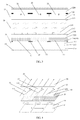
- the regionalized polarizer 10 has the polarization direction configuration illustrated in FIG. 4 and FIG. 5 .
- FIG. 4 illustrates a schematic view of an exemplary regionalized polarizer according to the present disclosure.
- the liquid crystal display panel may include an upper polarizer 50 , a regionalized polarizer 10 , and a lower polarizer 40 .
- the upper polarizer 50 may have a second absorption axis 51 in the same direction for the entire surface.
- the lower polarizer 40 may have a first absorption axis 41 in the same direction for the entire surface.
- the second absorption axis 51 and the first absorption axis 41 may be orthogonal with each other. That is, the upper polarizer 50 and the lower polarizer 40 may have mutually orthogonal polarization directions.
- the regionalized polarizer 10 may include a plurality of first polarizing units 11 , second polarizing units 12 , and third polarizing units 13 .
- the first polarizing unit 11 may have an absorption axis 111 , which may form an angle with the second absorption axis 51 .
- the second polarizing unit 12 may have an absorption axis or sub-axis 121 , which may form an angle with the second absorption axis or sub-axis 51 .
- the third polarizing unit 13 may have an absorption axis or sub-axis 131 , which may also form an angle with the second absorption axis 51 .
- FIG. 5 illustrates a schematic view of more specific polarization relationship between a regionalized polarizer, a color filter, and an upper polarizer according to the present disclosure.
- the first polarizing unit 11 may correspond to the first color barrier 31
- the second polarizing unit 12 may correspond to the second color barriers 32
- the third polarizing unit 13 may correspond to the third color barriers 33 .
- the first polarizing units 11 , the second polarizing units 12 , and the third polarizing units 13 may have a first absorption sub-axis 111 , a second absorption sub-axis 121 , and a third absorption sub-axis respectively.
- first absorption sub-axis 111 , the second absorption sub-axis 121 , and the third absorption sub-axis may form a first angle ⁇ 1 , a second angle ⁇ 2 , and a third angle ⁇ 3 respectively with the first absorption axis 51 . That is, the first polarizing units 11 , the second polarizing units 12 , and the third polarizing units 13 may have the polarization directions forming the first angle ⁇ 1 , the second angle ⁇ 2 , and the third angle ⁇ 3 respectively with the polarization direction of the upper polarizer 50 .
- the first absorption sub-axis 111 , the second absorption sub-axis 121 , and the third absorption sub-axis 131 are parallel with the first absorption axis 51 . That is, the entire surface of the regionalized polarizer 10 has the same polarization direction as the polarization direction of the upper polarizer 50 .
- the liquid crystal molecules in the liquid crystal layer 20 are driven by the electric field between the first electrodes 215 and the second electrodes 217 .
- the liquid crystal molecules on the surfaces of the upper substrate 22 and the lower substrate 21 may be arranged in the alignment directions of the upper alignment layer 222 on the upper substrate 22 and the lower alignment layer 218 on the lower substrate 21 , respectively. That is, the liquid crystal molecules on the substrate surfaces may be arranged in the polarization direction of the lower polarizer 40 .
- the liquid crystal display panel is in a dark state.
- the liquid crystal molecules in the liquid crystal layer 20 may rotate in a plane parallel with the surfaces of the upper substrate 22 and the lower substrate 21 .
- the liquid crystal molecules may be aligned in a direction forming an angle approximately between 0° and 45° with the polarization directions of the upper polarizer 50 and the lower polarizer 40 .
- An incidental light may pass through the lower polarizer 40 to produce a linearly polarized light in the polarization direction of the lower polarizer 40 .
- the linearly polarized light may continue to pass through the liquid crystal molecules and may have the polarization direction rotated by the liquid crystal molecules.
- the polarized light may continue to pass through the color filter, the regionalized polarizer 10 and the upper polarizer 50 and may exit the liquid crystal display panel to display images.
- the liquid crystal display panel may have the maximum light transmittance. That is, the liquid crystal display panel may reach the maximum brightness.
- the upper polarizer 50 and the lower polarizer in the path of the light may be required to have mutually orthogonal polarization directions.
- the angles between the polarization directions of the polarizers in the path of the incident light may be controlled to adjust the light transmittance of the liquid crystal display panel. Maximum brightness of the incident light can be adjusted by adjusting the light transmittance of the incident light.
- the first angle ⁇ 1 , the second angle ⁇ 2 , and the third angle ⁇ 3 may be controlled to adjust the light transmittances in regions of the liquid crystal display panel corresponding to the first color barriers 31 , the second color barriers 32 , and the third color barriers 33 , and hence to adjust the maximum brightness of the colors corresponding to the first color barriers 31 , the second color barriers 32 , and the third color barriers 33 to obtain the desired white color point.
- the present disclosure does not have any limitation on the relationship among the first angle ⁇ 1 , the second angle ⁇ 2 , and the third angle ⁇ 3 .
- the product specification may determine that the first angle ⁇ 1 is equal to the third angle ⁇ 3 , and the second angle ⁇ 2 is different from the first angle ⁇ 1 and the third angle ⁇ 3 .
- the product specification may determine the first angle ⁇ 1 , the second angle ⁇ 2 , and the third angle ⁇ 3 are different from each other as long as the desired white color point is obtained for the liquid crystal display panel.
- the first color barriers 31 , the second color barriers 32 , and the third color barriers 33 are corresponding to red color barriers (R), green color barriers (G), and blue color barriers (B).
- the first polarizing units, the second polarizing units, and the third polarizing units are arranged corresponding to the first color barriers 31 , the second color barriers 32 , and the third color barriers 33 , respectively.
- the white color point of the liquid crystal display panel may need to be yellowish, i.e., the maximum brightness of the red light and the blue light may be increased.
- the third angle ⁇ 3 may remain the same while the first angle ⁇ 1 and the second angle ⁇ 2 may be reduced by a same or different amount. Accordingly, the light transmittances in the regions of the liquid crystal display panel corresponding to the red color barriers (R) and the green color barriers (G) may be increased by a same or different amount, and hence the maximum brightness of the red color light and the green color light may be increased to obtain the desired white color point.
- the white color point of the liquid crystal display panel may need to be purplish.
- the second angle ⁇ 2 may remain the same while the first angle ⁇ 1 and the third angle ⁇ 3 may be reduced by a same or different amount.
- the light transmittances in the regions of the liquid crystal display panel corresponding to the red color barriers (R) and the blue color barriers (B) may be increased by a same or different amount, and hence the maximum brightness of the red color light and the blue color light may be increased to obtain the desired white color point.
- the upper polarizer is used to configure the first angle ⁇ 1 , the second angle ⁇ 2 , and the third angle ⁇ 3
- the lower polarizer may also be used to configure the first angle ⁇ 1 , the second angle ⁇ 2 , and the third angle ⁇ 3 .
- the initial values of the first angle ⁇ 1 , the second angle ⁇ 2 , and the third angle ⁇ 3 may be pre-configured.
- an optical alignment process may be used to form the polarizing units of the regionalized polarizer.
- An organic film forming material may be coated over the substrate.
- a polarized ultra violet light may be irradiated on the organic material film to form one polarizing unit at a time.
- Each polarizing unit may have different polarization direction.
- the organic material film may be cured to form the regionalized polarizer. Once cured, the polarization direction in each polarizing unit may be fixed. Once the polarization direction in each polarizing unit is fixed, the light transmittance in the region corresponding to the polarizing unit may be fixed. Accordingly, the maximum brightness of each color corresponding to each color barrier may be fixed. Thus, the white color point may be fixed as well.
- the white color point may be adjusted without sophisticated thickness control of the color barriers of the color filter.
- the white color point may be adjusted by controlling the polarization direction of the polarized ultra violet light during the optical alignment process for fabricating the regionalized polarizer.
- the upper polarizer 50 and the lower polarizer 40 may have mutually orthogonal polarization directions to ensure that the liquid crystal display panel supports the dark state.
- the regionalized polarizer 10 may have different polarization directions in different regions forming different angles with the polarization direction of the upper polarizer 50 .
- the light transmittances in the regions corresponding to different colors may be adjusted to obtain the desired white color point by controlling the first angle ⁇ 1 , the second angle ⁇ 2 , and the third angle ⁇ 3 . Since the white color point is not adjusted by controlling the thicknesses of color barriers, the desired white color point may be obtained while the flatness of the color filter is maintained to improve the display effect.
- different color filters are not needed to obtain different white color points based on different product specifications. Thus, the same color filter may be used commonly for various display products and the production cost may be reduced.
- FIG. 6 illustrates a schematic view of another exemplary liquid crystal display panel according to the present disclosure. Referring to FIG. 6 , the liquid crystal display panel is similar to the liquid crystal display panel shown in FIG. 3 with the exception of the position of the regionalized polarizer 10 .
- the regionalized polarizer 10 may be coplanar with the upper planarization layer 221 on the upper substrate 22 . Because the regionalized polarizer 10 is formed coplanar with either the upper planarization layer 221 or the lower planarization layer 214 , no additional layer may be introduced in the fabrication process. Thus, the overall thickness of the liquid crystal display panel may not increase.
- the regionalized polarizer 10 is not limited to be coplanar with the lower planarization layer 214 on the lower substrate 21 or the upper planarization layer 221 . In other embodiments, the regionalized polarizer 10 may be formed separately on the lower substrate 21 or on the upper substrate 22 rather than coplanar with any existing layer in the liquid crystal display panel.
- the present disclosure also provides a method for fabricating the disclosed liquid crystal display panel.
- the method is illustrated in fabricating the liquid crystal display panel shown in FIG. 3 .
- FIG. 8 illustrates an exemplary fabrication process of a liquid crystal display panel according to the present disclosure.
- the fabrication method may include the following steps.
- Step S 801 forming an upper substrate configured with a color filter having a plurality of first color barriers, second color barriers, and third color barriers.
- the upper substrate 22 may include a transparent base substrate 220 .
- a color filter 30 , an upper planarization layer 221 , and an upper alignment layer 222 may be formed sequentially on the transparent base substrate 220 .
- Step S 802 forming a lower substrate configured with a thin film transistor array facing toward the upper substrate.
- the lower substrate 21 may include a transparent base substrate 210 .
- the transparent base substrate 210 may be sequentially configured with an active layer, a gate insulating layer 212 , and a first insulating layer 213 .
- Data lines 25 may be formed on the first insulating layer 213 .
- Step S 803 forming an upper polarizer on the upper substrate having a second absorption axis.
- an upper polarizer 50 may be formed on the side of the upper substrate 22 facing away from the liquid crystal layer 20 .
- Step S 804 forming a lower polarizer on the lower substrate having a first absorption axis that is orthogonal to the second absorption axis.
- a lower planarization layer 214 may be formed on the data lines 25 and the first insulating layer 213 .
- a lower polarizer 40 may be formed on the side of the lower substrate 21 facing away from the liquid crystal layer 20 .
- the lower polarizer 40 may have a polarization direction orthogonal to the polarization direction of the upper polarizer 50 .
- Step S 805 forming a regionalized polarizer between the upper polarizer and the lower polarizer on the upper substrate or the lower substrate having a plurality of first polarizing units, second polarizing units, and third polarizing units with polarization directions forming a first angle, a second angle, and a third angle with the polarization direction of the upper polarizer, respectively.
- the lower planarization layer 214 may also provide a polarizing function. That is, a regionalized polarizer 10 may be formed coplanar with the lower planarization layer 214 . Alternatively, the regionalized polarizer 10 may be formed as an independent layer anywhere between the upper polarizer 50 and the lower polarizer 40 .
- Step S 806 dropping liquid crystals on the upper substrate or the lower substrate, and bonding the upper substrate and the lower substrate together to form the liquid crystal display panel.
- liquid crystals may be dropped onto one of the upper or the lower substrate, and the upper and the lower substrates may be bonded together to form the liquid crystal display panel.
- Other processes may also be performed to form other components of the liquid crystal display panel.
- FIG. 9 illustrates an exemplary fabrication process of a regionalized polarizer of the liquid crystal display panel according to the present disclosure.
- the process of fabricating the lower substrate may include forming the coplanar lower planarization layer 214 and the regionalized polarizer 10 .
- the process for fabricating the coplanar lower planarization layer 214 and the regionalized polarizer 10 may include the following steps.
- FIG. 7 a , FIG. 7 b , and FIG. 7 c illustrate schematic views of various fabrication stages and/or configurations.
- Step S 901 spin coating an organic film forming material on the entire substrate already formed with data lines.
- an acrylic resin solution including a mixture of acrylic resin, naphthoquinone diazide ester, 1,4-dioxane, coupling agent, diethylene glycol ethyl methyl ether, and propylene glycol methyl ether acetate may be provided.
- an optical alignment prepolymer doped with a dichroic organic dye may be mixed in certain proportions with the acrylic resin solution described above to produce an organic film forming material.
- the organic film forming material may be spin coated over the entire surface of the substrate.
- the dichroic organic dye may be directly mixed with the acrylic resin solution described above to produce the organic film forming material.
- the optical alignment prepolymer may be a photosensitive polyimide
- the dichroic organic dye may be an azo dye.
- Step S 902 pre-baking the organic film forming material coated over the entire surface of the substrate to form a lower planarization layer.
- the acrylic resin solution described above may fill and smooth the gaps and steps caused by the thickness differences when the gate insulating layer 212 and the first insulating layer 213 are formed through a CVD process.
- a flat surface lower planarization layer 214 may be obtained.
- Step S 903 providing an ultra violet light source emitting an ultra violet light with a wavelength range, for example, approximately between 254 nm and 313 nm, to pass through a polarizer G, for example, a metal grating polarizer to produce a first linearly polarized light R 1 . Then, the first linearly polarized light R 1 may pass through a first mask M 1 and may irradiate the lower planarization layer 214 .
- a polarizer G for example, a metal grating polarizer to produce a first linearly polarized light R 1 .
- the first linearly polarized light R 1 may pass through a first mask M 1 and may irradiate the lower planarization layer 214 .
- the first mask M 1 may have a light-transmitting portion T 1 and the rest of the first mask M 1 may be a light-shielding portion.
- the first linearly polarized light R 1 may pass through the light-transmitting portion T 1 of the first mask M 1 to irradiate the portion of the lower planarization layer 214 that overlaps with the light-transmitting portion T 1 .
- the dichroic organic dye in the portion of the lower planarization layer 214 exposed to the first linearly polarized light R 1 may be aligned to a certain polarization direction.
- the first polarizing units 11 may be formed, as show in FIG. 7 a.
- the first polarizing units 11 may have a polarization direction forming a first angle ⁇ 1 with the polarization direction of the upper polarizer 50 . Further, referring to FIG. 7 a, the plurality of first polarizing units 11 may be formed coplanar with the lower planarization layer 214 .
- Step S 904 adjusting the relative position between the polarizer G and the substrate formed with the first polarizing units 11 on the lower planarization player 214 by horizontally rotating the substrate by an angle, or horizontally rotating the polarizer G by an angle without changing the substrate position, and replacing the first mask M 1 with a second mask M 2 between the polarizer G and the lower planarization layer 214 .
- the second mask M 2 may have a light-transmitting portion T 2 and the rest of the second mask M 2 may be a light-shielding portion.
- a second linearly polarized light R 2 may be produced after the ultra violet light passes through the polarizer G.
- the second linearly polarized light R 2 may pass through the light-transmitting portion T 2 of the second mask M 2 to irradiate the portion of the lower planarization layer 214 that overlaps with the light-transmitting portion T 2 .
- the dichroic organic dye in the portion of the lower planarization layer 214 exposed to the second linearly polarized light R 2 may be aligned to a different polarization direction.
- second polarizing units 12 may be formed, as shown in FIG. 7 b.
- the second polarizing units 12 may have a polarization direction forming a second angle ⁇ 2 with the polarization direction of the upper polarizer 50 . Further, referring to FIG. 7 b, the plurality of second polarizing units 12 may be formed coplanar with the lower planarization layer 214 already formed with the first polarizing units 11 .
- Step S 905 further adjusting the relative position between the polarizer G and the substrate formed with the first polarizing units 11 and the second polarizing units 12 on the lower planarization player 214 by horizontally rotating the substrate by another angle, or horizontally rotating the polarizer G by another angle without changing the substrate position, and replacing the second mask M 2 with a third mask M 3 between the polarizer G and the lower planarization layer 214 .
- the third mask M 3 may have a light-transmitting portion T 3 and the rest of the second mask M 3 may be a light-shielding portion.
- a third linearly polarized light R 3 may be produced after the ultra violet light passes through the polarizer G.
- the third linearly polarized light R 3 may pass through the light-transmitting portion T 3 of the third mask M 3 to irradiate the portion of the lower planarization layer 214 that overlaps with the light-transmitting portion T 3 .
- the dichroic organic dye in the portion of the lower planarization layer 214 exposed to the third linearly polarized light R 3 may be aligned to another different polarization direction.
- third polarizing units 13 may be formed, as shown in FIG. 7 c.
- the third polarizing units 13 may have a polarization direction forming a third angle ⁇ 3 with the polarization direction of the upper polarizer 50 . Further, referring to FIG. 7 c, the plurality of third polarizing units 13 may be formed coplanar with the lower planarization layer 214 already formed with the first polarizing units 11 and the second polarizing units 12 .
- Step S 906 curing the lower planarization layer 214 formed with the polarizing units by performing a second high temperature baking.
- the second baking may have a high temperature approximately at 230° C.
- the curing may enhance the anisotropy feature of the first polarizing units 11 , the second polarizing units 12 , and the third polarizing units 13 .
- a regionalized polarizer 10 may be formed coplanar with the lower planarization layer 214 .
- the present disclosure provides another method for fabricating the liquid crystal display panel.
- the regionalized polarizer 10 may be formed as an independent layer rather than being coplanar with any existing layer in the upper or lower substrate.
- the fabrication method according to the present disclosure may include a process of fabricating the lower substrate, a process of fabricating the upper substrate, and a process of dropping liquid crystals and bonding the lower substrate and the upper substrate together.
- FIG. 10 illustrates another exemplary fabrication process of a regionalized polarizer of the liquid crystal display panel according to the present disclosure.
- the process for fabricating the regionalized polarizer 10 on one of the upper or lower substrate may include the following steps.
- Step S 1001 spin coating an organic film forming material doped with a dichroic organic dye on the entire surface of the substrate.
- the organic film forming material may be a photosensitive polyimide, and the dichroic organic dye may be an azo dye.
- Step S 1002 providing an ultra violet light source emitting an ultra violet light with a wavelength range, for example, approximately between 254 nm and 313 nm, to pass through a polarizer G, for example, a metal grating polarizer to produce a first linearly polarized light R 1 . Then, the first linearly polarized light R 1 may pass through a first mask M 1 and may irradiate the organic material film.
- a polarizer G for example, a metal grating polarizer to produce a first linearly polarized light R 1 .
- the first linearly polarized light R 1 may pass through a first mask M 1 and may irradiate the organic material film.
- the first mask M 1 may have a light-transmitting portion T 1 and the rest of the first mask M 1 may be a light-shielding portion.
- the first linearly polarized light R 1 may pass through the light-transmitting portion T 1 of the first mask M 1 to irradiate the portion of the organic material film that overlaps with the light-transmitting portion T 1 .
- the dichroic organic dye in the portion of the organic material film exposed to the first linearly polarized light R 1 may be aligned to a certain polarization direction.
- the first polarizing units 11 may be formed.
- the first polarizing units 11 may have a polarization direction forming a first angle ⁇ 1 with the polarization direction of the upper polarizer 50 . Referring to FIG. 7 a, the plurality of first polarizing units 11 may be formed on the substrate.
- Step S 1003 adjusting the relative position between the polarizer G and the substrate formed with the first polarizing units 11 by horizontally rotating the substrate by an angle, or horizontally rotating the polarizer G by an angle without changing the substrate position, and replacing the first mask M 1 with a second mask M 2 between the polarizer G and the organic material film.
- the second mask M 2 may have a light-transmitting portion T 2 and the rest of the second mask M 2 may be a light-shielding portion.
- a second linearly polarized light R 2 may be produced after the ultra violet light passes through the polarizer G.
- the second linearly polarized light R 2 may pass through the light-transmitting portion T 2 of the second mask M 2 to irradiate the portion of the organic material film that overlaps with the light-transmitting portion T 2 .
- the dichroic organic dye in the portion of the organic material film exposed to the second linearly polarized light R 2 may be aligned to a different polarization direction.
- second polarizing units 12 may be formed.
- the second polarizing units 12 may have a polarization direction forming a second angle ⁇ 2 with the polarization direction of the upper polarizer 50 .
- the plurality of second polarizing units 12 may be formed on the substrate already formed with the first polarizing units 11 .
- Step S 1004 further adjusting the relative position between the polarizer G and the substrate formed with the first polarizing units 11 and the second polarizing units 12 by horizontally rotating the substrate by another angle, or horizontally rotating the polarizer G by another angle without changing the substrate position, and replacing the second mask M 2 with a third mask M 3 between the polarizer G and the organic material film.
- the third mask M 3 may have a light-transmitting portion T 3 and the rest of the second mask M 3 may be a light-shielding portion.
- a third linearly polarized light R 3 may be produced after the ultra violet light passes through the polarizer G.
- the third linearly polarized light R 3 may pass through the light-transmitting portion T 3 of the third mask M 3 to irradiate the portion of the organic material film that overlaps with the light-transmitting portion T 3 .
- the dichroic organic dye in the portion of the organic material film exposed to the third linearly polarized light R 3 may be aligned to another different polarization direction.
- third polarizing units 13 may be formed.
- the third polarizing units 13 may have a polarization direction forming a third angle ⁇ 3 with the polarization direction of the upper polarizer 50 .
- the plurality of third polarizing units 13 may be formed on the substrate already formed with the first polarizing units 11 and the second polarizing units 12 .
- Step S 1005 curing the organic material film formed with the polarizing units by performing a high temperature baking.
- the baking may have a high temperature approximately at 230°.
- the curing may enhance the anisotropy feature of the first polarizing units 11 , the second polarizing units 12 , and the third polarizing units 13 .
- a regionalized polarizer 10 may be formed.
- the first angle ⁇ 1 , the second angle ⁇ 2 , and the third angle ⁇ 3 may be determined by the product specification.
- the liquid crystal display panels may be fabricated with the white color point satisfying the corresponding product specification.
- the liquid crystal display panel according to the present disclosure may include an upper polarizer, a lower polarizer, and a regionalized polarizer.
- the regionalized polarizer may include a plurality of first polarizing units, second polarizing units, and third polarizing units corresponding to a plurality of first color barriers, second color barriers, and third color barriers respectively.
- the first polarizing units, the second polarizing units, and the third polarizing units may have polarization directions forming a first angle, a second angle, and a third angle with the polarization direction of the upper polarizer respectively.
- the first angle, the second angle, and the third angle may be controlled to adjust the light transmittances in the regions of the liquid crystal display panel corresponding to the first color barriers, the second color barriers, and the third color barriers, and hence to adjust the maximum brightness of the colors corresponding to the first color barriers, the second color barriers, and the third color barriers.
- the desired white color point may be obtained in the liquid crystal display panel to satisfy the display product specification.
- the white color point is not adjusted by controlling the thicknesses of color barriers, the desired white color point may be obtained while the flatness of the color filter is maintained to improve the display effect.
- different color filters are not needed to obtain different white color points based on different product specifications.
- the same color filter may be used commonly for various display products and the production cost may be reduced.
Landscapes
- Physics & Mathematics (AREA)
- Nonlinear Science (AREA)
- Optics & Photonics (AREA)
- Crystallography & Structural Chemistry (AREA)
- Chemical & Material Sciences (AREA)
- General Physics & Mathematics (AREA)
- Mathematical Physics (AREA)
- Engineering & Computer Science (AREA)
- Spectroscopy & Molecular Physics (AREA)
- Manufacturing & Machinery (AREA)
- Liquid Crystal (AREA)
- Polarising Elements (AREA)
- Devices For Indicating Variable Information By Combining Individual Elements (AREA)
- Microelectronics & Electronic Packaging (AREA)
Abstract
Description
Claims (18)
Applications Claiming Priority (3)
| Application Number | Priority Date | Filing Date | Title |
|---|---|---|---|
| CN2015-10078157.0 | 2015-02-13 | ||
| CN201510078157.0A CN104765184B (en) | 2015-02-13 | 2015-02-13 | Liquid crystal display panel |
| CN201510078157 | 2015-02-13 |
Publications (2)
| Publication Number | Publication Date |
|---|---|
| US20160238884A1 US20160238884A1 (en) | 2016-08-18 |
| US9857624B2 true US9857624B2 (en) | 2018-01-02 |
Family
ID=53647115
Family Applications (1)
| Application Number | Title | Priority Date | Filing Date |
|---|---|---|---|
| US14/985,271 Expired - Fee Related US9857624B2 (en) | 2015-02-13 | 2015-12-30 | Liquid crystal display panel and fabrication method thereof |
Country Status (2)
| Country | Link |
|---|---|
| US (1) | US9857624B2 (en) |
| CN (1) | CN104765184B (en) |
Cited By (2)
| Publication number | Priority date | Publication date | Assignee | Title |
|---|---|---|---|---|
| US10310348B2 (en) | 2009-10-16 | 2019-06-04 | Semiconductor Energy Laboratory Co., Ltd. | Liquid crystal display device and electronic apparatus having the same |
| US10895777B1 (en) * | 2019-09-24 | 2021-01-19 | Coretronic Corporation | Display device and method for adjusting chromaticity of display beam |
Families Citing this family (7)
| Publication number | Priority date | Publication date | Assignee | Title |
|---|---|---|---|---|
| CN104597676B (en) * | 2015-02-13 | 2018-06-26 | 厦门天马微电子有限公司 | A kind of liquid crystal display panel and its manufacturing method |
| TWI560501B (en) * | 2015-06-10 | 2016-12-01 | Sumika Technology Co Ltd | Display device |
| TWI542928B (en) * | 2015-06-10 | 2016-07-21 | 住華科技股份有限公司 | Display device |
| CN105093723A (en) * | 2015-09-08 | 2015-11-25 | 深圳市华星光电技术有限公司 | Liquid crystal display panel capable of improving color error |
| CN106338862B (en) * | 2016-11-21 | 2019-06-18 | 厦门天马微电子有限公司 | A kind of display device |
| TWI630527B (en) * | 2017-09-21 | 2018-07-21 | 友達光電股份有限公司 | Display panel |
| CN115729001A (en) * | 2022-11-10 | 2023-03-03 | 广州华星光电半导体显示技术有限公司 | Display panel, preparation method thereof and display device |
Citations (2)
| Publication number | Priority date | Publication date | Assignee | Title |
|---|---|---|---|---|
| US20060023143A1 (en) * | 2004-07-27 | 2006-02-02 | Sung-Jung Lee | Liquid crystal display device having thin polarizing film and thin phase retardation film |
| US8866997B2 (en) * | 2010-11-02 | 2014-10-21 | Arizona Board Of Regents On Behalf Of The University Of Arizona | Patterned electronic and polarization optical devices |
Family Cites Families (3)
| Publication number | Priority date | Publication date | Assignee | Title |
|---|---|---|---|---|
| CN100410758C (en) * | 2005-05-27 | 2008-08-13 | 友达光电股份有限公司 | Flat panel display, liquid crystal module and method for correcting color of flat panel display |
| CN103645590B (en) * | 2013-12-12 | 2016-10-05 | 京东方科技集团股份有限公司 | A kind of array base palte and preparation method thereof, liquid crystal indicator |
| CN103926740B (en) * | 2013-12-30 | 2016-10-05 | 厦门天马微电子有限公司 | Display panel and display device |
-
2015
- 2015-02-13 CN CN201510078157.0A patent/CN104765184B/en active Active
- 2015-12-30 US US14/985,271 patent/US9857624B2/en not_active Expired - Fee Related
Patent Citations (2)
| Publication number | Priority date | Publication date | Assignee | Title |
|---|---|---|---|---|
| US20060023143A1 (en) * | 2004-07-27 | 2006-02-02 | Sung-Jung Lee | Liquid crystal display device having thin polarizing film and thin phase retardation film |
| US8866997B2 (en) * | 2010-11-02 | 2014-10-21 | Arizona Board Of Regents On Behalf Of The University Of Arizona | Patterned electronic and polarization optical devices |
Cited By (2)
| Publication number | Priority date | Publication date | Assignee | Title |
|---|---|---|---|---|
| US10310348B2 (en) | 2009-10-16 | 2019-06-04 | Semiconductor Energy Laboratory Co., Ltd. | Liquid crystal display device and electronic apparatus having the same |
| US10895777B1 (en) * | 2019-09-24 | 2021-01-19 | Coretronic Corporation | Display device and method for adjusting chromaticity of display beam |
Also Published As
| Publication number | Publication date |
|---|---|
| CN104765184B (en) | 2018-09-04 |
| CN104765184A (en) | 2015-07-08 |
| US20160238884A1 (en) | 2016-08-18 |
Similar Documents
| Publication | Publication Date | Title |
|---|---|---|
| US9575357B2 (en) | Liquid crystal display panel and fabrication method thereof | |
| US9857624B2 (en) | Liquid crystal display panel and fabrication method thereof | |
| US10429692B2 (en) | Liquid crystal display panel and fabrication method | |
| TWI421576B (en) | Liquid crystal display device with switchable viewing angle | |
| US11126042B2 (en) | Horizontal electric field type display panel, method of manufacturing the same, and display device | |
| US10295713B2 (en) | Color filter substrate, preparing method thereof, and display device | |
| WO2017005021A1 (en) | Color filter substrate, array substrate, and display panel and display apparatus having the same | |
| US9581852B2 (en) | Color filter substrate, display panel and display device | |
| US20190146271A1 (en) | Transparent liquid crystal display | |
| JP2018180290A (en) | Display device | |
| US10203545B2 (en) | Display panels and polarizers thereof | |
| US10261357B2 (en) | Displays with color filter material in border regions | |
| US10197843B2 (en) | Array substrate, color film substrate, and display device | |
| WO2017152521A1 (en) | Display device | |
| JP2016130839A (en) | Display device | |
| US8865491B2 (en) | Method for producing electro-optical device and substrate for electro-optical device | |
| US9036098B2 (en) | Liquid crystal display device and method for manufacturing the same | |
| US9964801B2 (en) | Display substrate, manufacturing method thereof and display device | |
| US20140125929A1 (en) | Liquid crystal panel, its manufacturing method, and liquid crystal display device | |
| CN114384729B (en) | Display module and manufacturing method thereof, and display device | |
| US20190123122A1 (en) | Display panel and display apparatus using the same | |
| KR100851743B1 (en) | Controllable viewing angle patterned vertical alignment liquid crystal display | |
| WO2018113061A1 (en) | Array substrate, colour film substrate and liquid crystal panel | |
| WO2020052079A1 (en) | Pixel structure and liquid crystal display device | |
| US20170097540A1 (en) | Liquid crystal display apparatus |
Legal Events
| Date | Code | Title | Description |
|---|---|---|---|
| AS | Assignment |
Owner name: XIAMEN TIANMA MICRO-ELECTRONICS CO., LTD., CHINA Free format text: ASSIGNMENT OF ASSIGNORS INTEREST;ASSIGNORS:ZHANG, LONG;ZHOU, TING;SHEN, POPING;REEL/FRAME:037387/0843 Effective date: 20151217 Owner name: TIANMA MICRO-ELECTRONICS CO., LTD., CHINA Free format text: ASSIGNMENT OF ASSIGNORS INTEREST;ASSIGNORS:ZHANG, LONG;ZHOU, TING;SHEN, POPING;REEL/FRAME:037387/0843 Effective date: 20151217 |
|
| STCF | Information on status: patent grant |
Free format text: PATENTED CASE |
|
| MAFP | Maintenance fee payment |
Free format text: PAYMENT OF MAINTENANCE FEE, 4TH YEAR, LARGE ENTITY (ORIGINAL EVENT CODE: M1551); ENTITY STATUS OF PATENT OWNER: LARGE ENTITY Year of fee payment: 4 |
|
| FEPP | Fee payment procedure |
Free format text: MAINTENANCE FEE REMINDER MAILED (ORIGINAL EVENT CODE: REM.); ENTITY STATUS OF PATENT OWNER: LARGE ENTITY |
|
| LAPS | Lapse for failure to pay maintenance fees |
Free format text: PATENT EXPIRED FOR FAILURE TO PAY MAINTENANCE FEES (ORIGINAL EVENT CODE: EXP.); ENTITY STATUS OF PATENT OWNER: LARGE ENTITY |
|
| STCH | Information on status: patent discontinuation |
Free format text: PATENT EXPIRED DUE TO NONPAYMENT OF MAINTENANCE FEES UNDER 37 CFR 1.362 |
|
| FP | Lapsed due to failure to pay maintenance fee |
Effective date: 20260102 |