US9837280B2 - Methods for manufacturing semiconductor devices - Google Patents
Methods for manufacturing semiconductor devices Download PDFInfo
- Publication number
- US9837280B2 US9837280B2 US15/229,632 US201615229632A US9837280B2 US 9837280 B2 US9837280 B2 US 9837280B2 US 201615229632 A US201615229632 A US 201615229632A US 9837280 B2 US9837280 B2 US 9837280B2
- Authority
- US
- United States
- Prior art keywords
- semiconductor
- mesas
- support structure
- forming
- trenches
- Prior art date
- Legal status (The legal status is an assumption and is not a legal conclusion. Google has not performed a legal analysis and makes no representation as to the accuracy of the status listed.)
- Expired - Fee Related, expires
Links
Images


Classifications
-
- H01L21/30604—
-
- H—ELECTRICITY
- H10—SEMICONDUCTOR DEVICES; ELECTRIC SOLID-STATE DEVICES NOT OTHERWISE PROVIDED FOR
- H10P—GENERIC PROCESSES OR APPARATUS FOR THE MANUFACTURE OR TREATMENT OF DEVICES COVERED BY CLASS H10
- H10P50/00—Etching of wafers, substrates or parts of devices
- H10P50/60—Wet etching
- H10P50/64—Wet etching of semiconductor materials
- H10P50/642—Chemical etching
-
- H—ELECTRICITY
- H10—SEMICONDUCTOR DEVICES; ELECTRIC SOLID-STATE DEVICES NOT OTHERWISE PROVIDED FOR
- H10D—INORGANIC ELECTRIC SEMICONDUCTOR DEVICES
- H10D30/00—Field-effect transistors [FET]
- H10D30/01—Manufacture or treatment
- H10D30/021—Manufacture or treatment of FETs having insulated gates [IGFET]
-
- H01L21/02532—
-
- H01L21/02658—
-
- H01L21/306—
-
- H01L21/311—
-
- H01L29/0657—
-
- H01L29/66348—
-
- H01L29/66734—
-
- H01L29/66795—
-
- H01L29/7827—
-
- H—ELECTRICITY
- H10—SEMICONDUCTOR DEVICES; ELECTRIC SOLID-STATE DEVICES NOT OTHERWISE PROVIDED FOR
- H10D—INORGANIC ELECTRIC SEMICONDUCTOR DEVICES
- H10D12/00—Bipolar devices controlled by the field effect, e.g. insulated-gate bipolar transistors [IGBT]
- H10D12/01—Manufacture or treatment
- H10D12/031—Manufacture or treatment of IGBTs
- H10D12/032—Manufacture or treatment of IGBTs of vertical IGBTs
- H10D12/038—Manufacture or treatment of IGBTs of vertical IGBTs having a recessed gate, e.g. trench-gate IGBTs
-
- H—ELECTRICITY
- H10—SEMICONDUCTOR DEVICES; ELECTRIC SOLID-STATE DEVICES NOT OTHERWISE PROVIDED FOR
- H10D—INORGANIC ELECTRIC SEMICONDUCTOR DEVICES
- H10D30/00—Field-effect transistors [FET]
- H10D30/01—Manufacture or treatment
- H10D30/021—Manufacture or treatment of FETs having insulated gates [IGFET]
- H10D30/024—Manufacture or treatment of FETs having insulated gates [IGFET] of fin field-effect transistors [FinFET]
-
- H—ELECTRICITY
- H10—SEMICONDUCTOR DEVICES; ELECTRIC SOLID-STATE DEVICES NOT OTHERWISE PROVIDED FOR
- H10D—INORGANIC ELECTRIC SEMICONDUCTOR DEVICES
- H10D30/00—Field-effect transistors [FET]
- H10D30/01—Manufacture or treatment
- H10D30/021—Manufacture or treatment of FETs having insulated gates [IGFET]
- H10D30/028—Manufacture or treatment of FETs having insulated gates [IGFET] of double-diffused metal oxide semiconductor [DMOS] FETs
- H10D30/0291—Manufacture or treatment of FETs having insulated gates [IGFET] of double-diffused metal oxide semiconductor [DMOS] FETs of vertical DMOS [VDMOS] FETs
- H10D30/0297—Manufacture or treatment of FETs having insulated gates [IGFET] of double-diffused metal oxide semiconductor [DMOS] FETs of vertical DMOS [VDMOS] FETs using recessing of the gate electrodes, e.g. to form trench gate electrodes
-
- H—ELECTRICITY
- H10—SEMICONDUCTOR DEVICES; ELECTRIC SOLID-STATE DEVICES NOT OTHERWISE PROVIDED FOR
- H10D—INORGANIC ELECTRIC SEMICONDUCTOR DEVICES
- H10D30/00—Field-effect transistors [FET]
- H10D30/60—Insulated-gate field-effect transistors [IGFET]
- H10D30/63—Vertical IGFETs
-
- H—ELECTRICITY
- H10—SEMICONDUCTOR DEVICES; ELECTRIC SOLID-STATE DEVICES NOT OTHERWISE PROVIDED FOR
- H10D—INORGANIC ELECTRIC SEMICONDUCTOR DEVICES
- H10D62/00—Semiconductor bodies, or regions thereof, of devices having potential barriers
- H10D62/10—Shapes, relative sizes or dispositions of the regions of the semiconductor bodies; Shapes of the semiconductor bodies
- H10D62/117—Shapes of semiconductor bodies
-
- H—ELECTRICITY
- H10—SEMICONDUCTOR DEVICES; ELECTRIC SOLID-STATE DEVICES NOT OTHERWISE PROVIDED FOR
- H10P—GENERIC PROCESSES OR APPARATUS FOR THE MANUFACTURE OR TREATMENT OF DEVICES COVERED BY CLASS H10
- H10P14/00—Formation of materials, e.g. in the shape of layers or pillars
- H10P14/20—Formation of materials, e.g. in the shape of layers or pillars of semiconductor materials
- H10P14/34—Deposited materials, e.g. layers
- H10P14/3402—Deposited materials, e.g. layers characterised by the chemical composition
- H10P14/3404—Deposited materials, e.g. layers characterised by the chemical composition being Group IVA materials
- H10P14/3411—Silicon, silicon germanium or germanium
-
- H—ELECTRICITY
- H10—SEMICONDUCTOR DEVICES; ELECTRIC SOLID-STATE DEVICES NOT OTHERWISE PROVIDED FOR
- H10P—GENERIC PROCESSES OR APPARATUS FOR THE MANUFACTURE OR TREATMENT OF DEVICES COVERED BY CLASS H10
- H10P14/00—Formation of materials, e.g. in the shape of layers or pillars
- H10P14/20—Formation of materials, e.g. in the shape of layers or pillars of semiconductor materials
- H10P14/36—Formation of materials, e.g. in the shape of layers or pillars of semiconductor materials characterised by treatments done before the formation of the materials
-
- H—ELECTRICITY
- H10—SEMICONDUCTOR DEVICES; ELECTRIC SOLID-STATE DEVICES NOT OTHERWISE PROVIDED FOR
- H10P—GENERIC PROCESSES OR APPARATUS FOR THE MANUFACTURE OR TREATMENT OF DEVICES COVERED BY CLASS H10
- H10P50/00—Etching of wafers, substrates or parts of devices
-
- H—ELECTRICITY
- H10—SEMICONDUCTOR DEVICES; ELECTRIC SOLID-STATE DEVICES NOT OTHERWISE PROVIDED FOR
- H10P—GENERIC PROCESSES OR APPARATUS FOR THE MANUFACTURE OR TREATMENT OF DEVICES COVERED BY CLASS H10
- H10P50/00—Etching of wafers, substrates or parts of devices
- H10P50/20—Dry etching; Plasma etching; Reactive-ion etching
- H10P50/28—Dry etching; Plasma etching; Reactive-ion etching of insulating materials
Definitions
- Embodiments of the present invention relate to methods for manufacturing semiconductor devices, in particular to a method for manufacturing field-effect semiconductor devices having a plurality of semiconductor mesas.
- JFET Junction Field Effect Transistor
- MOSFET Metal Oxide Semiconductor Field Effect Transistor
- IGBT Insulated Gate Bipolar Transistor
- TEDFET Trench Extended Drain Field-Effect Transistor
- MGFETs Multiple Gate Field-Effect Transistors
- FinFETs which are double-gate transistors that may be built on SOI substrates (silicon-on-insulator) and are characterized by conducting channels which are wrapped by a thin silicon “fin” forming the body region of the field-effect transistor.
- Forming the deeply into the semiconductor material extending high quality accumulation dielectrics may, for example for power TEDFETs of higher blocking capability, become complex, in particular for semiconductor mesas and intervening trenches of higher aspect ratios and small pitch. Due the reduced mechanical stability of semiconductor mesas with high aspect ratio, the risk of deflecting the semiconductor mesas, for example during implantation, lithography or wet-chemical etching processes of rinsing and drying or due to a vibration, increases. Deflecting may result in adherence of neighboring semiconductor mesas, for example due to capillary forces. Furthermore, a thin mesa may even break off. These risks may be reduced by replacing water as solvent, for example by using isopropanol. However, this approach is not satisfactory for deep vertical trenches and deeply into the semiconductor material extending thin dielectrics, respectively. Using thicker mesas requires larger areas and thus increases costs.
- the method includes: providing a wafer comprising an upper surface and a plurality of semiconductor mesas extending to the upper surface, adjacent pairs of the semiconductor mesas of the plurality of semiconductor mesas being separated from each other by at least one of a trench extending from the upper surface into the wafer, and a non-semiconductor region arranged on a side-wall of the trench; forming a first support structure made of a first material and adjoining the plurality of semiconductor mesas at the upper surface so that the adjacent pairs of the semiconductor mesas are bridged by the first support structure; forming a second support structure made of a second material and adjoining the plurality of semiconductor mesas at the upper surface so that the adjacent pairs of the semiconductor mesas are bridged by the second support structure; removing the first support structure; and at least partly removing the second support structure.
- the second material is different from the first material.
- the method includes: providing a wafer having an upper surface and a semiconductor layer extending to the upper surface. Etching wide trenches from the upper surface into the semiconductor layer to form first semiconductor mesas having sidewalls; forming sacrificial oxide layers on the sidewalls of the first semiconductor mesas; performing a selective epitaxial growth process to form second semiconductor mesas in the wide trenches between adjacent sacrificial oxide layers; forming on the upper surface a first support structure of an oxidizable material so that adjacent pairs of the first and second semiconductor mesas are bridged by the first support structure; removing the sacrificial oxide layers to expose sidewalls of the first and second semiconductor mesas; forming on the upper surface a second support structure of a non-oxidizable material so that adjacent pairs of the first and second semiconductor mesas are bridged by the second support structure; thermal oxidizing at least the sidewalls of the first and second semiconductor me
- the method includes: providing a wafer having an upper surface and a plurality of semiconductor mesas which extend to the upper surface and are, next to the upper surface and in a cross-section which is substantially orthogonal to the upper surface, spaced apart from each other; forming a first support structure of a first material and adjoining the plurality of semiconductor mesas at the upper surface so that adjacent pairs of the semiconductor mesas are bridged by the first support structure and that the first support structure is substantially arranged only above the upper surface; forming a second support structure of a second material and adjoining the plurality of semiconductor mesas at the upper surface so that the adjacent pairs of the semiconductor mesas are bridged by the second support structure and that the second support structure is substantially arranged only above the upper surface; processing a side wall of at least one of the plurality of semiconductor mesas; removing the first support structure; and at least partly removing the second support structure.
- the second material is different from the first material.
- the method includes: forming in a semiconductor substrate a plurality of semiconductor mesas extending to an upper side so that adjacent semiconductor mesas are spaced apart from each other by one of a substantially empty trench and a trench substantially filled with a sacrificial layer selectively etchable with respect to the semiconductor mesas; forming a support structure mechanically connecting the semiconductor mesas; and processing the semiconductor substrate from the upper side while the semiconductor mesas are mechanically connected via the support structure.
- the method includes: providing a semiconductor substrate having an upper side and comprising, in a vertical cross-section substantially orthogonal to the upper side, a plurality of semiconductor mesas of a first monocrystalline semiconductor material which are spaced apart from each other by sacrificial layers selectively etchable with respect to the first monocrystalline semiconductor material and arranged in trenches extending from the upper side into the semiconductor substrate; forming on the semiconductor mesas a support structure mechanically connecting the semiconductor mesas; at least partly replacing the sacrificial layers while the semiconductor mesas remain mechanically connected via the support structure; and at least partly removing the support structure.
- the method includes: providing a semiconductor substrate including an upper side and a semiconductor layer of a semiconductor material and extending to the upper side; etching wide trenches from the upper side into the semiconductor layer so that first semiconductor mesas are formed which are separated from each other by the wide trenches and connected by semiconductor portions of the semiconductor material; forming dielectric layers at least at sidewalls of the first semiconductor mesas; and performing a selective epitaxial growth process to fill at least one of the wide trenches with a second semiconductor mesa.
- the method includes: providing a semiconductor substrate having an upper side and including a semiconductor layer extending to the upper side; etching trenches from the upper side into the semiconductor layer so that semiconductor mesas having sidewalls are formed which are separated from each other by the trenches, each of the trenches comprising a bottom wall; forming at the upper side a support structure mechanically connecting the semiconductor mesas; and implanting dopants from the upper side into the bottom walls and/or the sidewalls while the semiconductor mesas are mechanically connected via the support structure.
- FIGS. 1 to 9 illustrate vertical cross-sections through a semiconductor body during method steps of a method according to embodiments
- FIGS. 10A and 10B illustrate plan views on a semiconductor body as illustrated in FIG. 7 according to embodiments
- FIGS. 11 to 20 illustrate vertical cross-sections through a semiconductor body during method steps of a method according to further embodiments
- FIG. 21 illustrates a perspective view of a semiconductor body during method steps of a method according to further embodiments
- FIGS. 22A and 22B illustrate plan views on a semiconductor body during method steps of a method according to further embodiments
- FIGS. 23A and 23B illustrate plan views on a semiconductor body during method steps of a method according to further embodiments
- FIGS. 24A and 24B plan views on a semiconductor body during method steps of a method according to further embodiments
- FIGS. 25A and 25B illustrate plan views on a semiconductor body during method steps of a method according to further embodiments
- FIGS. 26A and 26B illustrate vertical cross-section through a semiconductor body and a plan view on a semiconductor body during method steps of a method according to further embodiments.
- FIGS. 27A and 27B illustrate vertical cross-sections through a semiconductor body during method steps of a method according to further embodiments.
- horizontal intends to describe an orientation substantially parallel to a first or main surface or upper side of a semiconductor substrate or body. This can be for instance the surface of a wafer or a die. In the following, the main surface is also referred to as upper surface.
- vertical as used in this specification intends to describe an orientation which is substantially arranged perpendicular to the first surface, i.e. parallel to the normal direction of the first surface of the semiconductor substrate or body.
- a second surface of a semiconductor substrate of semiconductor body is considered to be formed by the lower or backside surface while the first surface is considered to be formed by the upper, front or main surface of the semiconductor substrate.
- the terms “above” and “below” as used in this specification therefore describe a relative location of a structural feature to another structural feature with consideration of this orientation.
- first conductivity type p-doped
- second conductivity type the semiconductor devices can be formed with opposite doping relations so that the first conductivity type can be n-doped and the second conductivity type can be p-doped.
- some Figures illustrate relative doping concentrations by indicating “ ⁇ ” or “+” next to the doping type.
- n- means a doping concentration which is less than the doping concentration of an “n”-doping region while an “n + ”-doping region has a larger doping concentration than the “n”-doping region.
- indicating the relative doping concentration does not mean that doping regions of the same relative doping concentration have to have the same absolute doping concentration unless otherwise stated.
- two different n + -doping regions can have different absolute doping concentrations. The same applies, for example, to an n + -doping and a p + -doping region.
- the semiconductor device typically includes a field-effect structure and an integrated free-wheeling diode.
- the field-effect structure may be a TEDFET-structure, a MOSFET or an IGBT-structure (Insulated Gate Bipolar Transistor-structure) having a pn-junction forming a body diode between a drift region of the first conductivity type and a body region of the second conductivity type.
- the semiconductor device is typically a vertical semiconductor device having two load metallizations, for example a source metallization and a drain metallization, which are arranged opposite to each other and in low resistive contact with a respective contact region.
- the semiconductor device is a power semiconductor device having an active area with a plurality of IGBT-cells, MOSFET-cells or TEDFET-cells for carrying and/or controlling a load current between the two load metallizations.
- the power semiconductor device has typically a peripheral area with at least one edge-termination structure at least partially surrounding the active area when seen from above.
- power semiconductor device intends to describe a semiconductor device on a single chip with high voltage and/or high current switching capabilities. In other words, power semiconductor devices are intended for high current, typically in the Ampere range. Within this specification the terms “power semiconductor device” and “power semiconductor component” are used synonymously.
- field-effect intends to describe the electric-field mediated formation of a conductive “channel” of a first conductivity type and/or control of conductivity and/or shape of the channel between two regions of the first conductivity type.
- the conductive channel may be formed and/or controlled in a semiconductor region of a second conductivity type, typically a body region of the second conductivity type, which is arranged between the two regions of the first conductivity type. Due to the field-effect, a unipolar current path through the channel region is formed and/or controlled between a source region or emitter region of the first conductivity type and a drift region of the first conductivity type in a MOSFET-structure and an IGBT-structure, respectively.
- the drift region may be in contact with a higher doped drain region of the first conductivity type or a higher doped collector region of the second conductivity type, respectively.
- the drain region or the collector region is in low resistive electric contact with a drain or collector electrode.
- the source region or emitter region is in low resistive electric contact with a source or emitter electrode.
- the terms “in ohmic contact”, in resistive electric contact” and “in resistive electric connection” intend to describe that there is an ohmic current path between respective elements or portions of a semiconductor device at least when no voltages or only low probe voltages are applied to and/or across the semiconductor device.
- the terms in low ohmic contact, “in low resistive electric contact” and “in low resistive electric connection” intend to describe that there is a low resistive ohmic current path between respective elements or portions of a semiconductor device at least when no voltages are applied to and/or across the semiconductor device.
- the terms “in low ohmic contact”, “in low resistive electric contact”, “electrically coupled”, and “in low resistive electric connection” are used synonymously.
- the resistivity of a low resistive current path between respective elements or portions of a semiconductor device which is low when low voltages are applied to and/or across the semiconductor device for example a probe voltage of less than one or a few volts, becomes high above a threshold voltage, for example due to depleting a semiconductor region forming at least a part of the current path.
- MOS metal-oxide-semiconductor
- MIS metal-insulator-semiconductor
- MOSFET metal-oxide-semiconductor field-effect transistor
- IGFET insulated-gate field-effect transistor
- MISFET metal-insulator-semiconductor field-effect transistor
- gate electrode intends to describe an electrode which is situated next to, and configured to form and/or control a channel region.
- the term “gate electrode” shall embrace an electrode which is situated next to, and insulated from the body region by an insulating region forming a gate dielectric region and configured to form and/or control a channel region next to a heterojunction or through the body region as well as an electrode in low resistive electric contact with a gate region adjoining a channel region of an opposite doping type and configured to shape a depleted portion in the channel region by charging to an appropriate voltage.
- the insulating region may be made of any suitable dielectric material such as silicon oxide, for example thermal silicon oxide, silicon nitride, siliconoxynitride or the like.
- the term “metallization” intends to describe a region or a layer with metallic or near metallic properties with respect to electric conductivity.
- a metallization may be in contact with a semiconductor region to form an electrode, a pad and/or a terminal of the semiconductor device.
- the metallization may be made of and/or comprise a metal such as Al, Ti, W, Cu and Co but may also be made of a material with metallic or near metallic properties with respect to electric conductivity such as highly doped n-type or p-type poly-Si, TiN or an electrically conductive silicide such as TaSi 2 , TiSi 2 , PtSi, CoSi 2 , WSi 2 or the like.
- the metallization may also include different electrically conductive materials, for example a stack of those materials.
- semiconductor mesa or “mesa region” intends to describe semiconductor regions or semiconductor portions of the semiconductor body which extend from a common substrate, for example a semiconductor substrate, to a main surface of the semiconductor body or wafer and are in respective upper portions spaced apart from each other.
- a mesa region is, in a vertical cross-section which is substantially orthogonal to the main surface, arranged between two adjacent vertical trenches extending from the main surface into the semiconductor body or wafer.
- empty trench intends to describe a trench that is at least in a vertical cross-section not filled with a solid material and shall embrace trenches filled with a gas such as air.
- a monocrystalline semiconductor region or layer is typically a monocrystalline Si-region or Si-layer. It should, however, be understood that the semiconductor body can be made of any semiconductor material suitable for manufacturing a semiconductor device.
- Such materials include, without being limited thereto, elementary semiconductor materials such as silicon (Si) or germanium (Ge), group IV compound semiconductor materials such as silicon carbide (SiC) or silicon germanium (SiGe), binary, ternary or quaternary III-V semiconductor materials such as gallium nitride (GaN), gallium arsenide (GaAs), gallium phosphide (GaP), indium phosphide (InP), indium gallium phosphide (InGaPa), aluminum gallium nitride (AlGaN), aluminum indium nitride (AlInN), indium gallium nitride (InGaN), aluminum gallium indium nitride (AlGaInN) or indium gallium arsenide phosphide (InGaAsP), and binary or ternary II-VI semiconductor materials such as cadmium telluride (CdTe) and mercury cadmium telluride (H
- heterojunction semiconductor materials include, without being limited thereto, aluminum gallium nitride (AlGaN)-aluminum gallium indium nitride (AlGaInN), indium gallium nitride (InGaN)-aluminum gallium indium nitride (AlGaInN), indium gallium nitride (InGaN)-gallium nitride (GaN), aluminum gallium nitride (AlGaN)-gallium nitride (GaN), indium gallium nitride (InGaN)-aluminum gallium nitride (AlGaN), silicon-silicon carbide (Si x C 1-x ) and silicon-SiGe heterojunction semiconductor materials.
- the semiconductor body comprises a high band gap material such as SiC or GaN which has a high breakdown voltage and high critical avalanche field strength, respectively, the doping of the respective semiconductor regions can be chosen higher which reduces the on-state resistance Ron in the following also referred to as on-resistance Ron.
- FIGS. 1 to 9 illustrate vertical cross-sections through semiconductor device 100 and a semiconductor body 40 of semiconductor device 100 , respectively.
- the semiconductor device 100 to be manufactured is typically a power semiconductor device with a plurality unit cells arranged in an active area for switching and/or controlling a vertical current.
- semiconductor device 100 is typically manufactured on wafer-level.
- the FIGS. 1 to 9 typically only represent a section through the wafer 40 .
- wafer 40 has an upper surface 101 and a plurality of semiconductor mesas 1 extending to the upper surface 101 . Adjacent pairs of the semiconductor mesas 1 are separated from each by respective trenches 50 which extend from the upper surface 101 into wafer 40 , and by non-semiconductor regions 2 arranged on the sidewalls of the trenches 50 and semiconductor mesas 1 , respectively.
- the wafer 40 may for example be a silicon wafer or a silicon-on-insulator wafer (SOI-wafer). Note that FIG. 1 only illustrates an upper portion of wafer 40 .
- the non-semiconductor regions 2 may, for example, be made of silicon oxide or carbon.
- the semiconductor mesas 1 and trenches 50 are substantially bar-shaped when seen from above.
- a first support structure 10 of a first material is typically formed at the upper surface 101 so that the adjacent pairs of the semiconductor mesas 1 are bridged by the first support structure 10 .
- forming the first support structure 10 typically includes forming a first layer 10 of the first material which adjoins each semiconductor mesas 1 and is substantially arranged only above the plurality of semiconductor mesas 1 . Accordingly, the trenches 50 remain substantially free of the first material. This facilitates further processing.
- first material is made of an oxidizable material such as carbon, or diamond-like carbon that may be formed in a CVD-process (Chemical Vapour Deposition).
- the first layer 10 may be formed as amorphous carbon using a PECVD-process (Plasma-Enhanced Chemical Vapour Deposition) in a hydrocarbon rich atmosphere.
- a mask 17 is formed on the first layer 10 as illustrated in FIG. 3 .
- This typically includes a photolithographic process.
- FIG. 4 The resulting structure is illustrated in FIG. 4 . Note that all semiconductor mesas 1 are typically bridged by the first support structure 10 . Accordingly, semiconductor mesas 1 which are not bridged by the first support structure 10 in the vertical cross-section of FIG. 4 are typically bridged in one or more different vertical cross-section. Accordingly, the semiconductor mesas 1 are mechanically stabilized.
- the vertical extension of the first support structure 10 is, depending on material properties and geometry, typically in a range from about 100 nm to about 5 ⁇ m, more typically from about 0.5 ⁇ m to about 1.5 ⁇ m to provide a sufficiently large mechanical stabilization of the mesas 1 .
- the non-semiconductor regions 2 may be etched selectively to the first support structure 10 and the semiconductor mesas 1 . This may be done by wet-chemical etching. The resulting semiconductor device 100 is illustrated in FIG. 5 .
- a second support structure 20 of a second material is typically formed on the semiconductor mesas 1 .
- forming the second support structure 20 typically includes forming a second layer 20 of the second material which adjoins the semiconductor mesas 1 at the upper surface 101 . Similar as explained above for the first layer 10 , the second layer 20 typically adjoins all semiconductor mesas 1 and is substantially arranged only above the plurality of semiconductor mesas 1 . Accordingly, the trenches 50 remain substantially free of the second material. This facilitates further processing.
- the second layer 20 is typically formed as a non-conformal layer using, for example, a CVD-process, more typically a PECVD-process.
- the second layer 20 may be formed as a non-conformal USG-Layer (Undoped-Silicate-Glass-layer) or TEOS-layer (Tetra-Ethyl-Ortho-Silicate-layer) using a CVD-process.
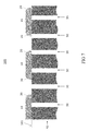
- FIG. 7 illustrates the structure after a subsequent unmasked non-isotropic selective etching process, for example by plasma etching, of the second layer 20 . Accordingly, a second support structure 20 which bridges adjacent pairs of the semiconductor mesas 1 is formed in a self-adjusted manner with respect to the first support structure 10 . Accordingly, no further photolithographic processes are required.
- the vertical extension of the second support structure 20 is, depending on material properties and geometry, typically in a range from about 100 nm to about 5 ⁇ m, more typically in a range from about 0.5 ⁇ m to about 1.5 ⁇ m to provide sufficient mechanical stability for the mesas 1 when the first support structure is subsequently removed.
- the semiconductor mesas 1 are typically substantially bar-shaped when seen from above. Furthermore, the second support structure 20 typically adjoins the first support structure 10 at this processing stage.
- the first support structure 10 and the second support structure 20 typically include, when seen from above, bar-shaped portions that are tilted with respect to the semiconductor mesas 1 , for example by a respective tilt angle in a range from about 25° to about 90°, more typically in a range from about 45° to about 90°.
- the first support structure 10 may be formed as a contiguous mesh, for example as a layer 10 with circular, ellipsoidal or polygonal holes which are partly filled with respective portions of the second support structure 20 .
- a thermal oxidizing process is performed.
- both the first support structure 10 is removed by ashing and thermal oxide layers 3 are formed on sidewalls of the semiconductor mesas 1 while the mesas 1 remain mechanically stabilized by the second support structure 20 .
- the thermal oxide layers 3 typically form high quality dielectric layers 3 of low defect density and high breakdown voltage, respectively. Forming high quality dielectric layers 3 is, however, only one example of processing the side wall the semiconductor mesas 1 and/or the side wall or bottom walls of the trenches 50 while the mesas are mechanically supported by at least one of the first support structure 10 and the second support structure 20 .
- the wafer is inherently stable and need no longer supporting structures on the upper surface 101 to mechanically stabilize the semiconductor mesas 1 .
- the semiconductor mesas 1 are stabilized without causing substantial additional wafer bow during processing the trenches 50 and semiconductor mesas 1 , respectively.
- This may be achieved by appropriate material selection and deposition conditions for forming the first and second support structures 10 , 20 .
- the second support structure 20 may be made of a non-oxidizable material such as silicon oxide, TEOS, USG (Undoped Silicate Glass), silicon nitride or the like and the first support structure 10 may be made of an oxidizable material such as carbon, for example amorphous carbon or diamond-like carbon.
- the first support structure 10 is removed and the second the second support structure 20 stabilizes the semiconductor mesas 1 without adding substantial additional mechanical stress.
- the process is neutral with respect to wafer bow.
- thermal stress during thermal oxidizing may in addition be reduced, in particular for thin wafers, by a corresponding additional layer of the material of the second support structure 20 on the back-side of the wafer.
- the materials of the first support structure 10 and the second support structures 20 may also be selectively etchable to each other.
- the first support structure 10 may be made of silicon-nitride, an imide, or silicon that is, for removing the first support structure 10 , selectively etched with respect to the second support structure 20 made of a different material such as a silicon oxide.
- the second support structure 20 may be removed.
- the resulting structure is illustrated in FIG. 9 .
- the second support structure 20 is removed by polishing, etching, and/or a CMP-process (Chemical Mechanical Polishing).
- first and second support structures 10 , 20 Due to using the first and second support structures 10 , 20 , semiconductor devices such as TEDFETs with trenches 50 and dielectric regions 3 , respectively, having high aspect ratios of more than about 10, more typically more than about 20, for example up 1000 may safely be manufactured.
- FIGS. 11 to 20 illustrating vertical cross-sections through a semiconductor body or wafer 40 , method steps of a method for forming a semiconductor device 200 are explained.
- the wafer 40 having an upper surface 101 and a semiconductor layer 1 extending to the upper surface 101 is provided.
- wide trenches 51 are etched from the upper surface 101 into the semiconductor layer 1 to form first semiconductor mesas 1 having sidewalls.
- sacrificial oxide layers (sacrificial dielectric layers) 2 may be formed on the on the sidewalls of the first semiconductor mesas 1 and wide trenches 51 , respectively.
- a selective epitaxial growth process may be performed to form second semiconductor mesas 1 in the wide trenches 51 between adjacent sacrificial oxide layers 2 .
- the resulting structure is illustrated in FIG. 11 .
- a first support structure 10 of an oxidizable material such as amorphous carbon or diamond-like carbon is formed on the upper surface 101 so that adjacent pairs of the first and second semiconductor mesas 1 are bridged by the first support structure 10 . This may be done similar as explained above with regard to FIGS. 2 to 4 .
- a first layer 10 of amorphous carbon may be deposited on the first and second mesas 1 in a CVD-process and hard-mask layer 11 of e.g. silicon oxide may be deposited on the first layer 10 .
- the resulting structure is illustrated in FIG. 12 .
- a mask 17 is formed on the hard-mask layer 11 as illustrated in FIG. 13 .
- This typically includes a photolithographic process.
- mask 17 is used to etch the hard-mask layer 11 thereby forming a hard-mask 11 .
- the resulting structure is illustrated in FIG. 14 .
- the hard-mask 11 is used to etch the first layer 10 thereby forming a first support structure 10 .
- the resulting structure is illustrated in FIG. 15 . Note that all semiconductor mesas 1 are typically bridged by the first support structure 10 . Thereafter, the hard-mask 11 may be removed
- the sacrificial oxide layers 2 may be removed by etching to expose sidewalls of the first and second semiconductor mesas 1 . In so doing vertical trenches 50 are formed between the first and second mesas 1 .
- the resulting structure 200 is illustrated in FIG. 16 .
- the first support structure 10 , 20 mechanically stabilize the first and second semiconductor mesas 1 during removing the sacrificial oxide layers 2 and typically also during further subsequent processes.
- a second support structure 20 of a second material is typically formed on the first and second semiconductor mesas 1 .
- forming the second support structure 20 typically includes forming a second layer 20 of the second material which adjoins the semiconductor mesas 1 at the upper surface 101 .
- the second layer 20 is typically formed as a non-conformal layer using, for example, a CVD-process.
- the second layer 20 may be formed as a non-conformal USG-Layer (Undoped-Silicate-Glass-layer) or TEOS-layer (Tetra-Ethyl-Ortho-Silicate-layer) using a CVD-process.
- FIG. 18 illustrates the structure after a subsequent unmasked non-isotropic selective etching process of the second layer 20 . Accordingly, a second support structure 20 which bridges adjacent pairs of the semiconductor mesas 1 is formed in a self-adjusted manner with respect to the first support structure 10 .
- first support structure 10 and the second support structure 20 typically adjoin all semiconductor mesas 1 and are substantially arranged only above the plurality of semiconductor mesas 1 . Accordingly, the trenches 50 remain substantially free of the materials of the first support structure 10 and the second support structure 20 . This facilitates further processing.
- first support structure 10 and the second support structure 20 may include adjoining bar-shaped portions that are tilt with respect to the first and second semiconductor mesas 1 similar as explained above with regard to FIG. 10A .
- the first support structure 10 may also be formed as a contiguous mesh 1 similar as explained above with regard to FIG. 10B .
- a common thermal oxidizing process may be performed to fill the vertical trenches 50 with a high quality thermal oxide layers 3 and to remove the first support structure 10 by ashing.
- the first and second semiconductor mesas 1 are mechanically stabilized by the second support structures 20 .
- the resulting structure 200 is illustrated in FIG. 19 .
- the second support structure 20 may be partly removed from the upper surface 101 .
- the resulting structure is illustrated in FIG. 20 . This may be done by polishing, etching, and/or a CMP-process. Note that the second support structure 20 and the thermal oxide 3 may also be completely removed from the upper surface 101 .
- the methods for forming the semiconductor devices 100 , 200 explained above with regard to FIGS. 1 to 10 and 11 to 20 may also be describe as providing in a first process a wafer having an upper surface 101 and a plurality of semiconductor mesas 1 extending to the upper surface 101 .
- the wafer is provided with trenches 50 extending from the upper surface 101 into the wafer and between respective pairs of semiconductor mesas 1 .
- the trenches 50 may already at least partly be filled with respective dielectric regions 2 , for example with respective carbon-layers or sacrificial silicon oxide layers covering sidewalls of the semiconductor mesas 1 and/or completely filling the vertical trenches.
- a first support structure 10 made a first material and adjoining the plurality of semiconductor mesas 1 at the upper surface 101 is typically formed such that adjacent pairs of the semiconductor mesas 1 are bridged by the first support structure 10 and that the first support structure 10 is substantially arranged only above the upper surface 101 .
- a second support structure 20 made of a second material and adjoining the plurality of semiconductor mesas 1 at the upper surface 101 is formed such that the adjacent pairs of the semiconductor mesas 1 are bridged by the second support structure 20 and that the second support structure 20 is substantially arranged only above the upper surface 101 .
- the second material is different from the first material.
- the first material may be an oxidizable material such as carbon, diamond-like carbon or silicon and the second material may be a non-oxidizable material such silicon oxide, silicon nitride or USG.
- the second material may also be selectively etchable against the first material.
- the first and second support structure 10 , 20 stabilizes the semiconductor mesas 1 during further processing, for example during further processing side walls of the semiconductor mesas 1 to form high quality dielectric regions 3 between adjacent mesas 1 . Accordingly, the breaking off mesas 1 and/or irreversible forming firm contacts between adjacent mesas 1 may be avoided. This facilitates forming of semiconductor devices such as TEDFETs with smaller pitch and/or higher aspect ratio of semiconductor mesas 1 and trenches 50 , respectively.
- the second support structure 20 is typically formed in a self-aligned manner with respect to the first support structure 10 . In so doing, only one lithographical process is required to form the first and second support structures 10 , 20 .
- support structures may be formed in a self-aligned manner with respect to the first support structure 10 and/or second support structure 20 . This increases flexibility of manufacturing without using additional photo masks.
- first support structure 10 and the second support structure 20 may be formed and at least partly removed at different manufacturing stages.
- first support structure 10 may be removed prior to or during forming the high quality dielectric regions 3 between adjacent mesas 1 , while the second support structure 20 is completely or partly removed thereafter. This increases flexibility of manufacturing and facilitates processing of high aspect ratio trenches and mesas.
- the second support structure 20 and the first support structure 10 are typically only formed substantially above the plurality of semiconductor mesas 1 . Accordingly, the mesas 1 are stabilized without filling the trenches 50 .
- Non-conformal first and second layers 10 , 20 may deposited and subsequently etched to form the first support structure 10 and the second support structure 20 , respectively.
- the second support structure 20 is formed using a CVD-process to form a non-conformal layer and an un-isotropic etching process or recess-etching of the non-conformal layer.
- the materials and/or vertical extensions and/or deposition conditions of the first support structure 10 and the second support structure 20 are chosen such that the wafer bow is not or almost not changed when the first support structure 10 and/or the second support structure 20 are arranged on the upper surface 101 .
- respective layers may also be arranged on a back-side of the wafer to further minimize the influence of the first support structure 10 and the second support structure 20 , respectively, on wafer bow.
- the first support structure 10 and the second support structure 20 may be removed from the upper surface 101 and further processes of, for example, forming field-effect structures in the mesas 1 may be performed at or close to the upper surface 101 .
- FIG. 21 shows a perspective view of a typically small portion of the semiconductor body 40 of the semiconductor device 300 and illustrates a stage after several process steps resulting in a semiconductor substrate 40 having an upper surface 101 and upper side 101 , respectively, and a plurality of semiconductor mesas 1 of a first monocrystalline semiconductor material (e.g. monocrystalline silicon) which are spaced apart from each other by sacrificial layers 2 arranged in trenches 50 and extending from the upper side 1 into the semiconductor substrate 40 , and after forming on the semiconductor mesas 1 a support structure 10 mechanically connecting each pair of adjacent semiconductor mesas 1 at the upper surface 101 .
- a first monocrystalline semiconductor material e.g. monocrystalline silicon
- the semiconductor mesas 1 extend from a common semiconductor substrate 30 to the upper surface 101 .
- the semiconductor mesas 1 may have vertical extensions h of up to several microns ( ⁇ m) and high aspect ratios h/w of more than about 10, more typically more than about 20 or 50, for example up to about 1000.
- the semiconductor device 300 to be manufactured may be a TEDFET.
- the method resulting in the structure shown in FIG. 21 may include the following steps performed after each other providing a semiconductor substrate 40 having a semiconductor layer 1 extending to the upper surface 101 ; etching wide trenches 52 from above into the semiconductor layer 1 so that first semiconductor mesas 1 (left and right ones in FIG. 21 ) are formed; forming sacrificial layers 2 (e.g.
- sacrificial dielectric layers 2 at sidewalls of the wide trenches 51 and first semiconductor mesas 1 , respectively, for example by thermal oxidation; performing a selective epitaxial growth process to form second semiconductor mesas 1 ′′ in the wide trenches 52 ; an optional CMP-process; and forming the support structure 10 bridging pairs of adjacent semiconductor mesas 1 , 1 ′′.
- the trenches 50 may be completely filled with a dielectric material and the support structure 10 at least partly be removed.
- the sidewalls and bottom walls of the trenches 50 are thermally oxidized. Accordingly, a high quality dielectric is formed that may be used as accumulation oxide of the TEDFET and possible crystal defects at or close to the sidewalls are removed.
- the trenches 50 are only partly filled.
- the partly filled trenches may include voids to reduce mechanical stress.
- filling the trenches 50 and removing the support structure 10 may be performed in a common dry-etch process or plasma process.
- the support structure 10 may be removed by etching and/or polishing, for example a CMP-process.
- the design of the support structure 10 including the material, the height and the layout when viewed from above may be chosen in accordance with expected mechanical, thermal and/or hydrodynamic loads (magnitude and/or frequency) expected during processing with recessed trench side walls and/or trench bottoms.
- FIGS. 22A and 22B show a contiguous support structure 10 and a support structure 10 of bar-shaped portions 10 bridging two or more sacrificial layers 2 (and trenches), respectively.
- the support structure 10 may also include substantially ring-shaped, circular, ellipsoidal, hexagonal or other polygonal structures.
- the semiconductor device 400 to be manufactured is typically also a TEDEFT.
- a semiconductor substrate 40 having an upper surface ( 101 ) and a semiconductor layer 1 of a semiconductor material and extending to the upper surface ( 101 ) is provided.
- wide trenches 52 may be etched from the upper surface ( 101 ) into the semiconductor layer 1 so that first semiconductor mesas 1 are formed which are separated from each other by the wide trenches 52 and connected by remaining semiconductor portions 10 of the first semiconductor layer 1 , i.e. portions 10 of the semiconductor material, typically silicon.
- the resulting semiconductor structure 400 is illustrated in FIG. 23A showing a plan view on the upper surface ( 101 ) of the semiconductor body 40 .
- spaced apart semiconductor mesas 1 and a support structure 10 therefore and extending to the upper surface are formed in a common etching process.
- the wide trenches 52 may be formed as elongated rectangles with a larger horizontal extension (width) w 1 of several ten microns up to more than about 100 ⁇ m, when viewed from above. Furthermore, the wide trenches 52 typically form at least in an active device area of unit cells a regular two-dimensional array, when viewed from above. Even further, the wide trenches 52 are typically formed such that substantially parallel first semiconductor mesas 1 are formed having a larger, for example at least three times, at least five times or even at least ten times large maximum extension than the wide trenches 52 when viewed from above.
- the semiconductor body 40 In a first vertical cross-section substantially perpendicular to the upper surface along the dashed line s 1 , the semiconductor body 40 typically has a plurality of spaced apart wide trenches 52 extending from a common substrate to the upper surface.
- the semiconductor body 40 may only include the common substrate and a contiguous remaining portion 1 , 10 of the semiconductor layer 1 extending from the common substrate to the upper surface.
- FIG. 23B The resulting semiconductor structure is illustrated in FIG. 23B .
- the first and second semiconductor mesas 1 , 15 typically form drift control zones 1 , and drift zones 15 , respectively.
- the forming of dielectric layers 3 by thermal oxidizing may result in a complete oxidizing of the semiconductor portions 10 as illustrated in FIG. 24A for the structure 401 . In so doing, edge regions of the second semiconductor mesas 15 which may have crystal defects may be removed.
- the semiconductor portions 10 and adjoining parts of the dielectric layers 3 are replaced by dielectric plugs 4 as illustrated in FIG. 24B for the structure 402 .
- This may be achieved by masked etching, depositing a dielectric material, a planarization process and/or partially back-etching the deposited dielectric material. In so doing, edge regions of the second semiconductor mesas 15 which may have crystal defects may be removed.
- FIGS. 25A and 25B method steps of a further method for forming a semiconductor device 403 are explained.
- the method is similar as explained above with regard to FIGS. 23A and 23B .
- the step of etching wide trenches 52 is performed such that the wide trenches 52 and the semiconductor portions 10 form a respective triangular lattice instead of respective rectangular lattices, when viewed from above.
- FIGS. 26A and 26B method steps of a method for forming a semiconductor device 500 are explained.
- a semiconductor substrate 40 having an upper surface 101 and a semiconductor layer 1 extending to the upper surface 101 may be provided.
- trenches 50 , 50 ′ may be etched from the upper surface 101 into the semiconductor layer 1 . Accordingly, semiconductor mesas 1 having sidewalls are formed. The semiconductor mesas 1 , 1 ′ and sidewalls, respectively, are separated from each other by the trenches 50 , 50 ′ having respective bottom walls 55 , 55 ′.
- FIGS. 26A and 26B showing a vertical cross-section (along line s) through and a plan view on the structure 500 , respectively.
- a plurality of the semiconductor mesas 1 , 1 ′ is formed typically extending from a common semiconductor layer 30 to the upper surface 101 .
- the outermost semiconductor mesas 1 ′ and the outermost trenches 50 ′ may have in the vertical cross-section of FIG. 26A have larger horizontal extensions compared to the inner semiconductor mesas 1 and inner trenches 50 , respectively.
- Forming the support structure 10 at the upper surface 101 typically includes depositing a negative resist, masked radiating the negative resist, and applying a film developer (photo developer) to form a resist structure (support structure) 10 capable of stabilizing the usually thin semiconductor mesas 1 at least during a subsequent rinsing, drying and/or a lithography performed from above.
- a film developer photo developer
- the trenches 50 , 50 ′ and semiconductor mesas 1 , 1 ′ may have a vertical extension of up to 5 ⁇ m or even more microns while the width (horizontal extension in the cross-section of FIG. 26 a ) of the semiconductor mesas 1 , 1 ′ and trenches 50 , 50 ′ may be below about 150 nm or 100 nm and below about 300 nm, respectively.
- the negative resist is radiated with a radiation having a minimum wavelength larger, for example by a factor of two or three, than the distance between adjacent semiconductor mesas 1 . Accordingly, the radiation does substantially not enter the trenches 50 , 50 ′. Accordingly, a support structure 10 may be formed which is arranged at and above the upper surface 101 , but almost not in the trenches 50 , 50 ′ as illustrated in FIGS. 26A and 26B .
- a doping step is used to implant dopants from above into the bottom walls 55 , 55 ′ and/or the mesa sidewalls while the semiconductor mesas 1 , 1 ′ are mechanically connected via the support structure 10 . If dopants are to be implanted into portions of the bottom walls 55 , 55 ′ which are shadowed by the support structure 10 in plan view, an angled implantation may be used.
- the support structure 10 may be removed, for example in a thermal process or by dry etching.
- FIGS. 27A and 27B method steps of a further method for forming a semiconductor device 501 are explained.
- the method is similar as explained above with regard to FIGS. 26A and 27B .
- the design of the support structure 10 illustrated in FIG. 27A is chosen such that the film developer cannot reach the un-cured resist in the shown right portion 50 b (right of the dashed vertical line) which may also lie behind the shown left portion 50 a . Accordingly, the trenches 50 in the portion 50 b remain filled with the resist.
- a first doping process (implantation from above) may be performed.
- the cured resist may be completely or partially removed by dry etching.
- the resulting structure 501 is illustrated in FIG. 27B .
- a second doping process (implantation from above) may be performed to implant dopants into parts of the portion 50 a shadowed during the first doping process while the portion 50 b remains shadowed.
- the uncured resist in portion 50 b may be removed.
- the risk of breaking off the mesas ( 1 ) and/or irreversibly forming firm contacts between adjacent mesas ( 1 ) during the further processing from the upper side ( 101 ) is at least substantially reduced.
- This is of particular importance for manufacturing field-effect semiconductor devices such as trench-DRAMs (Dynamic Random Access Memory), TEDETs and FinFETs having semiconductor mesas ( 1 ) of high aspect ratios, for example of at least about 10, 20 or even more, and/or small distances, for example of less than about 150 nm or even less than about 100 nm, between adjacent semiconductor mesas.
- the at least one support structure ( 10 , 20 ) may be partly or completely removed, for example after at least partly filling the trenches ( 50 ) again with a solid material such as a dielectric or poly-silicon to stabilize the semiconductor mesas ( 1 ).
- a method for forming a semiconductor device includes: forming in a semiconductor substrate ( 40 ) a plurality of semiconductor mesas ( 1 ) extending to an upper side ( 101 ) so that adjacent semiconductor mesas ( 1 ) are spaced apart from each other by a trench ( 50 ), typically an empty trench ( 50 ), a substantially empty trench ( 50 ), or a trench ( 50 ) completely or at least substantially filled with a material ( 2 ) selectively etchable with respect to the semiconductor mesas ( 1 ), for example filled with a dielectric layer ( 2 ); forming a support structure ( 10 ) mechanically connecting the semiconductor mesas ( 1 ) which are spaced apart from each other by one of the substantially empty trench ( 50 ) and the trench ( 50 ) substantially filled with the material; and processing the semiconductor substrate ( 40 ) from the upper side ( 101 ) while the semiconductor mesas ( 1 ) are mechanically connected via the support structure ( 10 ).
- a method for forming a semiconductor device includes: providing a semiconductor substrate ( 40 ) having an upper side ( 101 ) and comprising a plurality of semiconductor mesas ( 1 ) which are, in a vertical cross-section substantially orthogonal to the upper side, spaced apart from each other and extend to the upper side ( 101 ), at the upper side ( 101 ) a support structure ( 10 ) mechanically connecting the semiconductor mesas ( 1 ); and processing the semiconductor substrate ( 40 ) from the upper side ( 101 ) while the semiconductor mesas ( 1 ) remain mechanically connected via the support structure ( 10 ).
- the semiconductor mesas ( 1 ) are spaced apart from each other by trenches ( 50 ) which are at least substantially empty or at least substantially filled with a material selectively etchable with respect to a monocrystalline semiconductor material of the semiconductor mesas ( 1 ).
Landscapes
- Element Separation (AREA)
- Thin Film Transistor (AREA)
- Metal-Oxide And Bipolar Metal-Oxide Semiconductor Integrated Circuits (AREA)
- Chemical & Material Sciences (AREA)
- Chemical Kinetics & Catalysis (AREA)
- General Chemical & Material Sciences (AREA)
Abstract
Description
Claims (6)
Priority Applications (1)
| Application Number | Priority Date | Filing Date | Title |
|---|---|---|---|
| US15/229,632 US9837280B2 (en) | 2012-11-21 | 2016-08-05 | Methods for manufacturing semiconductor devices |
Applications Claiming Priority (3)
| Application Number | Priority Date | Filing Date | Title |
|---|---|---|---|
| US13/682,995 US9054123B2 (en) | 2012-11-21 | 2012-11-21 | Method for manufacturing a semiconductor device |
| US14/063,362 US9437440B2 (en) | 2012-11-21 | 2013-10-25 | Method for manufacturing a semiconductor device |
| US15/229,632 US9837280B2 (en) | 2012-11-21 | 2016-08-05 | Methods for manufacturing semiconductor devices |
Related Parent Applications (1)
| Application Number | Title | Priority Date | Filing Date |
|---|---|---|---|
| US14/063,362 Division US9437440B2 (en) | 2012-11-21 | 2013-10-25 | Method for manufacturing a semiconductor device |
Publications (2)
| Publication Number | Publication Date |
|---|---|
| US20160343577A1 US20160343577A1 (en) | 2016-11-24 |
| US9837280B2 true US9837280B2 (en) | 2017-12-05 |
Family
ID=50625743
Family Applications (2)
| Application Number | Title | Priority Date | Filing Date |
|---|---|---|---|
| US14/063,362 Active US9437440B2 (en) | 2012-11-21 | 2013-10-25 | Method for manufacturing a semiconductor device |
| US15/229,632 Expired - Fee Related US9837280B2 (en) | 2012-11-21 | 2016-08-05 | Methods for manufacturing semiconductor devices |
Family Applications Before (1)
| Application Number | Title | Priority Date | Filing Date |
|---|---|---|---|
| US14/063,362 Active US9437440B2 (en) | 2012-11-21 | 2013-10-25 | Method for manufacturing a semiconductor device |
Country Status (3)
| Country | Link |
|---|---|
| US (2) | US9437440B2 (en) |
| CN (1) | CN103839824A (en) |
| DE (1) | DE102013112862B9 (en) |
Families Citing this family (2)
| Publication number | Priority date | Publication date | Assignee | Title |
|---|---|---|---|---|
| JP6061610B2 (en) * | 2012-10-18 | 2017-01-18 | ルネサスエレクトロニクス株式会社 | Manufacturing method of semiconductor device |
| CN117954306A (en) * | 2022-10-21 | 2024-04-30 | 长鑫存储技术有限公司 | Semiconductor structure processing method and semiconductor structure |
Citations (43)
| Publication number | Priority date | Publication date | Assignee | Title |
|---|---|---|---|---|
| EP0339962A2 (en) | 1988-04-27 | 1989-11-02 | General Electric Company | Field effect semiconductor device |
| US6323090B1 (en) | 1999-06-09 | 2001-11-27 | Ixys Corporation | Semiconductor device with trenched substrate and method |
| US6528398B1 (en) | 2001-02-01 | 2003-03-04 | Advanced Micro Devices, Inc. | Thinning of trench and line or contact spacing by use of dual layer photoresist |
| US20040144985A1 (en) | 2001-06-25 | 2004-07-29 | Zhibo Zhang | Optoelectronic devices having arrays of quantum-dot compound semiconductor superlattices therein |
| US20050023571A1 (en) | 2001-09-07 | 2005-02-03 | Power Integrations, Inc. | High-voltage vertical transistor with a multi-layered extended drain structure |
| US20060189053A1 (en) * | 2005-02-22 | 2006-08-24 | Chih-Hao Wang | PMOS transistor with discontinuous CESL and method of fabrication |
| US20060209887A1 (en) | 2005-02-11 | 2006-09-21 | Alpha & Omega Semiconductor, Ltd | Shielded gate trench (SGT) MOSFET cells implemented with a schottky source contact |
| US20070026629A1 (en) * | 2005-07-29 | 2007-02-01 | Taiwan Semiconductor Manufacturing Company, Ltd. | Novel structure for a multiple-gate FET device and a method for its fabrication |
| TW200721516A (en) | 2005-11-29 | 2007-06-01 | Ind Tech Res Inst | Silicon-based photodetector and method of fabricating the same |
| CN1997588A (en) | 2004-07-09 | 2007-07-11 | 惠普开发有限公司 | Nanowire device with (111) vertical sidewalls and method of making the same |
| US20070170542A1 (en) * | 2006-01-26 | 2007-07-26 | Micron Technology, Inc. | Method of filling a high aspect ratio trench isolation region and resulting structure |
| US20070264809A1 (en) | 2006-03-07 | 2007-11-15 | International Rectifier Corporation | Process for manufacture of trench schottky |
| US20080073707A1 (en) | 2006-09-27 | 2008-03-27 | Darwish Mohamed N | Power MOSFET with recessed field plate |
| US20080076222A1 (en) | 2006-09-26 | 2008-03-27 | Infineon Technologies Austria Ag | Method for producing an integrated circuit with a trench transistor structure |
| US20080083966A1 (en) | 2006-07-28 | 2008-04-10 | Matsushita Electric Industrial Co., Ltd. | Schottky barrier semiconductor device |
| US20080087896A1 (en) | 2002-07-11 | 2008-04-17 | International Rectifier Corporation | Trench Schottky barrier diode with differential oxide thickness |
| US20080173875A1 (en) | 2006-04-14 | 2008-07-24 | Yaroslav Koshka | Self-aligned methods based on low-temperature selective epitaxial growth for fabricating silicon carbide devices |
| WO2009034658A1 (en) | 2007-09-14 | 2009-03-19 | Shindengen Electric Manufacturing Co., Ltd. | Semiconductor device |
| US20100013552A1 (en) | 2008-07-15 | 2010-01-21 | Maxpower Semiconductor Inc. | MOSFET Switch with Embedded Electrostatic Charge |
| US20100025805A1 (en) * | 2008-07-30 | 2010-02-04 | Hall Mark D | Semiconductor devices with extended active regions |
| CN101681017A (en) | 2007-05-11 | 2010-03-24 | 高通Mems科技公司 | MEMS structure, method of fabricating MEMS components on separate substrates and assembly thereof |
| US20100207205A1 (en) | 2009-02-19 | 2010-08-19 | Grebs Thomas E | Structures and Methods for Improving Trench-Shielded Semiconductor Devices and Schottky Barrier Rectifier Devices |
| US20100314707A1 (en) | 2009-06-12 | 2010-12-16 | Yedinak Joseph A | Reduced Process Sensitivity of Electrode-Semiconductor Rectifiers |
| US20100327288A1 (en) | 2009-06-26 | 2010-12-30 | Pfc Device Corporation | Trench schottky diode and method for manufacturing the same |
| US20110049532A1 (en) * | 2009-08-28 | 2011-03-03 | Microsemi Corporation | Silicon carbide dual-mesa static induction transistor |
| US20110186841A1 (en) | 2008-02-28 | 2011-08-04 | Nxp B.V. | Semiconductor device and method of manufacture thereof |
| US20110220990A1 (en) | 2010-03-11 | 2011-09-15 | Alpha And Omega Semiconductor Incorporated | Shielded gate trench mos with improved source pickup layout |
| US20110284953A1 (en) | 2010-05-21 | 2011-11-24 | SIM-BCD Semiconductor Manufacturing Limited | Power trench mosfet rectifier |
| US20120037983A1 (en) | 2010-08-10 | 2012-02-16 | Force Mos Technology Co., Ltd. | Trench mosfet with integrated schottky rectifier in same cell |
| US20120049270A1 (en) * | 2010-08-30 | 2012-03-01 | Infineon Technologies Austria Ag | Method for Forming a Semiconductor Device, and a Semiconductor with an Integrated Poly-Diode |
| US20120080748A1 (en) | 2010-09-30 | 2012-04-05 | Force Mos Technology Co., Ltd. | Trench mosfet with super pinch-off regions |
| US20120146133A1 (en) | 2010-12-10 | 2012-06-14 | Infineon Technologies Ag | Method for Producing a Semiconductor Component with Insulated Semiconductor Mesas |
| US20120181575A1 (en) * | 2011-01-17 | 2012-07-19 | Infineon Technologies Austria Ag | Semiconductor Device and a Reverse Conducting IGBT |
| US20120205772A1 (en) * | 2011-02-15 | 2012-08-16 | Tzu-Hsiung Chen | Trench schottky diode and manufacturing method thereof |
| US20120217512A1 (en) | 2009-11-19 | 2012-08-30 | Philippe Renaud | Lateral power transistor device and method of manufacturing the same |
| US20120292732A1 (en) | 2011-05-17 | 2012-11-22 | Grivna Gordon M | Semiconductor diode and method of manufacture |
| US20130105885A1 (en) * | 2011-10-27 | 2013-05-02 | Globalfoundries Inc. | Canyon gate transistor and methods for its fabrication |
| US20130181319A1 (en) | 2012-01-17 | 2013-07-18 | Richtek Technology Corporation | Trench Schottky Barrier Diode and Manufacturing Method Thereof |
| US20130221429A1 (en) | 2012-02-29 | 2013-08-29 | Robert Kuo-Chang Yang | Method and apparatus related to a junction field-effect transistor |
| US20130228891A1 (en) | 2012-03-02 | 2013-09-05 | Pfc Device Corp. | Multi-trench termination structure for semiconductor device and manufacturing mehtod thereof |
| US20130264390A1 (en) | 2010-12-16 | 2013-10-10 | 3M Innovative Properties Company | Transparent Micropatterned RFID Antenna and Articles Incorporating Same |
| US20140070309A1 (en) | 2012-09-11 | 2014-03-13 | Kabushiki Kaisha Toshiba | Semiconductor device and manufacturing method of the same |
| US20150179791A1 (en) * | 2013-04-16 | 2015-06-25 | Panasonic Intellectual Property Management Co., Ltd. | Silicon carbide semiconductor device and method for manufacturing same |
-
2013
- 2013-10-25 US US14/063,362 patent/US9437440B2/en active Active
- 2013-11-21 DE DE102013112862.9A patent/DE102013112862B9/en active Active
- 2013-11-21 CN CN201310757138.1A patent/CN103839824A/en active Pending
-
2016
- 2016-08-05 US US15/229,632 patent/US9837280B2/en not_active Expired - Fee Related
Patent Citations (44)
| Publication number | Priority date | Publication date | Assignee | Title |
|---|---|---|---|---|
| EP0339962A2 (en) | 1988-04-27 | 1989-11-02 | General Electric Company | Field effect semiconductor device |
| US6323090B1 (en) | 1999-06-09 | 2001-11-27 | Ixys Corporation | Semiconductor device with trenched substrate and method |
| US6528398B1 (en) | 2001-02-01 | 2003-03-04 | Advanced Micro Devices, Inc. | Thinning of trench and line or contact spacing by use of dual layer photoresist |
| US20040144985A1 (en) | 2001-06-25 | 2004-07-29 | Zhibo Zhang | Optoelectronic devices having arrays of quantum-dot compound semiconductor superlattices therein |
| US20050023571A1 (en) | 2001-09-07 | 2005-02-03 | Power Integrations, Inc. | High-voltage vertical transistor with a multi-layered extended drain structure |
| US20080087896A1 (en) | 2002-07-11 | 2008-04-17 | International Rectifier Corporation | Trench Schottky barrier diode with differential oxide thickness |
| CN1997588A (en) | 2004-07-09 | 2007-07-11 | 惠普开发有限公司 | Nanowire device with (111) vertical sidewalls and method of making the same |
| US20060209887A1 (en) | 2005-02-11 | 2006-09-21 | Alpha & Omega Semiconductor, Ltd | Shielded gate trench (SGT) MOSFET cells implemented with a schottky source contact |
| US20060189053A1 (en) * | 2005-02-22 | 2006-08-24 | Chih-Hao Wang | PMOS transistor with discontinuous CESL and method of fabrication |
| US20070026629A1 (en) * | 2005-07-29 | 2007-02-01 | Taiwan Semiconductor Manufacturing Company, Ltd. | Novel structure for a multiple-gate FET device and a method for its fabrication |
| TW200721516A (en) | 2005-11-29 | 2007-06-01 | Ind Tech Res Inst | Silicon-based photodetector and method of fabricating the same |
| US20070170542A1 (en) * | 2006-01-26 | 2007-07-26 | Micron Technology, Inc. | Method of filling a high aspect ratio trench isolation region and resulting structure |
| US20070264809A1 (en) | 2006-03-07 | 2007-11-15 | International Rectifier Corporation | Process for manufacture of trench schottky |
| US20080173875A1 (en) | 2006-04-14 | 2008-07-24 | Yaroslav Koshka | Self-aligned methods based on low-temperature selective epitaxial growth for fabricating silicon carbide devices |
| US20080083966A1 (en) | 2006-07-28 | 2008-04-10 | Matsushita Electric Industrial Co., Ltd. | Schottky barrier semiconductor device |
| US20080076222A1 (en) | 2006-09-26 | 2008-03-27 | Infineon Technologies Austria Ag | Method for producing an integrated circuit with a trench transistor structure |
| US20080073707A1 (en) | 2006-09-27 | 2008-03-27 | Darwish Mohamed N | Power MOSFET with recessed field plate |
| CN101852914A (en) | 2007-05-11 | 2010-10-06 | 高通Mems科技公司 | Microelectromechanical system structures, methods of fabricating microelectromechanical system components on separate substrates and assemblies thereof |
| CN101681017A (en) | 2007-05-11 | 2010-03-24 | 高通Mems科技公司 | MEMS structure, method of fabricating MEMS components on separate substrates and assembly thereof |
| WO2009034658A1 (en) | 2007-09-14 | 2009-03-19 | Shindengen Electric Manufacturing Co., Ltd. | Semiconductor device |
| US20110186841A1 (en) | 2008-02-28 | 2011-08-04 | Nxp B.V. | Semiconductor device and method of manufacture thereof |
| US20100013552A1 (en) | 2008-07-15 | 2010-01-21 | Maxpower Semiconductor Inc. | MOSFET Switch with Embedded Electrostatic Charge |
| US20100025805A1 (en) * | 2008-07-30 | 2010-02-04 | Hall Mark D | Semiconductor devices with extended active regions |
| US20100207205A1 (en) | 2009-02-19 | 2010-08-19 | Grebs Thomas E | Structures and Methods for Improving Trench-Shielded Semiconductor Devices and Schottky Barrier Rectifier Devices |
| US20100314707A1 (en) | 2009-06-12 | 2010-12-16 | Yedinak Joseph A | Reduced Process Sensitivity of Electrode-Semiconductor Rectifiers |
| US20100327288A1 (en) | 2009-06-26 | 2010-12-30 | Pfc Device Corporation | Trench schottky diode and method for manufacturing the same |
| US20110049532A1 (en) * | 2009-08-28 | 2011-03-03 | Microsemi Corporation | Silicon carbide dual-mesa static induction transistor |
| US20120217512A1 (en) | 2009-11-19 | 2012-08-30 | Philippe Renaud | Lateral power transistor device and method of manufacturing the same |
| US20110220990A1 (en) | 2010-03-11 | 2011-09-15 | Alpha And Omega Semiconductor Incorporated | Shielded gate trench mos with improved source pickup layout |
| US20110284953A1 (en) | 2010-05-21 | 2011-11-24 | SIM-BCD Semiconductor Manufacturing Limited | Power trench mosfet rectifier |
| US20120037983A1 (en) | 2010-08-10 | 2012-02-16 | Force Mos Technology Co., Ltd. | Trench mosfet with integrated schottky rectifier in same cell |
| US20120049270A1 (en) * | 2010-08-30 | 2012-03-01 | Infineon Technologies Austria Ag | Method for Forming a Semiconductor Device, and a Semiconductor with an Integrated Poly-Diode |
| US20120080748A1 (en) | 2010-09-30 | 2012-04-05 | Force Mos Technology Co., Ltd. | Trench mosfet with super pinch-off regions |
| US20120146133A1 (en) | 2010-12-10 | 2012-06-14 | Infineon Technologies Ag | Method for Producing a Semiconductor Component with Insulated Semiconductor Mesas |
| US20130264390A1 (en) | 2010-12-16 | 2013-10-10 | 3M Innovative Properties Company | Transparent Micropatterned RFID Antenna and Articles Incorporating Same |
| US20120181575A1 (en) * | 2011-01-17 | 2012-07-19 | Infineon Technologies Austria Ag | Semiconductor Device and a Reverse Conducting IGBT |
| US20120205772A1 (en) * | 2011-02-15 | 2012-08-16 | Tzu-Hsiung Chen | Trench schottky diode and manufacturing method thereof |
| US20120292732A1 (en) | 2011-05-17 | 2012-11-22 | Grivna Gordon M | Semiconductor diode and method of manufacture |
| US20130105885A1 (en) * | 2011-10-27 | 2013-05-02 | Globalfoundries Inc. | Canyon gate transistor and methods for its fabrication |
| US20130181319A1 (en) | 2012-01-17 | 2013-07-18 | Richtek Technology Corporation | Trench Schottky Barrier Diode and Manufacturing Method Thereof |
| US20130221429A1 (en) | 2012-02-29 | 2013-08-29 | Robert Kuo-Chang Yang | Method and apparatus related to a junction field-effect transistor |
| US20130228891A1 (en) | 2012-03-02 | 2013-09-05 | Pfc Device Corp. | Multi-trench termination structure for semiconductor device and manufacturing mehtod thereof |
| US20140070309A1 (en) | 2012-09-11 | 2014-03-13 | Kabushiki Kaisha Toshiba | Semiconductor device and manufacturing method of the same |
| US20150179791A1 (en) * | 2013-04-16 | 2015-06-25 | Panasonic Intellectual Property Management Co., Ltd. | Silicon carbide semiconductor device and method for manufacturing same |
Also Published As
| Publication number | Publication date |
|---|---|
| DE102013112862A1 (en) | 2014-05-22 |
| DE102013112862B4 (en) | 2016-03-24 |
| CN103839824A (en) | 2014-06-04 |
| US20140141602A1 (en) | 2014-05-22 |
| US20160343577A1 (en) | 2016-11-24 |
| DE102013112862B9 (en) | 2016-08-25 |
| US9437440B2 (en) | 2016-09-06 |
Similar Documents
| Publication | Publication Date | Title |
|---|---|---|
| US9941365B2 (en) | Method for forming a stress-reduced field-effect semiconductor device | |
| US8981520B2 (en) | Semiconductor device with an edge termination structure | |
| US9660047B2 (en) | Method for forming semiconductor components having self-aligned trench contacts | |
| US8871573B2 (en) | Method for forming a semiconductor device | |
| US9806187B2 (en) | Method for manufacturing a semiconductor device | |
| US9768273B2 (en) | Method of forming a trench using epitaxial lateral overgrowth | |
| US9412827B2 (en) | Vertical semiconductor device having semiconductor mesas with side walls and a PN-junction extending between the side walls | |
| US8803230B2 (en) | Semiconductor transistor having trench contacts and method for forming therefor | |
| US9837280B2 (en) | Methods for manufacturing semiconductor devices | |
| US9899470B2 (en) | Method for forming a power semiconductor device and a power semiconductor device | |
| US9054123B2 (en) | Method for manufacturing a semiconductor device |
Legal Events
| Date | Code | Title | Description |
|---|---|---|---|
| AS | Assignment |
Owner name: INFINEON TECHNOLOGIES AUSTRIA AG, AUSTRIA Free format text: ASSIGNMENT OF ASSIGNORS INTEREST;ASSIGNORS:SORSCHAG, KURT;SARLETTE, DANIEL;BRAUN, FELIX;AND OTHERS;SIGNING DATES FROM 20131118 TO 20131125;REEL/FRAME:039355/0167 Owner name: INFINEON TECHNOLOGIES DRESDEN GMBH, GERMANY Free format text: ASSIGNMENT OF ASSIGNORS INTEREST;ASSIGNOR:INFINEON TECHNOLOGIES AUSTRIA AG;REEL/FRAME:039599/0383 Effective date: 20140217 |
|
| STCF | Information on status: patent grant |
Free format text: PATENTED CASE |
|
| MAFP | Maintenance fee payment |
Free format text: PAYMENT OF MAINTENANCE FEE, 4TH YEAR, LARGE ENTITY (ORIGINAL EVENT CODE: M1551); ENTITY STATUS OF PATENT OWNER: LARGE ENTITY Year of fee payment: 4 |
|
| AS | Assignment |
Owner name: INFINEON TECHNOLOGIES DRESDEN GMBH & CO. KG, GERMANY Free format text: CHANGE OF NAME;ASSIGNOR:INFINEON TECHNOLOGIES DRESDEN GMBH;REEL/FRAME:067699/0648 Effective date: 20181029 |
|
| FEPP | Fee payment procedure |
Free format text: MAINTENANCE FEE REMINDER MAILED (ORIGINAL EVENT CODE: REM.); ENTITY STATUS OF PATENT OWNER: LARGE ENTITY |
|
| LAPS | Lapse for failure to pay maintenance fees |
Free format text: PATENT EXPIRED FOR FAILURE TO PAY MAINTENANCE FEES (ORIGINAL EVENT CODE: EXP.); ENTITY STATUS OF PATENT OWNER: LARGE ENTITY |
|
| STCH | Information on status: patent discontinuation |
Free format text: PATENT EXPIRED DUE TO NONPAYMENT OF MAINTENANCE FEES UNDER 37 CFR 1.362 |
|
| FP | Lapsed due to failure to pay maintenance fee |
Effective date: 20251205 |