US9832880B2 - Electronic apparatus and method for manufacturing the same - Google Patents
Electronic apparatus and method for manufacturing the same Download PDFInfo
- Publication number
- US9832880B2 US9832880B2 US14/279,792 US201414279792A US9832880B2 US 9832880 B2 US9832880 B2 US 9832880B2 US 201414279792 A US201414279792 A US 201414279792A US 9832880 B2 US9832880 B2 US 9832880B2
- Authority
- US
- United States
- Prior art keywords
- group
- alkyl
- independently
- substrate
- aryl
- Prior art date
- Legal status (The legal status is an assumption and is not a legal conclusion. Google has not performed a legal analysis and makes no representation as to the accuracy of the status listed.)
- Active, expires
Links
- 238000000034 method Methods 0.000 title claims abstract description 57
- 238000004519 manufacturing process Methods 0.000 title claims abstract description 20
- 239000000758 substrate Substances 0.000 claims abstract description 102
- 239000000463 material Substances 0.000 claims abstract description 66
- 125000000449 nitro group Chemical group [O-][N+](*)=O 0.000 claims abstract description 61
- 125000003118 aryl group Chemical group 0.000 claims abstract description 56
- 150000001875 compounds Chemical class 0.000 claims abstract description 39
- 125000000524 functional group Chemical group 0.000 claims abstract description 26
- 150000002576 ketones Chemical class 0.000 claims abstract description 10
- 125000004169 (C1-C6) alkyl group Chemical group 0.000 claims description 72
- 229910052739 hydrogen Inorganic materials 0.000 claims description 67
- 239000001257 hydrogen Substances 0.000 claims description 67
- 125000004435 hydrogen atom Chemical class [H]* 0.000 claims description 66
- 125000003178 carboxy group Chemical group [H]OC(*)=O 0.000 claims description 41
- 125000004191 (C1-C6) alkoxy group Chemical group 0.000 claims description 38
- 229910052736 halogen Inorganic materials 0.000 claims description 36
- 150000002367 halogens Chemical class 0.000 claims description 36
- -1 —N(R5)2 Chemical group 0.000 claims description 36
- 230000005855 radiation Effects 0.000 claims description 29
- 125000000171 (C1-C6) haloalkyl group Chemical group 0.000 claims description 27
- 125000004093 cyano group Chemical group *C#N 0.000 claims description 18
- 239000011521 glass Substances 0.000 claims description 16
- 229910052717 sulfur Inorganic materials 0.000 claims description 16
- 229910052760 oxygen Inorganic materials 0.000 claims description 15
- 125000000882 C2-C6 alkenyl group Chemical group 0.000 claims description 14
- 229910052757 nitrogen Inorganic materials 0.000 claims description 11
- 239000004033 plastic Substances 0.000 claims description 11
- 229920003023 plastic Polymers 0.000 claims description 11
- 125000000623 heterocyclic group Chemical group 0.000 claims description 10
- 125000005842 heteroatom Chemical group 0.000 claims description 9
- 238000002834 transmittance Methods 0.000 claims description 9
- 125000002373 5 membered heterocyclic group Chemical group 0.000 claims description 7
- 125000004070 6 membered heterocyclic group Chemical group 0.000 claims description 7
- 229920006395 saturated elastomer Polymers 0.000 claims description 7
- 238000005452 bending Methods 0.000 claims description 5
- 229910052799 carbon Inorganic materials 0.000 claims description 5
- 238000006073 displacement reaction Methods 0.000 claims description 5
- 239000004642 Polyimide Substances 0.000 claims description 4
- 238000006243 chemical reaction Methods 0.000 claims description 4
- 239000002131 composite material Substances 0.000 claims description 4
- 239000002905 metal composite material Substances 0.000 claims description 4
- 229910044991 metal oxide Inorganic materials 0.000 claims description 4
- 229920001721 polyimide Polymers 0.000 claims description 4
- 229920000307 polymer substrate Polymers 0.000 claims description 4
- 239000010453 quartz Substances 0.000 claims description 4
- VYPSYNLAJGMNEJ-UHFFFAOYSA-N silicon dioxide Inorganic materials O=[Si]=O VYPSYNLAJGMNEJ-UHFFFAOYSA-N 0.000 claims description 4
- 239000010409 thin film Substances 0.000 claims description 4
- 230000003993 interaction Effects 0.000 claims description 3
- 125000001495 ethyl group Chemical group [H]C([H])([H])C([H])([H])* 0.000 description 32
- 125000002496 methyl group Chemical group [H]C([H])([H])* 0.000 description 32
- 125000001436 propyl group Chemical group [H]C([*])([H])C([H])([H])C([H])([H])[H] 0.000 description 29
- 125000001309 chloro group Chemical group Cl* 0.000 description 20
- 125000000956 methoxy group Chemical group [H]C([H])([H])O* 0.000 description 18
- 125000001246 bromo group Chemical group Br* 0.000 description 17
- 125000002572 propoxy group Chemical group [*]OC([H])([H])C(C([H])([H])[H])([H])[H] 0.000 description 17
- 125000004178 (C1-C4) alkyl group Chemical group 0.000 description 15
- 125000000229 (C1-C4)alkoxy group Chemical group 0.000 description 9
- 238000000576 coating method Methods 0.000 description 8
- 238000003776 cleavage reaction Methods 0.000 description 7
- 239000011248 coating agent Substances 0.000 description 6
- 125000000217 alkyl group Chemical group 0.000 description 5
- 229910052801 chlorine Inorganic materials 0.000 description 4
- 239000000203 mixture Substances 0.000 description 4
- 238000004528 spin coating Methods 0.000 description 4
- 125000003545 alkoxy group Chemical group 0.000 description 3
- 229910052794 bromium Inorganic materials 0.000 description 3
- 238000000151 deposition Methods 0.000 description 3
- 230000008021 deposition Effects 0.000 description 3
- 229910052731 fluorine Inorganic materials 0.000 description 3
- 125000005843 halogen group Chemical group 0.000 description 3
- 238000003475 lamination Methods 0.000 description 3
- 239000004973 liquid crystal related substance Substances 0.000 description 3
- 125000004765 (C1-C4) haloalkyl group Chemical group 0.000 description 2
- 125000003342 alkenyl group Chemical group 0.000 description 2
- 239000006227 byproduct Substances 0.000 description 2
- 238000007385 chemical modification Methods 0.000 description 2
- 238000003618 dip coating Methods 0.000 description 2
- 230000005484 gravity Effects 0.000 description 2
- 125000001188 haloalkyl group Chemical group 0.000 description 2
- 230000004048 modification Effects 0.000 description 2
- 238000012986 modification Methods 0.000 description 2
- 125000001997 phenyl group Chemical group [H]C1=C([H])C([H])=C(*)C([H])=C1[H] 0.000 description 2
- 229920003229 poly(methyl methacrylate) Polymers 0.000 description 2
- 229920000642 polymer Polymers 0.000 description 2
- 239000004926 polymethyl methacrylate Substances 0.000 description 2
- 239000004593 Epoxy Substances 0.000 description 1
- 230000001133 acceleration Effects 0.000 description 1
- 125000004423 acyloxy group Chemical group 0.000 description 1
- 125000000304 alkynyl group Chemical group 0.000 description 1
- 125000004429 atom Chemical group 0.000 description 1
- 125000000484 butyl group Chemical group [H]C([*])([H])C([H])([H])C([H])([H])C([H])([H])[H] 0.000 description 1
- 125000004432 carbon atom Chemical group C* 0.000 description 1
- 229920002457 flexible plastic Polymers 0.000 description 1
- 125000003709 fluoroalkyl group Chemical group 0.000 description 1
- 125000001072 heteroaryl group Chemical group 0.000 description 1
- 125000000592 heterocycloalkyl group Chemical group 0.000 description 1
- 125000004051 hexyl group Chemical group [H]C([H])([H])C([H])([H])C([H])([H])C([H])([H])C([H])([H])C([H])([H])* 0.000 description 1
- 125000003707 hexyloxy group Chemical group [H]C([H])([H])C([H])([H])C([H])([H])C([H])([H])C([H])([H])C([H])([H])O* 0.000 description 1
- 229910052740 iodine Inorganic materials 0.000 description 1
- 125000000959 isobutyl group Chemical group [H]C([H])([H])C([H])(C([H])([H])[H])C([H])([H])* 0.000 description 1
- 125000001972 isopentyl group Chemical group [H]C([H])([H])C([H])(C([H])([H])[H])C([H])([H])C([H])([H])* 0.000 description 1
- 125000001449 isopropyl group Chemical group [H]C([H])([H])C([H])(*)C([H])([H])[H] 0.000 description 1
- 125000004108 n-butyl group Chemical group [H]C([H])([H])C([H])([H])C([H])([H])C([H])([H])* 0.000 description 1
- 125000000740 n-pentyl group Chemical group [H]C([H])([H])C([H])([H])C([H])([H])C([H])([H])C([H])([H])* 0.000 description 1
- 125000004123 n-propyl group Chemical group [H]C([H])([H])C([H])([H])C([H])([H])* 0.000 description 1
- 125000001624 naphthyl group Chemical group 0.000 description 1
- 125000004430 oxygen atom Chemical group O* 0.000 description 1
- 239000000047 product Substances 0.000 description 1
- 230000007017 scission Effects 0.000 description 1
- 125000002914 sec-butyl group Chemical group [H]C([H])([H])C([H])([H])C([H])(*)C([H])([H])[H] 0.000 description 1
- 238000000926 separation method Methods 0.000 description 1
- 239000002904 solvent Substances 0.000 description 1
- 125000000999 tert-butyl group Chemical group [H]C([H])([H])C(*)(C([H])([H])[H])C([H])([H])[H] 0.000 description 1
- 150000003573 thiols Chemical class 0.000 description 1
Images


Classifications
-
- H—ELECTRICITY
- H05—ELECTRIC TECHNIQUES NOT OTHERWISE PROVIDED FOR
- H05K—PRINTED CIRCUITS; CASINGS OR CONSTRUCTIONAL DETAILS OF ELECTRIC APPARATUS; MANUFACTURE OF ASSEMBLAGES OF ELECTRICAL COMPONENTS
- H05K3/00—Apparatus or processes for manufacturing printed circuits
- H05K3/007—Manufacture or processing of a substrate for a printed circuit board supported by a temporary or sacrificial carrier
-
- B—PERFORMING OPERATIONS; TRANSPORTING
- B32—LAYERED PRODUCTS
- B32B—LAYERED PRODUCTS, i.e. PRODUCTS BUILT-UP OF STRATA OF FLAT OR NON-FLAT, e.g. CELLULAR OR HONEYCOMB, FORM
- B32B2307/00—Properties of the layers or laminate
- B32B2307/70—Other properties
- B32B2307/716—Degradable
-
- B—PERFORMING OPERATIONS; TRANSPORTING
- B32—LAYERED PRODUCTS
- B32B—LAYERED PRODUCTS, i.e. PRODUCTS BUILT-UP OF STRATA OF FLAT OR NON-FLAT, e.g. CELLULAR OR HONEYCOMB, FORM
- B32B2310/00—Treatment by energy or chemical effects
- B32B2310/08—Treatment by energy or chemical effects by wave energy or particle radiation
-
- B—PERFORMING OPERATIONS; TRANSPORTING
- B32—LAYERED PRODUCTS
- B32B—LAYERED PRODUCTS, i.e. PRODUCTS BUILT-UP OF STRATA OF FLAT OR NON-FLAT, e.g. CELLULAR OR HONEYCOMB, FORM
- B32B38/00—Ancillary operations in connection with laminating processes
- B32B38/10—Removing layers, or parts of layers, mechanically or chemically
-
- B—PERFORMING OPERATIONS; TRANSPORTING
- B32—LAYERED PRODUCTS
- B32B—LAYERED PRODUCTS, i.e. PRODUCTS BUILT-UP OF STRATA OF FLAT OR NON-FLAT, e.g. CELLULAR OR HONEYCOMB, FORM
- B32B7/00—Layered products characterised by the relation between layers; Layered products characterised by the relative orientation of features between layers, or by the relative values of a measurable parameter between layers, i.e. products comprising layers having different physical, chemical or physicochemical properties; Layered products characterised by the interconnection of layers
- B32B7/04—Interconnection of layers
- B32B7/06—Interconnection of layers permitting easy separation
-
- G—PHYSICS
- G02—OPTICS
- G02F—OPTICAL DEVICES OR ARRANGEMENTS FOR THE CONTROL OF LIGHT BY MODIFICATION OF THE OPTICAL PROPERTIES OF THE MEDIA OF THE ELEMENTS INVOLVED THEREIN; NON-LINEAR OPTICS; FREQUENCY-CHANGING OF LIGHT; OPTICAL LOGIC ELEMENTS; OPTICAL ANALOGUE/DIGITAL CONVERTERS
- G02F1/00—Devices or arrangements for the control of the intensity, colour, phase, polarisation or direction of light arriving from an independent light source, e.g. switching, gating or modulating; Non-linear optics
- G02F1/01—Devices or arrangements for the control of the intensity, colour, phase, polarisation or direction of light arriving from an independent light source, e.g. switching, gating or modulating; Non-linear optics for the control of the intensity, phase, polarisation or colour
- G02F1/13—Devices or arrangements for the control of the intensity, colour, phase, polarisation or direction of light arriving from an independent light source, e.g. switching, gating or modulating; Non-linear optics for the control of the intensity, phase, polarisation or colour based on liquid crystals, e.g. single liquid crystal display cells
- G02F1/1303—Apparatus specially adapted to the manufacture of LCDs
-
- G—PHYSICS
- G02—OPTICS
- G02F—OPTICAL DEVICES OR ARRANGEMENTS FOR THE CONTROL OF LIGHT BY MODIFICATION OF THE OPTICAL PROPERTIES OF THE MEDIA OF THE ELEMENTS INVOLVED THEREIN; NON-LINEAR OPTICS; FREQUENCY-CHANGING OF LIGHT; OPTICAL LOGIC ELEMENTS; OPTICAL ANALOGUE/DIGITAL CONVERTERS
- G02F1/00—Devices or arrangements for the control of the intensity, colour, phase, polarisation or direction of light arriving from an independent light source, e.g. switching, gating or modulating; Non-linear optics
- G02F1/01—Devices or arrangements for the control of the intensity, colour, phase, polarisation or direction of light arriving from an independent light source, e.g. switching, gating or modulating; Non-linear optics for the control of the intensity, phase, polarisation or colour
- G02F1/13—Devices or arrangements for the control of the intensity, colour, phase, polarisation or direction of light arriving from an independent light source, e.g. switching, gating or modulating; Non-linear optics for the control of the intensity, phase, polarisation or colour based on liquid crystals, e.g. single liquid crystal display cells
- G02F1/133—Constructional arrangements; Operation of liquid crystal cells; Circuit arrangements
- G02F1/1333—Constructional arrangements; Manufacturing methods
- G02F1/133305—Flexible substrates, e.g. plastics, organic film
-
- H01L2251/5338—
-
- H01L51/003—
-
- H—ELECTRICITY
- H05—ELECTRIC TECHNIQUES NOT OTHERWISE PROVIDED FOR
- H05K—PRINTED CIRCUITS; CASINGS OR CONSTRUCTIONAL DETAILS OF ELECTRIC APPARATUS; MANUFACTURE OF ASSEMBLAGES OF ELECTRICAL COMPONENTS
- H05K1/00—Printed circuits
- H05K1/02—Details
- H05K1/03—Use of materials for the substrate
- H05K1/0306—Inorganic insulating substrates, e.g. ceramic, glass
-
- H—ELECTRICITY
- H05—ELECTRIC TECHNIQUES NOT OTHERWISE PROVIDED FOR
- H05K—PRINTED CIRCUITS; CASINGS OR CONSTRUCTIONAL DETAILS OF ELECTRIC APPARATUS; MANUFACTURE OF ASSEMBLAGES OF ELECTRICAL COMPONENTS
- H05K1/00—Printed circuits
- H05K1/02—Details
- H05K1/03—Use of materials for the substrate
- H05K1/0393—Flexible materials
-
- H—ELECTRICITY
- H05—ELECTRIC TECHNIQUES NOT OTHERWISE PROVIDED FOR
- H05K—PRINTED CIRCUITS; CASINGS OR CONSTRUCTIONAL DETAILS OF ELECTRIC APPARATUS; MANUFACTURE OF ASSEMBLAGES OF ELECTRICAL COMPONENTS
- H05K2203/00—Indexing scheme relating to apparatus or processes for manufacturing printed circuits covered by H05K3/00
- H05K2203/01—Tools for processing; Objects used during processing
- H05K2203/0147—Carriers and holders
- H05K2203/016—Temporary inorganic, non-metallic carrier, e.g. for processing or transferring
-
- H—ELECTRICITY
- H10—SEMICONDUCTOR DEVICES; ELECTRIC SOLID-STATE DEVICES NOT OTHERWISE PROVIDED FOR
- H10K—ORGANIC ELECTRIC SOLID-STATE DEVICES
- H10K2102/00—Constructional details relating to the organic devices covered by this subclass
- H10K2102/301—Details of OLEDs
- H10K2102/311—Flexible OLED
-
- H—ELECTRICITY
- H10—SEMICONDUCTOR DEVICES; ELECTRIC SOLID-STATE DEVICES NOT OTHERWISE PROVIDED FOR
- H10K—ORGANIC ELECTRIC SOLID-STATE DEVICES
- H10K71/00—Manufacture or treatment specially adapted for the organic devices covered by this subclass
- H10K71/80—Manufacture or treatment specially adapted for the organic devices covered by this subclass using temporary substrates
-
- Y—GENERAL TAGGING OF NEW TECHNOLOGICAL DEVELOPMENTS; GENERAL TAGGING OF CROSS-SECTIONAL TECHNOLOGIES SPANNING OVER SEVERAL SECTIONS OF THE IPC; TECHNICAL SUBJECTS COVERED BY FORMER USPC CROSS-REFERENCE ART COLLECTIONS [XRACs] AND DIGESTS
- Y10—TECHNICAL SUBJECTS COVERED BY FORMER USPC
- Y10T—TECHNICAL SUBJECTS COVERED BY FORMER US CLASSIFICATION
- Y10T428/00—Stock material or miscellaneous articles
- Y10T428/31504—Composite [nonstructural laminate]
- Y10T428/31678—Of metal
Definitions
- the present invention relates to an electronic apparatus and a method for manufacturing the same and, more particularly, to an electronic apparatus with a flexible substrate and a method for manufacturing the same.
- the glass substrate for the display panel is developed from a glass substrate having a thickness of about 0.4 mm toward a flexible substrate having a thickness of about 0.3 mm.
- the flexible substrate is a thin glass substrate having a thickness of 0.3 mm or less or a plastic substrate
- the rigidity thereof is not high enough for the current used process. Therefore, it is hard to form display units thereon through the current used process for manufacturing the display panel.
- the flexible substrate is loaded on another glass carrier to increase the rigidity thereof, and then the flexible substrate is separated from the glass carrier through a laser process when the process for manufacturing the display panel is finished.
- the laser system is expensive, the selection of suitable wavelength is less, and the time for performing the laser process is long.
- the active units may be damaged, and the flexible plastic substrate may be yellowed and even carbonated when the energy of the laser is too high, resulting in the yield rate of the electronic products lowered.
- An object of the present invention is to provide an electronic apparatus made with a flexible substrate.
- Another object of the present invention is to provide a method for manufacturing an electronic apparatus, which can be used to produce a light and thin electronic apparatus on the current used machine.
- the method for manufacturing an electronic apparatus of the present invention comprises the following steps: (A) providing a carrier with a debonding layer formed thereon, wherein a material of the debonding layer comprises: a siloxane compound or a polyimide compound containing at least one selected from a group consisting of aryl, nitro and ketone; (B) disposing a substrate on the debonding layer to let the debonding layer locate between the substrate and the carrier, wherein the substrate has a first surface and a second surface corresponding to each other, and the second surface contacts the debonding layer; (C) forming an electronic unit layer on the first surface of the substrate; and (D) providing a radiation from a side of the carrier to separate the carrier from the substrate through a reaction of the material of the debonding layer to form an electronic apparatus, wherein the debonding layer is converted into a residue layer forming on the second surface of the substrate, and a material of the residue layer comprises: a compound containing at least one selected from a group
- an electronic apparatus of the present invention which comprises: a substrate with a first surface and a second surface corresponding to each other; an electronic unit layer disposed on the first surface of the substrate; and a residue layer disposed on the second surface of the substrate, wherein a material of the residue layer comprises: a compound containing at least one selected from a group consisting of aryl, nitro and ketone.
- the material of the debonding layer may comprise: at least one compound represented by the following formula (I) or (II):
- each R 1 independently is selected from a group consisting of hydrogen, C 1-6 alkyl, C 1-6 haloalkyl, C 1-6 alkoxy, —OH, —SH, —COOH, halogen, substituted C 1-6 alkyl, substituted C 1-6 alkoxy, C 2-6 alkenyl, —CN, —NO 2 , saturated or unsaturated 5 or 6-membered heterocyclic group containing at least one hetero atom, —N(R 5 ) 2 , and aryl, wherein the heterocyclic group or the aryl is selectively substituted or unsubstituted with a functional group;
- each R 2 independently is selected from a group consisting of hydrogen, C 1-6 alkyl, C 1-6 haloalkyl, C 1-6 alkoxy, —OH, —COOH, halogen, substituted C 1-6 alkyl, substituted C 1-6 alkoxy, C 2-6 alkenyl, —CN, —NO 2 , and aryl, wherein the aryl is selectively substituted or unsubstituted with a functional group;
- each R 3 independently is selected from a group consisting of C 1-6 alkyl, C 1-6 haloalkyl, and aryl, wherein the aryl is selectively substituted or unsubstituted with a functional group;
- each R 4 independently is selected from a group consisting of C 1-6 alkyl, C 1-6 haloalkyl, halogen and —OH;
- X is O or S
- n is an integer ranging from 0 to 5;
- n is an integer ranging from 0 to 4.
- l is an integer ranging from 0 to 3;
- k is an integer ranging from 0 to 2;
- the material of the residue layer may comprises: at least one derivative of a material represented by the aforementioned formula (I) or (II) obtained after a radiation.
- the substrate when the substrate such as a flexible substrate is laminated on the carrier, the substrate is separated from the carrier with the debonding layer. After the material of the debonding layer is cleaved through a radiation, the substrate can be removed from the carrier. More specifically, in the method for manufacturing the electronic apparatus of the present invention, the debonding layer contains a light absorbing group (R a ), which is also referred to as a chromophore. When the light absorbing group is excited with a radiation having specific wavelength, a cleavage reaction is performed in the material of the debonding layer, so the substrate can be removed from the carrier. Hence, in the obtained electronic apparatus of the present invention, a side product obtained from the debonding layer after the cleavage reaction is remained on the substrate.
- R a light absorbing group
- the method of the present invention when used to manufacture an electronic apparatus, it is not necessary to pattern the debonding layer, so the problem that the debonding layer cannot well adhered on the substrate or the carrier can be prevented.
- the wavelength of the radiation using in the method of the present invention can be selected according to the light absorbing group of the material used in the debonding layer.
- the machine for the radiation can be varied, and not limited to the expansive laser system. Therefore, the method of the present invention can be used to prepare an electronic apparatus with a flexible substrate in a simple and cheap way.
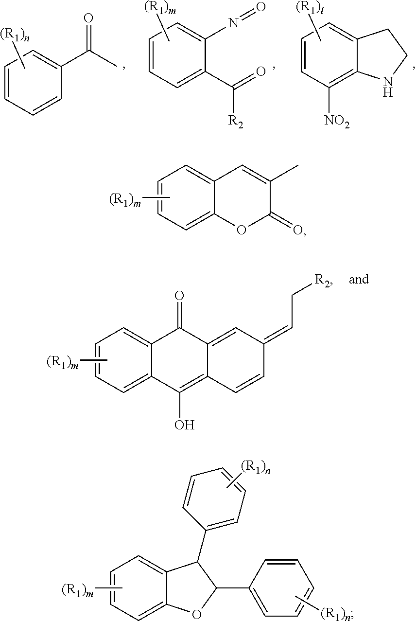
- the material of the residue layer preferably comprises: at least one compound selected from a group consisting of
- each R 1 independently is selected from a group consisting of C 1-6 alkyl, C 1-6 haloalkyl, C 1-6 alkoxy, —OH, —SH, —COOH, halogen, substituted C 1-6 alkyl, substituted C 1-6 alkoxy, C 2-6 alkenyl, —CN, —NO 2 , saturated or unsaturated 5 or 6-membered heterocyclic group containing at least one hetero atom, —N(R 5 ) 2 , and aryl, wherein the heterocyclic group or the aryl is selectively substituted or unsubstituted with a functional group; each R 2 independently is selected from a group consisting of hydrogen, C 1-6 alkyl, C 1-6 haloalkyl, C 1-6 alkoxy, —OH, —COOH, halogen, substituted C 1-6 alkyl, substituted C 1-6 alkoxy, C 2-6 alkenyl, —CN, —NO 2 , and aryl,
- each R 1 independently is selected from a group consisting of C 1-6 alkyl, C 1-6 alkoxy, —OH, —SH, —COOH, halogen, —NO 2 , and —N(R 5 ) 2
- each R 2 independently is selected from a group consisting of hydrogen, C 1-6 alkyl, C 1-6 haloalkyl, C 1-6 alkoxy, halogen, and —NO 2
- each R 5 independently is hydrogen or C 1-6 alkyl
- n is an integer ranging from 0 to 2
- 1 is an integer ranging from 0 to 2
- m is an integer ranging from 0 to 2.
- each R 1 independently is selected from a group consisting of C 1-4 alkyl, C 1-4 alkoxy, —OH, —SH, —COOH, halogen, —NO 2 , and —N(R 5 ) 2 ; each R 2 independently is selected from a group consisting of hydrogen, C 1-4 alkyl, C 1-4 fluoroalkyl, C 1-4 alkoxy, halogen, and —NO 2 ; each R 5 independently is hydrogen or C 1-4 alkyl; n is an integer ranging from 0 to 2; l is an integer ranging from 0 to 2; and m is an integer ranging from 0 to 2.
- examples of the R a of the compound represented by the formula (I) or (II) comprises, but not limited to: (wherein * represents the bonding site)
- the material of the residue layer is:
- each R 1 independently is selected from a group consisting of C 1-6 alkyl, C 1-6 alkoxy, —OH, —SH, —COOH, halogen, —NO 2 , and —N(R 5 ) 2 ; each R 5 independently is hydrogen or C 1-6 alkyl; and n is an integer ranging from 0 to 2.
- each R 1 independently is selected from a group consisting of C 1-4 alkyl, C 1-4 alkoxy, —OH, —COOH, —F, —Cl, —NO 2 , and —NH 2 ; and n is an integer ranging from 0 to 2.
- each R 1 independently is selected from a group consisting of methyl, ethyl, propyl, methoxy, ethyoxy, propoxy, —OH, —COOH, —F, —Cl, —NO 2 , and —NH 2 ; and n is 0 or 2.
- the R a of the compound represented by the formula (I) or (II), and the material of the residue layer obtained from the same respectively are:
- R a of the compound represented by the formula (I) or (II) is:
- the material of the residue layer is:
- each R 1 independently is selected from a group consisting of C 1-6 alkyl, C 1-6 alkoxy, —OH, —SH, —COOH, halogen, —NO 2 , and —N(R 5 ) 2 ; each R 5 independently is hydrogen or C 1-6 alkyl; and l is an integer ranging from 0 to 3.
- each R 1 independently is selected from a group consisting of C 1-4 alkyl, C 1-4 alkoxy, —OH, —SH, —COOH, —Cl, —Br, —NO 2 , and —NH 2 ; and l is an integer ranging from 0 to 2.
- each R 1 independently is selected from a group consisting of methyl, ethyl, propyl, methoxy, ethyoxy, propoxy, —OH, —COOH, —Cl, —Br, —NO 2 , and —NH 2 ; and l is an integer ranging from 0 to 2.
- the R a of the compound represented by the formula (I) or (II), and the material of the residue layer obtained from the same respectively are:
- R 1 is —Br or —NO 2 .
- R a of the compound represented by the formula (I) or (II) is:
- the material of the residue layer is:
- each R 1 independently is selected from a group consisting of C 1-6 alkyl, C 1-6 alkoxy, —OH, —SH, —COOH, halogen, —NO 2 , and —N(R 5 ) 2 ; each R 5 independently is hydrogen or C 1-6 alkyl; and m is an integer ranging from 0 to 4.
- each R 1 independently is selected from a group consisting of C 1-4 alkyl, C 1-4 alkoxy, —OH, —COOH, —F, —Cl, —NO 2 , and —N(R 5 ) 2 ; each R 5 independently is hydrogen or C 1-4 alkyl; and m is an integer ranging from 0 to 2.
- each R 1 independently is selected from a group consisting of methyl, ethyl, propyl, methoxy, ethyoxy, propoxy, —OH, —COOH, —Cl, and —N(R 5 ) 2 ; each R 5 independently is hydrogen, methyl, ethyl, or propyl; and m is an integer ranging from 0 to 2.
- the R a of the compound represented by the formula (I) or (II), and the material of the residue layer obtained from the same respectively are:
- both R 5 are hydrogen, methyl or ethyl in one molecule.
- R a of the compound represented by the formula (I) or (II) is:
- the material of the residue layer is:
- each R 1 independently is selected from a group consisting of C 1-6 alkyl, C 1-6 alkoxy, —OH, —SH, —COOH, halogen, —NO 2 , and —N(R 5 ) 2 ; each R 2 independently is selected from a group consisting of hydrogen, C 1-6 alkyl, C 1-6 haloalkyl, C 1-6 alkoxy, —OH, —COOH, halogen, —CN, and —NO 2 ; each R 5 independently is hydrogen or C 1-6 alkyl; and m is an integer ranging from 0 to 4.
- each R 1 independently is selected from a group consisting of C 1-4 alkyl, C 1-4 alkoxy, —OH, —SH, —COOH, —Cl, —Br, —NO 2 , and —N(R 5 ) 2 ; each R 2 independently is selected from a group consisting of hydrogen, C 1-4 alkyl, C 1-4 haloalkyl, C 1-4 alkoxy, —COOH, —Cl, —Br, —CN, and —NO 2 ; each R 5 independently is hydrogen or C 1-4 alkyl; and m is an integer ranging from 0 to 2.
- each R 1 independently is selected from a group consisting of methyl, ethyl, propyl, methoxy, ethyoxy, propoxy, —OH, —COOH, —Cl, —Br, —NO 2 , and —N(R 5 ) 2 ; each R 2 independently is selected from a group consisting of hydrogen, methyl, ethyl, propyl, methoxy, ethyoxy, propoxy, and —NO 2 ; each R 5 independently is hydrogen, methyl, ethyl, or propyl; and m is an integer ranging from 0 to 2.
- the R a of the compound represented by the formula (I) or (II), and the material of the residue layer obtained from the same respectively are:
- R a of the compound represented by the formula (I) or (II) is:
- the material of the residue layer is:
- each R 1 independently is selected from a group consisting of C 1-6 alkyl, C 1-6 alkoxy, —OH, —SH, —COOH, halogen, —NO 2 , and —N(R 5 ) 2 ; each R 5 independently is hydrogen or C 1-6 alkyl; n is an integer ranging from 0 to 5; and m is an integer ranging from 0 to 4.
- each R 1 independently is selected from a group consisting of C 1-4 alkyl, C 1-4 alkoxy, —OH, —COOH, —F, —NO 2 , and —NH 2 ; n and m are independently an integer ranging from 0 to 2.
- each R 1 independently is selected from a group consisting of methyl, ethyl, propyl, methoxy, ethyoxy, propoxy, —OH, —COOH, —F, —NO 2 , and —NH 2 ; n and m are independently 0 or 2.
- the R a of the compound represented by the formula (I) or (II), and the material of the residue layer obtained from the same respectively are:
- R a of the compound represented by the formula (I) or (II) is:
- the material of the residue layer is:
- each R 1 independently is selected from a group consisting of C 1-6 alkyl, C 1-6 haloalkyl, C 1-6 alkoxy, C 2-6 alkenyl, —OH, —SH, —COOH, halogen, —NO 2 , and —N(R 5 ) 2 ; each R 2 independently is selected from a group consisting of hydrogen, C 1-6 alkyl, C 1-6 haloalkyl, C 1-6 alkoxy, —OH, —COOH, halogen, —CN, and —NO 2 ; each R 5 independently is hydrogen or C 1-6 alkyl; and m is an integer ranging from 0 to 4.
- each R 1 independently is selected from a group consisting of C 1-4 alkyl, C 1-4 haloalkyl, C 1-4 alkoxy, —OH, —SH, —COOH, halogen, —NO 2 , and —N(R 5 ) 2 ; each R 2 independently is selected from a group consisting of hydrogen, C 1-6 alkyl, C 1-6 haloalkyl, C 1-6 alkoxy, —OH, —COOH, halogen, —CN, and —NO 2 ; each R 5 independently is hydrogen or C 1-4 alkyl; and m is an integer ranging from 0 to 4.
- each R 1 independently is selected from a group consisting of methyl, ethyl, propyl, methoxy, ethyoxy, propoxy, —CH 2 F, —CHF 2 , —CF 3 , —CH 2 Br, —CHBr 2 , —CBr 3 , —OH, —COOH, —F, —Cl, —Br, —NO 2 , and —N(R 5 ) 2 ; each R 2 independently is selected from a group consisting of hydrogen, methyl, ethyl, propyl, methoxy, ethyoxy, propoxy, —CH 2 F, —CHF 2 , —CF 3 , —CH 2 Br, —CHBr 2 , —CBr 3 , —OH, —F, —Cl, —Br, and —NO 2 ; each R 5 independently is hydrogen, methyl, ethyl, or propyl; and
- each R 1 independently is selected from a group consisting of methyl, ethyl, propyl, methoxy, ethyoxy, propoxy, —CH 2 F, —CHF 2 , —CF 3 , —OH, —COOH, —F, —Cl, —Br, —NO 2 , and —N(R 5 ) 2 ;
- each R 2 independently is selected from a group consisting of hydrogen, methyl, ethyl, propyl, methoxy, ethyoxy, propoxy, —CH 2 F, —CHF 2 , —CF 3 , —OH, —F, —Cl, —Br, and —NO 2 ; and each R 5 independently is hydrogen, methyl, ethyl, or propyl.
- Z 1 of the compound represented by the formula (I) or (II) is selected from a group consisting of O, S, N, C(R c ) 2 , and a bond;
- Z 2 is selected from a group consisting of O, S, and N;
- Z 3 is —HPO 3 — (—O—P( ⁇ O)(—OH)—) or —SO 3 — (—O—S( ⁇ O) 2 —); and
- p is an integer ranging from 1 to 5.
- each R c independently is hydrogen or C 1-6 alkyl.
- each R c independently is hydrogen or C 1-4 alkyl. More preferably, each R e independently is hydrogen, methyl, ethyl or propyl.
- R b of the compound represented by the formula (I) or (II) is —Si(OR d ) 3 or a polyimide chain represented by the following formula (III):
- each R d independently is hydrogen or C 1-6 alkyl.
- each R d independently is hydrogen or C 1-4 alkyl. More preferably, each R d independently is hydrogen, methyl, ethyl, or propyl. Most preferably, all R d in molecule are hydrogen, methyl, ethyl, or propyl at the same time.
- each R e independently is an aryl substituted or unsubstituted with a functional group. Preferably, each R e independently is an unsubstituted aryl group.
- q is an integer ranging from 50 to 500.
- q is an integer ranging from 50 to 100.
- the material of the debonding layer is the compound represented by the formula (I), wherein Z 1 is O, Z 2 is —N(H)—; R b is —Si(OR d ) 3 ; each R d independently is hydrogen or C 1-6 alkyl; p is an integer ranging from 1 to 5; and R a is:
- each R 1 independently is selected from a group consisting of methyl, ethyl, propyl, methoxy, ethyoxy, propoxy, —CH 2 F, —CHF 2 , —CF 3 , —OH, —COOH, —F, —Cl, —Br, —NO 2 , and —N(R 5 ) 2 ; each R 2 independently is selected from a group consisting of hydrogen, methyl, ethyl, propyl, methoxy, ethyoxy, propoxy, —CH 2 F, —CHF 2 , —CF 3 , —OH, —F, —Cl, —Br, and —NO 2 ; and each R 5 independently is hydrogen, methyl, ethyl, or propyl.
- all R d in one molecule are methyl, ethyl, propyl, or butyl; p is an integer ranging from 1 to 2; all R 1 in one molecule are methyl, ethyl, propyl, methoxy, ethyoxy, propoxy, —CH 2 F, —CHF 2 , —CF 3 , —OH, —COOH, —F, —Cl, —Br, —NO 2 , and —N(R 5 ) 2 ; each R 2 independently is selected from a group consisting of hydrogen, methyl, ethyl, and propyl; and each R 5 independently is hydrogen, methyl, or ethyl.
- the material of the residue layer in the obtained electronic apparatus is:
- each R 1 and R 2 are the same as the aforementioned definition.
- the term “unsubstituted or substituted” indicates that alkyl, haloalkyl, alkoxy, alkenyl, heterocyclic group, or aryl is unsubstituted or substituted with a functional group.
- this functional group preferably is a group capable of providing hydrophobicity, for example, epoxy, halogen such as F and Cl, thiol, —SH, and acyloxy.
- aryl used in the present invention includes aromatic rings containing 5, 6, 7, 8, 9 or more carbon atoms, and the examples thereof comprises but are not limited to: phenyl or naphthyl.
- the aryl is phenyl.
- alkyl used in the present invention includes linear and branch alkyl groups, and the examples thereof comprises but are not limited to: methyl, ethyl, n-propyl, isopropyl, n-butyl, iso-butyl, sec-butyl, tert-butyl, n-pentyl, iso-pentyl, and hexyl.
- halogen used in the present invention includes F, Cl, Br and I.
- the halogen used herein is F, Cl or Br. More preferably, the halogen used herein is Cl or Br.
- heterocyclic group used in the present invention indicates a heteroaryl group and a hetero-cycloalkyl group containing at least one hetero atom, each hetero atom is selected from 0, S and N, the ring of the heterocyclic group comprise 5 or 6 atoms, and any ring thereof does not contain two adjacent O or S.
- alkoxy used in the present invention indicates a group that an O atom is added onto the aforementioned alkyl, and the examples thereof comprise but are not limited to: methoxy, ethyoxy, propoxy, 2-propoxy, butoxy, iso-butoxy, pentyloxy, and hexyloxy.
- haloalkyl comprises alkyl, alkenyl, alkynyl, and alkoxy in which at least one hydrogen atom is substituted with a halogen atom; and when two or more hydrogen atoms are substituted with halogen atoms, these halogen atoms can be identical to or different from each other.
- the material of the carrier is not particularly limited, as long as the carrier can be applied on the current used machine in the art, for example, a glass carrier, a quartz carrier, or a plastic carrier.
- the carrier has a light transmittance larger than 30%. More preferably, the light transmittance of the carrier is in a range from 80% to 99%. Most preferably, the light transmittance thereof is in a range from 90% to 99%.
- the carrier preferably has a light transmittance larger than 30% under UV light radiation (which has a wavelength of 200-420 nm). More preferably the light transmittance of the carrier is in a range from 80% to 99% under UV light radiation. Most preferably, the light transmittance thereof is in a range from 90% to 99% under UV light radiation.
- the material of the debonding layer can be formed on the surface of the carrier through any known manner generally used in the art, such as dip coating, roll coating, print coating, spin coating, or deposition.
- the material of the debonding layer is preferably adhered on the carrier through covalent bonds.
- the concentration of the material in the mixture for forming the debonding layer is in a range from 0.01 wt % to 10 wt %.
- the concentration thereof is not limited to the aforementioned range, and can be adjusted according to the viscosity thereof and the used solvent in the mixture as long as the debonding layer can be formed uniformly on the substrate.
- the material of the debonding layer can be formed not only through the aforementioned manner, but also through chemical modification by directly bonding R b of the compound represented by the formula (I) or (II) onto the plastic substrate.
- the plastic carrier and the debonding layer together can be served as a plastic board.
- the thickness of the debonding layer is not particularly limited, as long as it can achieve the purpose of the present invention.
- the thickness thereof can be in a range from 100 ⁇ to 2000 ⁇ , but the present invention is not limited thereto.
- the substrate can be disposed on the carrier with the debonding layer formed thereon through any disposition manner generally used in the art, such as lamination and adhering process.
- the substrate can be formed on the carrier through coating a material for forming the substrate onto the carrier with the debonding layer formed thereon through the aforementioned coating manners, and then the substrate of the present invention can be obtained after a curing process.
- the debonding layer is located between the substrate and the carrier, and the second surface of the substrate contacts the debonding layer.
- the used substrate can be any flexible substrate generally used in the art.
- the flexible substrate has a feature that a bending displacement thereof is more than 80 mm.
- the “bending displacement” is defined by the following equation (I):
- ⁇ 5 32 ⁇ 1 4 ⁇ g ⁇ ⁇ ⁇ ⁇ ( 1 - v 2 ) Et 2 , ( I )
- ⁇ deformation amount
- ⁇ the gravity of the material
- l the length thereof
- ⁇ Poisson's ratio
- t the thickness thereof
- E Young's modulus
- g acceleration of gravity
- the examples of the flexible substrate capable of using in the present invention include: a thin glass substrate, a polymer substrate, a polymer-metal composite substrate, or a polymer-metal oxide composite substrate, in which the polymer can be PI, PA, PMMA, or a combination thereof, and the thin glass substrate is a glass substrate with a thickness of 0.1-0.3 mm.
- the electronic unit layer can be any unit known in the art, such as a display unit, a thin film transistor unit, and a touch unit, and one or a plurality of the aforementioned units can be laminated on the first surface of the substrate.
- the display unit is a liquid crystal display unit or an organic light emitting diode display unit.
- a radiation is performed on the debonding layer to photo-react (alternatively, photo-cleave) the material thereof, and thus the substrate can be separated from the carrier.
- the light absorbing group (R a ) of the material of the debonding layer is excited by an UV light source having wavelength ranging from 200 nm to 420 nm, the side product generated after the cleavage of the material thereof is remained on the second surface of the substrate to form a residue layer, wherein the residue layer may be adhered on the second surface of the substrate through a van der Waals' force, a hydrogen bond, or a ⁇ - ⁇ interaction.
- the radiation is provided from the side of the carrier, i.e. from the backside of the carrier. More specifically, in the method of the present invention, the radiation is provided onto the carrier without the debonding layer formed thereon, so that the light can be penetrated through the carrier to achieve the debonding layer to perform the photo-reaction (or, the photo-cleavage).
- the wavelength, the light intensity, and the radiation time are not particularly limited, and can be selected according to the material of the debonding layer, as long as the separation between the substrate and the carrier can be achieved.
- the wavelength of the UV light can be in a range from 200 nm to 420 nm; or the accumulated amount of the light can be in a range from 1 J to 60 J.
- FIG. 1A to FIG. 1E are cross-sectional views showing a process for manufacturing an electronic apparatus according to one preferred embodiment of the present invention.
- FIG. 1A to FIG. 1E the electronic apparatus and the method for manufacturing the same of one preferred embodiment of the present invention are illustrated in detail according to FIG. 1A to FIG. 1E .
- a carrier 11 which can be a glass carrier, a quartz carrier, or a plastic carrier known in the art, and has a light transmittance larger than 30%.
- a glass substrate or a plastic substrate having high light transmittance is used.
- a debonding layer 12 is formed on the carrier 11 through dip coating, roll coating, print coating, spin coating, or deposition, wherein the material of the debonding layer 12 comprises: a siloxane compound or a polyimide compound containing at least one selected from a group consisting of aryl, nitro and ketone.
- the specific examples of the material of the debonding layer 12 comprise: at least one compound represented by the following formula (I) or (II):
- each R 1 independently is selected from a group consisting of C 1-6 alkyl, C 1-6 haloalkyl, C 1-6 alkoxy, —OH, —SH, —COOH, halogen, substituted C 1-6 alkyl, substituted C 1-6 alkoxy, C 2-6 alkenyl, —CN, —NO 2 , saturated or unsaturated 5 or 6-membered heterocyclic group containing at least one hetero atom, —N(R 5 ) 2 , and aryl, wherein the heterocyclic group or the aryl is selectively substituted or unsubstituted with a functional group;
- each R 2 independently is selected from a group consisting of hydrogen, C 1-6 alkyl, C 1-6 haloalkyl, C 1-6 alkoxy, —OH, —COOH, halogen, substituted C 1-6 alkyl, substituted C 1-6 alkoxy, C 2-6 alkenyl, —CN, —NO 2 , and aryl, wherein the aryl is selectively substituted or unsubstituted with a functional group;
- each R 3 independently is selected from a group consisting of C 1-6 alkyl, C 1-6 haloalkyl, and aryl, wherein the aryl is selectively substituted or unsubstituted with a functional group;
- each R 4 independently is selected from a group consisting of C 1-6 alkyl, C 1-6 haloalkyl, halogen and —OH;
- each R 5 independently is hydrogen or C 1-6 alkyl
- X is O or S
- n is an integer ranging from 0 to 5;
- n is an integer ranging from 0 to 4.
- l is an integer ranging from 0 to 3;
- k is an integer ranging from 0 to 2;
- the material of the debonding layer 12 can be formed on the carrier 11 through covalent bonds.
- the carrier 11 used in the present embodiment is a plastic carrier
- the material of the debonding layer 12 can be bonded onto the carrier 11 through the R b of the compound represented by the formula (I) or (II) by chemical modification.
- the concentration of the material in the mixture for forming the debonding layer can be in a range from 0.01 wt % to 10 wt %, and the carrier 11 can be coated with the mixture through spin coating.
- the material of the debonding layer 12 can be directly formed on the carrier 11 through deposition.
- the thickness of the debonding layer 12 is not particularly limited, and can be in a range from 100 ⁇ to 2000 ⁇ . However, in other embodiment, the debonding layer 12 can have other thickness beyond the aforementioned range.
- the R a of the compound represented by the formula (I) or (II) can be selected from a group consisting of:
- each R 1 independently is selected from a group consisting of methyl, ethyl, propyl, methoxy, ethyoxy, propoxy, —CH 2 F, —CHF 2 , —CF 3 , —OH, —COOH, —F, —Cl, —Br, —NO 2 , and —N(R 5 ) 2 ; each R 2 independently is selected from a group consisting of hydrogen, methyl, ethyl, propyl, methoxy, ethyoxy, propoxy, —CH 2 F, —CHF 2 , —CF 3 , —OH, —F, —Cl, —Br, and —NO 2 ; and each R 5 independently is hydrogen, methyl, ethyl, or propyl.
- the material of the debonding layer 12 used in the present embodiment is:
- a substrate 13 is laminated on the debonding layer 12 to make the debonding layer 12 dispose between the carrier 11 and the substrate 13 , wherein the substrate 13 has a first surface 131 and a second surface 132 corresponding to each other, and the second surface 132 contacts the debonding layer 12 .
- the substrate 13 can be laminated on the carrier 11 with the debonding layer 12 formed thereon through any manner known in the art, such as lamination or adhering process.
- the material for forming the substrate 13 can be firstly formed on the carrier 11 with the debonding layer 12 by spin coating, and then a substrate 13 can be obtained after a curing process.
- the substrate 13 is preferably laminated on the carrier 11 with the debonding layer 12 through the adhering process.
- the substrate 13 can be any flexible substrate generally used in the art, and featured to have a bending displacement of more than 80 mm.
- the flexible substrate can be a thin glass substrate having a thickness in a range from 0.1 mm to 0.3 mm, a polymer substrate, a polymer-metal composite substrate, or a polymer-metal oxide composite substrate, wherein the polymer is PI, PA, PMMA, or a combination thereof.
- an electronic unit layer 14 is formed on the substrate 13 through a known process used in the art.
- the electronic unit layer 14 can comprise the electronic units generally used in the art, such as a display unit, a thin film transistor unit, and a touch unit, and the aforementioned electronic units can be used alone or together to form the electronic unit layer 14 .
- the known display unit in the art can be a liquid crystal display unit or an organic light emitting diode display unit.
- a radiation is performed on a side of the carrier 11 to react the material of the debonding layer 12 to separate the substrate 13 from the carrier.
- an electronic apparatus is obtained, as shown in FIG. 1E .
- the radiation is provided from the backside of the carrier 11 .
- the radiation is provided from the carrier 11 without the debonding layer 12 formed thereon, and the light penetrates through the carrier 11 and achieves the debonding layer 12 to perform a photo-reaction (or, photo-cleavage) on the material thereof.
- the substrate 13 can be separated from the carrier, as shown in FIG. 1E .
- the light absorbing group (R a ) of the material of the debonding layer 12 is excited to perform the cleavage reaction, and the generated derivative after the cleavage reaction is remained on the second surface 132 of the substrate 13 to form a residue layer 121 , wherein the residue layer 121 is disposed on the second surface 132 of the substrate 13 through a van der Waals' force, a hydrogen bond, or a ⁇ - ⁇ interaction.
- the wavelength, the light intensity, and the radiation time can be selected according to the material of the debonding layer 12 .
- the wavelength of the UV light can be in a range from 200 nm to 420 nm, and the accumulated amount of the light can be in a range from 1 J to 60 J.
- the radiation conditions used in the other embodiments of the present invention are not limited to the aforementioned ranges. Therefore, the material of the obtained residue layer comprises: a compound containing at least one selected from a group consisting of aryl, nitro and ketone; and comprises: at least one derivative of a material represented by the aforementioned formula (I) or (II) obtained after a radiation.
- the material of the residue layer 121 of the present embodiment comprises: at least one compound selected from a group consisting of:
- each R 1 independently is selected from a group consisting of methyl, ethyl, propyl, methoxy, ethyoxy, propoxy, —CH 2 F, —CHF 2 , —CF 3 , —OH, —COOH, —F, —Cl, —Br, —NO 2 , and —N(R 5 ) 2 ; each R 2 independently is selected from a group consisting of hydrogen, methyl, ethyl, propyl, methoxy, ethyoxy, propoxy, —CH 2 F, —CHF 2 , —CF 3 , —OH, —F, —Cl, —Br, and —NO 2 ; and each R 5 independently is hydrogen, methyl, ethyl, or propyl.
- the material of the residue layer 121 obtained in the present embodiment is:
- the electronic apparatus of the present embodiment comprises: a substrate 13 with a first surface 131 and a second surface 132 corresponding to each other; an electronic unit layer 14 disposed on the first surface 131 of the substrate 13 ; and a residue layer 121 disposed on the second surface 132 of the substrate 13 , wherein a material of the residue layer 121 comprises: at least one derivative of a material represented by the aforementioned formula (I) or (II) obtained after a radiation.
- the electronic apparatus obtained in the present embodiment can also be applied to various display panels, such as liquid crystal display (LED) panel or organic light emitting diode display (OLED) panel.
- the obtained display panel can further be applied to various electronic devices, such as cell phones, notebooks, video cameras, cameras, music players, navigation devices, and televisions.
Landscapes
- Engineering & Computer Science (AREA)
- Microelectronics & Electronic Packaging (AREA)
- Manufacturing & Machinery (AREA)
- Electroluminescent Light Sources (AREA)
- Laminated Bodies (AREA)
- Thin Film Transistor (AREA)
- Chemical & Material Sciences (AREA)
- Ceramic Engineering (AREA)
- Inorganic Chemistry (AREA)
Abstract
Description

- wherein Z1 is selected from a group consisting of O, S, N, C(Rc)2, and a bond;
- Z2 is selected from a group consisting of O, S, and N(H);
- Z3 is HPO3 or SO3;
- Ra is selected from a group consisting of:


- Rb is —Si(ORd)3, or

- each Rc independently is hydrogen or C1-6 alkyl;
- each Rd independently is hydrogen or C1-6 alkyl;
- each Re independently is an aryl substituted or unsubstituted with a functional group;
- p is an integer ranging from 1 to 5; and
- q is an integer ranging from 50 to 500.


wherein each R1 independently is selected from a group consisting of C1-6 alkyl, C1-6 haloalkyl, C1-6 alkoxy, —OH, —SH, —COOH, halogen, substituted C1-6 alkyl, substituted C1-6 alkoxy, C2-6 alkenyl, —CN, —NO2, saturated or unsaturated 5 or 6-membered heterocyclic group containing at least one hetero atom, —N(R5)2, and aryl, wherein the heterocyclic group or the aryl is selectively substituted or unsubstituted with a functional group; each R2 independently is selected from a group consisting of hydrogen, C1-6 alkyl, C1-6 haloalkyl, C1-6 alkoxy, —OH, —COOH, halogen, substituted C1-6 alkyl, substituted C1-6 alkoxy, C2-6 alkenyl, —CN, —NO2, and aryl, wherein the aryl is selectively unsubstituted or substituted with a functional group; each R5 independently is hydrogen or C1-6 alkyl; n is an integer ranging from 0 to 5; m is an integer ranging from 0 to 4; and l is an integer ranging from 0 to 3.


Therefore, in the electronic apparatus obtained by the method of the present aspect, the material of the residue layer is:

Herein, each R1 independently is selected from a group consisting of C1-6 alkyl, C1-6 alkoxy, —OH, —SH, —COOH, halogen, —NO2, and —N(R5)2; each R5 independently is hydrogen or C1-6 alkyl; and n is an integer ranging from 0 to 2. Preferably, each R1 independently is selected from a group consisting of C1-4 alkyl, C1-4 alkoxy, —OH, —COOH, —F, —Cl, —NO2, and —NH2; and n is an integer ranging from 0 to 2. More preferably, each R1 independently is selected from a group consisting of methyl, ethyl, propyl, methoxy, ethyoxy, propoxy, —OH, —COOH, —F, —Cl, —NO2, and —NH2; and n is 0 or 2. Most preferably, the Ra of the compound represented by the formula (I) or (II), and the material of the residue layer obtained from the same respectively are:


Therefore, in the electronic apparatus obtained by the method of the present aspect, the material of the residue layer is:

Herein, each R1 independently is selected from a group consisting of C1-6 alkyl, C1-6 alkoxy, —OH, —SH, —COOH, halogen, —NO2, and —N(R5)2; each R5 independently is hydrogen or C1-6 alkyl; and l is an integer ranging from 0 to 3. Preferably, each R1 independently is selected from a group consisting of C1-4 alkyl, C1-4 alkoxy, —OH, —SH, —COOH, —Cl, —Br, —NO2, and —NH2; and l is an integer ranging from 0 to 2. More preferably, each R1 independently is selected from a group consisting of methyl, ethyl, propyl, methoxy, ethyoxy, propoxy, —OH, —COOH, —Cl, —Br, —NO2, and —NH2; and l is an integer ranging from 0 to 2. Most preferably, the Ra of the compound represented by the formula (I) or (II), and the material of the residue layer obtained from the same respectively are:

wherein, R1 is —Br or —NO2.

Therefore, in the electronic apparatus obtained by the method of the present aspect, the material of the residue layer is:
Herein, each R1 independently is selected from a group consisting of C1-6 alkyl, C1-6 alkoxy, —OH, —SH, —COOH, halogen, —NO2, and —N(R5)2; each R5 independently is hydrogen or C1-6 alkyl; and m is an integer ranging from 0 to 4. Preferably, each R1 independently is selected from a group consisting of C1-4 alkyl, C1-4 alkoxy, —OH, —COOH, —F, —Cl, —NO2, and —N(R5)2; each R5 independently is hydrogen or C1-4 alkyl; and m is an integer ranging from 0 to 2. More preferably, each R1 independently is selected from a group consisting of methyl, ethyl, propyl, methoxy, ethyoxy, propoxy, —OH, —COOH, —Cl, and —N(R5)2; each R5 independently is hydrogen, methyl, ethyl, or propyl; and m is an integer ranging from 0 to 2. Most preferably, the Ra of the compound represented by the formula (I) or (II), and the material of the residue layer obtained from the same respectively are:

wherein, both R5 are hydrogen, methyl or ethyl in one molecule.

Therefore, in the electronic apparatus obtained by the method of the present aspect, the material of the residue layer is:

Herein, each R1 independently is selected from a group consisting of C1-6 alkyl, C1-6 alkoxy, —OH, —SH, —COOH, halogen, —NO2, and —N(R5)2; each R2 independently is selected from a group consisting of hydrogen, C1-6 alkyl, C1-6 haloalkyl, C1-6 alkoxy, —OH, —COOH, halogen, —CN, and —NO2; each R5 independently is hydrogen or C1-6 alkyl; and m is an integer ranging from 0 to 4. Preferably, each R1 independently is selected from a group consisting of C1-4 alkyl, C1-4 alkoxy, —OH, —SH, —COOH, —Cl, —Br, —NO2, and —N(R5)2; each R2 independently is selected from a group consisting of hydrogen, C1-4 alkyl, C1-4 haloalkyl, C1-4 alkoxy, —COOH, —Cl, —Br, —CN, and —NO2; each R5 independently is hydrogen or C1-4 alkyl; and m is an integer ranging from 0 to 2. More preferably, each R1 independently is selected from a group consisting of methyl, ethyl, propyl, methoxy, ethyoxy, propoxy, —OH, —COOH, —Cl, —Br, —NO2, and —N(R5)2; each R2 independently is selected from a group consisting of hydrogen, methyl, ethyl, propyl, methoxy, ethyoxy, propoxy, and —NO2; each R5 independently is hydrogen, methyl, ethyl, or propyl; and m is an integer ranging from 0 to 2. Most preferably, the Ra of the compound represented by the formula (I) or (II), and the material of the residue layer obtained from the same respectively are:


Therefore, in the electronic apparatus obtained by the method of the present aspect, the material of the residue layer is:

Herein, each R1 independently is selected from a group consisting of C1-6 alkyl, C1-6 alkoxy, —OH, —SH, —COOH, halogen, —NO2, and —N(R5)2; each R5 independently is hydrogen or C1-6 alkyl; n is an integer ranging from 0 to 5; and m is an integer ranging from 0 to 4. Preferably, each R1 independently is selected from a group consisting of C1-4 alkyl, C1-4 alkoxy, —OH, —COOH, —F, —NO2, and —NH2; n and m are independently an integer ranging from 0 to 2. More preferably, each R1 independently is selected from a group consisting of methyl, ethyl, propyl, methoxy, ethyoxy, propoxy, —OH, —COOH, —F, —NO2, and —NH2; n and m are independently 0 or 2. Most preferably, the Ra of the compound represented by the formula (I) or (II), and the material of the residue layer obtained from the same respectively are:


Therefore, in the electronic apparatus obtained by the method of the present aspect, the material of the residue layer is:

Herein, each R1 independently is selected from a group consisting of C1-6 alkyl, C1-6 haloalkyl, C1-6 alkoxy, C2-6 alkenyl, —OH, —SH, —COOH, halogen, —NO2, and —N(R5)2; each R2 independently is selected from a group consisting of hydrogen, C1-6 alkyl, C1-6 haloalkyl, C1-6 alkoxy, —OH, —COOH, halogen, —CN, and —NO2; each R5 independently is hydrogen or C1-6 alkyl; and m is an integer ranging from 0 to 4. Preferably, each R1 independently is selected from a group consisting of C1-4 alkyl, C1-4 haloalkyl, C1-4 alkoxy, —OH, —SH, —COOH, halogen, —NO2, and —N(R5)2; each R2 independently is selected from a group consisting of hydrogen, C1-6 alkyl, C1-6 haloalkyl, C1-6 alkoxy, —OH, —COOH, halogen, —CN, and —NO2; each R5 independently is hydrogen or C1-4 alkyl; and m is an integer ranging from 0 to 4. More preferably, each R1 independently is selected from a group consisting of methyl, ethyl, propyl, methoxy, ethyoxy, propoxy, —CH2F, —CHF2, —CF3, —CH2Br, —CHBr2, —CBr3, —OH, —COOH, —F, —Cl, —Br, —NO2, and —N(R5)2; each R2 independently is selected from a group consisting of hydrogen, methyl, ethyl, propyl, methoxy, ethyoxy, propoxy, —CH2F, —CHF2, —CF3, —CH2Br, —CHBr2, —CBr3, —OH, —F, —Cl, —Br, and —NO2; each R5 independently is hydrogen, methyl, ethyl, or propyl; and m is an integer ranging from 0 to 2. Most preferably, the Ra of the compound represented by the formula (I) or (II), and the material of the residue layer obtained from the same respectively are:

Herein, each R1 independently is selected from a group consisting of methyl, ethyl, propyl, methoxy, ethyoxy, propoxy, —CH2F, —CHF2, —CF3, —OH, —COOH, —F, —Cl, —Br, —NO2, and —N(R5)2; each R2 independently is selected from a group consisting of hydrogen, methyl, ethyl, propyl, methoxy, ethyoxy, propoxy, —CH2F, —CHF2, —CF3, —OH, —F, —Cl, —Br, and —NO2; and each R5 independently is hydrogen, methyl, ethyl, or propyl.

Herein, each Rd independently is hydrogen or C1-6 alkyl. Preferably, each Rd independently is hydrogen or C1-4 alkyl. More preferably, each Rd independently is hydrogen, methyl, ethyl, or propyl. Most preferably, all Rd in molecule are hydrogen, methyl, ethyl, or propyl at the same time. In addition, each Re independently is an aryl substituted or unsubstituted with a functional group. Preferably, each Re independently is an unsubstituted aryl group. Furthermore, q is an integer ranging from 50 to 500. Preferably, q is an integer ranging from 50 to 100.

wherein each R1 independently is selected from a group consisting of methyl, ethyl, propyl, methoxy, ethyoxy, propoxy, —CH2F, —CHF2, —CF3, —OH, —COOH, —F, —Cl, —Br, —NO2, and —N(R5)2; each R2 independently is selected from a group consisting of hydrogen, methyl, ethyl, propyl, methoxy, ethyoxy, propoxy, —CH2F, —CHF2, —CF3, —OH, —F, —Cl, —Br, and —NO2; and each R5 independently is hydrogen, methyl, ethyl, or propyl. Preferably, all Rd in one molecule are methyl, ethyl, propyl, or butyl; p is an integer ranging from 1 to 2; all R1 in one molecule are methyl, ethyl, propyl, methoxy, ethyoxy, propoxy, —CH2F, —CHF2, —CF3, —OH, —COOH, —F, —Cl, —Br, —NO2, and —N(R5)2; each R2 independently is selected from a group consisting of hydrogen, methyl, ethyl, and propyl; and each R5 independently is hydrogen, methyl, or ethyl. Thus, in the most preferred embodiment of the present invention, the material of the residue layer in the obtained electronic apparatus is:

wherein each R1 and R2 are the same as the aforementioned definition.
wherein ω is deformation amount, ρ is the gravity of the material, l is the length thereof, ν is Poisson's ratio, t is the thickness thereof, E is Young's modulus, and g is acceleration of gravity.

- wherein Z1 is selected from a group consisting of O, S, N, C(Rc)2, and a bond;
- Z2 is selected from a group consisting of O, S, and N;
- Z3 is HPO3 or SO3;
- Ra is selected from a group consisting of:


- Rb is —Si(ORd)3, or

- each Rc independently is hydrogen or C1-6 alkyl;
- each Rd independently is hydrogen or C1-6 alkyl;
- each Re independently is an aryl substituted or unsubstituted with a functional group;
- p is an integer ranging from 1 to 5; and
- q is an integer ranging from 50 to 500.

wherein each R1 independently is selected from a group consisting of methyl, ethyl, propyl, methoxy, ethyoxy, propoxy, —CH2F, —CHF2, —CF3, —OH, —COOH, —F, —Cl, —Br, —NO2, and —N(R5)2; each R2 independently is selected from a group consisting of hydrogen, methyl, ethyl, propyl, methoxy, ethyoxy, propoxy, —CH2F, —CHF2, —CF3, —OH, —F, —Cl, —Br, and —NO2; and each R5 independently is hydrogen, methyl, ethyl, or propyl.

but the present invention is not particularly limited to this compound in other embodiments.
Claims (18)


Applications Claiming Priority (6)
| Application Number | Priority Date | Filing Date | Title |
|---|---|---|---|
| TW102120101 | 2013-06-06 | ||
| TW102120101 | 2013-06-06 | ||
| TW102120101A | 2013-06-06 | ||
| TW103106686A TWI542261B (en) | 2013-06-06 | 2014-02-27 | Electronic apparatus and method for manufacturing the same |
| TW103106686 | 2014-02-27 | ||
| TW103106686A | 2014-02-27 |
Publications (2)
| Publication Number | Publication Date |
|---|---|
| US20140362545A1 US20140362545A1 (en) | 2014-12-11 |
| US9832880B2 true US9832880B2 (en) | 2017-11-28 |
Family
ID=52005313
Family Applications (1)
| Application Number | Title | Priority Date | Filing Date |
|---|---|---|---|
| US14/279,792 Active 2035-11-11 US9832880B2 (en) | 2013-06-06 | 2014-05-16 | Electronic apparatus and method for manufacturing the same |
Country Status (3)
| Country | Link |
|---|---|
| US (1) | US9832880B2 (en) |
| CN (1) | CN104241322B (en) |
| TW (1) | TWI542261B (en) |
Cited By (1)
| Publication number | Priority date | Publication date | Assignee | Title |
|---|---|---|---|---|
| US12525572B2 (en) | 2021-03-31 | 2026-01-13 | Adeia Semiconductor Bonding Technologies Inc. | Direct bonding and debonding of carrier |
Families Citing this family (2)
| Publication number | Priority date | Publication date | Assignee | Title |
|---|---|---|---|---|
| CN105374829B (en) * | 2015-12-01 | 2018-03-27 | 上海天马有机发光显示技术有限公司 | A kind of flexible display substrates and preparation method thereof |
| CN105489789B (en) * | 2016-01-18 | 2017-03-01 | 京东方科技集团股份有限公司 | Manufacturing method of flexible device and flexible display device |
Citations (4)
| Publication number | Priority date | Publication date | Assignee | Title |
|---|---|---|---|---|
| JP2000243943A (en) * | 1999-02-23 | 2000-09-08 | Seiko Epson Corp | Method for manufacturing semiconductor device |
| TW200540474A (en) | 2004-05-04 | 2005-12-16 | Eastman Kodak Co | Polarizing plate laminated with improved glue composition |
| CN102468452A (en) | 2010-11-11 | 2012-05-23 | 乐金显示有限公司 | Method for manufacturing flexible flat device |
| TW201235738A (en) | 2011-02-25 | 2012-09-01 | Chimei Innolux Corp | Display and method for manufacturing the same |
Family Cites Families (2)
| Publication number | Priority date | Publication date | Assignee | Title |
|---|---|---|---|---|
| KR101328275B1 (en) * | 2010-09-29 | 2013-11-14 | 주식회사 포스코 | Chemical peel-off method of manufacturing flexible electronic device, flexible electronic device and flexible substrate |
| CN102738078B (en) * | 2012-06-21 | 2014-11-12 | 京东方科技集团股份有限公司 | Method for manufacturing flexible display substrate |
-
2014
- 2014-02-27 TW TW103106686A patent/TWI542261B/en not_active IP Right Cessation
- 2014-05-06 CN CN201410188251.7A patent/CN104241322B/en active Active
- 2014-05-16 US US14/279,792 patent/US9832880B2/en active Active
Patent Citations (4)
| Publication number | Priority date | Publication date | Assignee | Title |
|---|---|---|---|---|
| JP2000243943A (en) * | 1999-02-23 | 2000-09-08 | Seiko Epson Corp | Method for manufacturing semiconductor device |
| TW200540474A (en) | 2004-05-04 | 2005-12-16 | Eastman Kodak Co | Polarizing plate laminated with improved glue composition |
| CN102468452A (en) | 2010-11-11 | 2012-05-23 | 乐金显示有限公司 | Method for manufacturing flexible flat device |
| TW201235738A (en) | 2011-02-25 | 2012-09-01 | Chimei Innolux Corp | Display and method for manufacturing the same |
Non-Patent Citations (1)
| Title |
|---|
| Machine translation of JP 2000-243943A, Sep. 2000. * |
Cited By (1)
| Publication number | Priority date | Publication date | Assignee | Title |
|---|---|---|---|---|
| US12525572B2 (en) | 2021-03-31 | 2026-01-13 | Adeia Semiconductor Bonding Technologies Inc. | Direct bonding and debonding of carrier |
Also Published As
| Publication number | Publication date |
|---|---|
| US20140362545A1 (en) | 2014-12-11 |
| CN104241322A (en) | 2014-12-24 |
| TWI542261B (en) | 2016-07-11 |
| CN104241322B (en) | 2017-06-13 |
| TW201448683A (en) | 2014-12-16 |
Similar Documents
| Publication | Publication Date | Title |
|---|---|---|
| TWI488750B (en) | Method and assembly for reducing warpage and bending of a flexible substrate in a semiconductor process | |
| CN102468452B (en) | Method for manufacturing flexible flat device | |
| CN101300899B (en) | Method for preparing device with flexible substrate and device with flexible substrate prepared by the method | |
| US9832880B2 (en) | Electronic apparatus and method for manufacturing the same | |
| CN107302014A (en) | A kind of organic electroluminescence display panel, its display device and preparation method thereof | |
| US20130040124A1 (en) | Method for preparing transparent antistatic films using graphene and transparent antistatic films prepared by the same | |
| CN103151306A (en) | Method for manufacturing flexible electronic device | |
| JP2009530441A5 (en) | ||
| TW201117956A (en) | Laminated glass substrate, process for production of the laminated glass substrate, and electronic device equipped with the laminated glass substrate | |
| RU2005129845A (en) | SYSTEM AND METHOD FOR PROTECTING AN ARRAY OF MICROELECTROMECHANICAL SYSTEMS USING A STRUCTURALLY REINFORCED REAR PLATE | |
| RU2009125008A (en) | REMOVABLE ADHESIVE TAPE | |
| TW200624254A (en) | Process for production of substrates having water-repellent hydrophilic films on the surface | |
| JP2014212107A (en) | Organic electroluminescent device and method of manufacturing the same | |
| TW200739146A (en) | Method for producing complex phase retarder and complex optical member | |
| JP6443850B2 (en) | Nanoimprinting composition, member manufacturing method, and device manufacturing method | |
| US8790149B2 (en) | Method of fabricating flexible display device | |
| US20190027458A1 (en) | Method for manufacturing electronic device | |
| KR101696965B1 (en) | Photocurable composition and encapsulated apparatus comprising the same | |
| TW200638791A (en) | Method for producing flexible organic electro-luminescent faceplate and display module thereof | |
| US9748516B2 (en) | Functional film | |
| TW200720718A (en) | Process for producing optical film | |
| KR20140144528A (en) | Polyimide precursor composition | |
| US20130321996A1 (en) | Production method for a bezel for a display panel using mould casting, and bezel for a display panel produced thereby | |
| KR20150062668A (en) | Material for sacrificial layer and method for preparing flexible display using the same | |
| US20170084838A1 (en) | Electronic device and method for manufacturing the same |
Legal Events
| Date | Code | Title | Description |
|---|---|---|---|
| AS | Assignment |
Owner name: INNOLUX CORPORATION, TAIWAN Free format text: ASSIGNMENT OF ASSIGNORS INTEREST;ASSIGNORS:TSAI, CHI-CHE;CHEN, YU-YAO;HSU, PO-YUN;AND OTHERS;REEL/FRAME:032914/0290 Effective date: 20140514 |
|
| STCF | Information on status: patent grant |
Free format text: PATENTED CASE |
|
| MAFP | Maintenance fee payment |
Free format text: PAYMENT OF MAINTENANCE FEE, 4TH YEAR, LARGE ENTITY (ORIGINAL EVENT CODE: M1551); ENTITY STATUS OF PATENT OWNER: LARGE ENTITY Year of fee payment: 4 |
|
| MAFP | Maintenance fee payment |
Free format text: PAYMENT OF MAINTENANCE FEE, 8TH YEAR, LARGE ENTITY (ORIGINAL EVENT CODE: M1552); ENTITY STATUS OF PATENT OWNER: LARGE ENTITY Year of fee payment: 8 |