US9832050B1 - Shock sensor resonance detection for notch filter tuning - Google Patents
Shock sensor resonance detection for notch filter tuning Download PDFInfo
- Publication number
- US9832050B1 US9832050B1 US15/354,867 US201615354867A US9832050B1 US 9832050 B1 US9832050 B1 US 9832050B1 US 201615354867 A US201615354867 A US 201615354867A US 9832050 B1 US9832050 B1 US 9832050B1
- Authority
- US
- United States
- Prior art keywords
- frequency
- notch filter
- detection system
- shock detection
- output signal
- Prior art date
- Legal status (The legal status is an assumption and is not a legal conclusion. Google has not performed a legal analysis and makes no representation as to the accuracy of the status listed.)
- Active
Links
Images


Classifications
-
- H—ELECTRICITY
- H04—ELECTRIC COMMUNICATION TECHNIQUE
- H04L—TRANSMISSION OF DIGITAL INFORMATION, e.g. TELEGRAPHIC COMMUNICATION
- H04L25/00—Baseband systems
- H04L25/38—Synchronous or start-stop systems, e.g. for Baudot code
- H04L25/40—Transmitting circuits; Receiving circuits
- H04L25/49—Transmitting circuits; Receiving circuits using code conversion at the transmitter; using predistortion; using insertion of idle bits for obtaining a desired frequency spectrum; using three or more amplitude levels ; Baseband coding techniques specific to data transmission systems
- H04L25/4902—Pulse width modulation; Pulse position modulation
-
- G—PHYSICS
- G01—MEASURING; TESTING
- G01P—MEASURING LINEAR OR ANGULAR SPEED, ACCELERATION, DECELERATION, OR SHOCK; INDICATING PRESENCE, ABSENCE, OR DIRECTION, OF MOVEMENT
- G01P15/00—Measuring acceleration; Measuring deceleration; Measuring shock, i.e. sudden change of acceleration
- G01P15/02—Measuring acceleration; Measuring deceleration; Measuring shock, i.e. sudden change of acceleration by making use of inertia forces using solid seismic masses
- G01P15/08—Measuring acceleration; Measuring deceleration; Measuring shock, i.e. sudden change of acceleration by making use of inertia forces using solid seismic masses with conversion into electric or magnetic values
- G01P15/0802—Details
-
- G—PHYSICS
- G01—MEASURING; TESTING
- G01P—MEASURING LINEAR OR ANGULAR SPEED, ACCELERATION, DECELERATION, OR SHOCK; INDICATING PRESENCE, ABSENCE, OR DIRECTION, OF MOVEMENT
- G01P15/00—Measuring acceleration; Measuring deceleration; Measuring shock, i.e. sudden change of acceleration
- G01P15/02—Measuring acceleration; Measuring deceleration; Measuring shock, i.e. sudden change of acceleration by making use of inertia forces using solid seismic masses
- G01P15/08—Measuring acceleration; Measuring deceleration; Measuring shock, i.e. sudden change of acceleration by making use of inertia forces using solid seismic masses with conversion into electric or magnetic values
- G01P15/0891—Measuring acceleration; Measuring deceleration; Measuring shock, i.e. sudden change of acceleration by making use of inertia forces using solid seismic masses with conversion into electric or magnetic values with indication of predetermined acceleration values
-
- G—PHYSICS
- G11—INFORMATION STORAGE
- G11B—INFORMATION STORAGE BASED ON RELATIVE MOVEMENT BETWEEN RECORD CARRIER AND TRANSDUCER
- G11B19/00—Driving, starting, stopping record carriers not specifically of filamentary or web form, or of supports therefor; Control thereof; Control of operating function ; Driving both disc and head
- G11B19/02—Control of operating function, e.g. switching from recording to reproducing
- G11B19/04—Arrangements for preventing, inhibiting, or warning against double recording on the same blank or against other recording or reproducing malfunctions
- G11B19/041—Detection or prevention of read or write errors
- G11B19/042—Detection or prevention of read or write errors due to external shock or vibration
-
- G—PHYSICS
- G11—INFORMATION STORAGE
- G11B—INFORMATION STORAGE BASED ON RELATIVE MOVEMENT BETWEEN RECORD CARRIER AND TRANSDUCER
- G11B19/00—Driving, starting, stopping record carriers not specifically of filamentary or web form, or of supports therefor; Control thereof; Control of operating function ; Driving both disc and head
- G11B19/20—Driving; Starting; Stopping; Control thereof
- G11B19/28—Speed controlling, regulating, or indicating
-
- G—PHYSICS
- G11—INFORMATION STORAGE
- G11B—INFORMATION STORAGE BASED ON RELATIVE MOVEMENT BETWEEN RECORD CARRIER AND TRANSDUCER
- G11B5/00—Recording by magnetisation or demagnetisation of a record carrier; Reproducing by magnetic means; Record carriers therefor
- G11B5/48—Disposition or mounting of heads or head supports relative to record carriers ; arrangements of heads, e.g. for scanning the record carrier to increase the relative speed
- G11B5/54—Disposition or mounting of heads or head supports relative to record carriers ; arrangements of heads, e.g. for scanning the record carrier to increase the relative speed with provision for moving the head into or out of its operative position or across tracks
- G11B5/55—Track change, selection or acquisition by displacement of the head
- G11B5/5521—Track change, selection or acquisition by displacement of the head across disk tracks
- G11B5/5582—Track change, selection or acquisition by displacement of the head across disk tracks system adaptation for working during or after external perturbation, e.g. in the presence of a mechanical oscillation caused by a shock
Definitions
- a conventional shock sensor used in a data storage device for example a hard disk drive (HDD), to detect mechanical shocks and prevent off-track writes (OTWs) may be designed as a cantilever beam structure with piezoelectric properties.
- a shock event causes the beam to deflect producing a small electric charge.
- the small electric charge produced by the shock sensor is amplified and filtered by a shock detection system and the output of the shock detection system is compared to a predetermined voltage threshold to determine whether the detected shock is large enough to require suspension of write operations.
- an interrupt signal is issued to the system-on-a-chip (SoC), which immediately suspends write operations to prevent overwriting data on adjoining tracks.
- SoC system-on-a-chip
- FIG. 1 is a diagram illustrating a DSD 100 including a conventional shock detection system.
- the DSD 100 may include a disk 110 rotated by a spindle 115 coupled to a spindle motor 120 and a head 125 connected to an end of an actuator arm 130 which is rotated about a pivot by a voice coil motor (VCM) 135 to position the head 125 radially over the disk 110 .
- the VCM 135 may controlled by a VCM drive signal 157 from a VCM control circuit 155 .
- the disk may include a number of concentric data tracks each partitioned into a number of data sectors.
- the spindle motor 120 may be driven by a spindle drive signal 142 generated by a pulse width modulator (PWM) 140 .
- a control unit 150 may control the PWM 140 and the VCM control circuit 155 and may receive input from a shock detection system 160 .
- FIG. 2A is a simplified block diagram of a shock detection system in accordance with various aspects of the present disclosure.
- the shock detection system 160 may include a shock sensor 165 , a first gain stage (e.g., a charge amplifier) 170 , a notch filter 175 , additional circuitry including filters 180 , for example, but not limited to, firmware tunable filters, and gain stages 185 , and one or more window comparators 190 .
- the shock detection system 160 may be configured to generate an interrupt signal to the control unit 150 upon detection of a mechanical shock exceeding a threshold.
- the mechanical response of the shock sensor 165 may be that of a second-order mechanical system with a pronounced resonance, usually with a Q-factor on the order of 50.
- a notch filter 175 may be used as part of the shock detection system 160 to suppress the resonance of the shock sensor 165 while minimizing the phase delay of the shock detection system 160 at lower frequencies to provide rapid detection of shock events.
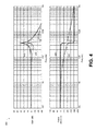
- FIG. 3 is a graph 300 illustrating example gain and phase plots of the shock detection system before and after application of a conventional fixed notch filter for a shock detection system output signal 162 .
- the example gain 310 and phase 320 plots of the shock detection system without a notch filter and the example gain 330 and phase 340 plots of the shock detection system output signal 162 after application of a conventional notch filter with a Q-factor of 1.0 when frequency of the notch filter (f notch ) is equal to the resonance frequency of the shock sensor (f sensor ) are shown.
- maximum gain and minimal phase delay is required up to about 20 kHz.
- a notch filter Q-factor of 1.0 sufficiently suppresses the resonance frequency of the sensor while maintaining a flat output magnitude and minimizing the phase loss.
- FIG. 4 is a graph 400 illustrating example gain and phase plots before and after application of a conventional fixed notch filter for a shock detection system output signal 162 .
- example gain 410 and phase 420 plots of the shock detection system output signal 162 without a notch filter
- example gain 430 and phase 440 plots of the shock detection system output after a conventional notch filter with a Q-factor of 0.25 when frequency of the notch filter (f notch ) is not equal to the resonance frequency of the shock sensor (f sensor ) are shown.
- the specified resonance frequency range of a typical shock sensor may be 44 ⁇ 8 kHz. With this wide range of part-to-part variation in resonance frequency (and without resonance detection), the Q-factor would need to be set to 0.25 to achieve sufficient resonance suppression (20 dB), leading to a large phase loss.
- FIG. 1 is a diagram illustrating a DSD including a shock detection system in accordance with various aspects of the present disclosure
- FIG. 2A is a simplified block diagram of a shock detection system in accordance with various aspects of the present disclosure
- FIG. 2B is a block diagram illustrating a capacitor drive circuit and a multi-layer ceramic capacitor (MLCC) in accordance with certain aspects of the present disclosure.
- MLCC multi-layer ceramic capacitor
- FIG. 3 is a graph illustrating example gain and phase plots before and after application of a conventional fixed notch filter for a shock detection system output signal
- FIG. 4 is a graph illustrating example gain and phase plots before and after application of a conventional fixed notch filter for a shock detection system output signal
- FIG. 5 is a graph illustrating example measurements of shock noise versus output frequency of the PWM generating the spindle drive signal for a DSD in accordance with various aspects of the present disclosure
- FIG. 6 is a graph illustrating example gain and phase plots before and after application of a notch filter for a shock detection system output signal in accordance with various aspects of the present disclosure
- FIG. 7 is a flowchart illustrating a method for detecting shock sensor resonance in a DSD and tuning a notch filter in accordance with various aspects of the present disclosure
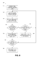
- FIG. 8 is a flowchart illustrating a method for verifying that the optimum notch filter frequency was selected in accordance with various aspects of the present disclosure
- FIG. 9 is a flowchart illustrating a method for detecting shock sensor resonance in a DSD and tuning a notch filter in accordance with various aspects of the present disclosure
- FIG. 10 is a flowchart illustrating a method for verifying that the optimum notch filter frequency was selected in accordance with various aspects of the present disclosure
- FIG. 11 is a flowchart illustrating a method for detecting shock sensor resonance in a DSD and tuning a notch filter in accordance with various aspects of the present disclosure.
- FIG. 12 is a flowchart illustrating a method for verifying that the optimum notch filter frequency was selected in accordance with various aspects of the present disclosure.
- Various aspects of the present disclosure provide methods for detecting the actual resonance frequency for a shock sensor in a DSD.
- the methods may enable a higher Q-factor of the notch filter and hence less propagation delay.
- control unit 150 may control the output frequency of the PWM 140 generating a spindle drive signal 142 .
- the PWM output frequency, and hence the spindle drive signal 142 may be swept within a range of possible shock sensor resonance frequencies, for example, about 44 ⁇ 10 kHz, in order to cause a small vibration signal.
- the noise level of the output signal 162 of the shock detection system 160 may be monitored and may reach a maximum when the output frequency of the PWM 140 (and hence spindle vibration) overlaps with and excites the resonance frequency of the shock sensor 165 . Based on the detected resonance frequency of the shock sensor 165 , a suitable frequency setting may be selected for the notch filter 175 .
- control unit 150 may sample the output signal 162 of the shock detection system 160 and calculate maximum noise, for example as root-mean-square (RMS) noise while controlling the PWM 140 to step through the frequency settings.
- control unit 150 may calculate maximum peak-to-peak (P-P) noise while controlling the output frequency settings of the PWM 140 .
- the notch filter frequency may be selected based on the frequency at which the RMS or P-P noise of the output signal 162 of the shock detection system 160 reaches a maximum.
- FIG. 5 is a graph 500 illustrating example measurements of shock noise versus output frequency of the PWM 140 generating the spindle drive signal 142 for a DSD 100 in accordance with various aspects of the present disclosure.
- P-P noise 530 and RMS noise 540 are plotted with respect to spindle frequency.
- the RMS shock noise varies substantially when the output frequency of the PWM 140 generating the spindle drive signal 142 is adjusted around the frequency at which the peak output signal 162 RMS shock noise is obtained. Shock sensor resonance frequency detection to within ⁇ 1 kHz may be achieved exceeding the current ⁇ 2 kHz requirement.
- multiple voltage settings for window comparators 190 of the shock detection system 160 may be utilized to detect the P-P noise value while adjusting the output frequency settings of the PWM 140 .
- the notch filter frequency may be selected within a predetermined range, for example within ⁇ 2 kHz or another range, of the resonance frequency of the shock sensor 165 .
- the worst-case PWM output frequency (i.e., the output frequency of the PWM 140 generating the spindle drive signal 142 producing the maximum noise level for the output signal 162 of the shock detection system 160 ) may be maintained while adjusting the output frequency settings of the PWM 140 to the nearest available frequency settings to the selected frequency for the notch filter 175 , for example, within a range of about ⁇ 10 kHz or another range, of the selected notch filter frequency.
- the notch filter frequency may be selected within a predetermined range, for example within ⁇ 2 kHz or another range, of the resonance frequency of the shock sensor 165 .
- the notch filter frequency adjustment may eliminate the effect of variations of the actual notch frequency, as compared to the specified value, due to circuit tolerances. If an available frequency setting for the notch filter 175 within the predetermined PWM output frequency range provides increased noise suppression of the output signal 162 of the shock detection system 160 , the available frequency setting for the notch filter 175 may be selected and applied as a new notch filter frequency.
- firmware-tunable filters 180 in the shock detection system 160 are set in a manner that ensures maximum amplification of signals near the resonance frequency of the shock sensor 165 while suppressing other frequencies.
- FIG. 6 is a graph 600 illustrating example gain and phase plots before and after application of a notch filter for a shock detection system output signal 162 in accordance with various aspects of the present disclosure.
- example gain 610 and phase 620 plots of a shock detection system output signal 162
- example gain 630 and phase 640 plots of the shock detection system output signal 162 after a notch filter with a Q-factor of 1.0 when mismatch between the frequency of the notch filter (f notch ) and the resonance frequency of the shock sensor (f sensor ) is reduced in accordance with various aspects of the present disclosure are shown.
- FIG. 7 is a flowchart illustrating a method 700 for detecting shock sensor resonance in a DSD 100 and tuning a notch filter in accordance with various aspects of the present disclosure.
- tunable filters e.g., the firmware-tunable filters 180
- the output frequency of the PWM 140 generating the spindle drive signal 142 may be adjusted up or down in increments of about 200 Hz, or any other increment, within a range of possible shock sensor resonance frequencies, for example about 44 ⁇ 10 kHz or another range, in order to cause a small vibration signal.
- the control unit 150 may control the PWM 140 to repeatedly adjust the output frequency generating the spindle drive signal 142 to the spindle motor 120 up or down in increments of about 200 Hz or another increment.
- the noise level of the output signal 162 of the shock detection system 160 may be monitored as the output frequency of the PWM 140 is adjusted and the noise level may reach a maximum.
- the control unit 150 may sample the output signal 162 of the shock detection system 160 and calculate maximum root-mean-square (RMS) noise while controlling the PWM 140 to step through the output frequency settings.
- the control unit 150 may calculate maximum peak-to-peak (P-P) noise, or any other noise figure of merit, while controlling the PWM 140 to step through the output frequency settings.
- the control unit 150 may determine that the RMS or P-P noise level of the output signal 162 is decreasing from a higher value.
- the control unit 150 may determine that the previous output signal 162 noise level is the maximum noise level. The previous higher value may be determined as the maximum noise level.
- output signal 162 noise levels may be calculated for each PWM frequency setting in a predetermined range of PWM frequency settings, for example about 44 ⁇ 10 kHz or another range, and the maximum output signal 162 noise level selected from the calculated noise levels.
- the output signal 162 noise level may reach a maximum when the output frequency of the PWM 140 overlaps with and excites the resonance frequency of the shock sensor 165 .
- the output frequency of the PWM 140 may continue to be adjusted.
- a notch filter frequency may be selected based on the PWM frequency at the maximum noise level. For example, the notch filter frequency may be selected based on the frequency at which the RMS or P-P noise reaches a maximum. The notch filter frequency may be selected within a predetermined range, for example within ⁇ 2 kHz or another range, of the resonance frequency of the shock sensor 165 .
- the control unit 150 may apply the notch filter 175 having the selected notch filter frequency.
- the worst-case PWM frequency i.e., the output frequency of the PWM 140 generating the spindle drive signal 142 producing the maximum output signal 162 noise level of the shock detection system 160
- the worst-case PWM frequency may be maintained while adjusting the notch filter through the nearest available frequency settings to the selected frequency for the notch filter 175 , for example, within a range of about ⁇ 10 kHz of the selected notch filter frequency.
- the notch filter frequency may be selected within a predetermined range, for example within ⁇ 2 kHz or another range, of the resonance frequency of the shock sensor 165 .
- FIG. 8 is a flowchart illustrating a method 800 for verifying that the optimum notch filter frequency was selected in accordance with various aspects of the present disclosure.
- the control unit 150 may control the PWM 140 to maintain the frequency setting causing the maximum noise level of the shock detection system output signal 162 .
- the notch filter frequency may be adjusted up or down in increments of about 100 Hz or another increment within a range of available notch filter frequency settings around the selected notch filter frequency.
- the control unit 150 may control the notch filter 175 to repeatedly adjust the notch filter frequency setting up or down in increments of about 100 Hz or another increment.
- the noise level of the output signal 162 of the shock detection system 160 may be monitored as the notch filter frequency setting is adjusted.
- the control unit 150 may determine that the noise level of the output signal 162 is decreasing from a higher value.
- the control unit 150 may determine that the current notch filter frequency is a candidate for a new notch filter frequency.
- output signal 162 noise levels may be calculated for each notch filter frequency in a predetermined range of notch filter frequencies around the selected notch filter frequency, for example about 44 ⁇ 10 kHz or another range, and the minimum noise level may be determined.
- the control unit 150 may determine whether the last available frequency setting for the notch filter 175 has been tested. In response to determining that the last available frequency setting for the notch filter 175 has been tested ( 850 —Y), at block 860 the control unit 150 may apply the notch filter 175 having the selected notch filter frequency.
- the method may continue at operation 820 with the next available frequency setting for the notch filter 175 .
- the control unit 150 may select the current notch filter frequency as a new notch filter frequency.
- control unit 150 may determine whether the last available frequency setting for the notch filter 175 has been tested. In response to determining that the last available frequency setting for the notch filter 175 has been tested ( 880 —Y), at block 890 , the control unit 150 may apply the notch filter 175 having the new notch filter frequency.
- the method may continue at operation 820 with the next available frequency setting for the notch filter 175 .
- FIG. 2B is a block diagram illustrating a capacitor drive circuit 210 and an MLCC 220 in accordance with certain aspects of the present disclosure.
- a dedicated MLCC 220 may be positioned near the shock sensor 165 on the printed circuit board (PCB) and may be driven with a capacitor drive circuit 210 incorporated into the DSD 100 , for example as part of the circuitry of a large scale integrated (LSI) circuit (not shown).
- the capacitor drive circuit 210 may be configured to generate an alternating current (AC) voltage signal 212 , for example, but not limited to, a sine wave, a square wave, or a triangle wave, of known frequency near the resonance frequency of the shock sensor 165 to drive the MLCC 220 .
- AC alternating current
- the frequency of the AC voltage signal 212 may be adjusted up or down in increments of about 200 Hz or another increment within a range of possible shock sensor resonance frequencies, for example about 44 ⁇ 10 kHz or another range, in order to cause a small vibration of the MLCC 220 .
- the noise level for the output signal 162 of the shock detection system 160 may reach a maximum value when the MLCC 220 is driven at the resonance frequency of the shock sensor 165 .
- a resonance frequency detection and notch filter selection scheme similar to the scheme described with respect to the spindle drive signal 142 generated by the PWM 140 may be implemented.
- FIG. 9 is a flowchart illustrating a method 900 for detecting shock sensor resonance in a DSD 100 and tuning a notch filter in accordance with various aspects of the present disclosure.
- tunable filters e.g., the firmware-tunable filters 180
- the shock detection system 160 may be set to provide maximum amplification of signal frequencies near a resonance frequency of the shock sensor 165 while suppressing other frequencies.
- the frequency of the AC voltage signal generated by the capacitor drive circuit 210 to drive the MLCC 220 may be adjusted up or down in increments of about 200 Hz or another increment within a range of possible shock sensor resonance frequencies, for example about 44 ⁇ 10 kHz or another range, in order to cause a small vibration in the MLCC 220 .
- the control unit 150 may control the capacitor drive circuit 210 to repeatedly adjust the frequency of the AC voltage signal 212 up or down in increments of about 200 Hz or another increment.
- the noise level of the output signal 162 of the shock detection system 160 may be monitored as the frequency of the AC voltage signal 212 is adjusted and the noise level of the output signal 162 may reach a maximum.
- the control unit 150 may sample the output signal 162 of the shock detection system 160 and calculate maximum root-mean-square (RMS) noise while controlling the capacitor drive circuit 210 to adjust the frequency of the AC voltage signal 212 driving the MLCC 220 .
- the control unit 150 may calculate maximum peak-to-peak (P-P) noise, or any other noise figure of merit, while controlling the capacitor drive circuit 210 to adjust the frequency of the AC voltage signal 212 through the range of frequency settings.
- the control unit 150 may determine that the RMS or P-P noise level of the output signal 162 is decreasing from a higher value.
- the control unit 150 may determine that the previous output signal 162 noise level is the maximum noise level. The previous higher value may be determined as the maximum noise level.
- output signal 162 noise levels may be calculated for each AC voltage signal 212 frequency setting in a predetermined range of frequency settings, for example about 44 ⁇ 10 kHz or another range, and the maximum output signal 162 noise level selected from the calculated noise levels.
- the output signal 162 noise level may reach a maximum when the frequency of the AC voltage signal 212 driving the MLCC 220 overlaps with and excites the resonance frequency of the shock sensor 165 .
- the frequency of the AC voltage signal 212 driving the MLCC 220 may continue to be adjusted.
- a notch filter frequency may be selected based on the frequency of the AC voltage signal 212 at the maximum noise level. For example, the notch filter frequency may be selected based on the frequency at which the RMS or P-P noise reaches a maximum. The notch filter frequency may be selected within a predetermined range, for example within ⁇ 2 kHz or another range, of the resonance frequency of the shock sensor 165 .
- the control unit 150 may apply the notch filter 175 having the selected notch filter frequency.
- the worst-case frequency of the AC voltage signal 212 driving the MLCC 220 i.e., the output of the capacitor drive circuit 210 generating the AC voltage signal 212 producing the maximum output signal 162 noise level of the shock detection system 160
- the worst-case frequency of the AC voltage signal 212 driving the MLCC 220 may be maintained while adjusting the notch filter through the nearest available frequency settings to the selected frequency for the notch filter 175 , for example, within a range of about ⁇ 10 kHz of the selected notch filter frequency.
- the notch filter frequency may be selected within a predetermined range, for example within ⁇ 2 kHz or another range, of the resonance frequency of the shock sensor 165 .
- FIG. 10 is a flowchart illustrating a method 1000 for verifying that the optimum notch filter frequency was selected in accordance with various aspects of the present disclosure.
- the control unit 150 may control the capacitor drive circuit 210 to maintain the frequency setting of the AC voltage signal 212 causing the maximum noise level of the shock detection system output signal 162 .
- the notch filter frequency may be adjusted up or down in increments of about 100 Hz or another increment within a range of available notch filter frequency settings around the selected notch filter frequency.
- the control unit 150 may control the notch filter 175 to repeatedly adjust the notch filter frequency setting up or down in increments of about 100 Hz or another increment.
- the noise level of the output signal 162 of the shock detection system 160 may be monitored as the notch filter frequency setting is adjusted.
- the control unit 150 may determine that the noise level of the output signal 162 is decreasing from a higher value.
- the control unit 150 may determine that the current notch filter frequency is a candidate for a new notch filter frequency
- output signal 162 noise levels may be calculated for each notch filter frequency in a predetermined range of notch filter frequencies around the selected notch filter frequency, for example about 44 ⁇ 10 kHz or another range, and the minimum noise level may be determined.
- the control unit 150 may determine whether the last available frequency setting for the notch filter 175 has been tested. In response to determining that the last available frequency setting for the notch filter 175 has been tested ( 1050 —Y), at block 1060 the control unit 150 may apply the notch filter 175 having the selected notch filter frequency.
- the method may continue at operation 1020 with the next available frequency setting for the notch filter 175 .
- control unit 150 may select the current notch filter frequency as a new notch filter frequency.
- control unit 150 may determine whether the last available frequency setting for the notch filter 175 has been tested. In response to determining that the last available frequency setting for the notch filter 175 has been tested ( 1080 —Y), at block 1090 , the control unit 150 may apply the notch filter 175 having the new notch filter frequency.
- the method may continue at operation 1020 with the next available frequency setting for the notch filter 175 .
- the VCM 135 may be utilized to induce a vibration signal within a range of possible resonance frequencies, for example about 44 ⁇ 10 kHz or another range, of the resonance frequency of the shock sensor 165 .
- the VCM 135 may be driven by a VCM drive signal 157 generated by a VCM control circuit 155 .
- the VCM control circuit 155 may include a current control loop (CCL) and the VCM drive signal 157 may be generated by the CCL.
- CCL current control loop
- the frequency of the VCM drive signal 157 may be adjusted around the resonance frequency of the shock sensor 165 while monitoring the output signal 162 of the shock detection system 160 for a maximum noise level (e.g., maximum RMS noise level or maximum P-P noise level).
- a maximum noise level e.g., maximum RMS noise level or maximum P-P noise level.
- the VCM drive signal 157 may be implemented in firmware and may be, for example, but not limited to, a sine wave, a triangle wave, or a square wave.
- a VCM drive signal 157 having a frequency near or below half of the resonant frequency of the shock sensor 165 may produce harmonics that could excite the resonance causing erroneous results.
- VCM voltage mode excitation of the VCM 135 may be used and the frequency of the VCM voltage drive signal adjusted in small frequency adjustment bands around the resonance frequency of the shock sensor 165 , but for large frequency adjustment bands around the resonance frequency of the shock sensor 165 the VCM voltage drive signal amplitude vs. frequency may be controlled.
- FIG. 11 is a flowchart illustrating a method 1100 for detecting shock sensor resonance in a DSD 100 and tuning a notch filter in accordance with various aspects of the present disclosure.
- tunable filters e.g., the firmware-tunable filters 180
- the shock detection system 160 may be set to provide maximum amplification of signal frequencies near a resonance frequency of the shock sensor 165 while suppressing other frequencies.
- the frequency of the VCM drive signal 157 may be adjusted up or down in increments of about 200 Hz or another increment within a range of possible shock sensor resonance frequencies, for example about 44 ⁇ 10 kHz or another range, in order to cause a small vibration in the VCM 135 .
- the control unit 150 may control the VCM control circuit 155 to repeatedly adjust the frequency of the VCM drive signal 157 up or down in increments of about 200 Hz or another increment.
- the noise level of the output signal 162 of the shock detection system 160 may be monitored as the frequency of the VCM drive signal 157 is adjusted and the noise level of the output signal 162 may reach a maximum.
- the control unit 150 may sample the output signal 162 of the shock detection system 160 and calculate maximum root-mean-square (RMS) noise while controlling the VCM control circuit 155 to adjust the frequency of the VCM drive signal 157 .
- the control unit 150 may calculate maximum peak-to-peak (P-P) noise, or any other noise figure of merit, while controlling the VCM control circuit 155 to adjust the frequency of the VCM drive signal 157 through the range of frequency settings.
- the control unit 150 may determine that the RMS or P-P noise level of the output signal 162 is decreasing from a higher value.
- the control unit 150 may determine that the previous output signal 162 noise level is the maximum noise level. The previous higher value may be determined as the maximum noise level.
- output signal 162 noise levels may be calculated for each VCM drive signal 157 frequency setting in a predetermined range of frequency settings, for example about 44 ⁇ 10 kHz or another range, and the maximum output signal 162 noise level selected from the calculated noise levels.
- the output signal 162 noise level may reach a maximum when the frequency of the VCM drive signal 157 overlaps with and excites the resonance frequency of the shock sensor 165 .
- the frequency of the VCM drive signal 157 may continue to be adjusted.
- a notch filter frequency may be selected based on the frequency of the VCM drive signal 157 at the maximum noise level. For example, the notch filter frequency may be selected based on the frequency at which the RMS or P-P noise reaches a maximum. The notch filter frequency may be selected within a predetermined range, for example within ⁇ 2 kHz or another range, of the resonance frequency of the shock sensor 165 .
- the control unit 150 may apply the notch filter 175 having the selected notch filter frequency
- the worst-case frequency of the VCM drive signal 157 (i.e., the output of the VCM control circuit 155 generating the VCM drive signal 157 producing the maximum output signal 162 noise level of the shock detection system 160 ) may be maintained while adjusting the notch filter through the nearest available frequency settings to the selected frequency for the notch filter 175 , for example, within a range of about ⁇ 10 kHz of the selected notch filter frequency.
- the notch filter frequency may be selected within a predetermined range, for example within ⁇ 2 kHz or another range, of the resonance frequency of the shock sensor 165 .
- FIG. 12 is a flowchart illustrating a method 1200 for verifying that the optimum notch filter frequency was selected in accordance with various aspects of the present disclosure.
- the control unit 150 may control the VCM control circuit 155 to maintain the frequency setting of the VCM drive signal 157 causing the maximum noise level of the shock detection system output signal 162 .
- the notch filter frequency may be adjusted up or down in increments of about 100 Hz or another increment within a range of available notch filter frequency settings around the selected notch filter frequency.
- the control unit 150 may control the notch filter 175 to repeatedly adjust the notch filter frequency setting up or down in increments of about 100 Hz or another increment.
- the noise level of the output signal 162 of the shock detection system 160 may be monitored as the notch filter frequency setting is adjusted.
- the control unit 150 may determine that the noise level of the output signal 162 is decreasing from a higher value.
- the control unit 150 may determine that the current notch filter frequency is a candidate for a new notch filter frequency
- output signal 162 noise levels may be calculated for each notch filter frequency in a predetermined range of notch filter frequencies around the selected notch filter frequency, for example about 44 ⁇ 10 kHz or another range, and the minimum noise level may be determined.
- the control unit 150 may determine whether the last available frequency setting for the notch filter 175 has been tested. In response to determining that the last available frequency setting for the notch filter 175 has been tested ( 1250 —Y), at block 1260 the control unit 150 may apply the notch filter 175 having the selected notch filter frequency.
- the method may continue at operation 1020 with the next available frequency setting for the notch filter 175 .
- the control unit 150 may select the current notch filter frequency as a new notch filter frequency.
- control unit 150 may determine whether the last available frequency setting for the notch filter 175 has been tested. In response to determining that the last available frequency setting for the notch filter 175 has been tested ( 1280 —Y), at block 1290 , the control unit 150 may apply the notch filter 175 having the new notch filter frequency.
- the method may continue at operation 1220 with the next available frequency setting for the notch filter 175 .
- the methods 700 , 900 , and 1100 for detecting shock sensor resonance in a DSD 100 and the method 800 , 1000 , and 1200 for verifying that the optimum notch filter. frequency was selected may be performed as part of factory calibration of the DSD 100 or may be performed as part of DSD 100 calibration in the field
Landscapes
- Physics & Mathematics (AREA)
- General Physics & Mathematics (AREA)
- Spectroscopy & Molecular Physics (AREA)
- Engineering & Computer Science (AREA)
- Computer Networks & Wireless Communication (AREA)
- Signal Processing (AREA)
- Transmission And Conversion Of Sensor Element Output (AREA)
- Measurement Of Mechanical Vibrations Or Ultrasonic Waves (AREA)
Abstract
Description
Claims (30)
Priority Applications (1)
| Application Number | Priority Date | Filing Date | Title |
|---|---|---|---|
| US15/354,867 US9832050B1 (en) | 2016-07-15 | 2016-11-17 | Shock sensor resonance detection for notch filter tuning |
Applications Claiming Priority (2)
| Application Number | Priority Date | Filing Date | Title |
|---|---|---|---|
| US201662362853P | 2016-07-15 | 2016-07-15 | |
| US15/354,867 US9832050B1 (en) | 2016-07-15 | 2016-11-17 | Shock sensor resonance detection for notch filter tuning |
Publications (1)
| Publication Number | Publication Date |
|---|---|
| US9832050B1 true US9832050B1 (en) | 2017-11-28 |
Family
ID=60408662
Family Applications (1)
| Application Number | Title | Priority Date | Filing Date |
|---|---|---|---|
| US15/354,867 Active US9832050B1 (en) | 2016-07-15 | 2016-11-17 | Shock sensor resonance detection for notch filter tuning |
Country Status (1)
| Country | Link |
|---|---|
| US (1) | US9832050B1 (en) |
Cited By (1)
| Publication number | Priority date | Publication date | Assignee | Title |
|---|---|---|---|---|
| CN110266241A (en) * | 2019-06-20 | 2019-09-20 | 哈尔滨工业大学 | Method and device for resonance suppression of servo drive system, and servo drive system |
Citations (4)
| Publication number | Priority date | Publication date | Assignee | Title |
|---|---|---|---|---|
| US20110085260A1 (en) | 2008-12-16 | 2011-04-14 | Toshiaki Wada | Disk drive and servo control method for the disk drive that is responsive to vibration |
| US20110303011A1 (en) | 2010-06-15 | 2011-12-15 | Kai-Mei Camilla Fu | Sensor apparatus, system and method providing coupling characterization |
| US8184389B2 (en) | 2006-04-14 | 2012-05-22 | Seagate Technology Llc | Sensor resonant frequency identification and filter tuning |
| US9099101B1 (en) * | 2014-05-13 | 2015-08-04 | HGST Netherlands B.V. | Acoustic noise control for hard disk drive |
-
2016
- 2016-11-17 US US15/354,867 patent/US9832050B1/en active Active
Patent Citations (4)
| Publication number | Priority date | Publication date | Assignee | Title |
|---|---|---|---|---|
| US8184389B2 (en) | 2006-04-14 | 2012-05-22 | Seagate Technology Llc | Sensor resonant frequency identification and filter tuning |
| US20110085260A1 (en) | 2008-12-16 | 2011-04-14 | Toshiaki Wada | Disk drive and servo control method for the disk drive that is responsive to vibration |
| US20110303011A1 (en) | 2010-06-15 | 2011-12-15 | Kai-Mei Camilla Fu | Sensor apparatus, system and method providing coupling characterization |
| US9099101B1 (en) * | 2014-05-13 | 2015-08-04 | HGST Netherlands B.V. | Acoustic noise control for hard disk drive |
Cited By (2)
| Publication number | Priority date | Publication date | Assignee | Title |
|---|---|---|---|---|
| CN110266241A (en) * | 2019-06-20 | 2019-09-20 | 哈尔滨工业大学 | Method and device for resonance suppression of servo drive system, and servo drive system |
| CN110266241B (en) * | 2019-06-20 | 2021-02-19 | 哈尔滨工业大学 | Method and device for resonance suppression of servo drive system and servo drive system |
Similar Documents
| Publication | Publication Date | Title |
|---|---|---|
| US8179626B1 (en) | Adaptive shock detection | |
| US8314531B2 (en) | Piezoelectric actuator driver circuit | |
| US8508104B2 (en) | Piezoelectric actuator driver circuit | |
| US7199960B1 (en) | Disk drive with AC exciter for head/disk interface | |
| KR100518553B1 (en) | Apparatus and method for suppressing mechanical resonance using an adaptive notch filter | |
| US20190078643A1 (en) | User-tuned, active vibration-isolation system | |
| JP2008016173A (en) | Adaptive system resonance compensation method, recording medium, resonance compensation device, and disk drive | |
| US8804265B2 (en) | Calibration of a resonance frequency filter | |
| US9013825B1 (en) | Electronic system with vibration management mechanism and method of operation thereof | |
| US7602572B2 (en) | Stability margins and error recovery in servo control systems | |
| US20110085260A1 (en) | Disk drive and servo control method for the disk drive that is responsive to vibration | |
| US9832050B1 (en) | Shock sensor resonance detection for notch filter tuning | |
| WO2000016043A1 (en) | Angle speed sensor | |
| US8976483B1 (en) | Rotational vibration compensation using microactuator | |
| US10566014B2 (en) | Data storage device detecting resistance delta of a spin torque oscillator | |
| US12255595B2 (en) | Calibration method, corresponding circuit and apparatus | |
| JP2016194467A (en) | Method for inspecting physical quantity sensor and method for manufacturing physical quantity sensor | |
| CN115097365A (en) | Frequency-variable modulation field system, control method thereof and EPR spectrometer | |
| JPH01321876A (en) | Ultrasonic motor drive device | |
| US7830765B2 (en) | Methods and apparatus to monitor and control hard-disk head position | |
| SE514499C2 (en) | Method and apparatus for compensating electrical interference | |
| JP2007213653A (en) | Interval control device | |
| JP6380850B2 (en) | Toner amount detection device, image forming apparatus, and toner amount detection device adjustment method | |
| WO2025139836A1 (en) | Method for driving a linear resonant actuator | |
| JP2010108560A (en) | Signal amplification device and storage device |
Legal Events
| Date | Code | Title | Description |
|---|---|---|---|
| AS | Assignment |
Owner name: WESTERN DIGITAL TECHNOLOGIES, INC., CALIFORNIA Free format text: ASSIGNMENT OF ASSIGNORS INTEREST;ASSIGNORS:EKLUND, ERIK J.;FERRIS, TIMOTHY A.;SIGNING DATES FROM 20161111 TO 20161114;REEL/FRAME:040364/0228 |
|
| STCF | Information on status: patent grant |
Free format text: PATENTED CASE |
|
| AS | Assignment |
Owner name: JPMORGAN CHASE BANK, N.A., AS AGENT, ILLINOIS Free format text: SECURITY INTEREST;ASSIGNOR:WESTERN DIGITAL TECHNOLOGIES, INC.;REEL/FRAME:052915/0566 Effective date: 20200113 |
|
| MAFP | Maintenance fee payment |
Free format text: PAYMENT OF MAINTENANCE FEE, 4TH YEAR, LARGE ENTITY (ORIGINAL EVENT CODE: M1551); ENTITY STATUS OF PATENT OWNER: LARGE ENTITY Year of fee payment: 4 |
|
| AS | Assignment |
Owner name: WESTERN DIGITAL TECHNOLOGIES, INC., CALIFORNIA Free format text: RELEASE OF SECURITY INTEREST AT REEL 052915 FRAME 0566;ASSIGNOR:JPMORGAN CHASE BANK, N.A.;REEL/FRAME:059127/0001 Effective date: 20220203 |
|
| AS | Assignment |
Owner name: JPMORGAN CHASE BANK, N.A., ILLINOIS Free format text: PATENT COLLATERAL AGREEMENT - A&R LOAN AGREEMENT;ASSIGNOR:WESTERN DIGITAL TECHNOLOGIES, INC.;REEL/FRAME:064715/0001 Effective date: 20230818 Owner name: JPMORGAN CHASE BANK, N.A., ILLINOIS Free format text: PATENT COLLATERAL AGREEMENT - DDTL LOAN AGREEMENT;ASSIGNOR:WESTERN DIGITAL TECHNOLOGIES, INC.;REEL/FRAME:067045/0156 Effective date: 20230818 |
|
| MAFP | Maintenance fee payment |
Free format text: PAYMENT OF MAINTENANCE FEE, 8TH YEAR, LARGE ENTITY (ORIGINAL EVENT CODE: M1552); ENTITY STATUS OF PATENT OWNER: LARGE ENTITY Year of fee payment: 8 |