US9831792B1 - Buck-boost power conversion circuit - Google Patents
Buck-boost power conversion circuit Download PDFInfo
- Publication number
- US9831792B1 US9831792B1 US15/350,469 US201615350469A US9831792B1 US 9831792 B1 US9831792 B1 US 9831792B1 US 201615350469 A US201615350469 A US 201615350469A US 9831792 B1 US9831792 B1 US 9831792B1
- Authority
- US
- United States
- Prior art keywords
- active switch
- buck
- power conversion
- conversion circuit
- inductor
- Prior art date
- Legal status (The legal status is an assumption and is not a legal conclusion. Google has not performed a legal analysis and makes no representation as to the accuracy of the status listed.)
- Expired - Fee Related
Links
Images


Classifications
-
- H—ELECTRICITY
- H02—GENERATION; CONVERSION OR DISTRIBUTION OF ELECTRIC POWER
- H02M—APPARATUS FOR CONVERSION BETWEEN AC AND AC, BETWEEN AC AND DC, OR BETWEEN DC AND DC, AND FOR USE WITH MAINS OR SIMILAR POWER SUPPLY SYSTEMS; CONVERSION OF DC OR AC INPUT POWER INTO SURGE OUTPUT POWER; CONTROL OR REGULATION THEREOF
- H02M3/00—Conversion of DC power input into DC power output
- H02M3/22—Conversion of DC power input into DC power output with intermediate conversion into AC
- H02M3/24—Conversion of DC power input into DC power output with intermediate conversion into AC by static converters
- H02M3/28—Conversion of DC power input into DC power output with intermediate conversion into AC by static converters using discharge tubes with control electrode or semiconductor devices with control electrode to produce the intermediate AC
- H02M3/325—Conversion of DC power input into DC power output with intermediate conversion into AC by static converters using discharge tubes with control electrode or semiconductor devices with control electrode to produce the intermediate AC using devices of a triode or a transistor type requiring continuous application of a control signal
- H02M3/335—Conversion of DC power input into DC power output with intermediate conversion into AC by static converters using discharge tubes with control electrode or semiconductor devices with control electrode to produce the intermediate AC using devices of a triode or a transistor type requiring continuous application of a control signal using semiconductor devices only
- H02M3/337—Conversion of DC power input into DC power output with intermediate conversion into AC by static converters using discharge tubes with control electrode or semiconductor devices with control electrode to produce the intermediate AC using devices of a triode or a transistor type requiring continuous application of a control signal using semiconductor devices only in push-pull configuration
- H02M3/3376—Conversion of DC power input into DC power output with intermediate conversion into AC by static converters using discharge tubes with control electrode or semiconductor devices with control electrode to produce the intermediate AC using devices of a triode or a transistor type requiring continuous application of a control signal using semiconductor devices only in push-pull configuration with automatic control of output voltage or current
- H02M3/3378—Conversion of DC power input into DC power output with intermediate conversion into AC by static converters using discharge tubes with control electrode or semiconductor devices with control electrode to produce the intermediate AC using devices of a triode or a transistor type requiring continuous application of a control signal using semiconductor devices only in push-pull configuration with automatic control of output voltage or current in a push-pull configuration of the parallel type
-
- H—ELECTRICITY
- H02—GENERATION; CONVERSION OR DISTRIBUTION OF ELECTRIC POWER
- H02M—APPARATUS FOR CONVERSION BETWEEN AC AND AC, BETWEEN AC AND DC, OR BETWEEN DC AND DC, AND FOR USE WITH MAINS OR SIMILAR POWER SUPPLY SYSTEMS; CONVERSION OF DC OR AC INPUT POWER INTO SURGE OUTPUT POWER; CONTROL OR REGULATION THEREOF
- H02M3/00—Conversion of DC power input into DC power output
- H02M3/02—Conversion of DC power input into DC power output without intermediate conversion into AC
- H02M3/04—Conversion of DC power input into DC power output without intermediate conversion into AC by static converters
- H02M3/10—Conversion of DC power input into DC power output without intermediate conversion into AC by static converters using discharge tubes with control electrode or semiconductor devices with control electrode
- H02M3/145—Conversion of DC power input into DC power output without intermediate conversion into AC by static converters using discharge tubes with control electrode or semiconductor devices with control electrode using devices of a triode or transistor type requiring continuous application of a control signal
- H02M3/155—Conversion of DC power input into DC power output without intermediate conversion into AC by static converters using discharge tubes with control electrode or semiconductor devices with control electrode using devices of a triode or transistor type requiring continuous application of a control signal using semiconductor devices only
- H02M3/156—Conversion of DC power input into DC power output without intermediate conversion into AC by static converters using discharge tubes with control electrode or semiconductor devices with control electrode using devices of a triode or transistor type requiring continuous application of a control signal using semiconductor devices only with automatic control of output voltage or current, e.g. switching regulators
- H02M3/158—Conversion of DC power input into DC power output without intermediate conversion into AC by static converters using discharge tubes with control electrode or semiconductor devices with control electrode using devices of a triode or transistor type requiring continuous application of a control signal using semiconductor devices only with automatic control of output voltage or current, e.g. switching regulators including plural semiconductor devices as final control devices for a single load
- H02M3/1582—Buck-boost converters
-
- H—ELECTRICITY
- H02—GENERATION; CONVERSION OR DISTRIBUTION OF ELECTRIC POWER
- H02M—APPARATUS FOR CONVERSION BETWEEN AC AND AC, BETWEEN AC AND DC, OR BETWEEN DC AND DC, AND FOR USE WITH MAINS OR SIMILAR POWER SUPPLY SYSTEMS; CONVERSION OF DC OR AC INPUT POWER INTO SURGE OUTPUT POWER; CONTROL OR REGULATION THEREOF
- H02M1/00—Details of apparatus for conversion
- H02M1/08—Circuits specially adapted for the generation of control voltages for semiconductor devices incorporated in static converters
- H02M1/088—Circuits specially adapted for the generation of control voltages for semiconductor devices incorporated in static converters for the simultaneous control of series or parallel connected semiconductor devices
-
- H—ELECTRICITY
- H02—GENERATION; CONVERSION OR DISTRIBUTION OF ELECTRIC POWER
- H02M—APPARATUS FOR CONVERSION BETWEEN AC AND AC, BETWEEN AC AND DC, OR BETWEEN DC AND DC, AND FOR USE WITH MAINS OR SIMILAR POWER SUPPLY SYSTEMS; CONVERSION OF DC OR AC INPUT POWER INTO SURGE OUTPUT POWER; CONTROL OR REGULATION THEREOF
- H02M1/00—Details of apparatus for conversion
- H02M1/0003—Details of control, feedback or regulation circuits
- H02M1/0009—Devices or circuits for detecting current in a converter
-
- H02M2001/0009—
Definitions
- the present invention relates to a buck-boost power conversion circuit, particularly to a buck-boost power conversion circuit with a center-tapped current transformation element.
- the current industry uses a Hall element 302 to undertake measurement, wherein the Hall element 302 is cascaded to the inductor 301 to acquire the inductor current.
- the Hall element 302 is usually bulky, occupying more layout space and unfavorable to miniaturization of the electronic devices.
- the Hall element 302 is more expensive and will raise the overall cost of the circuit.
- a US patent No. 2016/0036326 disclosed a power supply control circuit, which comprises an emulator circuit.
- the emulator circuit includes a first input terminal and a second input terminal.
- the first input terminal receives a first input value.
- the first input value indicates the magnitude of an input voltage used by a power supply circuit, whereby to generate an output voltage for loads.
- the second input terminal receives a second input value.
- the second input value indicates the magnitude of an output voltage generated by the power supply circuit.
- the emulator circuit uses the input voltage and the output voltage to simulate an inductor current flowing through the power supply circuit. Although the prior art can acquire the value of the inductor current, the circuit thereof is very complicated and unfavorable for application.
- One objective of the present invention is to solve the problems occurring in the conventional technology.
- the present invention provides a buck-boost power conversion circuit, which is connected with a power source and receives the electric power supplied by the power source.
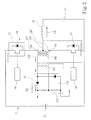
- the buck-boost power conversion circuit comprises a first active switch, a second active switch, an inductor, a center-tapped current transformation element, and a signal rectification unit.
- the first active switch is cascaded to the second active switch to form a branch circuit.
- the branch circuit is connected in parallel with the power source.
- the inductor is connected with a capacitor.
- the center-tapped transformation element includes a primary winding and a secondary winding. Two terminals of the primary winding are respectively connected with the first active switch and the second active switch.
- the primary winding includes a tapped terminal connected with the inductor. While the first active switch or the second active switch is turned on, the primary winding supplies power to the inductor through the tapped terminal. Simultaneously, the secondary winding is induced to generate a magnetic induction signal.
- the signal rectification unit is connected with the secondary winding, receiving the magnetic induction signal and rectifying the magnetic induction signal to generate a current sensation signal corresponding to the current of the inductor.
- the center-tapped current transformation element includes a first sub-winding connected with the first active source and the tapped terminal; and a second sub-winding connected with the second active switch and the tapped terminal.
- the signal rectification unit includes a conversion resistor connected with the second winding in parallel and a rectification circuit connected with the conversion resistor in parallel.
- the rectification circuit is a full-wave rectification circuit or a half-wave rectification circuit.
- the signal rectification unit includes a voltage regulation unit connected with the rectification circuit in parallel.
- the buck-boost power conversion circuit further comprises an on-off control unit connected with the first active switch and the second active switch.
- the second active switch is a transistor, a metal-oxide-semiconductor field-effect transistor, or an insulated gate bipolar transistor.
- the present invention has the following characteristics: no matter whether the first active switch or the second active switch is turned on, the present invention can generate the magnetic induction signal through the center-tapped current transformation element; the present invention rectifies the magnetic induction signal to acquire a current sensation signal corresponding to the current of the inductor, whereby the engineers can learn the variation of the current of the inductor through the current sensation signal; the present invention can solve the problems of the conventional elements: bulkiness, high price, and complicated circuit.
- FIG. 1 is a diagram schematically showing a conventional circuit
- FIG. 2 is a diagram schematically showing a buck-boost power conversion circuit according to one embodiment of the present invention
- FIG. 3 is a diagram schematically showing a buck-boost power conversion circuit according to another embodiment of the present invention.
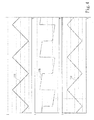
- FIG. 4 is a diagram schematically showing waveforms acquired in a simulation using a continuous conduction mode (CCM) according to one embodiment of the present invention
- FIG. 5 is a diagram schematically showing waveforms acquired in a simulation using a critical conduction mode (CRM) according to one embodiment of the present invention.
- FIG. 6 is a diagram schematically showing waveforms acquired in a simulation using a discontinuous conduction mode (DCM) according to one embodiment of the present invention.
- DCM discontinuous conduction mode
- the present invention provides a buck-boost power conversion circuit 1 , which is connected with a power source 2 , receives the electric power supplied by the power source 2 , and converts the electric power into a working power.
- the power source 2 is a direct-current power source or an alternating-current power source. While the power source 2 is an alternating-current power source, a converter must be disposed between the buck-boost power conversion circuit 1 and the alternating-current power source, converting the alternating-current working power into a direct-current working power source.
- the buck-boost power conversion circuit 1 comprises a first active switch 11 , a second active switch 12 , an inductor 13 , a center-tapped current transformation element 14 , and a signal rectification unit 15 .
- the first active switch 11 is cascaded to the second active switch 12 to form a branch circuit 16 .
- the branch circuit 16 is connected in parallel with the power source 2 .
- the first active switch 11 may be a transistor, a metal-oxide-semiconductor field-effect transistor, or an insulated gate bipolar transistor.
- the second active switch 12 may also be a transistor, a metal-oxide-semiconductor field-effect transistor, or an insulated gate bipolar transistor.
- the first active switch 11 and the second active switch 12 are realized by the same type of switch elements.
- the first active switch 11 is a transistor
- the second active switch 12 is also a transistor.
- the buck-boost power conversion circuit 1 further comprises an on-off control unit 18 connected with the first active switch 11 and the second active switch 12 . After started, the on-off control unit 18 respectively outputs control signals to the first active switch 11 and the second active switch 12 to make the first active switch 11 and the second active switch 12 turn on or off according to the control signals.
- the present invention While intending to boost the power supplied by the power source 2 for feedback, the present invention inverses the pulses of the control signals to make the first active switch 11 turn on later than the second active switch 12 and then the first active switch 11 and the second active switch 12 turn on alternately, whereby the circuit of the present invention can boost the power. While intending to buck the power supplied by the power source 2 , the present invention uses the pulses of the control signals to make the first active switch 11 turn on earlier than the second active switch 12 and then the first active switch 11 and the second active switch 12 turn on alternately, whereby the circuit of the present invention can buck the power.
- the inductor 13 is connected with a capacitor 17 , and the two terminals of the capacitor 17 function as the output terminals of the buck-boost power conversion circuit 1 of the present invention.
- the center-tapped current transformation element 14 includes a primary winding 141 and a secondary winding 142 , wherein the turns ratio of the primary winding 141 and the secondary winding 142 are adjusted according to the requirement of application.
- the two terminals of the primary winding 141 are respectively connected with the first active switch 11 and the second active switch 12 ; the primary winding 141 includes a tapped terminal 143 connected with the inductor 13 .
- the primary winding 141 includes a first sub-winding 144 connected with the first active switch 11 and the tapped terminal 143 ; and a second sub-winding 145 connected with the second active switch 12 and the tapped terminal 143 . While the current is received by the primary winding 141 and flows through the primary winding 141 , the secondary winding 142 is induced magnetically by the primary winding 141 to generate a magnetic induction signal 146 .
- the signal rectification unit 15 is connected with the secondary winding 142 , receiving the magnetic induction signal 146 from the secondary winding 142 and rectifying the magnetic induction signal 146 to generate a current sensation signal 151 , which is corresponding to a current 131 of the inductor 13 and used to indicate the variation of the current 131 of the inductor 13 .
- the signal rectification unit 15 includes a conversion resistor 152 connected in parallel with the secondary winding 142 and a rectification circuit 153 connected in parallel with the conversion resistor 152 .
- the conversion resistor 152 modifies the characteristic of the magnetic induction signal 146 to emphasize the characteristic of the current and favor the working of the rectification circuit 153 .
- the rectification circuit 153 may be a half-wave rectification circuit (as shown in FIG. 2 ) or a full-wave rectification circuit (as shown in FIG. 3 ).
- the signal rectification unit 15 further includes a voltage regulation unit 154 connected in parallel with the rectification circuit 153 .
- the voltage regulation unit 154 is connected with a signal procession unit (not shown in the drawings) in the rear stage thereof.
- the signal procession unit receives the current sensation signal 151 and performs a preset procession on the current sensation signal 151 .
- the voltage regulation unit 154 is a voltage division circuit, undertaking a corresponding impedance matching according to the signal voltage range allowed by the signal procession unit.
- the first active switch 11 and the second active switch 12 are respectively controlled by the on-off control unit 18 to turn on/off. While the first active switch 11 turns on and the second active switch turns off, the current flows through the first sub-winding 144 , and the secondary winding 142 is induced magnetically by the first sub-winding 144 to generate the magnetic induction signal 146 . While the first active switch 11 turns off and the second active switch 12 turns on, the current flows through the second sub-winding 145 , and the secondary winding 142 is induced magnetically to generate the magnetic induction signal 146 .
- the center-tapped current transformation element 14 can always receive the current 131 flowing to the inductor 13 to generate the magnetic induction signal 146 , whereby the magnetic induction signal 146 can fully present the variation of the current 131 of the inductor 13 .
- the circuit disclosed in FIG. 2 is used to simulate the present invention in a continuous conduction mode (CCM), a critical conduction mode (CRM) and a discontinuous conduction mode (DCM).
- CCM continuous conduction mode
- CCM critical conduction mode
- DCM discontinuous conduction mode
- the currents 131 of the inductor 13 , the magnetic induction signals 146 , and the current sensation signals 151 which are obtained in the three modes of simulations, are respectively shown in FIGS. 4-6 . From FIGS. 4-6 , it is learned that the waveform of the current sensation signal 151 is substantially the same as the waveform of the current 131 of the inductor 13 . Therefore, it is proved that the structure of the present invention can indeed be used to detect the current 131 of the inductor 13 .
Landscapes
- Engineering & Computer Science (AREA)
- Power Engineering (AREA)
- Dc-Dc Converters (AREA)
Abstract
Description
Claims (9)
Priority Applications (1)
| Application Number | Priority Date | Filing Date | Title |
|---|---|---|---|
| US15/350,469 US9831792B1 (en) | 2016-11-14 | 2016-11-14 | Buck-boost power conversion circuit |
Applications Claiming Priority (1)
| Application Number | Priority Date | Filing Date | Title |
|---|---|---|---|
| US15/350,469 US9831792B1 (en) | 2016-11-14 | 2016-11-14 | Buck-boost power conversion circuit |
Publications (1)
| Publication Number | Publication Date |
|---|---|
| US9831792B1 true US9831792B1 (en) | 2017-11-28 |
Family
ID=60407749
Family Applications (1)
| Application Number | Title | Priority Date | Filing Date |
|---|---|---|---|
| US15/350,469 Expired - Fee Related US9831792B1 (en) | 2016-11-14 | 2016-11-14 | Buck-boost power conversion circuit |
Country Status (1)
| Country | Link |
|---|---|
| US (1) | US9831792B1 (en) |
Citations (2)
| Publication number | Priority date | Publication date | Assignee | Title |
|---|---|---|---|---|
| US20160036326A1 (en) | 2014-07-29 | 2016-02-04 | International Rectifier Corporation | Power supply control and current emulation |
| US9401653B2 (en) * | 2014-09-04 | 2016-07-26 | Bose Corporation | Power supply with switching converter |
-
2016
- 2016-11-14 US US15/350,469 patent/US9831792B1/en not_active Expired - Fee Related
Patent Citations (2)
| Publication number | Priority date | Publication date | Assignee | Title |
|---|---|---|---|---|
| US20160036326A1 (en) | 2014-07-29 | 2016-02-04 | International Rectifier Corporation | Power supply control and current emulation |
| US9401653B2 (en) * | 2014-09-04 | 2016-07-26 | Bose Corporation | Power supply with switching converter |
Similar Documents
| Publication | Publication Date | Title |
|---|---|---|
| CN108206634B (en) | Insulating synchronous rectification DC/DC converter, controller, adapter and equipment | |
| US8947894B2 (en) | Switched mode power supply including a flyback converter with primary side control | |
| US10291113B2 (en) | Flyback power converter circuit and primary side controller circuit thereof | |
| US9356519B2 (en) | Current balance circuit of resonant type switching power-supply circuit | |
| CN102013800B (en) | Power conversion device | |
| JP7328748B2 (en) | power converter | |
| US11451161B2 (en) | Power switcher, power rectifier, and power converter including cascode-connected transistors | |
| CN107046368B (en) | Power supply conversion device | |
| CN104980030B (en) | Isolated power supply circuit with programmable function and control method thereof | |
| US11165361B2 (en) | Power supply and medical system | |
| US9831792B1 (en) | Buck-boost power conversion circuit | |
| CN106300970A (en) | Step-down converter and step-down conversion device | |
| JP2008289334A (en) | Switching power supply device and power supply control method | |
| CN204189593U (en) | Number of turn adjustable transformer | |
| CN102545621A (en) | Switching power supply and control method thereof | |
| CN107222088A (en) | Control module, switching type power supply device and peak current mode control method | |
| JP2020174465A (en) | Insulated power factor improving device for three-phase AC | |
| US9887632B1 (en) | Step-up KP ripple free converter | |
| US9762123B1 (en) | Boost converter circuit able to sense current | |
| TW201717532A (en) | Single-stage AC-to-DC converter | |
| JP2013062936A (en) | Isolated converter | |
| CN206164369U (en) | Boost-buck power conversion circuit | |
| TWI579570B (en) | Step - down power conversion circuit | |
| US20240421715A1 (en) | Converter and method for bringing an actual transformation ratio into line with a target transformation ratio | |
| US9823675B2 (en) | Tunable DC voltage generating circuit |
Legal Events
| Date | Code | Title | Description |
|---|---|---|---|
| AS | Assignment |
Owner name: SEA SONIC ELECTRONICS CO., LTD., TAIWAN Free format text: ASSIGNMENT OF ASSIGNORS INTEREST;ASSIGNORS:LIN, PAO-TSUN;CHEN, TEN-CHUN;REEL/FRAME:040453/0933 Effective date: 20161024 |
|
| STCF | Information on status: patent grant |
Free format text: PATENTED CASE |
|
| MAFP | Maintenance fee payment |
Free format text: PAYMENT OF MAINTENANCE FEE, 4TH YR, SMALL ENTITY (ORIGINAL EVENT CODE: M2551); ENTITY STATUS OF PATENT OWNER: SMALL ENTITY Year of fee payment: 4 |
|
| FEPP | Fee payment procedure |
Free format text: MAINTENANCE FEE REMINDER MAILED (ORIGINAL EVENT CODE: REM.); ENTITY STATUS OF PATENT OWNER: SMALL ENTITY |
|
| LAPS | Lapse for failure to pay maintenance fees |
Free format text: PATENT EXPIRED FOR FAILURE TO PAY MAINTENANCE FEES (ORIGINAL EVENT CODE: EXP.); ENTITY STATUS OF PATENT OWNER: SMALL ENTITY |
|
| STCH | Information on status: patent discontinuation |
Free format text: PATENT EXPIRED DUE TO NONPAYMENT OF MAINTENANCE FEES UNDER 37 CFR 1.362 |
|
| FP | Lapsed due to failure to pay maintenance fee |
Effective date: 20251128 |