US9831784B2 - Electronic resonant and insulated half-bridge zeta converter - Google Patents
Electronic resonant and insulated half-bridge zeta converter Download PDFInfo
- Publication number
- US9831784B2 US9831784B2 US15/024,360 US201415024360A US9831784B2 US 9831784 B2 US9831784 B2 US 9831784B2 US 201415024360 A US201415024360 A US 201415024360A US 9831784 B2 US9831784 B2 US 9831784B2
- Authority
- US
- United States
- Prior art keywords
- switch
- time interval
- transformer
- inductance
- electronic
- Prior art date
- Legal status (The legal status is an assumption and is not a legal conclusion. Google has not performed a legal analysis and makes no representation as to the accuracy of the status listed.)
- Active
Links
Images


Classifications
-
- H—ELECTRICITY
- H05—ELECTRIC TECHNIQUES NOT OTHERWISE PROVIDED FOR
- H05B—ELECTRIC HEATING; ELECTRIC LIGHT SOURCES NOT OTHERWISE PROVIDED FOR; CIRCUIT ARRANGEMENTS FOR ELECTRIC LIGHT SOURCES, IN GENERAL
- H05B45/00—Circuit arrangements for operating light-emitting diodes [LED]
- H05B45/30—Driver circuits
- H05B45/37—Converter circuits
- H05B45/3725—Switched mode power supply [SMPS]
- H05B45/39—Circuits containing inverter bridges
-
- H—ELECTRICITY
- H02—GENERATION; CONVERSION OR DISTRIBUTION OF ELECTRIC POWER
- H02M—APPARATUS FOR CONVERSION BETWEEN AC AND AC, BETWEEN AC AND DC, OR BETWEEN DC AND DC, AND FOR USE WITH MAINS OR SIMILAR POWER SUPPLY SYSTEMS; CONVERSION OF DC OR AC INPUT POWER INTO SURGE OUTPUT POWER; CONTROL OR REGULATION THEREOF
- H02M3/00—Conversion of DC power input into DC power output
- H02M3/22—Conversion of DC power input into DC power output with intermediate conversion into AC
- H02M3/24—Conversion of DC power input into DC power output with intermediate conversion into AC by static converters
- H02M3/28—Conversion of DC power input into DC power output with intermediate conversion into AC by static converters using discharge tubes with control electrode or semiconductor devices with control electrode to produce the intermediate AC
- H02M3/325—Conversion of DC power input into DC power output with intermediate conversion into AC by static converters using discharge tubes with control electrode or semiconductor devices with control electrode to produce the intermediate AC using devices of a triode or a transistor type requiring continuous application of a control signal
- H02M3/335—Conversion of DC power input into DC power output with intermediate conversion into AC by static converters using discharge tubes with control electrode or semiconductor devices with control electrode to produce the intermediate AC using devices of a triode or a transistor type requiring continuous application of a control signal using semiconductor devices only
- H02M3/33538—Conversion of DC power input into DC power output with intermediate conversion into AC by static converters using discharge tubes with control electrode or semiconductor devices with control electrode to produce the intermediate AC using devices of a triode or a transistor type requiring continuous application of a control signal using semiconductor devices only of the forward type
- H02M3/33546—Conversion of DC power input into DC power output with intermediate conversion into AC by static converters using discharge tubes with control electrode or semiconductor devices with control electrode to produce the intermediate AC using devices of a triode or a transistor type requiring continuous application of a control signal using semiconductor devices only of the forward type with automatic control of the output voltage or current
-
- H—ELECTRICITY
- H02—GENERATION; CONVERSION OR DISTRIBUTION OF ELECTRIC POWER
- H02M—APPARATUS FOR CONVERSION BETWEEN AC AND AC, BETWEEN AC AND DC, OR BETWEEN DC AND DC, AND FOR USE WITH MAINS OR SIMILAR POWER SUPPLY SYSTEMS; CONVERSION OF DC OR AC INPUT POWER INTO SURGE OUTPUT POWER; CONTROL OR REGULATION THEREOF
- H02M1/00—Details of apparatus for conversion
- H02M1/08—Circuits specially adapted for the generation of control voltages for semiconductor devices incorporated in static converters
-
- H—ELECTRICITY
- H02—GENERATION; CONVERSION OR DISTRIBUTION OF ELECTRIC POWER
- H02M—APPARATUS FOR CONVERSION BETWEEN AC AND AC, BETWEEN AC AND DC, OR BETWEEN DC AND DC, AND FOR USE WITH MAINS OR SIMILAR POWER SUPPLY SYSTEMS; CONVERSION OF DC OR AC INPUT POWER INTO SURGE OUTPUT POWER; CONTROL OR REGULATION THEREOF
- H02M1/00—Details of apparatus for conversion
- H02M1/42—Circuits or arrangements for compensating for or adjusting power factor in converters or inverters
- H02M1/4208—Arrangements for improving power factor of AC input
- H02M1/4241—Arrangements for improving power factor of AC input using a resonant converter
-
- H—ELECTRICITY
- H02—GENERATION; CONVERSION OR DISTRIBUTION OF ELECTRIC POWER
- H02M—APPARATUS FOR CONVERSION BETWEEN AC AND AC, BETWEEN AC AND DC, OR BETWEEN DC AND DC, AND FOR USE WITH MAINS OR SIMILAR POWER SUPPLY SYSTEMS; CONVERSION OF DC OR AC INPUT POWER INTO SURGE OUTPUT POWER; CONTROL OR REGULATION THEREOF
- H02M3/00—Conversion of DC power input into DC power output
- H02M3/22—Conversion of DC power input into DC power output with intermediate conversion into AC
- H02M3/24—Conversion of DC power input into DC power output with intermediate conversion into AC by static converters
- H02M3/28—Conversion of DC power input into DC power output with intermediate conversion into AC by static converters using discharge tubes with control electrode or semiconductor devices with control electrode to produce the intermediate AC
- H02M3/325—Conversion of DC power input into DC power output with intermediate conversion into AC by static converters using discharge tubes with control electrode or semiconductor devices with control electrode to produce the intermediate AC using devices of a triode or a transistor type requiring continuous application of a control signal
- H02M3/335—Conversion of DC power input into DC power output with intermediate conversion into AC by static converters using discharge tubes with control electrode or semiconductor devices with control electrode to produce the intermediate AC using devices of a triode or a transistor type requiring continuous application of a control signal using semiconductor devices only
- H02M3/337—Conversion of DC power input into DC power output with intermediate conversion into AC by static converters using discharge tubes with control electrode or semiconductor devices with control electrode to produce the intermediate AC using devices of a triode or a transistor type requiring continuous application of a control signal using semiconductor devices only in push-pull configuration
- H02M3/3376—Conversion of DC power input into DC power output with intermediate conversion into AC by static converters using discharge tubes with control electrode or semiconductor devices with control electrode to produce the intermediate AC using devices of a triode or a transistor type requiring continuous application of a control signal using semiconductor devices only in push-pull configuration with automatic control of output voltage or current
-
- H05B33/0815—
-
- H—ELECTRICITY
- H05—ELECTRIC TECHNIQUES NOT OTHERWISE PROVIDED FOR
- H05B—ELECTRIC HEATING; ELECTRIC LIGHT SOURCES NOT OTHERWISE PROVIDED FOR; CIRCUIT ARRANGEMENTS FOR ELECTRIC LIGHT SOURCES, IN GENERAL
- H05B45/00—Circuit arrangements for operating light-emitting diodes [LED]
- H05B45/30—Driver circuits
- H05B45/37—Converter circuits
- H05B45/3725—Switched mode power supply [SMPS]
- H05B45/382—Switched mode power supply [SMPS] with galvanic isolation between input and output
-
- H—ELECTRICITY
- H02—GENERATION; CONVERSION OR DISTRIBUTION OF ELECTRIC POWER
- H02M—APPARATUS FOR CONVERSION BETWEEN AC AND AC, BETWEEN AC AND DC, OR BETWEEN DC AND DC, AND FOR USE WITH MAINS OR SIMILAR POWER SUPPLY SYSTEMS; CONVERSION OF DC OR AC INPUT POWER INTO SURGE OUTPUT POWER; CONTROL OR REGULATION THEREOF
- H02M1/00—Details of apparatus for conversion
- H02M1/0003—Details of control, feedback or regulation circuits
- H02M1/0009—Devices or circuits for detecting current in a converter
-
- H—ELECTRICITY
- H02—GENERATION; CONVERSION OR DISTRIBUTION OF ELECTRIC POWER
- H02M—APPARATUS FOR CONVERSION BETWEEN AC AND AC, BETWEEN AC AND DC, OR BETWEEN DC AND DC, AND FOR USE WITH MAINS OR SIMILAR POWER SUPPLY SYSTEMS; CONVERSION OF DC OR AC INPUT POWER INTO SURGE OUTPUT POWER; CONTROL OR REGULATION THEREOF
- H02M1/00—Details of apparatus for conversion
- H02M1/0048—Circuits or arrangements for reducing losses
- H02M1/0054—Transistor switching losses
- H02M1/0058—Transistor switching losses by employing soft switching techniques, i.e. commutation of transistors when applied voltage is zero or when current flow is zero
-
- H02M2001/0009—
-
- H02M2001/0058—
-
- Y—GENERAL TAGGING OF NEW TECHNOLOGICAL DEVELOPMENTS; GENERAL TAGGING OF CROSS-SECTIONAL TECHNOLOGIES SPANNING OVER SEVERAL SECTIONS OF THE IPC; TECHNICAL SUBJECTS COVERED BY FORMER USPC CROSS-REFERENCE ART COLLECTIONS [XRACs] AND DIGESTS
- Y02—TECHNOLOGIES OR APPLICATIONS FOR MITIGATION OR ADAPTATION AGAINST CLIMATE CHANGE
- Y02B—CLIMATE CHANGE MITIGATION TECHNOLOGIES RELATED TO BUILDINGS, e.g. HOUSING, HOUSE APPLIANCES OR RELATED END-USER APPLICATIONS
- Y02B20/00—Energy efficient lighting technologies, e.g. halogen lamps or gas discharge lamps
- Y02B20/30—Semiconductor lamps, e.g. solid state lamps [SSL] light emitting diodes [LED] or organic LED [OLED]
-
- Y02B20/346—
-
- Y02B20/348—
-
- Y—GENERAL TAGGING OF NEW TECHNOLOGICAL DEVELOPMENTS; GENERAL TAGGING OF CROSS-SECTIONAL TECHNOLOGIES SPANNING OVER SEVERAL SECTIONS OF THE IPC; TECHNICAL SUBJECTS COVERED BY FORMER USPC CROSS-REFERENCE ART COLLECTIONS [XRACs] AND DIGESTS
- Y02—TECHNOLOGIES OR APPLICATIONS FOR MITIGATION OR ADAPTATION AGAINST CLIMATE CHANGE
- Y02B—CLIMATE CHANGE MITIGATION TECHNOLOGIES RELATED TO BUILDINGS, e.g. HOUSING, HOUSE APPLIANCES OR RELATED END-USER APPLICATIONS
- Y02B70/00—Technologies for an efficient end-user side electric power management and consumption
- Y02B70/10—Technologies improving the efficiency by using switched-mode power supplies [SMPS], i.e. efficient power electronics conversion e.g. power factor correction or reduction of losses in power supplies or efficient standby modes
-
- Y02B70/1433—
-
- Y02B70/1491—
Definitions
- Various embodiments relate to electronic converters.
- Various embodiments provide the driving of a half bridge ZETA converter.
- Electronic converters for light sources including, for example, at least one LED (Light Emitting Diode) or other solid-state lighting devices, may supply a direct current output. Such a current may be steady or else may vary in time, for example, in order to set the brightness of the light emitted by the light source (so-called dimming function).
- LED Light Emitting Diode
- dimming function the brightness of the light emitted by the light source
- FIG. 1 shows a possible lighting system, including an electronic converter 10 and a lighting module 20 including, for example, at least one LED L.
- FIG. 2 shows an example of a lighting module 20 including, for example, a LED chain, i.e. a plurality of LEDs connected in series.
- a lighting module 20 including, for example, a LED chain, i.e. a plurality of LEDs connected in series.
- four LEDs L 1 , L 2 , L 3 and L 4 are shown.
- Electronic converter 10 usually includes a control circuit 102 and a power circuit 12 (for example a switching supply AC/DC or DC/DC), which receives as input a supply signal (for example from the mains) and supplies as output, through a power output 106 , a direct current. Such current may be steady or may vary in time.
- control circuit 102 may set, via a reference channel I ref of power circuit 12 , the current required by LED module 20 .
- such a reference channel I ref may be used to regulate the intensity of the light emitted by lighting module 20 .
- a regulation of the light intensity emitted by LED module 20 may be achieved by regulating the average current flowing through the lighting module, for example by setting a lower reference current I ref or by switching off power circuit 12 through a Pulse Width Modulation (PWM) signal.
- PWM Pulse Width Modulation
- module 20 is supplied with a regulated voltage, i.e. if converter 12 is a voltage generator, it is typically necessary to arrange a current regulator connected in series with light sources L, in order to limit the current.
- the dimming function may also be implemented via such a current regulator, for example:
- non-isolated converters are “buck”, “boost”, “buck-boost”, “Cuk”, “SEPIC” and “ZETA” converters
- isolated converters are “flyback”, “forward”, “Half-bridge” and “Full-bridge” converters.
- Such converter types are well known to the skilled in the art.
- FIG. 3 shows a circuit diagram of a ZETA converter which operates as a DC/DC converter.
- a ZETA converter which operates as a DC/DC converter.
- an input AC current may be converted into a direct current via a rectifier, for example a diode-bridge rectifier, and possibly a filtering capacitor.
- a ZETA converter includes an electronic switch S, a diode D, two inductors L 0 and L 1 and two capacitors C 0 and C 1 , and therefore represents a fourth-grade converter.
- converter 12 receives as input, via two input terminals 110 , a voltage V in and supplies as output, via two output terminals 106 , a regulated voltage V o or a regulated current i o .
- the first terminal of input 110 is connected through switch S to a first terminal of inductor L 1 and the second terminal of input 110 is connected directly to the second terminal of inductor L 1 and represents ground GND.
- the first terminal of inductor L 1 is connected through capacitor C 1 to the cathode of diode D, and the second terminal of inductor L 1 is connected directly to the anode of diode D.
- the anode of diode D i.e. the second terminal of inductor L 1 , is also directly connected to output 106 , specifically to the second terminal of output 106 .
- diode D The cathode of diode D is connected via the second inductor L 0 to the first terminal of output 106 .
- capacitor C 0 is connected in parallel with output 106 , i.e. directly to the terminals of output 106 .
- a load R L is connected to such an output 106 , which for example may be the previously described lighting module 20 .
- control may take place in current or in voltage.
- a control unit 112 is typically used which drives switch S so that the output voltage V o or the output current i o is set to a desired value, such as for example the reference current I ref .
- a sensor adapted to detect current i o or voltage V o it is possible to use, in a manner known per se, a sensor adapted to detect current i o or voltage V o .
- switch S is closed and diode D is OFF, i.e. diode D is inversely biased.
- inductor L 1 saves the energy received from the input and capacitor C 1 supplies energy, through output switch L 0 and capacitor C 0 , to load R L .
- the currents flowing through inductances L 1 and L 0 increase in a substantially linear way, while no current flows through diode D.
- switch S is open and diode D is ON.
- diode D is directly biased, because the bias of the voltage across inductance L 1 is inverted.
- the currents flowing through inductors L 1 and L 0 decrease in a substantially linear way.
- FIG. 5 shows an alternative embodiment of a ZETA converter, wherein the arrangement of capacitor C 1 and of inductor L 0 is different.
- the first terminal of inductor L 1 is connected directly to output 106 , specifically to the first terminal of output 106 .
- the second terminal of inductor L 1 is connected, through capacitor C 1 , to the anode of diode D, wherein the cathode of diode D is connected directly to the first terminal of output 106 , i.e. to the first terminal of inductor L 1 .
- the anode of diode D is connected through inductor L 0 to the second terminal of output 106 .
- capacitor C 0 is connected in parallel to output 106 , i.e. directly to the terminals of output 106 .
- capacitor C 1 and of inductor L 1 have changed: in FIG. 3 they were connected in series between the first terminal of inductor L 1 and the first output terminal, while capacitor C 1 and inductor L 0 are connected in series between the second terminal of inductor L 1 and the second output terminal in FIG. 5 .
- both operating intervals are repeated periodically with a fixed frequency, wherein the energy transfer is controlled via a PWM signal, i.e. the duration of the first and of the second interval are variable, while the sum of the durations is constant.
- a ZETA converter may be transformed into an isolated ZETA converter by replacing inductor L 1 with a transformer T including a primary winding T 1 and a secondary winding T 2 .
- transformer T may be modelled as an ideal transformer with a given turn ratio 1:n, an inductance Lm connected in parallel with primary winding T 1 , representing the magnetization inductance of transformer T, and an inductance Lr connected in series with primary winding T 1 , modelling the leakage inductance.
- switch S may also be arranged between the primary winding of the transformer and ground, which enables the use of an N-MOS transistor.
- an “active clamp” including an electronic switch (S 2 in the paper) and a capacitor (capacitor Cc) is added to said isolated ZETA converter.
- switches S 1 and S 2 are then driven with 4 driving modes, which are shown in FIGS. 3 and 4A-4B of said paper.
- the paper by WU TSAI-FU describes that such a converter is adapted to switch the switches S 1 and S 2 at zero voltage and the diode at zero current.
- section “ F. Selection of Resonant Inductor and Clamping Capacitor ” there is stated that the zero voltage switching may be obtained if leakage inductor Lr of the transformer has a stored energy which is sufficient to discharge the capacitance of switches and other capacitances (see equation (35) of the paper).
- the paper indicates two relations (equations (37) and (39) of the paper) which enable to determine the minimum value for the leakage inductance of the transformer, as a function of the current flowing through switches S 1 and S 2 , the input voltage, the duty cycle and the value of capacitance Cr.
- the paper proposes to dimension the clamping capacitor (Cc in the paper) as a function (see equation (41) of the paper) of the leakage inductance, of the duty cycle and of the switching frequency, so that a half-period of the resonance frequency of the leakage inductance Lr and of the clamping capacitor is higher than the maximum time during which switch S 1 is open.
- a leakage inductance is used which equals 20 ⁇ H and a clamping capacitor with 0.22 ⁇ F.
- the inventor has observed that this kind of dimensioning of components has a number of drawbacks.
- the dimensioning of capacitor Cc causes the resonance current of leakage inductance Lr and of clamping capacitor Cc to be different from zero when switch S 1 is opened or when switch S 2 is closed. Therefore, in this case, the diode of the ZETA converter does not switch at zero current, which is visible for example in FIG. 14 of the paper.
- switches must have a low capacitance, because otherwise the zero voltage switching of switches might be lost, or the leakage inductance of the transformer should be very high. Therefore, a typical value for the capacitance of switches is 42 pF.
- an electronic half-bridge ZETA converter is provided.
- Various embodiments also concern a related method for operating an electronic half-bridge ZETA converter, and a corresponding method for designing an electronic half-bridge ZETA converter.
- the present description concerns an electronic half-bridge ZETA converter supplying a power signal through an output.
- the electronic half-bridge ZETA converter includes a transformer with a primary winding and a secondary winding, wherein each winding includes at least a first and a second terminal.
- the converter includes moreover a half-bridge, i.e. a first and a second electronic switch, which is configured to selectively connect the first terminal of the primary winding to a supply signal or to ground, wherein a respective capacitance and a respective diode are associated to each switch of the half-bridge.
- the converter also includes, on the primary side, at least one capacitor which is connected between the second terminal of the primary winding and the supply signal and/or ground.
- the converter includes, on the secondary side of the transformer, a ZETA converter.
- a ZETA converter includes three branches which are connected in parallel, wherein:
- the first branch includes a first capacitor, which is connected in series with the secondary winding of the transformer, and therefore the first branch includes the magnetization inductance of the transformer (and possible further inductors connected in parallel with the primary and/or the secondary winding of the transformer) and the first capacitor,
- a third branch including a second capacitor, connected in series with a second inductance, wherein the output is connected in parallel with the second capacitor.
- the switching of the half-bridge switches is driven by a control unit.
- the control unit drives the first and the second electronic switches with four time intervals which are repeated periodically:
- the capacitance associated to the first switch is charged and the capacitance associated to the second switch is discharged during the second interval, and vice versa the capacitance associated to the first switch is discharged and the capacitance associated to the second switch is charged during the fourth interval, which allows a switching of the switches at zero voltage.
- the equivalent capacitance at the intermediate point of the half-bridge including the capacitances associated to the switches of the half-bridge may also range between 200 pF and 1.5 nF.
- inductances may be dimensioned as a function of the input voltage, of the duty cycle of the converter, i.e. the duration of the first time interval with respect to the duration of the switching period, of the output current supplied through the output, and the equivalent capacitance of the intermediate point of the half bridge.
- an oscillation of a resonant circuit occurs which includes the capacitor(s) connected to the second terminal of the primary winding, the capacitor connected in series with the secondary winding of the transformer and the leakage inductance of the transformer.
- a resonant circuit is dimensioned so that:
- the diode of the ZETA converter may be switched at zero current.
- FIGS. 1-3, 4A-4B and 5 have already been described in the foregoing,
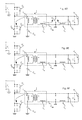
- FIG. 6 shows an electronic half-bridge ZETA converter according to the present description
- FIGS. 7A-7F, 8A-8G, 9A -E, 10 , 11 A- 11 C and 12 show details of embodiments of a driving of the converter of FIG. 6 .
- the electronic ZETA converter of the present description is driven via a half bridge, and therefore this topology is typically called a half-bridge ZETA converter.
- the converter includes a transformer T comprising a primary winding T 1 and a secondary winding T 2 .
- transformer T may be modelled as an ideal transformer with a given turn ratio 1:n, an inductor L M which represents the magnetization inductance of transformer T and an inductor L R which represents the leakage inductance of transformer T.
- connection on the secondary side of the transformer corresponds to a typical ZETA converter, i.e. a diode, two capacitors and an inductor, because the second inductor may be represented by the magnetization inductance of the transformer.
- a first terminal of the primary winding of the transformer is connected to a half bridge, i.e. at the intermediate point between two switches, and therefore such a half bridge is configured to selectively connect such first terminal of the primary winding of transformer to the input voltage or to ground.
- the second terminal of the primary winding of the transformer is connected through at least a capacitor to the input voltage and/or to ground.
- FIG. 6 shows a possible embodiment of an electronic half-bridge ZETA converter.
- converter 12 receives as an input, via two input terminals 110 , a supply signal, such as for instance a DC voltage V in , and supplies as an output, via two output terminals 106 , a regulated voltage V o or a regulated current i o .
- converter 12 includes a half bridge, i.e. two electronic switches S 1 and S 2 which are connected in series between the two input terminals 110 , wherein the switching of electronic switches S 1 and S 2 is driven via a control unit 112 .
- the control unit 112 may be an analogue and/or digital circuit, such as for example a micro-processor which is programmed via a software code.
- such electronic switches S 1 e S 2 are N-MOS transistors or n-channel MOSFETs (Metal-Oxide-Semiconductor Field-Effect Transistors).
- switches S 1 and S 2 have respective capacitances C A1 , C A2 and respective diodes D A1 , D A2 connected in parallel.
- capacitances C A1 and C A2 may represent the intrinsic capacitances of a MOSFET and/or may be implemented with additional capacitors, which are connected in parallel with switches S 1 e S 2 .
- the capacitance of switches S 1 e S 2 may even be remarkably higher than the value 42 pF mentioned in the paper by WU TSAI-FU.
- the sum of capacitances C A1 and C A2 of switches S 1 and S 2 can even reach 1.5 nF.
- the capacitances of switches S 1 and S 2 may reach 100-200 pF, but normally it is necessary to add parallel capacitances, in order to slow down the switching leading edges and to reduce EMIs, and therefore the total capacitance of the node between both switches S 1 e S 2 may reach 1.5 nF, preferably between 200 pF and 1 nF.
- diodes D A1 and D A2 may represent the body diodes of a MOSFET and/or may be implemented through additional diodes.
- a first terminal of primary winding T 1 of transformer T is connected directly to the intermediate point between both electronic switches S 1 and S 2 .
- the second terminal of primary winding T 1 of transformer T is connected via a capacitor C RP to the second input terminal, which represents a first ground GND 1 . Therefore, switches S 1 e S 2 may be used to selectively connect the first terminal of primary winding T 1 of transformer T to voltage V in or to ground GND 1 .
- the ZETA converter includes three branches which are connected in parallel:
- connection on the secondary side of transformer T substantially corresponds to what is shown in FIG. 5 .
- the diagram in FIG. 3 might be used as well.
- the first terminal of secondary winding T 2 of transformer T is connected directly to output 106 , specifically to the first terminal of output 106 .
- the second terminal of secondary winding T 2 is connected through a capacitor C RS (corresponding to capacitor C 1 in FIG. 5 ) to the anode of diode D, wherein the cathode of diode D is connected directly to the first terminal of output 106 .
- the anode of diode D is connected via output inductor L 0 to the second output terminal 106 , which represents a second ground GND 2 , which due to the isolating effect of transformer T is preferably different from ground GND 1 and therefore is denoted with a different ground symbol.
- capacitor C 0 is connected in parallel to output 106 , i.e. directly to the terminals of output 106 .
- the leakage inductance L R of transformer T is shown on the secondary side of transformer T, and the magnetization inductance L M is shown on the primary side of transformer T.
- such inductances L M and L R may also include additional inductors, such as for example an inductor connected in parallel with the primary and/or the secondary winding of transformer T, and/or an inductor connected in series with the primary and/or secondary winding of transformer T.
- the circuit shown in FIG. 6 may be compared with the circuit shown in the paper by WU TSAI-FU.
- switch S 1 instead performs the function of controlling the energy flow from supply V in through the primary side of transformer T.
- the serial connection of capacitors C RS and C RP performs the function of the clamping capacitor Cc described in the paper by WU TSAI-FU.
- FIGS. 7A-7F shows in this respect the wave forms of some signals during these driving modes. Specifically, FIGS. 7A-7F respectively show:
- switch S 1 is closed and switch S 2 remains open.
- diodes D A1 , D A2 and D are open during this operating mode (M 1 ).
- the corresponding equivalent circuit of this driving mode is shown in FIG. 8A .
- switch S 1 is closed at zero voltage (ZVS).
- V T1 V in ⁇ V CRP
- inductance L R is much smaller than inductance L 0 , i.e. L R ⁇ L 0 , and therefore the voltage across inductance L R may be neglected. Therefore, the current I Lo flowing through inductor L 0 corresponds during this mode substantially to:
- I LO ⁇ ( t ) I LO ⁇ ( t ⁇ ⁇ 0 ) + ( V T ⁇ ⁇ 2 + V CRS - V o ) L 0 ⁇ ( t - t ⁇ ⁇ 0 ) ( 4 ) i. e., during this operating mode current I Lo which flows through inductance L 0 increases in a substantially linear way, starting from the value of current I Lo (t 0 ) at time t 0 , which is also visible in FIG. 7D , showing current I DS1 flowing through switch S 1 .
- I LO ⁇ ( t ⁇ ⁇ 1 ) I LO ⁇ ( t ⁇ ⁇ 0 ) + ( V T ⁇ ⁇ 2 + V CRS - V o ) L 0 ⁇ ( t ⁇ ⁇ 1 - t ⁇ ⁇ 0 ) ( 5 )
- diodes D A1 , D A2 and D are still open during this operating mode (M 2 ).
- the corresponding equivalent circuit diagram of this driving mode is shown in FIG. 8B .
- capacitor C A2 is discharged, and voltage V DS2 across switch S 2 falls to zero thanks to that current.
- voltage V DS2 across switch S 2 (and therefore also across capacitance C A2 ) decreases.
- FIG. 8C The corresponding equivalent circuit diagram of this driving mode is shown in FIG. 8C .
- driving signal V G2 closes switch S 2 and, thanks to the fact that voltage V DS2 has been set to zero through diode D A2 , switching is performed at zero voltage.
- the resonant frequency of the current flowing through diode D substantially corresponds to:
- capacitor C RS is charged again during this mode, which is shown in FIG. 7F , and the magnetization current in the magnetization inductance L M increases.
- diode D opens when the current flowing through inductor L 0 equals the resonance current of the resonant circuit, including inductance L R and capacitors C RS and C RP .
- FIGS. 9A-9E which respectively show:
- FIGS. 11A-11C which respectively show:
- switch S 2 is opened, while switch S 1 remains open.
- diodes D A1 , D A2 and D are open in this operating mode (M 6 ).
- the corresponding equivalent circuit diagram of this driving mode is shown in FIG. 8F .
- the dimensioning of components and the switching period should ensure that at time t 5 there is no more orcillation, as shown in FIGS. 9A-9E, 10 and 11A-11C , and current I P through the primary winding has become positive.
- diode D A1 is closed and voltage V DS2 corresponds to input voltage V in , which generates the condition for a zero voltage switching for switch S 1 .
- Diodes D A2 and D stay open during this operation mode (M 7 ).
- the corresponding equivalent circuit diagram of this operating mode is shown in FIG. 8G .
- control unit drives the half-bridge switches with the following steps, which are periodically repeated:
- the duration of the first time interval ⁇ t 1 in which switch S 1 is closed may be controlled so that output voltage V o reaches a desired value, as shown for example in equation (5).
- the duration of the first time interval ⁇ t 1 in which switch S 1 is closed may be controlled so that output voltage V o reaches a desired value, as shown for example in equation (5).
- the output voltage V o which increases or decreases such durations until the supply signal reaches a desired value.
- FIG. 12 shows in this respect a simplified circuit diagram for the operating mode M 6 .
- a capacitor C eq is connected in parallel to switch S 2 .
- a circuit LC including an inductance L P and a capacitance C RP is connected in parallel to switch S 2 .
- the inductor L P represents the magnetization inductance connected in parallel with inductor L 0 (also in this instance neglecting leakage inductance L R );
- the capacitance C eq represents capacitances C A1 e C A2 , and possible other capacitances, wherein capacitance C eq is typically much smaller than capacitance C RP (C eq ⁇ C RP ).
- the missing energy is supplied via inductor L P , which must store at least the following energy:
- I p V in ⁇ D min ⁇ [ ( 1 - D mi ⁇ n ) ⁇ T s ] / 2 L P - ( I o - ⁇ ⁇ ⁇ I L ⁇ ⁇ 0 2 ) ( 13 )
- current I p may also be zero, i.e.
- inductance L 0 is typically sized according to the current ripple ⁇ I L0 which is desired at the output, as if it was a Buck converter.
- duration Tr the current peak in diode D increases.
- duration Tr a reasonable value for duration Tr is:
- Tr 1 4 ⁇ T s ( 18 ) wherein T s is the switching period of the converter, i.e. the duration between two subsequent times t 0 in which switch S 1 is switched on.
- the value of capacitance C R may be calculated as:
- the components may have the following values:
- MOSFETs with a capacity of about 100 pF, wherein an additional capacitor with a capacity up to 400 pF may be connected in parallel with each switch.
- the equivalent capacity C eq in the switching node may therefore be seen as a capacity of about 1000 pF.
- the previously described driving method may therefore operate switches S 1 and S 2 of the half bridge at zero voltage.
- Such a zero voltage switching may also be obtained for a wide interval of possible duty cycles/output voltages.
- the diode of the ZETA converter is switched at zero current.
- the switches of the half bridge may have a reduced size, and also the electromagnetic interferences are reduced.
- the converter may be operated with a fixed switching frequency, wherein the output inductance L 0 may be operated both in the CCM mode and in the DCM mode.
Landscapes
- Engineering & Computer Science (AREA)
- Power Engineering (AREA)
- Dc-Dc Converters (AREA)
Abstract
Description
i D =i C1 +i Lo (1)
-
- the first branch includes the secondary winding of transformer T2 (and therefore magnetization inductance LM) and a capacitor CRS;
- the second branch includes diode D; and
- the third branch includes inductor L0 and a capacitor C0, wherein load RL, i.e.
output 106, is connected in parallel with capacitor C0.
V T1 =V in −V CRP (2)
V T2 =V T1 (3)
i. e., during this operating mode current ILo which flows through inductance L0 increases in a substantially linear way, starting from the value of current ILo(t0) at time t0, which is also visible in
I P =I LM +I L0 (6)
I D =I CRS +I Lo (7)
wherein CR corresponds to capacitance CRP connected in series with capacitance CRS.
V T1 =V CRP =V T2 <V CRS
and, neglecting the voltage across leakage inductance LR, voltage VD across the diode is:
V D =V CRS −V T2<0
V T1 =V CRP =V T2 =V CRS
and therefore the voltage across diode D is zero:
V D=0
-
- during a first time interval Δt1 switch S1 is closed and switch S2 is open (times t0-t1);
- during a second time interval Δt2 switch S1 is open and switch S2 is open (times t1-t3); wherein,
- during said second time interval Δt2, capacitance CA1 associated to switch S2 is charged and capacitance CA2 associated to switch S2 is discharged, creating the condition for a zero voltage switching of switch S2;
- during a third time interval Δt3 switch S1 is open and switch S2 is closed (times t3-t5); wherein, during said third time interval Δt3, the magnetization current of the magnetization inductance increases and diode D of the ZETA converter is switched off at zero current; and
- during a fourth time interval Δt4 switch S1 is open and switch S2 is open (times t5-t0); wherein, during such a time interval Δt4, capacitance CA2 associated to switch S2 is charged and capacitance CA1 associated to switch S1 is discharged, creating the condition for a switching at zero voltage of switch S1.
Δt3=Ts−Δt1−Δt2−Δt4 (9)
wherein Ts is the duration of a switching period which is constant.
V DS2,min=2·V in ·D min (11)
wherein Dmin represents the minimum duty cycle, i.e. the duty cycle for the smallest ratio between output voltage Vo and input voltage Vin.
wherein current Ip corresponds to:
and, as a consequence, the value of inductance LP may be calculated as:
wherein:
Tr=π√{square root over (L R C R)}≦(1−D max)T s (17)
wherein Dmax is the maximum duty cycle.
wherein Ts is the switching period of the converter, i.e. the duration between two subsequent times t0 in which switch S1 is switched on.
-
- a capacitance Ceq up to 1.5 nF;
- an inductance Lp between 200 pH and 3 mH.
Claims (10)
Applications Claiming Priority (4)
| Application Number | Priority Date | Filing Date | Title |
|---|---|---|---|
| ITTO2013A0771 | 2013-09-25 | ||
| ITTO20130771 | 2013-09-25 | ||
| ITTO2013A000771 | 2013-09-25 | ||
| PCT/IB2014/064657 WO2015044846A2 (en) | 2013-09-25 | 2014-09-19 | Electronic half-bridge zeta converter and related method for operating an electronic half-bridge zeta converter and method for designing an electronic half- bridge zeta converter |
Publications (2)
| Publication Number | Publication Date |
|---|---|
| US20160211759A1 US20160211759A1 (en) | 2016-07-21 |
| US9831784B2 true US9831784B2 (en) | 2017-11-28 |
Family
ID=49640072
Family Applications (1)
| Application Number | Title | Priority Date | Filing Date |
|---|---|---|---|
| US15/024,360 Active US9831784B2 (en) | 2013-09-25 | 2014-09-19 | Electronic resonant and insulated half-bridge zeta converter |
Country Status (4)
| Country | Link |
|---|---|
| US (1) | US9831784B2 (en) |
| EP (1) | EP3050400B1 (en) |
| CN (1) | CN105580497B (en) |
| WO (1) | WO2015044846A2 (en) |
Families Citing this family (17)
| Publication number | Priority date | Publication date | Assignee | Title |
|---|---|---|---|---|
| US9627979B2 (en) * | 2014-10-03 | 2017-04-18 | Bombardier Transportation Gmbh | Dual mode DC-DC converter |
| EP3160028B1 (en) * | 2015-09-28 | 2021-08-04 | OSRAM GmbH | Electronic converter and related method of operating an electronic converter |
| US10770980B2 (en) | 2015-10-06 | 2020-09-08 | Osram Gmbh | Electronic converter and related method of operating an electronic converter |
| EP3365967B1 (en) | 2015-10-23 | 2019-08-21 | OSRAM GmbH | Electronic converter and related method of operating an electronic converter |
| DE102017204907A1 (en) | 2017-03-23 | 2018-09-27 | Osram Gmbh | Method and clocked converter for operating an input power quickly following light sources |
| EP3402060B1 (en) * | 2017-05-09 | 2019-10-02 | OSRAM GmbH | Electronic converter and related method of operating an electronic converter |
| WO2019211286A1 (en) * | 2018-05-01 | 2019-11-07 | Danmarks Tekniske Universitet | Resonant type power factor correction ac-dc converter and method for operating a resonant type power factor correction ac-dc converter |
| CN110118903B (en) * | 2019-04-19 | 2021-07-23 | 清华大学 | Equivalent full power test circuit and control method of DC port of power electronic transformer |
| CN112117905B (en) | 2019-06-20 | 2021-12-21 | 东南大学 | Control system and method of active clamp flyback converter |
| WO2021212322A1 (en) * | 2020-04-21 | 2021-10-28 | Telefonaktiebolaget Lm Ericsson (Publ) | A dc-to-dc convertor |
| CN111556616B (en) * | 2020-06-02 | 2021-06-22 | 福州大学 | A single-stage bridgeless boost Cuk resonant LED drive circuit |
| CN111969877B (en) * | 2020-06-23 | 2021-07-02 | 湖南大学 | A control method and device for a half-bridge inverter |
| IT202000015232A1 (en) | 2020-06-24 | 2021-12-24 | St Microelectronics Srl | SWITCHING CONVERTER |
| TWI771882B (en) * | 2021-01-27 | 2022-07-21 | 群光電能科技股份有限公司 | Power converter device and driving method |
| US11962247B2 (en) * | 2021-02-25 | 2024-04-16 | Richtek Technology Corporation | Resonant half-bridge flyback power converter with skipping cycles and control method thereof |
| CN113346743B (en) * | 2021-06-24 | 2022-05-20 | 江苏大学 | Non-isolated high-gain direct current converter |
| EP4418518A1 (en) * | 2023-02-14 | 2024-08-21 | Hamilton Sundstrand Corporation | Three-level zeta asymmetrical half-bridge |
Citations (10)
| Publication number | Priority date | Publication date | Assignee | Title |
|---|---|---|---|---|
| US5325283A (en) * | 1992-06-08 | 1994-06-28 | Center For Innovative Technology | Novel zero-voltage-switching family of isolated converters |
| US5684688A (en) * | 1996-06-24 | 1997-11-04 | Reliance Electric Industrial Company | Soft switching three-level inverter |
| US5757626A (en) * | 1996-06-21 | 1998-05-26 | Delta Electronics Inc. | Single-stage, single-switch, islolated power-supply technique with input-current shaping and fast output-voltage regulation |
| US5790389A (en) * | 1996-05-31 | 1998-08-04 | Virginia Power Technologies, Inc. | Consolidated soft-switching AC/DC converters |
| US6272027B1 (en) * | 2000-07-28 | 2001-08-07 | Simon Fraidlin | AC active clamp for isolated power factor corrector and method of operating the same |
| US20070230228A1 (en) * | 2006-03-31 | 2007-10-04 | Hong Mao | Zero-voltage-switching DC-DC converters with synchronous rectifiers |
| US20100165669A1 (en) * | 2008-12-31 | 2010-07-01 | Macroblock, Inc. | Single-stage isolated high power factor ac/dc converter with leakage inductor energy recovery function |
| US20100208499A1 (en) | 2007-07-04 | 2010-08-19 | Nxp B.V. | Standby operation of a resonant power converter |
| US20120230059A1 (en) | 2011-03-11 | 2012-09-13 | Stmicroelectronics S.R.L. | Device for avoiding hard switching in resonant converter and related method |
| US20140092643A1 (en) * | 2012-09-28 | 2014-04-03 | Osram Gmbh | Electronic converter, and related lighting system and method of operating an electronic converter |
-
2014
- 2014-09-19 EP EP14789391.1A patent/EP3050400B1/en active Active
- 2014-09-19 WO PCT/IB2014/064657 patent/WO2015044846A2/en not_active Ceased
- 2014-09-19 CN CN201480052864.6A patent/CN105580497B/en not_active Expired - Fee Related
- 2014-09-19 US US15/024,360 patent/US9831784B2/en active Active
Patent Citations (10)
| Publication number | Priority date | Publication date | Assignee | Title |
|---|---|---|---|---|
| US5325283A (en) * | 1992-06-08 | 1994-06-28 | Center For Innovative Technology | Novel zero-voltage-switching family of isolated converters |
| US5790389A (en) * | 1996-05-31 | 1998-08-04 | Virginia Power Technologies, Inc. | Consolidated soft-switching AC/DC converters |
| US5757626A (en) * | 1996-06-21 | 1998-05-26 | Delta Electronics Inc. | Single-stage, single-switch, islolated power-supply technique with input-current shaping and fast output-voltage regulation |
| US5684688A (en) * | 1996-06-24 | 1997-11-04 | Reliance Electric Industrial Company | Soft switching three-level inverter |
| US6272027B1 (en) * | 2000-07-28 | 2001-08-07 | Simon Fraidlin | AC active clamp for isolated power factor corrector and method of operating the same |
| US20070230228A1 (en) * | 2006-03-31 | 2007-10-04 | Hong Mao | Zero-voltage-switching DC-DC converters with synchronous rectifiers |
| US20100208499A1 (en) | 2007-07-04 | 2010-08-19 | Nxp B.V. | Standby operation of a resonant power converter |
| US20100165669A1 (en) * | 2008-12-31 | 2010-07-01 | Macroblock, Inc. | Single-stage isolated high power factor ac/dc converter with leakage inductor energy recovery function |
| US20120230059A1 (en) | 2011-03-11 | 2012-09-13 | Stmicroelectronics S.R.L. | Device for avoiding hard switching in resonant converter and related method |
| US20140092643A1 (en) * | 2012-09-28 | 2014-04-03 | Osram Gmbh | Electronic converter, and related lighting system and method of operating an electronic converter |
Non-Patent Citations (4)
| Title |
|---|
| Bor-Ren Lin and Fang-Yu Hsieh, IEEE vol. 54 No. 5 Oct. 2007, Soft-Switching Zeta-Flyback Converter with a Buck-Boost Type of Active Clamp. * |
| Huai Wei et al: "Comparison of basic converter topologies for power factor correction" SOUTHEASTCON '98; Apr. 24, 1998; pp. 348-353. |
| International Search Report based on application No. PCT/IB2014/064657 (6 pages) dated Mar. 20, 2015 (for reference purpose only). |
| Tsai-Fu et al.: "Design optimization for asymmetrical ZVS-PWM zeta converter"; IEEE Transactions on Aerospace and Electronic Systems; Apr. 1, 2003; pp. 521-532. |
Also Published As
| Publication number | Publication date |
|---|---|
| CN105580497A (en) | 2016-05-11 |
| EP3050400B1 (en) | 2019-01-02 |
| US20160211759A1 (en) | 2016-07-21 |
| WO2015044846A3 (en) | 2015-06-11 |
| EP3050400A2 (en) | 2016-08-03 |
| CN105580497B (en) | 2018-03-16 |
| WO2015044846A2 (en) | 2015-04-02 |
Similar Documents
| Publication | Publication Date | Title |
|---|---|---|
| US9831784B2 (en) | Electronic resonant and insulated half-bridge zeta converter | |
| EP2713488B1 (en) | Electronic converter, and related lighting system and method of operating an electronic converter | |
| US8233292B2 (en) | Controllers, systems and methods for controlling power of light sources | |
| EP2536013B1 (en) | A cascade boost and inverting buck converter | |
| US8837174B2 (en) | Switching power-supply apparatus including switching elements having a low threshold voltage | |
| US11437924B2 (en) | Switching power supply circuit | |
| US9210749B2 (en) | Single switch driver device having LC filter for driving an LED unit | |
| US6834002B2 (en) | Power factor correction circuit | |
| US8188617B2 (en) | Current balancing apparatus, current balancing method, and power supply apparatus | |
| US9544956B2 (en) | Two-stage multichannel LED driver with CLL resonant circuit | |
| US11582843B1 (en) | Average current control circuit and method | |
| EP3365967B1 (en) | Electronic converter and related method of operating an electronic converter | |
| US10770980B2 (en) | Electronic converter and related method of operating an electronic converter | |
| JP5547849B2 (en) | DC power supply circuit | |
| US11622429B1 (en) | QR-operated switching converter current driver | |
| EP3160028B1 (en) | Electronic converter and related method of operating an electronic converter | |
| US10243474B2 (en) | Electronic converter and related method of operating an electronic converter | |
| JP6791486B2 (en) | Light emitting element drive device and its drive method | |
| Ongaro et al. | ZVS isolated active clamp sepic converter for high power LED applications | |
| JP5644089B2 (en) | Multi-output switching power supply | |
| JP2013051860A (en) | Power-supply circuit |
Legal Events
| Date | Code | Title | Description |
|---|---|---|---|
| AS | Assignment |
Owner name: OSRAM GMBH, GERMANY Free format text: ASSIGNMENT OF ASSIGNORS INTEREST;ASSIGNOR:LUCCATO, DANIELE;REEL/FRAME:038087/0739 Effective date: 20160202 |
|
| STCF | Information on status: patent grant |
Free format text: PATENTED CASE |
|
| CC | Certificate of correction | ||
| MAFP | Maintenance fee payment |
Free format text: PAYMENT OF MAINTENANCE FEE, 4TH YEAR, LARGE ENTITY (ORIGINAL EVENT CODE: M1551); ENTITY STATUS OF PATENT OWNER: LARGE ENTITY Year of fee payment: 4 |
|
| AS | Assignment |
Owner name: ACUITY BRANDS LIGHTING, INC., GEORGIA Free format text: ASSIGNMENT OF ASSIGNORS INTEREST;ASSIGNOR:OSRAM GMBH;REEL/FRAME:058689/0898 Effective date: 20210701 |
|
| AS | Assignment |
Owner name: ABL IP HOLDING LLC, GEORGIA Free format text: ASSIGNMENT OF ASSIGNORS INTEREST;ASSIGNOR:ACUITY BRANDS LIGHTING, INC.;REEL/FRAME:059220/0139 Effective date: 20220214 |
|
| MAFP | Maintenance fee payment |
Free format text: PAYMENT OF MAINTENANCE FEE, 8TH YEAR, LARGE ENTITY (ORIGINAL EVENT CODE: M1552); ENTITY STATUS OF PATENT OWNER: LARGE ENTITY Year of fee payment: 8 |