US9831780B2 - Buck-boost converter and method for controlling buck-boost converter - Google Patents
Buck-boost converter and method for controlling buck-boost converter Download PDFInfo
- Publication number
- US9831780B2 US9831780B2 US15/209,750 US201615209750A US9831780B2 US 9831780 B2 US9831780 B2 US 9831780B2 US 201615209750 A US201615209750 A US 201615209750A US 9831780 B2 US9831780 B2 US 9831780B2
- Authority
- US
- United States
- Prior art keywords
- switch
- buck
- mode
- boost converter
- boost
- Prior art date
- Legal status (The legal status is an assumption and is not a legal conclusion. Google has not performed a legal analysis and makes no representation as to the accuracy of the status listed.)
- Expired - Fee Related
Links
Images


Classifications
-
- H—ELECTRICITY
- H02—GENERATION; CONVERSION OR DISTRIBUTION OF ELECTRIC POWER
- H02M—APPARATUS FOR CONVERSION BETWEEN AC AND AC, BETWEEN AC AND DC, OR BETWEEN DC AND DC, AND FOR USE WITH MAINS OR SIMILAR POWER SUPPLY SYSTEMS; CONVERSION OF DC OR AC INPUT POWER INTO SURGE OUTPUT POWER; CONTROL OR REGULATION THEREOF
- H02M3/00—Conversion of DC power input into DC power output
- H02M3/02—Conversion of DC power input into DC power output without intermediate conversion into AC
- H02M3/04—Conversion of DC power input into DC power output without intermediate conversion into AC by static converters
- H02M3/10—Conversion of DC power input into DC power output without intermediate conversion into AC by static converters using discharge tubes with control electrode or semiconductor devices with control electrode
- H02M3/145—Conversion of DC power input into DC power output without intermediate conversion into AC by static converters using discharge tubes with control electrode or semiconductor devices with control electrode using devices of a triode or transistor type requiring continuous application of a control signal
- H02M3/155—Conversion of DC power input into DC power output without intermediate conversion into AC by static converters using discharge tubes with control electrode or semiconductor devices with control electrode using devices of a triode or transistor type requiring continuous application of a control signal using semiconductor devices only
- H02M3/156—Conversion of DC power input into DC power output without intermediate conversion into AC by static converters using discharge tubes with control electrode or semiconductor devices with control electrode using devices of a triode or transistor type requiring continuous application of a control signal using semiconductor devices only with automatic control of output voltage or current, e.g. switching regulators
- H02M3/158—Conversion of DC power input into DC power output without intermediate conversion into AC by static converters using discharge tubes with control electrode or semiconductor devices with control electrode using devices of a triode or transistor type requiring continuous application of a control signal using semiconductor devices only with automatic control of output voltage or current, e.g. switching regulators including plural semiconductor devices as final control devices for a single load
- H02M3/1582—Buck-boost converters
-
- G—PHYSICS
- G05—CONTROLLING; REGULATING
- G05F—SYSTEMS FOR REGULATING ELECTRIC OR MAGNETIC VARIABLES
- G05F1/00—Automatic systems in which deviations of an electric quantity from one or more predetermined values are detected at the output of the system and fed back to a device within the system to restore the detected quantity to its predetermined value or values, i.e. retroactive systems
- G05F1/10—Regulating voltage or current
- G05F1/46—Regulating voltage or current wherein the variable actually regulated by the final control device is DC
- G05F1/62—Regulating voltage or current wherein the variable actually regulated by the final control device is DC using bucking or boosting DC sources
-
- H—ELECTRICITY
- H02—GENERATION; CONVERSION OR DISTRIBUTION OF ELECTRIC POWER
- H02M—APPARATUS FOR CONVERSION BETWEEN AC AND AC, BETWEEN AC AND DC, OR BETWEEN DC AND DC, AND FOR USE WITH MAINS OR SIMILAR POWER SUPPLY SYSTEMS; CONVERSION OF DC OR AC INPUT POWER INTO SURGE OUTPUT POWER; CONTROL OR REGULATION THEREOF
- H02M1/00—Details of apparatus for conversion
- H02M1/0048—Circuits or arrangements for reducing losses
- H02M1/0054—Transistor switching losses
-
- H02M2001/0054—
-
- H—ELECTRICITY
- H02—GENERATION; CONVERSION OR DISTRIBUTION OF ELECTRIC POWER
- H02M—APPARATUS FOR CONVERSION BETWEEN AC AND AC, BETWEEN AC AND DC, OR BETWEEN DC AND DC, AND FOR USE WITH MAINS OR SIMILAR POWER SUPPLY SYSTEMS; CONVERSION OF DC OR AC INPUT POWER INTO SURGE OUTPUT POWER; CONTROL OR REGULATION THEREOF
- H02M3/00—Conversion of DC power input into DC power output
- H02M3/02—Conversion of DC power input into DC power output without intermediate conversion into AC
- H02M3/04—Conversion of DC power input into DC power output without intermediate conversion into AC by static converters
- H02M3/10—Conversion of DC power input into DC power output without intermediate conversion into AC by static converters using discharge tubes with control electrode or semiconductor devices with control electrode
- H02M3/145—Conversion of DC power input into DC power output without intermediate conversion into AC by static converters using discharge tubes with control electrode or semiconductor devices with control electrode using devices of a triode or transistor type requiring continuous application of a control signal
- H02M3/155—Conversion of DC power input into DC power output without intermediate conversion into AC by static converters using discharge tubes with control electrode or semiconductor devices with control electrode using devices of a triode or transistor type requiring continuous application of a control signal using semiconductor devices only
- H02M3/156—Conversion of DC power input into DC power output without intermediate conversion into AC by static converters using discharge tubes with control electrode or semiconductor devices with control electrode using devices of a triode or transistor type requiring continuous application of a control signal using semiconductor devices only with automatic control of output voltage or current, e.g. switching regulators
- H02M3/158—Conversion of DC power input into DC power output without intermediate conversion into AC by static converters using discharge tubes with control electrode or semiconductor devices with control electrode using devices of a triode or transistor type requiring continuous application of a control signal using semiconductor devices only with automatic control of output voltage or current, e.g. switching regulators including plural semiconductor devices as final control devices for a single load
- H02M3/1584—Conversion of DC power input into DC power output without intermediate conversion into AC by static converters using discharge tubes with control electrode or semiconductor devices with control electrode using devices of a triode or transistor type requiring continuous application of a control signal using semiconductor devices only with automatic control of output voltage or current, e.g. switching regulators including plural semiconductor devices as final control devices for a single load with a plurality of power processing stages connected in parallel
-
- H—ELECTRICITY
- H02—GENERATION; CONVERSION OR DISTRIBUTION OF ELECTRIC POWER
- H02M—APPARATUS FOR CONVERSION BETWEEN AC AND AC, BETWEEN AC AND DC, OR BETWEEN DC AND DC, AND FOR USE WITH MAINS OR SIMILAR POWER SUPPLY SYSTEMS; CONVERSION OF DC OR AC INPUT POWER INTO SURGE OUTPUT POWER; CONTROL OR REGULATION THEREOF
- H02M3/00—Conversion of DC power input into DC power output
- H02M3/02—Conversion of DC power input into DC power output without intermediate conversion into AC
- H02M3/04—Conversion of DC power input into DC power output without intermediate conversion into AC by static converters
- H02M3/10—Conversion of DC power input into DC power output without intermediate conversion into AC by static converters using discharge tubes with control electrode or semiconductor devices with control electrode
- H02M3/145—Conversion of DC power input into DC power output without intermediate conversion into AC by static converters using discharge tubes with control electrode or semiconductor devices with control electrode using devices of a triode or transistor type requiring continuous application of a control signal
- H02M3/155—Conversion of DC power input into DC power output without intermediate conversion into AC by static converters using discharge tubes with control electrode or semiconductor devices with control electrode using devices of a triode or transistor type requiring continuous application of a control signal using semiconductor devices only
- H02M3/156—Conversion of DC power input into DC power output without intermediate conversion into AC by static converters using discharge tubes with control electrode or semiconductor devices with control electrode using devices of a triode or transistor type requiring continuous application of a control signal using semiconductor devices only with automatic control of output voltage or current, e.g. switching regulators
- H02M3/158—Conversion of DC power input into DC power output without intermediate conversion into AC by static converters using discharge tubes with control electrode or semiconductor devices with control electrode using devices of a triode or transistor type requiring continuous application of a control signal using semiconductor devices only with automatic control of output voltage or current, e.g. switching regulators including plural semiconductor devices as final control devices for a single load
- H02M3/1588—Conversion of DC power input into DC power output without intermediate conversion into AC by static converters using discharge tubes with control electrode or semiconductor devices with control electrode using devices of a triode or transistor type requiring continuous application of a control signal using semiconductor devices only with automatic control of output voltage or current, e.g. switching regulators including plural semiconductor devices as final control devices for a single load comprising at least one synchronous rectifier element
-
- Y—GENERAL TAGGING OF NEW TECHNOLOGICAL DEVELOPMENTS; GENERAL TAGGING OF CROSS-SECTIONAL TECHNOLOGIES SPANNING OVER SEVERAL SECTIONS OF THE IPC; TECHNICAL SUBJECTS COVERED BY FORMER USPC CROSS-REFERENCE ART COLLECTIONS [XRACs] AND DIGESTS
- Y02—TECHNOLOGIES OR APPLICATIONS FOR MITIGATION OR ADAPTATION AGAINST CLIMATE CHANGE
- Y02B—CLIMATE CHANGE MITIGATION TECHNOLOGIES RELATED TO BUILDINGS, e.g. HOUSING, HOUSE APPLIANCES OR RELATED END-USER APPLICATIONS
- Y02B70/00—Technologies for an efficient end-user side electric power management and consumption
- Y02B70/10—Technologies improving the efficiency by using switched-mode power supplies [SMPS], i.e. efficient power electronics conversion e.g. power factor correction or reduction of losses in power supplies or efficient standby modes
-
- Y02B70/1491—
Definitions
- a buck-boost converter is generally used in an electronic device to provide a stable output voltage while receiving an input voltage with wide range.
- the U.S. Pat. Nos. 6,166,527, 5,402,060 and 7,692,416 disclose the techniques about the buck-boost converter, however, in the buck-boost switching regulator disclosed by U.S. Pat. No. 6,166,527 and the buck-boost converter disclosed by U.S. Pat. No. 5,402,060, the switch connected to the output voltage cannot conduct both high voltage and low voltage (close to zero/ground), which may decrease the efficiency; and in the voltage up-and-down DC-DC converter disclosed by U.S. Pat. No. 7,692,416, two transistors of the transmission gate connected to the output voltage are controlled by the related signals in the buck mode and the boost mode, and the switching loss may be increased in this operation.
- a buck-boost converter for receiving an input voltage to generate an output voltage.
- the buck-boost converter comprises an inductor, a first switch, a second switch, a third switch, a fourth switch and a fifth switch, wherein the first switch is coupled between the input voltage and a first terminal of the inductor, the second switch is coupled between a reference voltage and the first terminal of the inductor, the third switch is coupled between the output voltage and a second terminal of the inductor, the fourth switch is coupled between the reference voltage and the second terminal of the inductor, and the fifth switch is connected in parallel with the third switch.
- each of the first switch and the second switch is turned on and off alternately; when the buck-boost converter operates in a boost mode, each of the third switch and the fourth switch is turned on and off alternately; and the fifth switch is controlled to be on or off by referring to a mode control signal that represents the buck mode or the boost mode.
- a method for controlling a buck-boost converter comprising: when the buck-boost converter operates in a buck mode, controlling each of the first switch and the second switch to turn on and off alternately; when the buck-boost converter operates in a boost mode, controlling each the third switch and the fourth switch to turn on and off alternately;
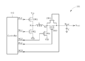
- FIG. 1 is a diagram illustrating a buck-boost converter according to one embodiment of the present invention.
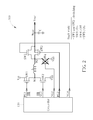
- FIG. 2 is a diagram illustrating the buck mode of the buck-boost converter according to one embodiment of the present invention.
- FIG. 3 is a diagram illustrating the boost mode of the buck-boost converter according to one embodiment of the present invention.
- FIG. 4 is a diagram illustrating the generation of the control signal NG 3 according to a first embodiment of the present invention.
- FIG. 5 is a diagram illustrating the generation of the control signal NG 3 according to a second embodiment of the present invention.
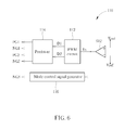
- FIG. 6 is a diagram illustrating the generation of the control signal NG 3 according to a third embodiment of the present invention.
- FIG. 7 is a diagram illustrating the control circuit according to another embodiment of the present invention.
- FIG. 8 shows a timing diagram of the signals shown in FIG. 7 when the buck-boost converter operates from the buck mode to the boost mode according to one embodiment of the present invention.
- FIG. 9 shows a timing diagram of the signals shown in FIG. 7 when the buck-boost converter operates from the buck mode to the boost mode according to another embodiment of the present invention.
- FIG. 1 is a diagram illustrating a buck-boost converter 100 according to one embodiment of the present invention.
- the buck-boost converter 100 is arranged to receive an input voltage Vin from a battery or any other supply voltage provider to generate a stable output voltage Vout at an output node Nout, and the buck-boost converter 100 comprises five switches SW 1 -SW 5 , an inductor L, and a capacitor C, where the switch SW 1 is implemented by a PMOS and coupled between the input voltage Vin and a first terminal N 1 of the inductor L, the switch SW 2 is implemented by an NMOS and coupled between the first terminal N 1 of the inductor L and a reference voltage VSS (in this embodiment, the reference voltage is a ground voltage), the SW 3 is implemented by a PMOS and coupled between the output voltage Vout and a second terminal N 2 of the inductor L, the SW 4 is implemented by an NMOS and coupled between the second terminal N 2 of the inductor L
- the buck-boost converter 100 further comprises a control circuit 110 to generate five control signals PG 1 , NG 1 , PG 2 , NG 2 and NG 3 to control the switches SW 1 -SW 5 , respectively.
- the control circuit 110 can determine a mode (buck mode or boost mode) of the buck-boost converter 100 according to information within the buck-boost converter 100 , and control circuit 110 generates the control signals PG 1 , NG 1 , PG 2 , NG 2 and NG 3 according to the mode of the buck-boost converter 100 .
- control circuit 110 may determine the mode of the buck-boost converter 100 according to at least one of the input voltage Vin, the output voltage Vout, a duty cycle of a portion of the control signals PG 1 , NG 1 , PG 2 , NG 2 and NG 3 , or any suitable control signal within the control circuit 110 . Details of the determination of the mode are described in the following figures.
- FIG. 2 is a diagram illustrating the buck mode of the buck-boost converter 100 according to one embodiment of the present invention.
- the control circuit 110 when the buck-boost converter 100 operates in the buck mode, the control circuit 110 generates the control signals PG 1 and NG 1 to control the switches SW 1 and SW 2 , respectively, to make the switches SW 1 and SW 2 to turn on and off alternately, and the switches SW 1 and SW 2 are not turned on simultaneously.
- the control circuit 110 further generates the control signal PG 2 to always turn on the switch SW 3 , and further generates the control signal NG 2 to always turn off the switch SW 4 , and generates the control signal NG 3 to turn on the switch SW 5 .
- the switches SW 3 and SW 5 are turned on simultaneously, and because the NMOS switch can conduct low voltage (close to zero/ground voltage), so the output node Nout is allowed to receive the low voltage (close to zero/ground voltage), and the efficiency of the buck-boost converter 100 operated in the buck mode can be improved.
- FIG. 3 is a diagram illustrating the boost mode of the buck-boost converter 100 according to one embodiment of the present invention.
- the control circuit 110 when the buck-boost converter 100 operates in the boost mode, the control circuit 110 generates the control signal PG 1 to always turn on the switch SW 1 , and generates the control signal NG 1 to always turn off the switch SW 2 , and further generates the control signals PG 2 and NG 2 to control the switches SW 3 and SW 4 , respectively, to make the switches SW 3 and SW 4 to turn on and off alternately, and the switches SW 3 and SW 4 are not turned on simultaneously.
- the control circuit 110 generates the mode control signal NG 3 to turn off the switch SW 5 .
- the PMOS switch SW 3 can conduct the high voltage and is capable of doing the work efficiently, so the switch SW 5 is turned off to reduce the switching loss.
- control circuit 110 may compare the input voltage Vin and the output voltage Vout to generate the mode control signal NG 3 .
- the switch SW 5 is turned on by the mode control signal NG 3 ; and when the input voltage is less than the output voltage Vout, it is determined that the buck-boost converter 100 operates in the boost mode, and the switch SW 5 is turned off by the mode control signal NG 3 .
- control circuit 110 may determines the mode of the buck-boost converter 100 according to information generated based on the input voltage Vin and the output voltage Vout, for example, Vin/Vout, Vout/Vin, Vin/Vref or Vout/Vref, where “Vref” may be any suitable value.
- the control circuit 110 comprises a pulse-width modulation (PWM) circuit 112 , a predriver 114 and a mode control signal generator 116 .
- the PWM circuit 112 is arranged to generate a duty cycle information D 1 corresponding to the control signals PG 1 and NG 1 , and to generate a duty cycle information D 2 corresponding to the control signals PG 2 and NG 2 ; and the predriver 114 is arranged to generate the control signals PG 1 , NG 1 , PG 2 and NG 2 according to the duty cycle information D 1 and D 2 .
- PWM pulse-width modulation
- the mode control signal generator 116 is arranged to generate the mode control signal NG 3 according to a current mode of the buck-boost converter 100 , where the current mode may be a buck mode or a boost mode.
- the mode control signal generator 116 may refer to at least one of the duty cycle information D 1 and D 2 and the control signals PG 1 , PG 2 , NG 1 and NG 2 to generate the control signal NG 3 .
- the mode control signal generator 116 may perform some logical calculations upon at least one of the control signals PG 1 , PG 2 , NG 1 and NG 2 to generate the mode control signal NG 3 .
- the mode control signal generator 116 can refer to the duty cycle of the control signal PG 1 to determine the current mode of the buck-boost converter 100 to generate the control signal NG 3 .
- the mode control signal generator 116 can refer to the duty cycle of the control signal PG 2 to determine the current mode of the buck-boost converter 100 to generate the control signal NG 3 .
- FIG. 6 is a diagram illustrating the generation of the mode control signal NG 3 according to a third embodiment of the present invention.
- the buck-boost converter 100 further comprises a comparator 602 , and the comparator 602 compares the output voltage Vout and a reference voltage to generate a comparison result Vs.
- the comparison result Vs is proportional to the output voltage Vout (assuming that the input voltage does not change), therefore, when the comparison result Vs continuously increases to reach a threshold, the mode control signal generator 116 can determine that the buck-boost converter 100 operates in the boost mode, and the control signal generator 116 generates the mode control signal NG 3 to turn off the switch SW 5 .
- FIG. 7 is a diagram illustrating the control circuit 110 according to another embodiment of the present invention.
- the control circuit 110 comprises a compensation circuit 710 , a PWM controller 720 and a pre-driver 730 .
- the compensation circuit 710 is arranged to provide several reference voltages to the PWM controller 720 , and the PWM controller 720 generates duty cycle information and mode control information to the pre-driver 730 to generate the control signals PG 1 , NG 1 , PG 2 , NG 2 and NG 3 .
- the compensation circuit 710 comprises a feedback network 711 , a reference signal generator 712 , a compensator 713 and a comparator 714 .
- the reference signal generator 712 is arranged to generate a reference voltage Vset to a positive input terminal of the comparator 714 , and further generates a reference voltage Vr 1 to the PWM controller 720 .
- the comparator 714 compares the reference voltage with the output voltage Vout to generate an error signal VEA to the PWM controller 720 .
- the PWM controller 720 comprises a circuit 722 , two comparator 723 and 724 , a hysteresis comparator module 728 and a PWM logic 726 .
- the circuit 722 comprises a first ramp signal generator 731 , a second ramp signal generator 732 , an input voltage comparator 733 and a ramp setting circuit 734 .
- the first ramp signal generator 731 is arranged to generate a ramp signal Ramp 1 to the comparator 723 , and the comparator 723 compares the ramp signal Ramp 1 with the error signal VEA to generate a first PWM signal PWM 1 ; and the second ramp signal generator 732 is arranged to generate a ramp signal Ramp 2 to the comparator 724 , and the comparator 724 compares the ramp signal Ramp 2 with the error signal VEA to generate a second PWM signal PWM 2 .
- the input voltage comparator 733 is arranged to compare the input voltage Vin with a setup output voltage to selectively force the mode switching.
- the ramp setting circuit 734 is controlled to provide hysteresis thresholds Hys_Vth (e.g.
- a high threshold Vthh and a low threshold Vthn to the hysteresis comparator module 728
- a hysteresis comparator 741 compares the error signal VEA with the reference signal Vr 1 to generate a mode signal Mode 1
- a hysteresis comparator 742 compares the reference signal Vset with the supply voltage VDD to generate a mode signal Mode 2 according to the hysteresis thresholds Hys_Vth.
- the PWM logic 726 generates the duty cycle information Data 1 and Data 2 of the control signals PG 1 , NG 1 , PG 2 and NG 2 and a mode signal to the pre-driver 730 according to at least the first PWM signal PWM 1 , the second PWM signal PWM 2 , the mode signal Mode 1 and the mode signal Mode 2 .
- the duty cycle information D 1 corresponding to the control signals PG 1 and NG 1 and the duty cycle information D 2 corresponding to the control signals PG 2 and NG 2 .
- a clock reset signal CK_RST is arranged to avoid the comparator saturation issue and to improve the comparator response time.
- the PWM logic 726 may control the buck-boost operations to have several transition modes when the mode switching occurs.
- FIG. 8 shows a timing diagram of the signals shown in FIG. 7 when the buck-boost converter 100 operates from the buck mode to the boost mode according to one embodiment of the present invention.
- the PWM logic 726 still outputs the duty cycle information Data 1 until the mode signal BCK_mode goes low (i.e. the buck-boost converter 100 enters the boost mode), and then PWM logic 726 outputs the duty cycle information Data 2 .
- the buck mode and the boost mode are roaming and two of the switches SW 1 -SW 5 shown in FIG. 1 are toggling.
- a seamless control may be applied, and during the transition when the buck-boost converter 100 is switching from the buck mode to the boost mode, the four switches SW 1 -SW 4 are all toggling during this period.
- FIG. 9 shows a timing diagram of the signals shown in FIG. 7 when the buck-boost converter 100 operates from the buck mode to the boost mode according to another embodiment of the present invention.
- the comparison result for the low threshold Vthn of the hysteresis window is high
- the PWM logic 726 stops generating the duty cycle information Data 1
- the mode signal BCK_mode goes low (i.e. the buck-boost converter 100 enters the boost mode)
- the PWM logic 726 starts to output the duty cycle information Data 2 . That is, during the transition when the buck-boost converter 100 is switching from the buck mode to the boost mode, a bypass period is existed.
- an additional switch SW 5 is provided to conduct the low voltage (close to zero/ground voltage) to make the buck-boost converter to work efficiently in the buck mode.
- the switch SW 5 is turned off when the buck-boost converter operates in the boost mode to reduce the switching loss. Therefore, buck-boost converter may improve both the efficiency and switching loss, to solve the above-mentioned problem.
Landscapes
- Engineering & Computer Science (AREA)
- Power Engineering (AREA)
- Dc-Dc Converters (AREA)
Abstract
Description
Claims (12)
Priority Applications (3)
| Application Number | Priority Date | Filing Date | Title |
|---|---|---|---|
| US15/209,750 US9831780B2 (en) | 2015-08-07 | 2016-07-13 | Buck-boost converter and method for controlling buck-boost converter |
| EP16180717.7A EP3136576B1 (en) | 2015-08-07 | 2016-07-22 | Buck-boost converter and method for controlling buck-boost converter |
| CN201610638543.5A CN106452074B (en) | 2015-08-07 | 2016-08-05 | Step-up and step-down converter and control method thereof |
Applications Claiming Priority (2)
| Application Number | Priority Date | Filing Date | Title |
|---|---|---|---|
| US201562202602P | 2015-08-07 | 2015-08-07 | |
| US15/209,750 US9831780B2 (en) | 2015-08-07 | 2016-07-13 | Buck-boost converter and method for controlling buck-boost converter |
Publications (2)
| Publication Number | Publication Date |
|---|---|
| US20170040898A1 US20170040898A1 (en) | 2017-02-09 |
| US9831780B2 true US9831780B2 (en) | 2017-11-28 |
Family
ID=56511388
Family Applications (1)
| Application Number | Title | Priority Date | Filing Date |
|---|---|---|---|
| US15/209,750 Expired - Fee Related US9831780B2 (en) | 2015-08-07 | 2016-07-13 | Buck-boost converter and method for controlling buck-boost converter |
Country Status (3)
| Country | Link |
|---|---|
| US (1) | US9831780B2 (en) |
| EP (1) | EP3136576B1 (en) |
| CN (1) | CN106452074B (en) |
Cited By (4)
| Publication number | Priority date | Publication date | Assignee | Title |
|---|---|---|---|---|
| US20170294790A1 (en) * | 2015-09-22 | 2017-10-12 | Guangdong Oppo Mobile Telecommunications Corp., Ltd. | Charge control method and device, and electronic device |
| TWI785911B (en) * | 2021-08-11 | 2022-12-01 | 大陸商昂寶電子(上海)有限公司 | Buck-Boost Converter and Its Slope Compensation Circuit |
| US20240006997A1 (en) * | 2020-12-08 | 2024-01-04 | Dyson Technology Limited | Buck-boost converter |
| US12218587B2 (en) | 2020-12-25 | 2025-02-04 | On-Bright Electronics (Shanghai) Co., Ltd. | Systems and methods for controlling operation modes of DC-to-DC voltage converters |
Families Citing this family (18)
| Publication number | Priority date | Publication date | Assignee | Title |
|---|---|---|---|---|
| US9882488B2 (en) * | 2015-09-14 | 2018-01-30 | Intersil Americas LLC | Enhanced power mode transitions in buck-boost converters |
| WO2018223348A1 (en) * | 2017-06-08 | 2018-12-13 | Texas Instruments Incorporated | Non-inverting buck-boost converter control |
| US10014777B1 (en) * | 2017-08-09 | 2018-07-03 | Texas Instruments Incorporated | Buck-boost DC-DC converter |
| DE102017219010B4 (en) * | 2017-10-24 | 2019-10-31 | Dialog Semiconductor (Uk) Limited | Direct loading with mutual active clamping |
| US10498238B2 (en) | 2017-10-30 | 2019-12-03 | Renesas Electronics America Inc. | Synthetic ripple generator for low power hysteretic buck-boost DC-DC controller |
| US10566902B1 (en) * | 2018-08-22 | 2020-02-18 | Semiconductor Components Industries, Llc | Methods and systems of operating buck-boost converters |
| JP7179657B2 (en) * | 2019-03-19 | 2022-11-29 | 株式会社東芝 | Power supply circuit and control method for power supply circuit |
| KR102481521B1 (en) * | 2019-11-26 | 2022-12-27 | 한국전자통신연구원 | Dc-dc converter providing multiple operation mode |
| CN111262435B (en) * | 2020-03-11 | 2023-06-23 | 昌芯(西安)集成电路科技有限责任公司 | Control circuit and control method of four-switch buck-boost converter |
| US11658571B2 (en) * | 2020-04-01 | 2023-05-23 | Analog Devices International Unlimited Company | Low power regulator circuit |
| CN112152455A (en) * | 2020-09-28 | 2020-12-29 | 成都芯源系统有限公司 | Control circuit, boost-buck converter thereof and integrated circuit chip |
| CN112467983B (en) * | 2020-12-16 | 2022-04-22 | 上海空间电源研究所 | A control circuit based on a buck-boost synchronous regulator |
| CN113938011B (en) * | 2021-10-11 | 2025-02-14 | 特变电工西安电气科技有限公司 | A switching converter topology and control method |
| US12062983B2 (en) * | 2021-11-08 | 2024-08-13 | Pacific Energy Inc. | Modular high power bi-directional half bridge buck/boost converter assembly |
| US12531483B2 (en) * | 2021-12-28 | 2026-01-20 | Novatek Microelectronics Corp. | Switchable power supply circuit for realizing various switching converters |
| CN114362518B (en) * | 2021-12-29 | 2025-05-06 | 成都芯源系统有限公司 | Bidirectional voltage conversion circuit suitable for high power |
| CN116317584B (en) * | 2023-05-23 | 2023-08-01 | 合肥乘翎微电子有限公司 | A kind of control method of DC converter and PWM controller |
| WO2026059677A1 (en) * | 2024-09-12 | 2026-03-19 | Cirrus Logic International Semiconductor Ltd. | Power converter with integrated field-effect transistors and an external parallel field-effect transistor |
Citations (7)
| Publication number | Priority date | Publication date | Assignee | Title |
|---|---|---|---|---|
| US5402060A (en) | 1993-05-13 | 1995-03-28 | Toko America, Inc. | Controller for two-switch buck-boost converter |
| US6166527A (en) | 2000-03-27 | 2000-12-26 | Linear Technology Corporation | Control circuit and method for maintaining high efficiency in a buck-boost switching regulator |
| US7692416B2 (en) | 2006-09-14 | 2010-04-06 | Ricoh Company Company, Ltd. | Voltage up-and-down DC-DC convertor |
| CN102684484A (en) | 2011-03-09 | 2012-09-19 | 上海康威特吉能源技术有限公司 | Double-input boost and buck converter within wide input voltage range |
| US20120274295A1 (en) * | 2011-04-29 | 2012-11-01 | Energy Pass, Inc. | Current mode buck-boost converter |
| US20150069956A1 (en) | 2013-09-09 | 2015-03-12 | Apple Inc. | Universal power adapter |
| US20150381039A1 (en) * | 2014-06-26 | 2015-12-31 | Texas Instruments Incorporated | Cascaded buck boost dc to dc converter and controller for smooth transition between buck mode and boost mode |
Family Cites Families (5)
| Publication number | Priority date | Publication date | Assignee | Title |
|---|---|---|---|---|
| JPH1198825A (en) * | 1997-09-22 | 1999-04-09 | Cosel Co Ltd | Power factor improvement circuit |
| JP4381327B2 (en) * | 2005-03-02 | 2009-12-09 | 富士通マイクロエレクトロニクス株式会社 | DC-DC converter, DC-DC converter control device, power supply device, electronic device, and DC-DC converter control method |
| WO2013102879A1 (en) * | 2012-01-06 | 2013-07-11 | Koninklijke Philips Electronics N.V. | Power converter with separate buck and boost conversion circuits |
| KR101355339B1 (en) * | 2012-10-30 | 2014-02-05 | 엘에스산전 주식회사 | Apparatus and method for controlling bi-directional dc-dc converter |
| CN103326566A (en) * | 2013-06-30 | 2013-09-25 | 南京集能易新能源技术有限公司 | Four-switch boost and step down DC converter and control method thereof |
-
2016
- 2016-07-13 US US15/209,750 patent/US9831780B2/en not_active Expired - Fee Related
- 2016-07-22 EP EP16180717.7A patent/EP3136576B1/en active Active
- 2016-08-05 CN CN201610638543.5A patent/CN106452074B/en active Active
Patent Citations (7)
| Publication number | Priority date | Publication date | Assignee | Title |
|---|---|---|---|---|
| US5402060A (en) | 1993-05-13 | 1995-03-28 | Toko America, Inc. | Controller for two-switch buck-boost converter |
| US6166527A (en) | 2000-03-27 | 2000-12-26 | Linear Technology Corporation | Control circuit and method for maintaining high efficiency in a buck-boost switching regulator |
| US7692416B2 (en) | 2006-09-14 | 2010-04-06 | Ricoh Company Company, Ltd. | Voltage up-and-down DC-DC convertor |
| CN102684484A (en) | 2011-03-09 | 2012-09-19 | 上海康威特吉能源技术有限公司 | Double-input boost and buck converter within wide input voltage range |
| US20120274295A1 (en) * | 2011-04-29 | 2012-11-01 | Energy Pass, Inc. | Current mode buck-boost converter |
| US20150069956A1 (en) | 2013-09-09 | 2015-03-12 | Apple Inc. | Universal power adapter |
| US20150381039A1 (en) * | 2014-06-26 | 2015-12-31 | Texas Instruments Incorporated | Cascaded buck boost dc to dc converter and controller for smooth transition between buck mode and boost mode |
Non-Patent Citations (2)
| Title |
|---|
| STEFAN WAFFLER ; JOHANN W. KOLAR: "A Novel Low-Loss Modulation Strategy for High-Power Bidirectional Buck Boost Converters", IEEE TRANSACTIONS ON POWER ELECTRONICS, INSTITUTE OF ELECTRICAL AND ELECTRONICS ENGINEERS, USA, vol. 24, no. 6, 1 June 2009 (2009-06-01), USA, pages 1589 - 1599, XP011262259, ISSN: 0885-8993 |
| Stefan Waffler et al., A Novel Low-Loss Modulation Strategy for High-Power Bidirectional Buck + Boost Converters, IEEE Transactions on Power Electronics, vol. 24, No. 6, XP011262259, Jun. 2009, pp. 1589-1599. |
Cited By (8)
| Publication number | Priority date | Publication date | Assignee | Title |
|---|---|---|---|---|
| US20170294790A1 (en) * | 2015-09-22 | 2017-10-12 | Guangdong Oppo Mobile Telecommunications Corp., Ltd. | Charge control method and device, and electronic device |
| US10833518B2 (en) * | 2015-09-22 | 2020-11-10 | Guangdong Oppo Mobile Telecommunications Corp., Ltd. | Charge control method and device, and electronic device |
| US20200412139A1 (en) * | 2015-09-22 | 2020-12-31 | Guangdong Oppo Mobile Telecommunications Corp., Ltd. | Charge Control Method and Device, and Electronic Device |
| US20240006997A1 (en) * | 2020-12-08 | 2024-01-04 | Dyson Technology Limited | Buck-boost converter |
| US12431804B2 (en) * | 2020-12-08 | 2025-09-30 | Dyson Technology Limited | AC-DC buck-boost converter |
| US12218587B2 (en) | 2020-12-25 | 2025-02-04 | On-Bright Electronics (Shanghai) Co., Ltd. | Systems and methods for controlling operation modes of DC-to-DC voltage converters |
| TWI785911B (en) * | 2021-08-11 | 2022-12-01 | 大陸商昂寶電子(上海)有限公司 | Buck-Boost Converter and Its Slope Compensation Circuit |
| US12206332B2 (en) | 2021-08-11 | 2025-01-21 | On-Bright Electronics (Shanghai) Co., Ltd. | Systems and methods for generating currents with variable slopes for DC-to-DC voltage converters |
Also Published As
| Publication number | Publication date |
|---|---|
| CN106452074A (en) | 2017-02-22 |
| EP3136576A2 (en) | 2017-03-01 |
| EP3136576A3 (en) | 2017-03-22 |
| EP3136576B1 (en) | 2019-11-27 |
| US20170040898A1 (en) | 2017-02-09 |
| CN106452074B (en) | 2019-09-13 |
Similar Documents
| Publication | Publication Date | Title |
|---|---|---|
| US9831780B2 (en) | Buck-boost converter and method for controlling buck-boost converter | |
| US9595869B2 (en) | Multi-level switching regulator circuits and methods with finite state machine control | |
| US8698473B2 (en) | Switching regulator | |
| US9013165B2 (en) | Switching regulator including a configurable multi-mode PWM controller implementing multiple control schemes | |
| US10554127B2 (en) | Control circuit and control method for multi-output DC-DC converter | |
| US7733068B2 (en) | DC-DC converter | |
| US8928302B2 (en) | Step-up/down type power supply circuit | |
| US7982447B2 (en) | Switched mode power supply having improved transient response | |
| US20200127565A1 (en) | Voltage regulator with an adaptive off-time generator | |
| JP6594797B2 (en) | Switching regulator | |
| US20140266123A1 (en) | Truncated ramp waveforms in switching regulators | |
| US20120062191A1 (en) | Dc-to-dc converter | |
| JPWO2012164787A1 (en) | Buck-boost converter | |
| US8058860B2 (en) | Single pin multi-VID bit interface circuit for dynamic voltage change of a DC/DC converter | |
| US10468989B2 (en) | Switching regulator including a clamp circuit | |
| US11171565B2 (en) | Switched-mode power converter | |
| JP6794240B2 (en) | Buck-boost DC / DC converter | |
| US9866119B2 (en) | DC-DC converter with pull-up and pull-down currents based on inductor current | |
| KR102506229B1 (en) | Switching regulaor | |
| US9395734B2 (en) | Control circuit of power converter | |
| CN104333225B (en) | Step-up DC/DC converter | |
| CN118041047B (en) | Switching power supply with overshoot protection | |
| JP2014112996A (en) | Light load detection circuit, switching regulator, and method of controlling the same | |
| CN106033930A (en) | switching regulator | |
| CN115800716A (en) | Soft start circuit for power converter and power converter |
Legal Events
| Date | Code | Title | Description |
|---|---|---|---|
| AS | Assignment |
Owner name: MEDIATEK INC., TAIWAN Free format text: ASSIGNMENT OF ASSIGNORS INTEREST;ASSIGNORS:HONG, HAO-PING;LIN, SHIH-MEI;SIGNING DATES FROM 20160617 TO 20160711;REEL/FRAME:039151/0635 |
|
| STCF | Information on status: patent grant |
Free format text: PATENTED CASE |
|
| MAFP | Maintenance fee payment |
Free format text: PAYMENT OF MAINTENANCE FEE, 4TH YEAR, LARGE ENTITY (ORIGINAL EVENT CODE: M1551); ENTITY STATUS OF PATENT OWNER: LARGE ENTITY Year of fee payment: 4 |
|
| FEPP | Fee payment procedure |
Free format text: MAINTENANCE FEE REMINDER MAILED (ORIGINAL EVENT CODE: REM.); ENTITY STATUS OF PATENT OWNER: LARGE ENTITY |
|
| LAPS | Lapse for failure to pay maintenance fees |
Free format text: PATENT EXPIRED FOR FAILURE TO PAY MAINTENANCE FEES (ORIGINAL EVENT CODE: EXP.); ENTITY STATUS OF PATENT OWNER: LARGE ENTITY |
|
| STCH | Information on status: patent discontinuation |
Free format text: PATENT EXPIRED DUE TO NONPAYMENT OF MAINTENANCE FEES UNDER 37 CFR 1.362 |
|
| FP | Lapsed due to failure to pay maintenance fee |
Effective date: 20251128 |