US9818668B2 - Thermal vias disposed in a substrate without a liner layer - Google Patents
Thermal vias disposed in a substrate without a liner layer Download PDFInfo
- Publication number
- US9818668B2 US9818668B2 US15/066,983 US201615066983A US9818668B2 US 9818668 B2 US9818668 B2 US 9818668B2 US 201615066983 A US201615066983 A US 201615066983A US 9818668 B2 US9818668 B2 US 9818668B2
- Authority
- US
- United States
- Prior art keywords
- openings
- substrate
- conductive material
- layer
- thermal
- Prior art date
- Legal status (The legal status is an assumption and is not a legal conclusion. Google has not performed a legal analysis and makes no representation as to the accuracy of the status listed.)
- Active
Links
Images


Classifications
-
- H—ELECTRICITY
- H10—SEMICONDUCTOR DEVICES; ELECTRIC SOLID-STATE DEVICES NOT OTHERWISE PROVIDED FOR
- H10W—GENERIC PACKAGES, INTERCONNECTIONS, CONNECTORS OR OTHER CONSTRUCTIONAL DETAILS OF DEVICES COVERED BY CLASS H10
- H10W40/00—Arrangements for thermal protection or thermal control
- H10W40/20—Arrangements for cooling
- H10W40/22—Arrangements for cooling characterised by their shape, e.g. having conical or cylindrical projections
- H10W40/226—Arrangements for cooling characterised by their shape, e.g. having conical or cylindrical projections characterised by projecting parts, e.g. fins to increase surface area
- H10W40/228—Arrangements for cooling characterised by their shape, e.g. having conical or cylindrical projections characterised by projecting parts, e.g. fins to increase surface area the projecting parts being wire-shaped or pin-shaped
-
- H01L23/3677—
-
- H01L21/30604—
-
- H01L21/30625—
-
- H01L21/308—
-
- H01L21/31111—
-
- H01L21/3212—
-
- H01L21/486—
-
- H01L21/4882—
-
- H01L21/76829—
-
- H01L21/76843—
-
- H01L21/76898—
-
- H01L23/481—
-
- H01L23/538—
-
- H—ELECTRICITY
- H10—SEMICONDUCTOR DEVICES; ELECTRIC SOLID-STATE DEVICES NOT OTHERWISE PROVIDED FOR
- H10P—GENERIC PROCESSES OR APPARATUS FOR THE MANUFACTURE OR TREATMENT OF DEVICES COVERED BY CLASS H10
- H10P50/00—Etching of wafers, substrates or parts of devices
- H10P50/20—Dry etching; Plasma etching; Reactive-ion etching
- H10P50/28—Dry etching; Plasma etching; Reactive-ion etching of insulating materials
- H10P50/282—Dry etching; Plasma etching; Reactive-ion etching of insulating materials of inorganic materials
- H10P50/283—Dry etching; Plasma etching; Reactive-ion etching of insulating materials of inorganic materials by chemical means
-
- H—ELECTRICITY
- H10—SEMICONDUCTOR DEVICES; ELECTRIC SOLID-STATE DEVICES NOT OTHERWISE PROVIDED FOR
- H10P—GENERIC PROCESSES OR APPARATUS FOR THE MANUFACTURE OR TREATMENT OF DEVICES COVERED BY CLASS H10
- H10P50/00—Etching of wafers, substrates or parts of devices
- H10P50/60—Wet etching
- H10P50/64—Wet etching of semiconductor materials
- H10P50/642—Chemical etching
-
- H—ELECTRICITY
- H10—SEMICONDUCTOR DEVICES; ELECTRIC SOLID-STATE DEVICES NOT OTHERWISE PROVIDED FOR
- H10P—GENERIC PROCESSES OR APPARATUS FOR THE MANUFACTURE OR TREATMENT OF DEVICES COVERED BY CLASS H10
- H10P50/00—Etching of wafers, substrates or parts of devices
- H10P50/69—Etching of wafers, substrates or parts of devices using masks for semiconductor materials
- H10P50/691—Etching of wafers, substrates or parts of devices using masks for semiconductor materials for Group V materials or Group III-V materials
-
- H—ELECTRICITY
- H10—SEMICONDUCTOR DEVICES; ELECTRIC SOLID-STATE DEVICES NOT OTHERWISE PROVIDED FOR
- H10P—GENERIC PROCESSES OR APPARATUS FOR THE MANUFACTURE OR TREATMENT OF DEVICES COVERED BY CLASS H10
- H10P52/00—Grinding, lapping or polishing of wafers, substrates or parts of devices
- H10P52/40—Chemomechanical polishing [CMP]
- H10P52/402—Chemomechanical polishing [CMP] of semiconductor materials
-
- H—ELECTRICITY
- H10—SEMICONDUCTOR DEVICES; ELECTRIC SOLID-STATE DEVICES NOT OTHERWISE PROVIDED FOR
- H10P—GENERIC PROCESSES OR APPARATUS FOR THE MANUFACTURE OR TREATMENT OF DEVICES COVERED BY CLASS H10
- H10P52/00—Grinding, lapping or polishing of wafers, substrates or parts of devices
- H10P52/40—Chemomechanical polishing [CMP]
- H10P52/403—Chemomechanical polishing [CMP] of conductive or resistive materials
-
- H—ELECTRICITY
- H10—SEMICONDUCTOR DEVICES; ELECTRIC SOLID-STATE DEVICES NOT OTHERWISE PROVIDED FOR
- H10W—GENERIC PACKAGES, INTERCONNECTIONS, CONNECTORS OR OTHER CONSTRUCTIONAL DETAILS OF DEVICES COVERED BY CLASS H10
- H10W20/00—Interconnections in chips, wafers or substrates
- H10W20/01—Manufacture or treatment
- H10W20/021—Manufacture or treatment of interconnections within wafers or substrates
- H10W20/023—Manufacture or treatment of interconnections within wafers or substrates the interconnections being through-semiconductor vias
- H10W20/0245—Manufacture or treatment of interconnections within wafers or substrates the interconnections being through-semiconductor vias comprising use of blind vias during the manufacture
-
- H—ELECTRICITY
- H10—SEMICONDUCTOR DEVICES; ELECTRIC SOLID-STATE DEVICES NOT OTHERWISE PROVIDED FOR
- H10W—GENERIC PACKAGES, INTERCONNECTIONS, CONNECTORS OR OTHER CONSTRUCTIONAL DETAILS OF DEVICES COVERED BY CLASS H10
- H10W20/00—Interconnections in chips, wafers or substrates
- H10W20/01—Manufacture or treatment
- H10W20/031—Manufacture or treatment of conductive parts of the interconnections
- H10W20/032—Manufacture or treatment of conductive parts of the interconnections of conductive barrier, adhesion or liner layers
- H10W20/033—Manufacture or treatment of conductive parts of the interconnections of conductive barrier, adhesion or liner layers in openings in dielectrics
-
- H—ELECTRICITY
- H10—SEMICONDUCTOR DEVICES; ELECTRIC SOLID-STATE DEVICES NOT OTHERWISE PROVIDED FOR
- H10W—GENERIC PACKAGES, INTERCONNECTIONS, CONNECTORS OR OTHER CONSTRUCTIONAL DETAILS OF DEVICES COVERED BY CLASS H10
- H10W20/00—Interconnections in chips, wafers or substrates
- H10W20/01—Manufacture or treatment
- H10W20/071—Manufacture or treatment of dielectric parts thereof
- H10W20/074—Manufacture or treatment of dielectric parts thereof of dielectric parts comprising thin functional dielectric layers, e.g. dielectric etch-stop, barrier, capping or liner layers
-
- H—ELECTRICITY
- H10—SEMICONDUCTOR DEVICES; ELECTRIC SOLID-STATE DEVICES NOT OTHERWISE PROVIDED FOR
- H10W—GENERIC PACKAGES, INTERCONNECTIONS, CONNECTORS OR OTHER CONSTRUCTIONAL DETAILS OF DEVICES COVERED BY CLASS H10
- H10W20/00—Interconnections in chips, wafers or substrates
- H10W20/20—Interconnections within wafers or substrates, e.g. through-silicon vias [TSV]
-
- H—ELECTRICITY
- H10—SEMICONDUCTOR DEVICES; ELECTRIC SOLID-STATE DEVICES NOT OTHERWISE PROVIDED FOR
- H10W—GENERIC PACKAGES, INTERCONNECTIONS, CONNECTORS OR OTHER CONSTRUCTIONAL DETAILS OF DEVICES COVERED BY CLASS H10
- H10W40/00—Arrangements for thermal protection or thermal control
- H10W40/01—Manufacture or treatment
- H10W40/03—Manufacture or treatment of arrangements for cooling
- H10W40/037—Assembling together parts thereof
-
- H—ELECTRICITY
- H10—SEMICONDUCTOR DEVICES; ELECTRIC SOLID-STATE DEVICES NOT OTHERWISE PROVIDED FOR
- H10W—GENERIC PACKAGES, INTERCONNECTIONS, CONNECTORS OR OTHER CONSTRUCTIONAL DETAILS OF DEVICES COVERED BY CLASS H10
- H10W70/00—Package substrates; Interposers; Redistribution layers [RDL]
- H10W70/01—Manufacture or treatment
- H10W70/05—Manufacture or treatment of insulating or insulated package substrates, or of interposers, or of redistribution layers
- H10W70/095—Manufacture or treatment of insulating or insulated package substrates, or of interposers, or of redistribution layers of vias therein
-
- H—ELECTRICITY
- H10—SEMICONDUCTOR DEVICES; ELECTRIC SOLID-STATE DEVICES NOT OTHERWISE PROVIDED FOR
- H10W—GENERIC PACKAGES, INTERCONNECTIONS, CONNECTORS OR OTHER CONSTRUCTIONAL DETAILS OF DEVICES COVERED BY CLASS H10
- H10W70/00—Package substrates; Interposers; Redistribution layers [RDL]
- H10W70/60—Insulating or insulated package substrates; Interposers; Redistribution layers
- H10W70/611—Insulating or insulated package substrates; Interposers; Redistribution layers for connecting multiple chips together
-
- H—ELECTRICITY
- H10—SEMICONDUCTOR DEVICES; ELECTRIC SOLID-STATE DEVICES NOT OTHERWISE PROVIDED FOR
- H10W—GENERIC PACKAGES, INTERCONNECTIONS, CONNECTORS OR OTHER CONSTRUCTIONAL DETAILS OF DEVICES COVERED BY CLASS H10
- H10W72/00—Interconnections or connectors in packages
-
- H—ELECTRICITY
- H10—SEMICONDUCTOR DEVICES; ELECTRIC SOLID-STATE DEVICES NOT OTHERWISE PROVIDED FOR
- H10W—GENERIC PACKAGES, INTERCONNECTIONS, CONNECTORS OR OTHER CONSTRUCTIONAL DETAILS OF DEVICES COVERED BY CLASS H10
- H10W90/00—Package configurations
-
- H01L2224/16145—
-
- H01L2224/16225—
-
- H01L2224/32225—
-
- H01L2224/73204—
-
- H01L2224/73253—
-
- H01L2924/00—
-
- H01L2924/15311—
-
- H01L2924/16152—
-
- H—ELECTRICITY
- H10—SEMICONDUCTOR DEVICES; ELECTRIC SOLID-STATE DEVICES NOT OTHERWISE PROVIDED FOR
- H10W—GENERIC PACKAGES, INTERCONNECTIONS, CONNECTORS OR OTHER CONSTRUCTIONAL DETAILS OF DEVICES COVERED BY CLASS H10
- H10W70/00—Package substrates; Interposers; Redistribution layers [RDL]
- H10W70/60—Insulating or insulated package substrates; Interposers; Redistribution layers
- H10W70/62—Insulating or insulated package substrates; Interposers; Redistribution layers characterised by their interconnections
- H10W70/65—Shapes or dispositions of interconnections
-
- H—ELECTRICITY
- H10—SEMICONDUCTOR DEVICES; ELECTRIC SOLID-STATE DEVICES NOT OTHERWISE PROVIDED FOR
- H10W—GENERIC PACKAGES, INTERCONNECTIONS, CONNECTORS OR OTHER CONSTRUCTIONAL DETAILS OF DEVICES COVERED BY CLASS H10
- H10W72/00—Interconnections or connectors in packages
- H10W72/071—Connecting or disconnecting
- H10W72/072—Connecting or disconnecting of bump connectors
- H10W72/07251—Connecting or disconnecting of bump connectors characterised by changes in properties of the bump connectors during connecting
- H10W72/07254—Connecting or disconnecting of bump connectors characterised by changes in properties of the bump connectors during connecting changes in dispositions
-
- H—ELECTRICITY
- H10—SEMICONDUCTOR DEVICES; ELECTRIC SOLID-STATE DEVICES NOT OTHERWISE PROVIDED FOR
- H10W—GENERIC PACKAGES, INTERCONNECTIONS, CONNECTORS OR OTHER CONSTRUCTIONAL DETAILS OF DEVICES COVERED BY CLASS H10
- H10W72/00—Interconnections or connectors in packages
- H10W72/20—Bump connectors, e.g. solder bumps or copper pillars; Dummy bumps; Thermal bumps
- H10W72/241—Dispositions, e.g. layouts
- H10W72/247—Dispositions of multiple bumps
-
- H—ELECTRICITY
- H10—SEMICONDUCTOR DEVICES; ELECTRIC SOLID-STATE DEVICES NOT OTHERWISE PROVIDED FOR
- H10W—GENERIC PACKAGES, INTERCONNECTIONS, CONNECTORS OR OTHER CONSTRUCTIONAL DETAILS OF DEVICES COVERED BY CLASS H10
- H10W72/00—Interconnections or connectors in packages
- H10W72/20—Bump connectors, e.g. solder bumps or copper pillars; Dummy bumps; Thermal bumps
- H10W72/251—Materials
- H10W72/252—Materials comprising solid metals or solid metalloids, e.g. PbSn, Ag or Cu
-
- H—ELECTRICITY
- H10—SEMICONDUCTOR DEVICES; ELECTRIC SOLID-STATE DEVICES NOT OTHERWISE PROVIDED FOR
- H10W—GENERIC PACKAGES, INTERCONNECTIONS, CONNECTORS OR OTHER CONSTRUCTIONAL DETAILS OF DEVICES COVERED BY CLASS H10
- H10W72/00—Interconnections or connectors in packages
- H10W72/20—Bump connectors, e.g. solder bumps or copper pillars; Dummy bumps; Thermal bumps
- H10W72/261—Functions other than electrical connecting
- H10W72/265—Providing thermal transfer, e.g. thermal bumps
-
- H—ELECTRICITY
- H10—SEMICONDUCTOR DEVICES; ELECTRIC SOLID-STATE DEVICES NOT OTHERWISE PROVIDED FOR
- H10W—GENERIC PACKAGES, INTERCONNECTIONS, CONNECTORS OR OTHER CONSTRUCTIONAL DETAILS OF DEVICES COVERED BY CLASS H10
- H10W72/00—Interconnections or connectors in packages
- H10W72/20—Bump connectors, e.g. solder bumps or copper pillars; Dummy bumps; Thermal bumps
- H10W72/261—Functions other than electrical connecting
- H10W72/267—Multiple bump connectors having different functions
-
- H—ELECTRICITY
- H10—SEMICONDUCTOR DEVICES; ELECTRIC SOLID-STATE DEVICES NOT OTHERWISE PROVIDED FOR
- H10W—GENERIC PACKAGES, INTERCONNECTIONS, CONNECTORS OR OTHER CONSTRUCTIONAL DETAILS OF DEVICES COVERED BY CLASS H10
- H10W72/00—Interconnections or connectors in packages
- H10W72/851—Dispositions of multiple connectors or interconnections
- H10W72/874—On different surfaces
- H10W72/877—Bump connectors and die-attach connectors
-
- H—ELECTRICITY
- H10—SEMICONDUCTOR DEVICES; ELECTRIC SOLID-STATE DEVICES NOT OTHERWISE PROVIDED FOR
- H10W—GENERIC PACKAGES, INTERCONNECTIONS, CONNECTORS OR OTHER CONSTRUCTIONAL DETAILS OF DEVICES COVERED BY CLASS H10
- H10W72/00—Interconnections or connectors in packages
- H10W72/90—Bond pads, in general
- H10W72/921—Structures or relative sizes of bond pads
- H10W72/922—Bond pads being integral with underlying chip-level interconnections
- H10W72/9223—Bond pads being integral with underlying chip-level interconnections with redistribution layers [RDL]
-
- H—ELECTRICITY
- H10—SEMICONDUCTOR DEVICES; ELECTRIC SOLID-STATE DEVICES NOT OTHERWISE PROVIDED FOR
- H10W—GENERIC PACKAGES, INTERCONNECTIONS, CONNECTORS OR OTHER CONSTRUCTIONAL DETAILS OF DEVICES COVERED BY CLASS H10
- H10W72/00—Interconnections or connectors in packages
- H10W72/90—Bond pads, in general
- H10W72/921—Structures or relative sizes of bond pads
- H10W72/923—Bond pads having multiple stacked layers
-
- H—ELECTRICITY
- H10—SEMICONDUCTOR DEVICES; ELECTRIC SOLID-STATE DEVICES NOT OTHERWISE PROVIDED FOR
- H10W—GENERIC PACKAGES, INTERCONNECTIONS, CONNECTORS OR OTHER CONSTRUCTIONAL DETAILS OF DEVICES COVERED BY CLASS H10
- H10W72/00—Interconnections or connectors in packages
- H10W72/90—Bond pads, in general
- H10W72/941—Dispositions of bond pads
- H10W72/942—Dispositions of bond pads relative to underlying supporting features, e.g. bond pads, RDLs or vias
-
- H—ELECTRICITY
- H10—SEMICONDUCTOR DEVICES; ELECTRIC SOLID-STATE DEVICES NOT OTHERWISE PROVIDED FOR
- H10W—GENERIC PACKAGES, INTERCONNECTIONS, CONNECTORS OR OTHER CONSTRUCTIONAL DETAILS OF DEVICES COVERED BY CLASS H10
- H10W72/00—Interconnections or connectors in packages
- H10W72/90—Bond pads, in general
- H10W72/951—Materials of bond pads
- H10W72/952—Materials of bond pads comprising metals or metalloids, e.g. PbSn, Ag or Cu
-
- H—ELECTRICITY
- H10—SEMICONDUCTOR DEVICES; ELECTRIC SOLID-STATE DEVICES NOT OTHERWISE PROVIDED FOR
- H10W—GENERIC PACKAGES, INTERCONNECTIONS, CONNECTORS OR OTHER CONSTRUCTIONAL DETAILS OF DEVICES COVERED BY CLASS H10
- H10W74/00—Encapsulations, e.g. protective coatings
- H10W74/10—Encapsulations, e.g. protective coatings characterised by their shape or disposition
- H10W74/15—Encapsulations, e.g. protective coatings characterised by their shape or disposition on active surfaces of flip-chip devices, e.g. underfills
-
- H—ELECTRICITY
- H10—SEMICONDUCTOR DEVICES; ELECTRIC SOLID-STATE DEVICES NOT OTHERWISE PROVIDED FOR
- H10W—GENERIC PACKAGES, INTERCONNECTIONS, CONNECTORS OR OTHER CONSTRUCTIONAL DETAILS OF DEVICES COVERED BY CLASS H10
- H10W90/00—Package configurations
- H10W90/701—Package configurations characterised by the relative positions of pads or connectors relative to package parts
- H10W90/721—Package configurations characterised by the relative positions of pads or connectors relative to package parts of bump connectors
- H10W90/722—Package configurations characterised by the relative positions of pads or connectors relative to package parts of bump connectors between stacked chips
-
- H—ELECTRICITY
- H10—SEMICONDUCTOR DEVICES; ELECTRIC SOLID-STATE DEVICES NOT OTHERWISE PROVIDED FOR
- H10W—GENERIC PACKAGES, INTERCONNECTIONS, CONNECTORS OR OTHER CONSTRUCTIONAL DETAILS OF DEVICES COVERED BY CLASS H10
- H10W90/00—Package configurations
- H10W90/701—Package configurations characterised by the relative positions of pads or connectors relative to package parts
- H10W90/721—Package configurations characterised by the relative positions of pads or connectors relative to package parts of bump connectors
- H10W90/724—Package configurations characterised by the relative positions of pads or connectors relative to package parts of bump connectors between a chip and a stacked insulating package substrate, interposer or RDL
-
- H—ELECTRICITY
- H10—SEMICONDUCTOR DEVICES; ELECTRIC SOLID-STATE DEVICES NOT OTHERWISE PROVIDED FOR
- H10W—GENERIC PACKAGES, INTERCONNECTIONS, CONNECTORS OR OTHER CONSTRUCTIONAL DETAILS OF DEVICES COVERED BY CLASS H10
- H10W90/00—Package configurations
- H10W90/701—Package configurations characterised by the relative positions of pads or connectors relative to package parts
- H10W90/731—Package configurations characterised by the relative positions of pads or connectors relative to package parts of die-attach connectors
- H10W90/734—Package configurations characterised by the relative positions of pads or connectors relative to package parts of die-attach connectors between a chip and a stacked insulating package substrate, interposer or RDL
-
- H—ELECTRICITY
- H10—SEMICONDUCTOR DEVICES; ELECTRIC SOLID-STATE DEVICES NOT OTHERWISE PROVIDED FOR
- H10W—GENERIC PACKAGES, INTERCONNECTIONS, CONNECTORS OR OTHER CONSTRUCTIONAL DETAILS OF DEVICES COVERED BY CLASS H10
- H10W90/00—Package configurations
- H10W90/701—Package configurations characterised by the relative positions of pads or connectors relative to package parts
- H10W90/731—Package configurations characterised by the relative positions of pads or connectors relative to package parts of die-attach connectors
- H10W90/736—Package configurations characterised by the relative positions of pads or connectors relative to package parts of die-attach connectors between a chip and a stacked lead frame, conducting package substrate or heat sink
Definitions
- the following description relates to integrated circuits (“ICs”). More particularly, the following description relates to thermal vias disposed in a substrate without a liner layer for an IC.
- Microelectronic assemblies generally include one or more ICs, such as for example one or more packaged dies (“chips”) or one or more dies.
- ICs such as for example one or more packaged dies (“chips”) or one or more dies.
- One or more of such ICs may be mounted on a circuit platform, such as a wafer such as in wafer-level-packaging (“WLP”), printed board (“PB”), a printed wiring board (“PWB”), a printed circuit board (“PCB”), a printed wiring assembly (“PWA”), a printed circuit assembly (“PCA”), a package substrate, an interposer, or a chip carrier.
- WLP wafer-level-packaging
- PB printed board
- PWB printed wiring board
- PCB printed circuit board
- PWA printed wiring assembly
- PCA printed circuit assembly
- package substrate an interposer
- interposer or a chip carrier
- An interposer may be an IC, and an interposer may be a passive or an active IC, where the latter includes one or more active devices, such as transistors for example, and the former does not include any active device. Furthermore, an interposer may be formed like a PWB, namely without any circuit elements such as capacitors, resistors, or active devices. Additionally, an interposer includes at least one through-substrate-via.
- An IC may include conductive elements, such as pathways, traces, tracks, vias, contacts, pads such as contact pads and bond pads, plugs, nodes, or terminals for example, that may be used for making electrical interconnections with a circuit platform. These arrangements may facilitate electrical connections used to provide functionality of ICs.
- An IC may be coupled to a circuit platform by bonding, such as bonding traces or terminals, for example, of such circuit platform to bond pads or exposed ends of pins or posts or the like of an IC.
- a redistribution layer (“RDL”) may be part of an IC to facilitate a flip-chip configuration, die stacking, or more convenient or accessible position of bond pads for example. Conventionally, a stacked die or an individual die has issues with removing heat.
- An apparatus relates generally to a substrate.
- the substrate has formed therein a plurality of vias.
- a liner layer is located on the substrate, including being located in a subset of the plurality of vias. At least one of the plurality of vias does not have the liner layer located therein.
- a thermally conductive material is disposed in the at least one of the plurality of vias to provide a thermal via structure.
- a method relates generally to a substrate.
- a first masking layer deposited on an upper surface of the substrate, is patterned to define a plurality of openings.
- the substrate is etched through the plurality of openings to form corresponding via openings in the substrate.
- Each of the via openings include at least a sidewall surface and a base surface.
- the first masking layer is removed.
- a liner layer is deposited on the upper surface of the substrate and in the via openings on the sidewall surface and the base surface of each thereof.
- a second masking layer deposited on the liner layer is patterned to define at least one opening corresponding to at least one of the via openings. The at least one opening exposes a portion of the liner layer corresponding to the at least one of the via openings.
- the portion of the liner layer is etched to expose the sidewall surface and the base surface of the at least one of the via openings.
- the second masking layer is removed.
- a barrier layer is deposited on the liner layer and on the sidewall surface and the base surface of the at least one of the via openings.
- a thermally conductive material is deposited on the barrier layer. The thermally conductive material is deposited in the via openings to provide signal via structures and at least one thermal via structure.
- FIG. 1A is a schematic diagram of a cross-sectional view depicting an exemplary portion of an in-process wafer for providing an integrated circuit (“IC”).
- IC integrated circuit
- FIG. 1B is a schematic diagram of a cross-sectional view depicting an exemplary portion of an in-process wafer for providing another IC.
- FIG. 1C is the diagram of FIG. 1A with the IC vertically flipped after chemical-mechanical-polishing of a lower surface of a substrate of the IC.
- FIG. 1D is the diagram of FIG. 1A with the IC vertically flipped after a backside etch of a lower surface of a substrate of the IC to reveal a lower end contact surface of a via conductor thereof.
- FIG. 1E is the diagram of FIG. 1D with a lower surface of the IC having formed thereon a passivation layer, which may be formed of one or more dielectric layers.
- FIG. 2A is a block diagram of a cross-sectional view depicting an exemplary three-dimensional (“3D”) IC packaged component with via structures.
- 3D three-dimensional
- FIG. 2B is a block diagram of a cross-sectional view depicting another exemplary 3D IC packaged component with via structures.
- FIG. 3 is a block diagram of a cross-sectional view depicting exemplary 3D IC packaged component with via structures.
- FIGS. 4A through 4G are schematic diagrams of cross-sectional views depicting an exemplary portion of a successively processed in-process IC die.
- FIGS. 5A and 5B are schematic diagrams of cross-sectional views depicting an exemplary portion of the successively processed the in-process IC die of FIG. 4G .
- FIGS. 6A and 6B are schematic diagrams of cross-sectional views depicting an exemplary portion of the in-process IC die of FIG. 4G after respective polishing operations.
- FIG. 6C is a schematic diagram of a top view depicting an exemplary portion of an in-process IC die of FIG. 6B .
- FIGS. 7A and 7B are schematic diagrams of cross-sectional views depicting an exemplary portion of the in-process IC die of FIG. 6A prior to and after, respectively, a backside reveal polishing operation.
- FIG. 8 is a schematic diagram of a cross-sectional view of a portion of the IC die of FIG. 7B .
- FIG. 9 is a graph depicting an exemplary function in accordance with a change in thermal resistivity over thermal resistivity ratio.
- FIG. 1A is a schematic diagram of a cross-sectional view depicting an exemplary portion of an in-process wafer for providing an IC 10 component.
- IC 10 includes a substrate 12 of a semiconductor material such as silicon (Si), gallium arsenide (GaAs), polymeric, ceramic, carbon-based substrates such as diamond, a silicon carbon (SiC), germanium (Ge), Si 1-x Ge x , or the like.
- a semiconductor substrate 12 as provided from an in-process wafer is generally described below, any sheet or layer semiconductor material or dielectric material, such as ceramic or glass for example, may be used as a substrate.
- any microelectronic component that includes one or more through-substrate via structures may be used.
- Substrate 12 includes an upper surface 14 and a lower surface 16 that extend in lateral directions and are generally parallel to each other at a thickness of substrate 12 .
- Use of terms such as “upper” and “lower” or other directional terms is made with respect to the reference frame of the figures and is not meant to be limiting with respect to potential alternative orientations, such as in further assemblies or as used in various systems.
- Upper surface 14 may generally be associated with what is referred to as a “front side” 4 of an in-process wafer, and lower surface 16 may generally be associated with what is referred to as a “backside” 6 of an in-process wafer.
- a front-side 4 of an in-process wafer may be used for forming what is referred to as front-end-of-line (“FEOL”) structures 3 and back-end-of-line (“BEOL”) structures 5 .
- FEOL front-end-of-line
- BEOL back-end-of-line
- FEOL structures 3 may include shallow trench isolations (“STI”) 7 , transistor gates 8 , transistor source/drain regions (not shown), transistor gate dielectrics (not shown), contact etch stop layer (“CESL”; not shown), a pre-metallization dielectric or pre-metal dielectric (“PMD”) 11 , and contact plugs 9 , among other FEOL structures.
- a PMD 11 may be composed of one or more layers.
- BEOL structures 5 may include one or more inter-level dielectrics (“ILDs”) and one or more levels of metallization (“M”). In this example, there are four ILDs, namely ILD 1 , ILD 2 , ILD 3 , and ILD 4 ; however, in other configurations there may be fewer or more ILDs.
- each ILD may be composed of one or more dielectric layers.
- there are five levels of metallization namely M1, M2, M3, M4, and M5; however, in other configurations there may be fewer or more levels of metallization.
- metal from a metallization level may extend through one or more ILDs, as is known.
- each level of metallization may be composed of one or more metal layers.
- a passivation level 13 may be formed on a last metallization layer. Such passivation level 13 may include one or more dielectric layers, and further may include an anti-reflective coating (“ARC”). Furthermore, a redistribution layer (“RDL”) may be formed on such passivation level.
- ARC anti-reflective coating
- RDL redistribution layer
- a plurality of via structures 18 may extend within openings formed in substrate 12 which extend into substrate 12 .
- Via structures 18 may be generally in the form of any solid of any shape formed by filling an opening formed in substrate 12 . Examples of such solid shapes generally include cylindrical, conical, frustoconical, rectangular prismatic, cubic, or the like. Examples of openings for via structures, vias, and processes for the fabrication thereof, may be found in U.S. patent application Ser. No. 13/193,814 filed Jul. 29, 2011, and U.S. patent application Ser. Nos. 12/842,717 and 12/842,651 both filed on Jul. 23, 2010, and each of these patent applications is hereby incorporated by reference herein for all purposes to the extent same is consistent with the description hereof.
- via structures 18 may extend from upper surface 14 down toward lower surface 16 , and after a backside reveal, via structures 18 may extend between surfaces 14 and 16 , as effectively thickness of substrate 12 may be thinned so as to reveal lower end surfaces of via structures 18 , as described below in additional detail.
- Via structures 18 extending through substrate 12 between surfaces 14 and 16 though they may extend above or below such surfaces, respectively, may be referred to as through-substrate-vias.
- substrates are often formed of silicon, such through-substrate-vias are commonly referred to as TSVs, which stands for through-silicon-vias.
- Such openings formed in substrate 12 may be conformally coated, oxidized, or otherwise lined with a liner or insulator 15 .
- liner 15 is silicon dioxide; however, a silicon oxide, a silicon nitride, or another dielectric material may be used to electrically isolate via structures 18 from substrate 12 .
- liner 15 is an insulating or dielectric material positioned between any and all conductive portions of a via structure 18 and substrate 12 such that an electronic signal, a ground, a supply voltage, or the like carried by such via structure 18 is not substantially leaked into substrate 12 , which may cause signal loss or attenuation, shorting, or other circuit failure.
- barrier layer 24 examples include tantalum (Ta), tantalum nitride (TaN), palladium (Pd), titanium nitride (TiN), TaSiN, compounds of Ta, compounds of Ti, compounds of nickel (Ni), compounds of copper (Cu,), compounds of cobalt (Co), or compounds of tungsten (W), among others.
- Via structures 18 may generally consist of a metallic or other conductive material generally filling a remaining void in an opening formed in substrate 12 to provide a via conductor 21 .
- a via conductor 21 of a via structure 18 may generally consist of copper or a copper alloy.
- a via conductor 21 may additionally or alternatively include one or more other conductive materials such as tantalum, nickel, titanium, molybdenum, tungsten, aluminum, gold, silver, or solder, including various alloys or compounds of one or more of the these materials, and the like.
- a via conductor 21 may include non-metallic additives to control various environmental or operational parameters of a via structure 18 .
- Via structures 18 may each include an upper end contact surface 20 which may be level with upper surface 14 of substrate 12 and a lower end contact surface 22 which may be level with lower surface 16 of substrate 12 after a backside reveal. End surfaces 20 and 22 may be used to interconnect via structures 18 with other internal or external components, as below described in additional detail.
- upper end contact surface 20 of via conductors 21 are interconnected to M1 through a respective contact pad 23 .
- Contact pads 23 may be formed in respective openings formed in PMD 11 in which M1 extends.
- one or more via conductors 21 may extend to one or more other higher levels of metallization through one or more ILDs.
- via structure 18 is what may be referred to as a front side TSV, as an opening used to form via structure is initially formed by etching from a front side of substrate 12 .
- a via structure may be a backside TSV, as generally indicated in FIG. 1B , where there is shown a schematic diagram of a cross-sectional view depicting an exemplary portion of an in-process wafer for providing another IC 10 .
- Fabrication of a backside TSV is generally referred to as a “via last approach,” and accordingly fabrication of a front side TSV is generally referred to as a “via first approach.”
- a “via middle approach” may be used.
- a “via middle approach” is likewise a front side approach to via formation, but referred to as “middle” as vias are made after FEOL operations, but before BEOL operations.
- IC 10 of FIG. 1B includes a plurality of via structures 18 , which are backside TSVs.
- liner 15 may be a deposited polymer into a “donut” silicon trench etch and deposited on lower surface 16 as a passivation layer 28 , followed by a central silicon trench etch to remove an inner portion of the “donut” silicon trench, and followed by a seed layer deposition before patterning and electroplating to provide via conductors 21 having respective solder bump pads or landings 29 .
- a conventional anisotropic silicon etch may be used prior to depositing and patterning a polymer isolation layer as liner 15 .
- front side TSVs are used, as the following description is generally equally applicable to backside TSVs.
- FIG. 1C is the diagram of FIG. 1A with IC 10 after a chemical-mechanical-polishing (“CMP”) of a lower surface 16 of a substrate 12 .
- CMP chemical-mechanical-polishing
- Such CMP may be performed to temporarily reveal lower end contact surface 22 , and thus portions of liner 15 and barrier layer 24 previously underlying lower end contact surface 22 may be removed by CMP.
- lower end contact surface 22 may be coplanar and level with lower surface 16 .
- FIG. 1D is the diagram of FIG. 1A with IC 10 after a backside etch of a lower surface 16 of substrate 12 to temporarily reveal a lower end contact surface 22 of a via conductor 21 .
- lower end contact surface 22 may be coplanar with lower surface 16 ; however, as via conductor 21 , and optionally barrier layer 24 , may protrude from substrate 12 after a backside reveal etch, lower end contact surface 22 in this example is not level with lower surface 16 .
- IC 10 of FIG. 1D shall be further described, as the following description may likewise apply to IC 10 of FIG. 1C .
- FIG. 1E is the diagram of FIG. 1D with a lower surface 16 of a substrate 12 having formed thereon a passivation layer 31 , which may be formed of one or more dielectric layers.
- passivation layer 31 may be a polymer layer.
- passivation layer 31 may be a benzocyclobutene (“BCB”) layer or a combination of a silicon nitride layer and a BCB layer.
- BCB benzocyclobutene
- passivation layer 31 may be referred to as an inter-die layer.
- a metal layer 32 such as an aluminum, a copper, copper alloy, or other metal previously described, may be formed on passivation layer 31 and on lower end contact surfaces 22 of via conductors 21 . This metal layer 32 may be an RDL metal layer.
- Interconnection components such as interposers, may be in electronic assemblies for a variety of purposes, including facilitating interconnection between components with different connection configurations or to provide spacing between components in a microelectronic assembly, among others.
- Interposers may include a semiconductor layer, such as of silicon or the like, in the form of a sheet or layer of material or other substrate having conductive elements such as conductive vias extending within openings which extend through such layer of semiconductor material. Such conductive vias may be used for signal transmission through such interposer. In some interposers, ends of such vias may be used as contact pads for connection of such interposer to other microelectronics components.
- one or more RDLs may be formed as part of such interposer on one or more sides thereof and connected with one or both ends of such vias.
- An RDL may include numerous conductive traces extending on or within one or more dielectric sheets or layers. Such traces may be provided in one level or in multiple levels throughout a single dielectric layer, separated by portions of dielectric material within such RDL. Vias may be included in an RDL to interconnect traces in different levels of such RDL.
- FIG. 2A is a block diagram of a cross-sectional view depicting an exemplary 3D IC packaged component 50 with via structures 18 . While a stacked die or a package-on-package die may include TSV interconnects, use of via structures 18 for a 3D IC packaged component 50 is described for purposes of clarity by way of example.
- a 3D IC packaged component 50 there are three ICs 10 , namely ICs 10 - 1 , 10 - 2 , and 10 - 3 , stacked one upon the other. In other implementations, there may be fewer or more than three ICs 10 in a stack. ICs 10 may be bonded to one another using microbumps 52 or flip-chip solder bumps.
- Cu pillars extending from a backside of a die may be used. Some of these microbumps 52 may be interconnected to via structures 18 .
- a Cu/Sn microbump transient liquid phase (“TLP”) bonding technology may be used for bonding ICs to one another.
- interconnect layers may be on one upper or lower side or both upper and lower sides of an IC 10 of a 3D stack.
- a bottom IC 10 - 3 of such ICs in a 3D stack optionally may be coupled to an interposer or interposer die 40 .
- Interposer 40 may be an active die or a passive die. For purposes of clarity and not limitation, it shall be assumed that interposer 40 is a passive die.
- IC 10 - 3 may be coupled to interposer 40 by microbumps 52 .
- Interposer 40 may be coupled to a package substrate 41 .
- Package substrate 41 may be formed of thin layers called laminates or laminate substrates. Laminates may be organic or inorganic.
- Examples of materials for “rigid” package substrates include an epoxy-based laminate such as FR4, a resin-based laminate such as bismaleimide-triazine (“BT”), a ceramic substrate, a glass substrate, or other form of package substrate.
- An under fill 54 for a flip chip attachment may encapsulate C4 bumps or other solder balls 53 used to couple interposer 40 and package substrate 41 .
- a spreader/heat sink (“heat sink”) 43 may be attached to package substrate 41 , and such heat sink 43 and substrate package 41 in combination may encase ICs 10 and interposer 40 of such 3D stack.
- a thermal paste 42 may couple an upper surface of IC 10 - 1 on top of such 3D stack to an upper internal surface of such heat sink 43 .
- Ball grid array (“BGA”) balls or other array interconnects 44 may be used to couple package substrate 41 to a circuit platform, such as a PCB for example.
- FIG. 2B is a block diagram of a cross-sectional view depicting another exemplary 3D IC packaged component 50 with via structures 18 .
- 3D IC packaged components 50 of FIGS. 2A and 2B are the same except for the following differences; in FIG. 2B , another IC 10 - 4 is separately coupled via microbumps 52 to interposer 40 , where IC 10 - 4 is not coupled in the stack of ICs 10 - 1 , 10 - 2 , and 10 - 3 .
- interposer 40 includes metal and via layers for providing wires 47 for interconnecting ICs 10 - 3 and 10 - 4 .
- interposer 40 includes via structures 18 coupled to IC 10 - 4 through microbumps 52 .
- 3D wafer-level packaging may be used for interconnecting two or more ICs, one or more ICs to an interposer, or any combination thereof, where interconnects thereof may use via structures 18 .
- ICs may be interconnected die-to-die (“D2D”) or chip-to-chip (“C2C”), where interconnects thereof may use via structures 18 .
- ICs may be interconnected die-to-wafer (“D2W”) or chip-to-wafer (“C2W”) or wafer-to-wafer (WOW), where interconnects thereof may use via structures 18 .
- D2W die-to-wafer
- C2W chip-to-wafer
- WOW wafer-to-wafer
- any of a variety of die stacking or chip stacking approaches may be used to provide a 3D stacked IC (“3D-SIC” or “3D-IC”).
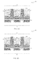
- FIG. 3 is a block diagram of a cross-sectional view depicting exemplary 3D IC packaged component 100 with via structures.
- 3D IC packaged component 100 includes multiple dies, such as for a system-in-a-package (“SiP”) or an interposer, namely generally for one or more dies used for or in D2D, W2D, or WLP interconnections for forming a 3D IC.
- SiP system-in-a-package
- interposer namely generally for one or more dies used for or in D2D, W2D, or WLP interconnections for forming a 3D IC.
- the particular configuration illustratively depicted in this example in FIG. 3 may, though need not, be used.
- This example is provided for purposes of clarity by way of example and not limitation, as it shall become apparent that a more or less complex configuration may be used.
- a first die and a second die interconnected to one another through die-to-die interconnects there is at least a first die and a second die interconnected to one another through die-to-die interconnects.
- IC dies 10 - 1 through 10 - 3 , as well as substrate 40 may each have thermal via structures (“thermal vias”) 118 for conducting heat in a generally vertical direction in 3D IC packaged component 100 .
- thermal vias thermal via structures
- heat may be conducted from one die to another die in a 3D stacked IC, and such heat may be provided to a heat sink, such as for example to thermal paste 42 and then to heat sink or heat spreader 43 .
- heat sink 43 is part of 3D IC packaged component 100 ; however, in another configuration, an external heat sink may be coupled to heat sink 43 .
- a 3D stacked IC may be encapsulated, and in such configuration thermal paste 42 may be provided to an outer surface of such encapsulation for thermal conduction and adhesion of an external heat sink.
- Via structures 118 are through die vias, as they extend between an upper and a lower surface of a die. Via structures 118 may include through substrate vias, as described below in additional detail.
- FIGS. 4A through 4G are schematic diagrams of cross-sectional views depicting an exemplary portion of a successively processed in-process IC die 400 .
- IC die 400 may be for a 3D stacked IC.
- openings 411 each have one or more sidewalls and a bottom surface or area generally depending upon a resulting geometric or other volumetric shape of such openings.
- openings 411 are generally cylindrical with a sidewall surface 421 and a base surface 422 ; however, other volumetric shapes may be used in other implementations.
- Base surface 422 is substantially below upper surface 14 and is proximate to a lower surface 16 .
- an offset region 423 of material of substrate 12 may be located between base surface 422 and lower surface 16 .
- a liner layer or liner 15 is deposited onto substrate 12 .
- liner 15 is deposited onto upper surface 14 , as well as on base surface 422 and along sidewall surface 421 of each of openings 411 .
- a conformal deposition of liner 15 is illustratively depicted in this example, in other implementations a less conformal deposition may be used.
- etch 432 to remove a portion of liner 15 exposed by patterned masking layer 431 may be performed.
- liner 15 is a silicon-dioxide (SiO 2 ) removable by an oxide etch, such as a buffered oxide etch (“BOE”) or buffered hydrofluoric acid (“BHF” or HF”) etch for example; however, other materials for liner 15 and/or other types of etches may be used in other examples.
- Other examples of liner 15 material may include a silicon oxide, a silicon nitride, or another dielectric material may be used to electrically isolate via structures 18 from substrate 12 .
- Liner 15 may have a thermal conductivity value equal to or less than approximately 3 W/(m K). However, for a thermal via structure, electrical isolation from a liner 15 may be omitted as a thermal via structure is generally not used for electrical conduction.
- a barrier layer 24 is deposited on liner 15 and onto surfaces 421 and 422 of opening 411 T.
- Barrier layer 24 may provide sufficient protection against diffusion of a thermally conductive material, as described below in additional detail, into substrate 12 .
- a conformal deposition of barrier layer 24 is illustratively depicted in this example, in other implementations a less conformal deposition may be used.
- signal via openings 411 S may have therein a stack of a liner 15 and a barrier layer 24
- thermal via opening 411 T may have just a barrier layer 24 therein.
- a conductor layer 441 for via conductors 21 may be deposited onto barrier layer 24 .
- Via conductor 21 may be as previously described herein, and such via conductor layer 441 may fill openings 411 S and 411 T, as well as be deposited on an upper surface of barrier layer 24 . It is not necessary that the conductive layer 441 completely fill openings 411 S and 411 T, as voids may be allowed for example.
- a via conductor 21 may generally consist of copper or a copper alloy.
- a via conductor 21 may additionally or alternatively include one or more other conductive materials such as tantalum, nickel, titanium, molybdenum, tungsten, aluminum, gold, silver, or solder, including various alloys or compounds of one or more of the these materials, and the like.
- a via conductor 21 may include non-metallic additives to control various environmental or operational parameters of a via structure.
- FIGS. 5A and 5B are schematic diagrams of cross-sectional views depicting an exemplary portion of the successively processed in-process IC die 400 of FIG. 4G .
- a thermal via structure need not be electrically conductive in comparison to a signal via structure. Because thermal via structures do not have to be formed of the same material or materials of signal via structures, rather than deposition of a conductive layer 441 as described with reference to FIG. 4G , a masking layer 501 may be deposited and patterned prior to such deposition of conductive layer 441 . In this example, such masking layer 501 is deposited and patterned to fill opening 411 T, and thus deposition of a conductive layer 441 may fill openings 411 S without filling already filled opening 411 T. In another implementation, masking layer 501 may be deposited and patterned to fill openings 411 S for deposition of a conductive layer 441 to fill opening 411 T.
- Such masking layer 501 may then be removed, and following such removal a conductive layer 502 may be deposited to fill opening 411 T.
- a thermally conductive material disposed in a thermal via structure is not a diffusion or migration risk with respect to contamination of substrate 12 , then barrier layer 24 in such thermal via structure may be omitted.
- both thermal and signal via structures have a common via conductor 21 material, and thus it shall be assumed that the configuration of FIG. 4G is used in the following description. However, it shall be apparent that the following description applies equally to the configuration of FIGS. 5A and 5B .
- FIG. 6A is a schematic diagram of a cross-sectional view depicting an exemplary portion of in-process IC die 400 of FIG. 4G after a CMP operation 601 .
- CMP operation 601 may be used to remove conductive material of conductive layer 441 and barrier material of barrier layer 24 generally disposed above an upper surface 610 of liner 15 , as illustratively depicted. Accordingly, via structures 611 corresponding to openings 411 may remain after CMP operation 601 .
- signal via structures 611 S may correspond to signal via openings 411 S
- thermal via structures such as thermal via structure 611 T for example, may correspond to thermal via openings, such as thermal via opening 411 T for example.
- Each thermal via structure 611 T may include a barrier layer 24 and a via conductor 21 , where such barrier layer 24 is positioned to at least substantially prevent diffusion or migration into substrate 12 of a material used to provide via conductor 21 .
- a barrier layer 24 may be disposed in at least one of a plurality of vias to provide a thermal via structure 611 T, where barrier layer 24 is disposed between a thermally conductive material of conductive layer 441 and substrate 12 .
- thermally conductive material it is generally meant a material, including without limitation a compound or other combination of two or more materials, having a thermal conductivity value equal to or greater than approximately 150 W/(mk) (i.e., higher than silicon for a silicon substrate).
- a thermal conductive material may include a metal.
- a metal may be selected from a group consisting of aluminum, copper, gold, silver, tungsten, and solder.
- thermally conductive material may include a carbon-based material.
- a carbon-based material may include graphene.
- thermally conductive material is copper.
- FIG. 6B is a schematic diagram of a cross-sectional view depicting an exemplary portion of in-process IC die 400 of FIG. 4G after a CMP operation 602 .
- CMP operation 602 may be used to remove conductive material of conductive layer 441 , barrier material of barrier layer 24 , and liner material of liner 15 generally disposed above an upper surface 14 of substrate 12 , as illustratively depicted.
- CMP operation 602 may be an extension of CMP operation 601 .
- via structures 611 corresponding to openings 411 may remain after CMP operation 602 .
- signal via structures 611 S may correspond to signal via openings 411 S
- thermal via structures, such as thermal via structure 611 T for example may correspond to thermal via openings, such as thermal via opening 411 T for example.
- Each thermal via structure 611 T may include a barrier layer 24 and a via conductor 21 , where such barrier layer 24 is positioned to at least substantially prevent diffusion or migration into substrate 12 of a material used to provide via conductor 21 .
- a barrier layer 24 may be disposed in at least one of a plurality of vias to provide a thermal via structure 611 T, where barrier layer 24 is disposed between a thermally conductive material of conductive layer 441 and substrate 12 .
- FIG. 6C is a schematic diagram of a top view depicting an exemplary portion of an in-process IC die 400 of FIG. 6B .
- Sets of via structures 611 S and 611 T may be formed in an array 661 .
- other shapes such as circles, ellipses, rectangles, polygons, or other shapes, may be used.
- the numbers of via structures 611 S and 611 T may be fewer or more than those illustratively depicted.
- channels such as generally indicated by dashed lines 671 and 672 , may be formed for via structures 611 S and 611 T.
- an array of channels may be formed for vias.
- structures other than or including channels may be used, such as concentric rings, zigzags, or other geometric forms.
- vias structures 611 S and 611 T may, though need not be, completely filled.
- vias 411 S and 411 T may be conformally plated leaving voids in via conductors 21 of vias structures 611 S and/or 611 T.
- a substrate 12 may have formed therein vias, where a subset of the vias do not having a liner layer located therein.
- a thermally conductive material may be deposited in all of the vias to provide signal and thermal via structures.
- Layers associated with BEOL operations are generally depicted as block 701 for purposes of clarity and not limitation.
- In-process IC die 400 is illustratively depicted as inverted for this backside reveal.
- CMP operation 700 may be used to remove a portion of substrate 12 , namely offset region 423 of material of substrate 12 , as well as lower portions (illustratively depicted as upper portions) of liner 15 and barrier layer 24 to expose lower surfaces 703 of each of via conductors 21 . With this removal, a lower portion 702 of via conductor 21 may be removed from thermal via structure 611 T, due to the absence of a liner layer 15 in a thermal via opening 411 T. Subsequent die-level or wafer-level processing may follow.
- a wafer may be for one or more dies of a system-in-a-package (“SiP”) or an interposer, namely generally for one or more dies used for or in D2D, W2D, or WLP interconnections for forming a 3D IC using IC die 400 .
- SiP system-in-a-package
- interposer namely generally for one or more dies used for or in D2D, W2D, or WLP interconnections for forming a 3D IC using IC die 400 .
- thermal conductivity is approximately 0.7 and 1.3 W/(mK), respectively. Avoidance of such liner 15 from a thermal via structure may thus improve thermal conductivity by removing such thermally insulating material, but also in effect such removed material may be replaced at least partially with a thermally conductive material to further enhance thermal conductivity of a thermal via structure. Additionally, to the extent that by volume barrier layer 24 in a thermal via structure is increased, such barrier layer 24 material has a higher thermal conductivity than a liner 15 material. For example, Ta, Ti, TiN, TaN, and ZrN respectively have thermal conductivities of approximately 57.5, 21.9, 19.2, 8.8, and 7 W/(mK).
- FIG. 8 is a schematic diagram of a cross-sectional view of a portion of an IC die 400 of FIG. 7B .
- a substrate 12 -to-liner 15 interface 804 there is a substrate 12 -to-liner 15 interface 804 , a liner 15 -to-barrier layer 24 interface 803 , and a barrier layer 24 -to-via conductor 21 interface 801 .
- a substrate 12 -to-barrier layer 24 interface 802 there is a substrate 12 -to-barrier layer 24 interface 802 , as well as a barrier layer 24 -to-via conductor 21 interface 801 .
- These interfaces 801 through 804 may have thermal resistances in addition to thermal resistances of the materials associated therewith. However, for a highly thermally conductive via conductor 21 , thermal resistance thereof may be small enough in comparison to these other thermal resistances to be excluded from a thermal resistance determination.
- thermal resistance of a signal via structure 611 S may be approximated as a sum of thermal resistances of interface 801 , barrier layer 24 , interface 803 , liner 15 , interface 804 , and substrate 12 .
- thermal resistance of a thermal via structure 611 T may be approximated as a sum of thermal resistances of interface 801 , barrier layer 24 , interface 802 , and substrate 12 . Accordingly, thermal resistance of a thermal via structure 611 T may be substantially less than thermal resistance of a signal via structure 611 S.
- a thermal via structure 611 T may form a portion of a through die thermal via 118 of FIG. 3 of an IC die 400 .
- thermal resistance R may be expressed in terms of distance, L, divided by thermal conductivity k
- each thermal resistance in the above equation may be replaced by a ratio L/k.
- L/k is particular to the thickness of a layer and the thermal conductivity of the material having such thickness.
- FIG. 9 is a graph depicting an exemplary function 900 in accordance with the above-described change in thermal resistivity over thermal resistivity ratio.
- Function 900 relates to percentage of reduction in thermal resistance, namely y-axis 902 , relative to distance from a thermal via structure, namely x-axis 901 .
Landscapes
- Chemical & Material Sciences (AREA)
- Chemical Kinetics & Catalysis (AREA)
- General Chemical & Material Sciences (AREA)
- Internal Circuitry In Semiconductor Integrated Circuit Devices (AREA)
- Engineering & Computer Science (AREA)
- Materials Engineering (AREA)
Abstract
Description
ΔR/R=R l/(R b +R l +R s).
Because thermal resistance R may be expressed in terms of distance, L, divided by thermal conductivity k, each thermal resistance in the above equation may be replaced by a ratio L/k. Each L/k is particular to the thickness of a layer and the thermal conductivity of the material having such thickness.
Along the above lines,
Claims (20)
Priority Applications (1)
| Application Number | Priority Date | Filing Date | Title |
|---|---|---|---|
| US15/066,983 US9818668B2 (en) | 2014-03-07 | 2016-03-10 | Thermal vias disposed in a substrate without a liner layer |
Applications Claiming Priority (2)
| Application Number | Priority Date | Filing Date | Title |
|---|---|---|---|
| US14/201,473 US9299572B2 (en) | 2014-03-07 | 2014-03-07 | Thermal vias disposed in a substrate without a liner layer |
| US15/066,983 US9818668B2 (en) | 2014-03-07 | 2016-03-10 | Thermal vias disposed in a substrate without a liner layer |
Related Parent Applications (1)
| Application Number | Title | Priority Date | Filing Date |
|---|---|---|---|
| US14/201,473 Division US9299572B2 (en) | 2014-03-07 | 2014-03-07 | Thermal vias disposed in a substrate without a liner layer |
Publications (2)
| Publication Number | Publication Date |
|---|---|
| US20160197026A1 US20160197026A1 (en) | 2016-07-07 |
| US9818668B2 true US9818668B2 (en) | 2017-11-14 |
Family
ID=52684748
Family Applications (2)
| Application Number | Title | Priority Date | Filing Date |
|---|---|---|---|
| US14/201,473 Active US9299572B2 (en) | 2014-03-07 | 2014-03-07 | Thermal vias disposed in a substrate without a liner layer |
| US15/066,983 Active US9818668B2 (en) | 2014-03-07 | 2016-03-10 | Thermal vias disposed in a substrate without a liner layer |
Family Applications Before (1)
| Application Number | Title | Priority Date | Filing Date |
|---|---|---|---|
| US14/201,473 Active US9299572B2 (en) | 2014-03-07 | 2014-03-07 | Thermal vias disposed in a substrate without a liner layer |
Country Status (3)
| Country | Link |
|---|---|
| US (2) | US9299572B2 (en) |
| KR (1) | KR102296721B1 (en) |
| WO (1) | WO2015134994A1 (en) |
Cited By (2)
| Publication number | Priority date | Publication date | Assignee | Title |
|---|---|---|---|---|
| US10770395B2 (en) | 2018-11-01 | 2020-09-08 | International Business Machines Corporation | Silicon carbide and silicon nitride interconnects |
| US20230317597A1 (en) * | 2019-05-24 | 2023-10-05 | Intel Corporation | Integrated circuit structures with contoured interconnects |
Families Citing this family (14)
| Publication number | Priority date | Publication date | Assignee | Title |
|---|---|---|---|---|
| US9299572B2 (en) | 2014-03-07 | 2016-03-29 | Invensas Corporation | Thermal vias disposed in a substrate without a liner layer |
| US9583417B2 (en) | 2014-03-12 | 2017-02-28 | Invensas Corporation | Via structure for signal equalization |
| JP2016029681A (en) * | 2014-07-25 | 2016-03-03 | イビデン株式会社 | Multilayer wiring board and manufacturing method thereof |
| US9368436B2 (en) * | 2014-08-04 | 2016-06-14 | Infineon Technologies Ag | Source down semiconductor devices and methods of formation thereof |
| JP6473595B2 (en) | 2014-10-10 | 2019-02-20 | イビデン株式会社 | Multilayer wiring board and manufacturing method thereof |
| US9583462B2 (en) * | 2015-01-22 | 2017-02-28 | Qualcomm Incorporated | Damascene re-distribution layer (RDL) in fan out split die application |
| US10383225B1 (en) * | 2018-08-10 | 2019-08-13 | Seagate Technology Llc | Interposer with offset-stacked traces |
| KR102801539B1 (en) * | 2019-06-14 | 2025-05-02 | 삼성전자주식회사 | Method of forming a semiconductor device using a thermally-decomposable layer, a semiconductor fabrication apparatus and the semiconductor device |
| US11715895B2 (en) | 2020-07-09 | 2023-08-01 | Seagate Technology Llc | Methods for making electrical connectors with an electrical interposer |
| US11276764B1 (en) * | 2020-08-09 | 2022-03-15 | Global Communication Semiconductors, Llc | Method of making high frequency InGaP/GaAs HBTs |
| US11955416B2 (en) * | 2021-09-15 | 2024-04-09 | Macronix International Co., Ltd. | Semiconductor structure and method for manufacturing the same |
| KR102768255B1 (en) | 2022-10-19 | 2025-02-17 | 충북대학교 산학협력단 | Bonding methods using vertical wire structure |
| KR102732872B1 (en) | 2022-10-19 | 2024-11-25 | 충북대학교 산학협력단 | Bonding materials using vertical wire structure and manufacturing thereof |
| TWI907135B (en) * | 2024-10-30 | 2025-12-01 | 聯華電子股份有限公司 | Semiconductor with tsv and fabricating method of the same |
Citations (15)
| Publication number | Priority date | Publication date | Assignee | Title |
|---|---|---|---|---|
| US6222276B1 (en) | 1998-04-07 | 2001-04-24 | International Business Machines Corporation | Through-chip conductors for low inductance chip-to-chip integration and off-chip connections |
| US7834461B2 (en) | 2006-09-27 | 2010-11-16 | Nec Electronics Corporation | Semiconductor apparatus |
| US8193039B2 (en) | 2010-09-24 | 2012-06-05 | Advanced Micro Devices, Inc. | Semiconductor chip with reinforcing through-silicon-vias |
| US20120261805A1 (en) | 2011-04-14 | 2012-10-18 | Georgia Tech Research Corporation | Through package via structures in panel-based silicon substrates and methods of making the same |
| US8294240B2 (en) | 2009-06-08 | 2012-10-23 | Qualcomm Incorporated | Through silicon via with embedded decoupling capacitor |
| WO2013118618A1 (en) | 2012-02-08 | 2013-08-15 | ソニー株式会社 | High frequency semiconductor device and fabrication method for same |
| US20130270711A1 (en) * | 2012-04-12 | 2013-10-17 | The Research Foundation Of State University Of New York | Apparatus and method for integration of through substrate vias |
| US8609506B2 (en) | 2009-01-26 | 2013-12-17 | Taiwan Semiconductor Manufacturing Company, Ltd. | On-chip heat spreader |
| US20130342231A1 (en) | 2012-06-21 | 2013-12-26 | Michael Alfano | Semiconductor substrate with onboard test structure |
| US8791575B2 (en) | 2010-07-23 | 2014-07-29 | Tessera, Inc. | Microelectronic elements having metallic pads overlying vias |
| US8796135B2 (en) | 2010-07-23 | 2014-08-05 | Tessera, Inc. | Microelectronic elements with rear contacts connected with via first or via middle structures |
| US8816505B2 (en) | 2011-07-29 | 2014-08-26 | Tessera, Inc. | Low stress vias |
| US8872345B2 (en) | 2011-07-07 | 2014-10-28 | Taiwan Semiconductor Manufacturing Company, Ltd. | Forming grounded through-silicon vias in a semiconductor substrate |
| US20150255364A1 (en) | 2014-03-07 | 2015-09-10 | Invensas Corporation | Thermal Vias Disposed in a Substrate Without a Liner Layer |
| US9257322B2 (en) | 2012-07-04 | 2016-02-09 | Industrial Technology Research Institute | Method for manufacturing through substrate via (TSV), structure and control method of TSV capacitance |
Family Cites Families (1)
| Publication number | Priority date | Publication date | Assignee | Title |
|---|---|---|---|---|
| US7303005B2 (en) | 2005-11-04 | 2007-12-04 | Graftech International Holdings Inc. | Heat spreaders with vias |
-
2014
- 2014-03-07 US US14/201,473 patent/US9299572B2/en active Active
-
2015
- 2015-03-09 KR KR1020167027837A patent/KR102296721B1/en active Active
- 2015-03-09 WO PCT/US2015/019520 patent/WO2015134994A1/en not_active Ceased
-
2016
- 2016-03-10 US US15/066,983 patent/US9818668B2/en active Active
Patent Citations (16)
| Publication number | Priority date | Publication date | Assignee | Title |
|---|---|---|---|---|
| US6222276B1 (en) | 1998-04-07 | 2001-04-24 | International Business Machines Corporation | Through-chip conductors for low inductance chip-to-chip integration and off-chip connections |
| US7834461B2 (en) | 2006-09-27 | 2010-11-16 | Nec Electronics Corporation | Semiconductor apparatus |
| US8609506B2 (en) | 2009-01-26 | 2013-12-17 | Taiwan Semiconductor Manufacturing Company, Ltd. | On-chip heat spreader |
| US8294240B2 (en) | 2009-06-08 | 2012-10-23 | Qualcomm Incorporated | Through silicon via with embedded decoupling capacitor |
| US8791575B2 (en) | 2010-07-23 | 2014-07-29 | Tessera, Inc. | Microelectronic elements having metallic pads overlying vias |
| US8796135B2 (en) | 2010-07-23 | 2014-08-05 | Tessera, Inc. | Microelectronic elements with rear contacts connected with via first or via middle structures |
| US8193039B2 (en) | 2010-09-24 | 2012-06-05 | Advanced Micro Devices, Inc. | Semiconductor chip with reinforcing through-silicon-vias |
| US20120261805A1 (en) | 2011-04-14 | 2012-10-18 | Georgia Tech Research Corporation | Through package via structures in panel-based silicon substrates and methods of making the same |
| US8872345B2 (en) | 2011-07-07 | 2014-10-28 | Taiwan Semiconductor Manufacturing Company, Ltd. | Forming grounded through-silicon vias in a semiconductor substrate |
| US8816505B2 (en) | 2011-07-29 | 2014-08-26 | Tessera, Inc. | Low stress vias |
| WO2013118618A1 (en) | 2012-02-08 | 2013-08-15 | ソニー株式会社 | High frequency semiconductor device and fabrication method for same |
| US20130270711A1 (en) * | 2012-04-12 | 2013-10-17 | The Research Foundation Of State University Of New York | Apparatus and method for integration of through substrate vias |
| US8969200B2 (en) | 2012-04-12 | 2015-03-03 | The Research Foundation Of State University Of New York | Apparatus and method for integration of through substrate vias |
| US20130342231A1 (en) | 2012-06-21 | 2013-12-26 | Michael Alfano | Semiconductor substrate with onboard test structure |
| US9257322B2 (en) | 2012-07-04 | 2016-02-09 | Industrial Technology Research Institute | Method for manufacturing through substrate via (TSV), structure and control method of TSV capacitance |
| US20150255364A1 (en) | 2014-03-07 | 2015-09-10 | Invensas Corporation | Thermal Vias Disposed in a Substrate Without a Liner Layer |
Non-Patent Citations (1)
| Title |
|---|
| International Search Report and Written Opinion for PCT/US2015/019520, dated Jul. 17, 2015. |
Cited By (2)
| Publication number | Priority date | Publication date | Assignee | Title |
|---|---|---|---|---|
| US10770395B2 (en) | 2018-11-01 | 2020-09-08 | International Business Machines Corporation | Silicon carbide and silicon nitride interconnects |
| US20230317597A1 (en) * | 2019-05-24 | 2023-10-05 | Intel Corporation | Integrated circuit structures with contoured interconnects |
Also Published As
| Publication number | Publication date |
|---|---|
| KR20160130839A (en) | 2016-11-14 |
| KR102296721B1 (en) | 2021-08-31 |
| US20150255364A1 (en) | 2015-09-10 |
| US9299572B2 (en) | 2016-03-29 |
| US20160197026A1 (en) | 2016-07-07 |
| WO2015134994A1 (en) | 2015-09-11 |
Similar Documents
| Publication | Publication Date | Title |
|---|---|---|
| USRE49987E1 (en) | Multiple plated via arrays of different wire heights on a same substrate | |
| US9741696B2 (en) | Thermal vias disposed in a substrate proximate to a well thereof | |
| US10957661B2 (en) | Interconnections for a substrate associated with a backside reveal | |
| US9818668B2 (en) | Thermal vias disposed in a substrate without a liner layer | |
| US9991231B2 (en) | Stacked die integrated circuit | |
| US9852969B2 (en) | Die stacks with one or more bond via arrays of wire bond wires and with one or more arrays of bump interconnects | |
| US9263394B2 (en) | Multiple bond via arrays of different wire heights on a same substrate | |
| US20150371938A1 (en) | Back-end-of-line stack for a stacked device | |
| US9070676B2 (en) | Bowl-shaped solder structure |
Legal Events
| Date | Code | Title | Description |
|---|---|---|---|
| AS | Assignment |
Owner name: INVENSAS CORPORATION, CALIFORNIA Free format text: ASSIGNMENT OF ASSIGNORS INTEREST;ASSIGNOR:GAO, GUILIAN;REEL/FRAME:037950/0532 Effective date: 20140307 |
|
| AS | Assignment |
Owner name: ROYAL BANK OF CANADA, AS COLLATERAL AGENT, CANADA Free format text: SECURITY INTEREST;ASSIGNORS:INVENSAS CORPORATION;TESSERA, INC.;TESSERA ADVANCED TECHNOLOGIES, INC.;AND OTHERS;REEL/FRAME:040797/0001 Effective date: 20161201 |
|
| STCF | Information on status: patent grant |
Free format text: PATENTED CASE |
|
| AS | Assignment |
Owner name: BANK OF AMERICA, N.A., NORTH CAROLINA Free format text: SECURITY INTEREST;ASSIGNORS:ROVI SOLUTIONS CORPORATION;ROVI TECHNOLOGIES CORPORATION;ROVI GUIDES, INC.;AND OTHERS;REEL/FRAME:053468/0001 Effective date: 20200601 |
|
| AS | Assignment |
Owner name: DTS, INC., CALIFORNIA Free format text: RELEASE BY SECURED PARTY;ASSIGNOR:ROYAL BANK OF CANADA;REEL/FRAME:052920/0001 Effective date: 20200601 Owner name: FOTONATION CORPORATION (F/K/A DIGITALOPTICS CORPORATION AND F/K/A DIGITALOPTICS CORPORATION MEMS), CALIFORNIA Free format text: RELEASE BY SECURED PARTY;ASSIGNOR:ROYAL BANK OF CANADA;REEL/FRAME:052920/0001 Effective date: 20200601 Owner name: INVENSAS BONDING TECHNOLOGIES, INC. (F/K/A ZIPTRONIX, INC.), CALIFORNIA Free format text: RELEASE BY SECURED PARTY;ASSIGNOR:ROYAL BANK OF CANADA;REEL/FRAME:052920/0001 Effective date: 20200601 Owner name: TESSERA ADVANCED TECHNOLOGIES, INC, CALIFORNIA Free format text: RELEASE BY SECURED PARTY;ASSIGNOR:ROYAL BANK OF CANADA;REEL/FRAME:052920/0001 Effective date: 20200601 Owner name: INVENSAS CORPORATION, CALIFORNIA Free format text: RELEASE BY SECURED PARTY;ASSIGNOR:ROYAL BANK OF CANADA;REEL/FRAME:052920/0001 Effective date: 20200601 Owner name: PHORUS, INC., CALIFORNIA Free format text: RELEASE BY SECURED PARTY;ASSIGNOR:ROYAL BANK OF CANADA;REEL/FRAME:052920/0001 Effective date: 20200601 Owner name: DTS LLC, CALIFORNIA Free format text: RELEASE BY SECURED PARTY;ASSIGNOR:ROYAL BANK OF CANADA;REEL/FRAME:052920/0001 Effective date: 20200601 Owner name: TESSERA, INC., CALIFORNIA Free format text: RELEASE BY SECURED PARTY;ASSIGNOR:ROYAL BANK OF CANADA;REEL/FRAME:052920/0001 Effective date: 20200601 Owner name: IBIQUITY DIGITAL CORPORATION, MARYLAND Free format text: RELEASE BY SECURED PARTY;ASSIGNOR:ROYAL BANK OF CANADA;REEL/FRAME:052920/0001 Effective date: 20200601 |
|
| MAFP | Maintenance fee payment |
Free format text: PAYMENT OF MAINTENANCE FEE, 4TH YEAR, LARGE ENTITY (ORIGINAL EVENT CODE: M1551); ENTITY STATUS OF PATENT OWNER: LARGE ENTITY Year of fee payment: 4 |
|
| MAFP | Maintenance fee payment |
Free format text: PAYMENT OF MAINTENANCE FEE, 8TH YEAR, LARGE ENTITY (ORIGINAL EVENT CODE: M1552); ENTITY STATUS OF PATENT OWNER: LARGE ENTITY Year of fee payment: 8 |
|
| AS | Assignment |
Owner name: ADEIA SEMICONDUCTOR TECHNOLOGIES LLC, CALIFORNIA Free format text: CHANGE OF NAME;ASSIGNOR:INVENSAS LLC;REEL/FRAME:073508/0751 Effective date: 20220815 Owner name: INVENSAS LLC, CALIFORNIA Free format text: CHANGE OF NAME;ASSIGNOR:INVENSAS CORPORATION;REEL/FRAME:073508/0668 Effective date: 20211001 |