US9812446B2 - Electronic apparatus with pocket of low permittivity material to reduce electromagnetic interference - Google Patents
Electronic apparatus with pocket of low permittivity material to reduce electromagnetic interference Download PDFInfo
- Publication number
- US9812446B2 US9812446B2 US15/085,534 US201615085534A US9812446B2 US 9812446 B2 US9812446 B2 US 9812446B2 US 201615085534 A US201615085534 A US 201615085534A US 9812446 B2 US9812446 B2 US 9812446B2
- Authority
- US
- United States
- Prior art keywords
- substrate
- switch
- capacitance
- air pocket
- insulation
- Prior art date
- Legal status (The legal status is an assumption and is not a legal conclusion. Google has not performed a legal analysis and makes no representation as to the accuracy of the status listed.)
- Expired - Fee Related
Links
Images


Classifications
-
- H01L27/0711—
-
- H—ELECTRICITY
- H10—SEMICONDUCTOR DEVICES; ELECTRIC SOLID-STATE DEVICES NOT OTHERWISE PROVIDED FOR
- H10D—INORGANIC ELECTRIC SEMICONDUCTOR DEVICES
- H10D84/00—Integrated devices formed in or on semiconductor substrates that comprise only semiconducting layers, e.g. on Si wafers or on GaAs-on-Si wafers
- H10D84/40—Integrated devices formed in or on semiconductor substrates that comprise only semiconducting layers, e.g. on Si wafers or on GaAs-on-Si wafers characterised by the integration of at least one component covered by groups H10D12/00 or H10D30/00 with at least one component covered by groups H10D10/00 or H10D18/00, e.g. integration of IGFETs with BJTs
- H10D84/401—Combinations of FETs or IGBTs with BJTs
- H10D84/403—Combinations of FETs or IGBTs with BJTs and with one or more of diodes, resistors or capacitors
-
- H01L24/32—
-
- H01L24/48—
-
- H01L24/73—
-
- H01L27/0727—
-
- H—ELECTRICITY
- H10—SEMICONDUCTOR DEVICES; ELECTRIC SOLID-STATE DEVICES NOT OTHERWISE PROVIDED FOR
- H10D—INORGANIC ELECTRIC SEMICONDUCTOR DEVICES
- H10D84/00—Integrated devices formed in or on semiconductor substrates that comprise only semiconducting layers, e.g. on Si wafers or on GaAs-on-Si wafers
- H10D84/80—Integrated devices formed in or on semiconductor substrates that comprise only semiconducting layers, e.g. on Si wafers or on GaAs-on-Si wafers characterised by the integration of at least one component covered by groups H10D12/00 or H10D30/00, e.g. integration of IGFETs
- H10D84/811—Combinations of field-effect devices and one or more diodes, capacitors or resistors
-
- H—ELECTRICITY
- H10—SEMICONDUCTOR DEVICES; ELECTRIC SOLID-STATE DEVICES NOT OTHERWISE PROVIDED FOR
- H10W—GENERIC PACKAGES, INTERCONNECTIONS, CONNECTORS OR OTHER CONSTRUCTIONAL DETAILS OF DEVICES COVERED BY CLASS H10
- H10W44/00—Electrical arrangements for controlling or matching impedance
- H10W44/601—Capacitive arrangements
-
- H01L21/8228—
-
- H01L2224/32245—
-
- H01L2224/48091—
-
- H01L2224/48106—
-
- H01L2224/48225—
-
- H01L2224/73265—
-
- H01L23/49562—
-
- H01L23/49568—
-
- H01L23/49575—
-
- H01L23/49582—
-
- H01L23/49589—
-
- H01L25/072—
-
- H01L2924/05032—
-
- H01L2924/05432—
-
- H01L2924/1715—
-
- H01L2924/17747—
-
- H01L2924/19041—
-
- H01L2924/19102—
-
- H01L2924/30105—
-
- H—ELECTRICITY
- H10—SEMICONDUCTOR DEVICES; ELECTRIC SOLID-STATE DEVICES NOT OTHERWISE PROVIDED FOR
- H10D—INORGANIC ELECTRIC SEMICONDUCTOR DEVICES
- H10D84/00—Integrated devices formed in or on semiconductor substrates that comprise only semiconducting layers, e.g. on Si wafers or on GaAs-on-Si wafers
- H10D84/01—Manufacture or treatment
- H10D84/0112—Integrating together multiple components covered by H10D8/00, H10D10/00 or H10D18/00, e.g. integrating multiple BJTs
- H10D84/0119—Integrating together multiple components covered by H10D8/00, H10D10/00 or H10D18/00, e.g. integrating multiple BJTs the components including complementary BJTs
-
- H—ELECTRICITY
- H10—SEMICONDUCTOR DEVICES; ELECTRIC SOLID-STATE DEVICES NOT OTHERWISE PROVIDED FOR
- H10D—INORGANIC ELECTRIC SEMICONDUCTOR DEVICES
- H10D84/00—Integrated devices formed in or on semiconductor substrates that comprise only semiconducting layers, e.g. on Si wafers or on GaAs-on-Si wafers
- H10D84/01—Manufacture or treatment
- H10D84/02—Manufacture or treatment characterised by using material-based technologies
- H10D84/03—Manufacture or treatment characterised by using material-based technologies using Group IV technology, e.g. silicon technology or silicon-carbide [SiC] technology
- H10D84/038—Manufacture or treatment characterised by using material-based technologies using Group IV technology, e.g. silicon technology or silicon-carbide [SiC] technology using silicon technology, e.g. SiGe
-
- H—ELECTRICITY
- H10—SEMICONDUCTOR DEVICES; ELECTRIC SOLID-STATE DEVICES NOT OTHERWISE PROVIDED FOR
- H10W—GENERIC PACKAGES, INTERCONNECTIONS, CONNECTORS OR OTHER CONSTRUCTIONAL DETAILS OF DEVICES COVERED BY CLASS H10
- H10W40/00—Arrangements for thermal protection or thermal control
- H10W40/20—Arrangements for cooling
- H10W40/25—Arrangements for cooling characterised by their materials
- H10W40/255—Arrangements for cooling characterised by their materials having a laminate or multilayered structure, e.g. direct bond copper [DBC] ceramic substrates
-
- H—ELECTRICITY
- H10—SEMICONDUCTOR DEVICES; ELECTRIC SOLID-STATE DEVICES NOT OTHERWISE PROVIDED FOR
- H10W—GENERIC PACKAGES, INTERCONNECTIONS, CONNECTORS OR OTHER CONSTRUCTIONAL DETAILS OF DEVICES COVERED BY CLASS H10
- H10W70/00—Package substrates; Interposers; Redistribution layers [RDL]
- H10W70/40—Leadframes
- H10W70/456—Materials
- H10W70/457—Materials of metallic layers on leadframes
-
- H—ELECTRICITY
- H10—SEMICONDUCTOR DEVICES; ELECTRIC SOLID-STATE DEVICES NOT OTHERWISE PROVIDED FOR
- H10W—GENERIC PACKAGES, INTERCONNECTIONS, CONNECTORS OR OTHER CONSTRUCTIONAL DETAILS OF DEVICES COVERED BY CLASS H10
- H10W70/00—Package substrates; Interposers; Redistribution layers [RDL]
- H10W70/40—Leadframes
- H10W70/461—Leadframes specially adapted for cooling
-
- H—ELECTRICITY
- H10—SEMICONDUCTOR DEVICES; ELECTRIC SOLID-STATE DEVICES NOT OTHERWISE PROVIDED FOR
- H10W—GENERIC PACKAGES, INTERCONNECTIONS, CONNECTORS OR OTHER CONSTRUCTIONAL DETAILS OF DEVICES COVERED BY CLASS H10
- H10W70/00—Package substrates; Interposers; Redistribution layers [RDL]
- H10W70/40—Leadframes
- H10W70/475—Capacitors in combination with leadframes
-
- H—ELECTRICITY
- H10—SEMICONDUCTOR DEVICES; ELECTRIC SOLID-STATE DEVICES NOT OTHERWISE PROVIDED FOR
- H10W—GENERIC PACKAGES, INTERCONNECTIONS, CONNECTORS OR OTHER CONSTRUCTIONAL DETAILS OF DEVICES COVERED BY CLASS H10
- H10W70/00—Package substrates; Interposers; Redistribution layers [RDL]
- H10W70/40—Leadframes
- H10W70/481—Leadframes for devices being provided for in groups H10D8/00 - H10D48/00
-
- H—ELECTRICITY
- H10—SEMICONDUCTOR DEVICES; ELECTRIC SOLID-STATE DEVICES NOT OTHERWISE PROVIDED FOR
- H10W—GENERIC PACKAGES, INTERCONNECTIONS, CONNECTORS OR OTHER CONSTRUCTIONAL DETAILS OF DEVICES COVERED BY CLASS H10
- H10W72/00—Interconnections or connectors in packages
- H10W72/071—Connecting or disconnecting
- H10W72/073—Connecting or disconnecting of die-attach connectors
- H10W72/07331—Connecting techniques
- H10W72/07336—Soldering or alloying
-
- H—ELECTRICITY
- H10—SEMICONDUCTOR DEVICES; ELECTRIC SOLID-STATE DEVICES NOT OTHERWISE PROVIDED FOR
- H10W—GENERIC PACKAGES, INTERCONNECTIONS, CONNECTORS OR OTHER CONSTRUCTIONAL DETAILS OF DEVICES COVERED BY CLASS H10
- H10W72/00—Interconnections or connectors in packages
- H10W72/071—Connecting or disconnecting
- H10W72/075—Connecting or disconnecting of bond wires
-
- H—ELECTRICITY
- H10—SEMICONDUCTOR DEVICES; ELECTRIC SOLID-STATE DEVICES NOT OTHERWISE PROVIDED FOR
- H10W—GENERIC PACKAGES, INTERCONNECTIONS, CONNECTORS OR OTHER CONSTRUCTIONAL DETAILS OF DEVICES COVERED BY CLASS H10
- H10W72/00—Interconnections or connectors in packages
- H10W72/30—Die-attach connectors
- H10W72/351—Materials of die-attach connectors
- H10W72/352—Materials of die-attach connectors comprising metals or metalloids, e.g. solders
-
- H—ELECTRICITY
- H10—SEMICONDUCTOR DEVICES; ELECTRIC SOLID-STATE DEVICES NOT OTHERWISE PROVIDED FOR
- H10W—GENERIC PACKAGES, INTERCONNECTIONS, CONNECTORS OR OTHER CONSTRUCTIONAL DETAILS OF DEVICES COVERED BY CLASS H10
- H10W72/00—Interconnections or connectors in packages
- H10W72/851—Dispositions of multiple connectors or interconnections
- H10W72/874—On different surfaces
- H10W72/884—Die-attach connectors and bond wires
-
- H—ELECTRICITY
- H10—SEMICONDUCTOR DEVICES; ELECTRIC SOLID-STATE DEVICES NOT OTHERWISE PROVIDED FOR
- H10W—GENERIC PACKAGES, INTERCONNECTIONS, CONNECTORS OR OTHER CONSTRUCTIONAL DETAILS OF DEVICES COVERED BY CLASS H10
- H10W72/00—Interconnections or connectors in packages
- H10W72/90—Bond pads, in general
- H10W72/951—Materials of bond pads
- H10W72/952—Materials of bond pads comprising metals or metalloids, e.g. PbSn, Ag or Cu
-
- H—ELECTRICITY
- H10—SEMICONDUCTOR DEVICES; ELECTRIC SOLID-STATE DEVICES NOT OTHERWISE PROVIDED FOR
- H10W—GENERIC PACKAGES, INTERCONNECTIONS, CONNECTORS OR OTHER CONSTRUCTIONAL DETAILS OF DEVICES COVERED BY CLASS H10
- H10W90/00—Package configurations
-
- H—ELECTRICITY
- H10—SEMICONDUCTOR DEVICES; ELECTRIC SOLID-STATE DEVICES NOT OTHERWISE PROVIDED FOR
- H10W—GENERIC PACKAGES, INTERCONNECTIONS, CONNECTORS OR OTHER CONSTRUCTIONAL DETAILS OF DEVICES COVERED BY CLASS H10
- H10W90/00—Package configurations
- H10W90/701—Package configurations characterised by the relative positions of pads or connectors relative to package parts
- H10W90/731—Package configurations characterised by the relative positions of pads or connectors relative to package parts of die-attach connectors
- H10W90/734—Package configurations characterised by the relative positions of pads or connectors relative to package parts of die-attach connectors between a chip and a stacked insulating package substrate, interposer or RDL
-
- H—ELECTRICITY
- H10—SEMICONDUCTOR DEVICES; ELECTRIC SOLID-STATE DEVICES NOT OTHERWISE PROVIDED FOR
- H10W—GENERIC PACKAGES, INTERCONNECTIONS, CONNECTORS OR OTHER CONSTRUCTIONAL DETAILS OF DEVICES COVERED BY CLASS H10
- H10W90/00—Package configurations
- H10W90/701—Package configurations characterised by the relative positions of pads or connectors relative to package parts
- H10W90/751—Package configurations characterised by the relative positions of pads or connectors relative to package parts of bond wires
- H10W90/754—Package configurations characterised by the relative positions of pads or connectors relative to package parts of bond wires between a chip and a stacked insulating package substrate, interposer or RDL
-
- H—ELECTRICITY
- H10—SEMICONDUCTOR DEVICES; ELECTRIC SOLID-STATE DEVICES NOT OTHERWISE PROVIDED FOR
- H10W—GENERIC PACKAGES, INTERCONNECTIONS, CONNECTORS OR OTHER CONSTRUCTIONAL DETAILS OF DEVICES COVERED BY CLASS H10
- H10W90/00—Package configurations
- H10W90/811—Multiple chips on leadframes
Definitions
- This application relates generally to improvements in power electronics module. More particularly the present disclosure relates a direct bond copper modified to reduce the electromagnetic interference and noise.
- Power modules of power electronics may be utilized in electric vehicles (EV) and hybrid electric vehicles (HEV) as a charger (changing AC to DC), an inverter (changing DC to AC), and/or a converter (DC to DC).
- EV electric vehicles
- HEV hybrid electric vehicles
- the power modules such as the charger, converter, and inverter generate an electrical noise.
- the electric noise caused by parasitic capacitance in the power module is one of the major sources of noise.
- a parasitic capacitance associated with chips of the power modules may be a source of electrical noise.
- the electrical noise further propagates through the power module to other components.
- the electric noise generated by the chips may propagate through the power module, and may interfere with other electronic devices of the vehicle.
- the charger, the inverter, and the converter generate noise which may propagate and may interfere with other vehicle components, such as auxiliary electronics and/or an electric motor.
- conventional power modules may include one or more noise filters.
- the noise filters can be bulky and heavy, thereby increasing the weight and footprint of the power module.
- the noise filters may occupy a significant portion of the footprint of the power modules. As such, an improvement over current technology that will allow reducing or eliminating the need for large and bulky noise filters.
- an electronic apparatus including a first substrate having a first surface and a second surface, a first switch connected to a second switch and soldered in series on the first surface of the first substrate creating a connection to allow switching between the first switch and the second switch at high frequency, an insulation having a third surface attached to the second surface of the first substrate, and a second substrate having a pocket of low permittivity located between the first switch and the second switch on a fourth surface of the insulation, the fourth surface being opposite to the third surface where the first switch and the second switch are located.
- FIG. 1 is an exemplary circuit of power electronics according to the background art.
- FIG. 2 illustrates a cross-section of the exemplary circuit of power electronics according to the background art.
- FIG. 3A illustrates a first configuration of a direct bond copper of the power electronics according to certain embodiments of the present disclosure.
- FIG. 3B illustrates a second configuration of a direct bond copper of the power electronics according to certain embodiments of the present disclosure.
- FIG. 3C illustrates a variation of the first configuration with air pocket completely enclosed by the insulation and the second substrate according to certain embodiments of the present disclosure.
- FIG. 4 illustrates an equivalent capacitance generated due the presence of an air pocket according to an exemplary embodiment of the present disclosure.
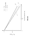
- FIG. 5A is a graph illustrating the effect of the air pocket on a capacitance of the power electronics according to an embodiment of the present disclosure.
- FIG. 5B is a graph illustrating the effect of increase in the air pocket area on a resulting capacitance of the power electronics according to an embodiment of the present disclosure.
- FIG. 6 is a graph illustrating the effect of air pocket on a noise level of the power electronics according to an embodiment of the present disclosure.
- FIG. 1 is an exemplary circuit of a power electronic device.
- the circuit 100 can include a power supply 101 , a first switch SW 1 and a second switch SW 2 .
- a positive (+) of the power supply 101 can be connected to a first drain 103 on the top surface of the first switch SW 1 .
- a negative ( ⁇ ) of the power supply 101 can be connected to a second source 107 of the second switch SW 2 .
- the first switch SW 1 and the second switch SW 2 can be connected in series by electrically connecting a first source 102 of the first switch SW 1 to a second drain 108 of the second switch SW 2 .
- the connection between the first switch SW 1 and the second switch SW 2 creates a high frequency point 105 during operation of the power electronics.
- the high frequency point 105 experiences a voltage change at a high frequency due to switching between the first switch SW 1 and the second switch SW 2 at a high frequency.
- the high frequency can range from kilohertz to gigahertz depending on the rated power of a system employing the power electronics.
- the high frequency point 105 can be a significant source of noise and electromagnetic interference in the circuit 100 which can transmit the noise and cause electromagnetic interference with other electric component of power electronics.
- An electrical connection between different elements of the circuit 100 creates several parasitic capacitances. For example, a first capacitance C 1 , a second capacitance C 2 , and a third capacitance C 3 are created in the circuit 100 .
- the first capacitance C 1 exist between the second source 107 of the second switch SW 2 and a substrate 120
- the second capacitance C 2 exist between the high frequency point 105 and the substrate 120
- the third capacitance C 3 exist between the first drain 103 and the substrate 120 .
- FIG. 2 illustrates a cross-section of the circuit 100 of the power electronic device.
- the power electronic device 100 can include a first substrate Cu 1 , a second substrate Cu 2 , and a third substrate Cu 3 attached on a first surface (above) an insulation 210 .
- a fourth substrate Cu 4 can be attached on a second surface (below) the insulation 210 .
- the fourth substrate Cu 4 can be soldered to a fifth substrate Cu 5 via a third solder 204 .
- the fifth substrate Cu 5 can dissipate the heat generated during operation of the power electronics.
- the substrates Cu 1 -Cu 5 can be electric conductors made of material such as copper, while the insulation 210 can be made of ceramic, aluminum oxide (Al 2 O 3 ), aluminum nitride (AlN), or the like.
- the first switch SW 1 and the second switch SW 2 can be soldered to the second substrate Cu 2 and the third substrate Cu 3 , respectively, on the first surface of the insulation 210 to create the circuit 100 .
- the switches SW 1 and SW 2 are soldered to different substrates.
- the substrates Cu 1 -Cu 3 can be configured differently to create the circuit 100 .
- the first switch SW 1 and the second switch SW 2 can be soldered to a single substrate such as the second substrate Cu 2 and the third substrate Cu 3 can be eliminated.
- the first switch SW 1 can be soldered to the third substrate Cu 3 via a first solder 201
- the second switch SW 2 can be soldered to the second substrate Cu 2 via a second solder 202 .
- first switch SW 1 and the second switch SW 2 can be electrically connected for example, in a series using bond wires.
- a first bond wire 211 creates a connection between the first switch SW 1 soldered on a third substrate Cu 3 and the second substrate Cu 2 , on which the second switch SW 2 is soldered.
- the second switch SW 2 can be connected to the first substrate Cu 1 by a second bond wire 213 to complete the circuit 100 .
- the first capacitance C 1 is created between the first substrate Cu 1 and the fourth substrate Cu 4 .
- the second capacitance C 2 is created between the second substrate Cu 2 and the fourth substrate Cu 4 .
- the third capacitance C 3 is created between the third substrate Cu 3 and the fourth substrate Cu 4 .
- the first, second, and third capacitances C 1 , C 2 , and C 3 respectively, include similar dielectric material i.e., the insulation 210 .
- the second capacitance C 2 is associated with the high frequency point 105 , as discussed earlier.
- FIG. 3A illustrates a direct bond copper 300 of the power electronics according to certain embodiments of the present disclosure.
- the direct bond copper 300 (DBC 300 hereinafter) refers to a part of the power electronics formed by the first switch SW 1 and the second SW 2 soldered to the second substrate Cu 2 on the first surface of the insulation 210 , while the second surface of the insulation 210 is attached to the fourth substrate Cu 4 .
- the DBC 300 includes a parasitic capacitance such as the second capacitance C 2 .
- a low permittivity material such as an air pocket 301 of a height H a and a width W a can be formed in the fourth substrate Cu 4 on the second surface of the insulation 210 , i.e., a surface opposite to the first surface, where the switches SW 1 and SW 2 are located.
- the low permittivity material can be any material having permittivity less than the surrounding substrate.
- the low permittivity material in solid, liquid or gaseous form. For instance, air (gaseous form) has a permittivity lower than the surrounding substrates Cu 2 , Cu 4 , solder, etc.
- the low permittivity material can be polyimides, SiO 2 , poly (aryl ethers), polynorbornene, polytetrafluoroethylene, or other polymers that are designed to have low permittivity as well as improved thermal and mechanical properties.
- the dimensions of the pocket of low permittivity material depend on the size of the circuit 100 .
- the volume of the air pocket is 3.82e-9 m3, and the ratio of air pocket area to the total DBC area is 16.5%.
- the air pocket 301 can be positioned in proximity of the high frequency point 105 (in FIG. 1 ), which corresponds to an area between the switches SW 1 and SW 2 in FIG. 3A .
- the air pocket 301 is positioned below the insulation 210 in the fourth substrate Cu 4 .
- the air pocket 301 can be further extended into the third solder 204 .
- the air pocket 301 is completely enclosed by the insulation 210 on one surface and the second substrate Cu 2 .
- the air pocket 301 can be extended into the fifth substrate Cu 5 , in which case the air pocket 301 will be completely enclosed by the insulation 210 on one surface and the fifth substrate Cu 4 .
- the air pocket 301 extends in a lateral direction (i.e., perpendicular to the plane of paper) along the length of the fourth substrates Cu 4 forming a channel.
- the air pocket 301 is not positioned directly beneath the first switch SW 1 and the second switch SW 2 .
- the air pocket 301 may be formed into an intermediate copper layer such as the fourth substrate Cu 4 and the solder 204 through an etching process.
- the air pocket 301 is rectangular in shape. It is understood that while a rectangular shape may be intended, the actual manufactured shape may have slight deviations in practice, for instance, rounded edges, jagged edges, etc.
- an air pocket of any other shape e.g., ring-like, circular, semicircular, triangular, etc.
- the DBC 300 having the air pocket 301 can be manufactured using traditional etching process used to fabricate integrated circuits.
- more than one pocket of low permittivity can be formed in the circuit, as illustrate in FIG. 3B .
- each of the more than one pockets of low permittivity can be filled with different permittivity material.
- FIG. 3B illustrates a second configuration of a direct bond copper of the power electronics according to certain embodiments of the present disclosure.
- the second configuration can include more than one pocket of low permittivity material, such as air pockets 301 and 302 .
- the air pockets 301 and 302 are in the vicinity of high frequency region of the circuit and in the path of noise propagation.
- the pocket of low permittivity material causes a change in capacitance of the circuit. For instance, the capacitance of a node N 1 can be evaluated, as illustrated in FIG. 4 .
- the node N 1 is a cross-section of the circuit having at least one pocket of low permittivity material such as air pocket 301 .
- FIG. 4 illustrates an equivalent capacitance of the node N 1 generated due the presence of the air pocket 301 according to an exemplary embodiment of the present disclosure.
- the node N 1 includes a part of the second substrate Cu 2 , a part of the fourth substrate Cu 4 having an area A 2 , the air pocket 301 having an area A air , and a fifth substrate Cu 5 .
- the node N 1 can have a total area A x .
- the total area A x can be a maximum area of the fifth substrate Cu 5 , or the area of the second substrate Cu 2 .
- the areas A 2 , A x and A air can be calculated in the x-y plane, as indicated in the FIG. 4 .
- the capacitances within the node N 1 include a capacitance C 21 between the second substrate Cu 2 and the fourth substrate Cu 4 separated by the insulator 210 , a capacitance C 22 between the second substrate Cu 2 and the air pocket 301 .
- the air pocket 301 can have a capacitance C a , which is formed in series with the capacitance C 22 .
- the resulting capacitance C 2 of a part of the power electronics device that includes the air pocket 301 can be defined by the equation 1 below,
- the capacitance C 21 is substantially equal to a product of the permittivity (i.e, ⁇ insulator ) Of the insulator 210 and the ratio of the area A 2 and thickness T of the insulator 210
- the capacitance C 22 is substantially equal to a product of the permittivity of the insulator 210 and the ratio of the area A air and thickness T of the insulator 210
- the capacitance C a which represents the capacitance across the low permittivity material such as the air pocket 301 , is substantially equal to a product of the permittivity of the low permittivity material (e.g. for air the permittivity is ⁇ air ) and the ratio of the area A air and height H a of the air pocket 301 .
- the resulting capacitance C′ 2 is a function of the area of the low permittivity material (i.e., the area of the air pocket 301 ), the area of different elements of the power electronics, as well as the thickness T of the insulation 210 and the height of the air pocket 301 .
- the second capacitance C 2 of a part of the power electronics device can be defined by the equation 2 below,
- the capacitance C a is lower than the capacitances C 1 , and C 2 .
- the resulting capacitance C′ 2 is lower than the second capacitance C 2 .
- the air pocket 301 reduces the capacitance of the power electronics, particularly beneath the first and second switches SW 1 and SW 2 , respectively.
- FIG. 5A is a graph illustrating the effect of the air pocket 301 on a capacitance of the power electronics according to an embodiment of the present disclosure.
- L 1 indicates a change in the resulting capacitance C′ 2 as a function of a change in the area of the DBC 300 , in which the thickness T of the insulation 210 is maintained at 1 mm and the air pocket 301 is not present.
- L 2 indicates a change in the equivalent capacitance C eq when the air pocket 301 is present in the DBC 300 .
- L 3 indicates a change in the resulting capacitance C′ 2 as a function of the change in the area of the DBC 300 , in which the thickness T of the insulation 210 is maintained at 0.3 mm and the air pocket 301 is not present. Comparing L 2 and L 3 shows that, when the air pocket 301 is present in the DBC 300 , the resulting capacitance C′ 2 reduces more sharply as the area (or volume) of the air pocket 301 increases relative to the area (or volume) of the DBC 300 . A similar effect is observed between L 2 and L 3 .
- FIG. 5B is a graph illustrating the effect of increase in the air pocket area on a resulting capacitance of the power electronics according to an embodiment of the present disclosure.
- the graph indicates that as the area A 2 decreases (as a result of increase in the air pocket's 301 area A air ), the resulting capacitance C′ 2 decreases rapidly compared to the second capacitance C 2 (i.e., capacitance when the air pocket 301 is not present).
- the power electronics with reduced capacitance i.e., the resulting capacitance C′ 2
- the resulting capacitance C′ 2 can decrease in a linear manner or non-linear manner depending on the type of low permittivity material and the dimensions of the air pocket.
- FIG. 6 is a graph illustrating the effect of the air pocket 301 on a noise level of the power electronics.
- the dotted line corresponds to a noise level observed as the frequency changes for a power electronics with the second capacitance C 2 (i.e., when the air pocket 301 is not present).
- the solid line corresponds to a noise level observed as the frequency changes for a power electronics with the resulting capacitance C′ 2 (i.e., when the air pocket 301 is present).
- the plots show that the peak noise reduces by a noise level NL 1 (e.g., 10 dB) when the air pocket 301 is present in the DBC 300 of the power electronics. Further, the plots show that the noise level over the entire frequency range of power electronics that includes the air pocket 301 is always lower than the noise level when an air pocket is not present.
- NL 1 e.g. 10 dB
Landscapes
- Shielding Devices Or Components To Electric Or Magnetic Fields (AREA)
- Engineering & Computer Science (AREA)
- Power Engineering (AREA)
- Structure Of Printed Boards (AREA)
Abstract
Description
Where, the capacitance C21 is substantially equal to a product of the permittivity (i.e, ∈insulator) Of the
Claims (9)
Priority Applications (1)
| Application Number | Priority Date | Filing Date | Title |
|---|---|---|---|
| US15/085,534 US9812446B2 (en) | 2016-03-30 | 2016-03-30 | Electronic apparatus with pocket of low permittivity material to reduce electromagnetic interference |
Applications Claiming Priority (1)
| Application Number | Priority Date | Filing Date | Title |
|---|---|---|---|
| US15/085,534 US9812446B2 (en) | 2016-03-30 | 2016-03-30 | Electronic apparatus with pocket of low permittivity material to reduce electromagnetic interference |
Publications (2)
| Publication Number | Publication Date |
|---|---|
| US20170287822A1 US20170287822A1 (en) | 2017-10-05 |
| US9812446B2 true US9812446B2 (en) | 2017-11-07 |
Family
ID=59961859
Family Applications (1)
| Application Number | Title | Priority Date | Filing Date |
|---|---|---|---|
| US15/085,534 Expired - Fee Related US9812446B2 (en) | 2016-03-30 | 2016-03-30 | Electronic apparatus with pocket of low permittivity material to reduce electromagnetic interference |
Country Status (1)
| Country | Link |
|---|---|
| US (1) | US9812446B2 (en) |
Cited By (1)
| Publication number | Priority date | Publication date | Assignee | Title |
|---|---|---|---|---|
| US11587856B2 (en) * | 2017-03-15 | 2023-02-21 | Abb Schweiz Ag | Solid state switching device |
Citations (13)
| Publication number | Priority date | Publication date | Assignee | Title |
|---|---|---|---|---|
| JPS6039374A (en) | 1983-08-12 | 1985-03-01 | Meidensha Electric Mfg Co Ltd | Output waveform improving method of inverter |
| JPS63177551A (en) | 1987-01-19 | 1988-07-21 | Hitachi Ltd | Solid-state imaging device and its manufacturing method |
| US5599413A (en) | 1992-11-25 | 1997-02-04 | Matsushita Electric Industrial Co., Ltd. | Method of producing a ceramic electronic device |
| US6219245B1 (en) | 2000-04-18 | 2001-04-17 | General Motors Corporation | Electrically isolated power switching device mounting assembly for EMI reduction |
| US6636429B2 (en) | 2000-09-20 | 2003-10-21 | Ballard Power Systems Corporation | EMI reduction in power modules through the use of integrated capacitors on the substrate level |
| US7038289B2 (en) | 2001-06-14 | 2006-05-02 | Stmicroelectronics Sa | Deep insulating trench |
| US20110241135A1 (en) | 2010-04-02 | 2011-10-06 | Kabushiki Kaisha Toshiba | Mems element |
| US8319278B1 (en) | 2009-03-31 | 2012-11-27 | Maxpower Semiconductor, Inc. | Power device structures and methods using empty space zones |
| US20140001488A1 (en) * | 2012-06-27 | 2014-01-02 | Luke Perkins | Electronic Device Including Silicon Carbide Diode Dies |
| US20140070304A1 (en) | 2012-09-11 | 2014-03-13 | Kabushiki Kaisha Toshiba | Nonvolatile memory device and method for manufacturing same |
| US8822269B2 (en) * | 2005-04-19 | 2014-09-02 | Renesas Electronics Corporation | Semiconductor device and method of manufacturing the same |
| US8932928B2 (en) * | 2012-05-14 | 2015-01-13 | Freescale Semiconductor, Inc. | Power MOSFET structure and method |
| US20150137378A1 (en) | 2013-11-15 | 2015-05-21 | Taiwan Semiconductor Manufacturing Company, Ltd. | Semiconductor Device having Voids and Method of Forming Same |
-
2016
- 2016-03-30 US US15/085,534 patent/US9812446B2/en not_active Expired - Fee Related
Patent Citations (13)
| Publication number | Priority date | Publication date | Assignee | Title |
|---|---|---|---|---|
| JPS6039374A (en) | 1983-08-12 | 1985-03-01 | Meidensha Electric Mfg Co Ltd | Output waveform improving method of inverter |
| JPS63177551A (en) | 1987-01-19 | 1988-07-21 | Hitachi Ltd | Solid-state imaging device and its manufacturing method |
| US5599413A (en) | 1992-11-25 | 1997-02-04 | Matsushita Electric Industrial Co., Ltd. | Method of producing a ceramic electronic device |
| US6219245B1 (en) | 2000-04-18 | 2001-04-17 | General Motors Corporation | Electrically isolated power switching device mounting assembly for EMI reduction |
| US6636429B2 (en) | 2000-09-20 | 2003-10-21 | Ballard Power Systems Corporation | EMI reduction in power modules through the use of integrated capacitors on the substrate level |
| US7038289B2 (en) | 2001-06-14 | 2006-05-02 | Stmicroelectronics Sa | Deep insulating trench |
| US8822269B2 (en) * | 2005-04-19 | 2014-09-02 | Renesas Electronics Corporation | Semiconductor device and method of manufacturing the same |
| US8319278B1 (en) | 2009-03-31 | 2012-11-27 | Maxpower Semiconductor, Inc. | Power device structures and methods using empty space zones |
| US20110241135A1 (en) | 2010-04-02 | 2011-10-06 | Kabushiki Kaisha Toshiba | Mems element |
| US8932928B2 (en) * | 2012-05-14 | 2015-01-13 | Freescale Semiconductor, Inc. | Power MOSFET structure and method |
| US20140001488A1 (en) * | 2012-06-27 | 2014-01-02 | Luke Perkins | Electronic Device Including Silicon Carbide Diode Dies |
| US20140070304A1 (en) | 2012-09-11 | 2014-03-13 | Kabushiki Kaisha Toshiba | Nonvolatile memory device and method for manufacturing same |
| US20150137378A1 (en) | 2013-11-15 | 2015-05-21 | Taiwan Semiconductor Manufacturing Company, Ltd. | Semiconductor Device having Voids and Method of Forming Same |
Non-Patent Citations (1)
| Title |
|---|
| Xun Gong, et al., "Investigation of Conducted EMI in SiC JFET Inverters Using Separated Heat Sinks", IEEE Transactions on Industrial Electronics, vol. 61, No. 1, Jan. 2014, pp. 115-125. |
Cited By (1)
| Publication number | Priority date | Publication date | Assignee | Title |
|---|---|---|---|---|
| US11587856B2 (en) * | 2017-03-15 | 2023-02-21 | Abb Schweiz Ag | Solid state switching device |
Also Published As
| Publication number | Publication date |
|---|---|
| US20170287822A1 (en) | 2017-10-05 |
Similar Documents
| Publication | Publication Date | Title |
|---|---|---|
| US20230171909A1 (en) | Semiconductor device with stacked terminals | |
| CN104471832B (en) | Wireless power transmission device, wireless power transmission device, and power receiving device | |
| US10068880B2 (en) | Power module | |
| JP5981519B2 (en) | Integrated capacitor and method of manufacturing the same | |
| US10637345B2 (en) | Semiconductor device and power conversion device | |
| US10888941B2 (en) | Power semiconductor module | |
| US10763346B2 (en) | Semiconductor device and power conversion apparatus | |
| US9610847B2 (en) | Power conversion device | |
| US10163811B2 (en) | Semiconductor package structure based on cascade circuits | |
| US9755544B2 (en) | Power conversion device | |
| US11495527B2 (en) | Semiconductor module | |
| JP6154104B2 (en) | Apparatus for electrically interconnecting at least one electronic component to a power supply including means for reducing loop inductance between the first and second terminals | |
| US10283475B2 (en) | Power module assembly with dual substrates and reduced inductance | |
| CN107393715B (en) | Capacitors, especially intermediate circuit capacitors for polyphase systems | |
| US9768100B1 (en) | Semiconductor device | |
| US9640474B1 (en) | Power semiconductor package having power semiconductor die in a support substrate with bar vias | |
| US10304770B2 (en) | Semiconductor device with stacked terminals | |
| US10734890B2 (en) | Power conversion device | |
| US9812446B2 (en) | Electronic apparatus with pocket of low permittivity material to reduce electromagnetic interference | |
| WO2020071098A1 (en) | Semiconductor module | |
| US20220263425A1 (en) | Electric circuit device | |
| US12532770B2 (en) | Switching device and switching module including a common mode current suppression structure | |
| US9190368B2 (en) | Semiconductor device that attenuates high-frequency oscillation | |
| CN110506384A (en) | Low inductance half-bridge power module | |
| US10638604B1 (en) | Insulated metal printed circuit board |
Legal Events
| Date | Code | Title | Description |
|---|---|---|---|
| AS | Assignment |
Owner name: TOYOTA MOTOR ENGINEERING & MANUFACTURING NORTH AME Free format text: ASSIGNMENT OF ASSIGNORS INTEREST;ASSIGNORS:SHIN, JONGWON;WANG, CHI-MING;SIGNING DATES FROM 20160318 TO 20160329;REEL/FRAME:038141/0652 |
|
| STCF | Information on status: patent grant |
Free format text: PATENTED CASE |
|
| AS | Assignment |
Owner name: TOYOTA JIDOSHA KABUSHIKI KAISHA, JAPAN Free format text: ASSIGNMENT OF ASSIGNORS INTEREST;ASSIGNOR:TOYOTA MOTOR ENGINEERING & MANUFACTURING NORTH AMERICA, INC.;REEL/FRAME:044341/0235 Effective date: 20171109 |
|
| AS | Assignment |
Owner name: DENSO CORPORATION, JAPAN Free format text: ASSIGNMENT OF ASSIGNORS INTEREST;ASSIGNOR:TOYOTA JIDOSHA KABUSHIKI KAISHA;REEL/FRAME:052281/0706 Effective date: 20191229 |
|
| MAFP | Maintenance fee payment |
Free format text: PAYMENT OF MAINTENANCE FEE, 4TH YEAR, LARGE ENTITY (ORIGINAL EVENT CODE: M1551); ENTITY STATUS OF PATENT OWNER: LARGE ENTITY Year of fee payment: 4 |
|
| FEPP | Fee payment procedure |
Free format text: MAINTENANCE FEE REMINDER MAILED (ORIGINAL EVENT CODE: REM.); ENTITY STATUS OF PATENT OWNER: LARGE ENTITY |
|
| LAPS | Lapse for failure to pay maintenance fees |
Free format text: PATENT EXPIRED FOR FAILURE TO PAY MAINTENANCE FEES (ORIGINAL EVENT CODE: EXP.); ENTITY STATUS OF PATENT OWNER: LARGE ENTITY |
|
| STCH | Information on status: patent discontinuation |
Free format text: PATENT EXPIRED DUE TO NONPAYMENT OF MAINTENANCE FEES UNDER 37 CFR 1.362 |
|
| FP | Lapsed due to failure to pay maintenance fee |
Effective date: 20251107 |