US9812370B2 - III-V, SiGe, or Ge base lateral bipolar transistor and CMOS hybrid technology - Google Patents

III-V, SiGe, or Ge base lateral bipolar transistor and CMOS hybrid technology Download PDF

Info

Publication number
US9812370B2
US9812370B2 US15/332,207 US201615332207A US9812370B2 US 9812370 B2 US9812370 B2 US 9812370B2 US 201615332207 A US201615332207 A US 201615332207A US 9812370 B2 US9812370 B2 US 9812370B2
Authority
US
United States
Prior art keywords
bipolar transistor
base
dummy gate
cmos fet
wafer
Prior art date
Legal status (The legal status is an assumption and is not a legal conclusion. Google has not performed a legal analysis and makes no representation as to the accuracy of the status listed.)
Active
Application number
US15/332,207
Other versions
US20170040219A1 (en
Inventor
Josephine B. Chang
Gen P. Lauer
Isaac Lauer
Jeffrey W. Sleight
Current Assignee (The listed assignees may be inaccurate. Google has not performed a legal analysis and makes no representation or warranty as to the accuracy of the list.)
Elpis Technologies Inc
Original Assignee
International Business Machines Corp
Priority date (The priority date is an assumption and is not a legal conclusion. Google has not performed a legal analysis and makes no representation as to the accuracy of the date listed.)
Filing date
Publication date
Application filed by International Business Machines Corp filed Critical International Business Machines Corp
Priority to US15/332,207 priority Critical patent/US9812370B2/en
Assigned to INTERNATIONAL BUSINESS MACHINES CORPORATION reassignment INTERNATIONAL BUSINESS MACHINES CORPORATION ASSIGNMENT OF ASSIGNORS INTEREST (SEE DOCUMENT FOR DETAILS). Assignors: LAUER, GEN P., LAUER, ISAAC, SLEIGHT, JEFFREY W., CHANG, JOSEPHINE B.
Publication of US20170040219A1 publication Critical patent/US20170040219A1/en
Application granted granted Critical
Publication of US9812370B2 publication Critical patent/US9812370B2/en
Assigned to ELPIS TECHNOLOGIES INC. reassignment ELPIS TECHNOLOGIES INC. ASSIGNMENT OF ASSIGNORS INTEREST (SEE DOCUMENT FOR DETAILS). Assignors: INTERNATIONAL BUSINESS MACHINES CORPORATION
Active legal-status Critical Current
Anticipated expiration legal-status Critical

Links

Images

Classifications

    • HELECTRICITY
    • H01ELECTRIC ELEMENTS
    • H01LSEMICONDUCTOR DEVICES NOT COVERED BY CLASS H10
    • H01L21/00Processes or apparatus adapted for the manufacture or treatment of semiconductor or solid state devices or of parts thereof
    • H01L21/70Manufacture or treatment of devices consisting of a plurality of solid state components formed in or on a common substrate or of parts thereof; Manufacture of integrated circuit devices or of parts thereof
    • H01L21/77Manufacture or treatment of devices consisting of a plurality of solid state components or integrated circuits formed in, or on, a common substrate
    • H01L21/78Manufacture or treatment of devices consisting of a plurality of solid state components or integrated circuits formed in, or on, a common substrate with subsequent division of the substrate into plural individual devices
    • H01L21/82Manufacture or treatment of devices consisting of a plurality of solid state components or integrated circuits formed in, or on, a common substrate with subsequent division of the substrate into plural individual devices to produce devices, e.g. integrated circuits, each consisting of a plurality of components
    • H01L21/822Manufacture or treatment of devices consisting of a plurality of solid state components or integrated circuits formed in, or on, a common substrate with subsequent division of the substrate into plural individual devices to produce devices, e.g. integrated circuits, each consisting of a plurality of components the substrate being a semiconductor, using silicon technology
    • H01L21/8248Combination of bipolar and field-effect technology
    • H01L21/8249Bipolar and MOS technology
    • HELECTRICITY
    • H01ELECTRIC ELEMENTS
    • H01LSEMICONDUCTOR DEVICES NOT COVERED BY CLASS H10
    • H01L21/00Processes or apparatus adapted for the manufacture or treatment of semiconductor or solid state devices or of parts thereof
    • H01L21/02Manufacture or treatment of semiconductor devices or of parts thereof
    • H01L21/04Manufacture or treatment of semiconductor devices or of parts thereof the devices having at least one potential-jump barrier or surface barrier, e.g. PN junction, depletion layer or carrier concentration layer
    • H01L21/18Manufacture or treatment of semiconductor devices or of parts thereof the devices having at least one potential-jump barrier or surface barrier, e.g. PN junction, depletion layer or carrier concentration layer the devices having semiconductor bodies comprising elements of Group IV of the Periodic System or AIIIBV compounds with or without impurities, e.g. doping materials
    • H01L21/24Alloying of impurity materials, e.g. doping materials, electrode materials, with a semiconductor body
    • H01L21/244Alloying of electrode materials
    • HELECTRICITY
    • H01ELECTRIC ELEMENTS
    • H01LSEMICONDUCTOR DEVICES NOT COVERED BY CLASS H10
    • H01L21/00Processes or apparatus adapted for the manufacture or treatment of semiconductor or solid state devices or of parts thereof
    • H01L21/70Manufacture or treatment of devices consisting of a plurality of solid state components formed in or on a common substrate or of parts thereof; Manufacture of integrated circuit devices or of parts thereof
    • H01L21/77Manufacture or treatment of devices consisting of a plurality of solid state components or integrated circuits formed in, or on, a common substrate
    • H01L21/78Manufacture or treatment of devices consisting of a plurality of solid state components or integrated circuits formed in, or on, a common substrate with subsequent division of the substrate into plural individual devices
    • H01L21/82Manufacture or treatment of devices consisting of a plurality of solid state components or integrated circuits formed in, or on, a common substrate with subsequent division of the substrate into plural individual devices to produce devices, e.g. integrated circuits, each consisting of a plurality of components
    • H01L21/84Manufacture or treatment of devices consisting of a plurality of solid state components or integrated circuits formed in, or on, a common substrate with subsequent division of the substrate into plural individual devices to produce devices, e.g. integrated circuits, each consisting of a plurality of components the substrate being other than a semiconductor body, e.g. being an insulating body
    • HELECTRICITY
    • H01ELECTRIC ELEMENTS
    • H01LSEMICONDUCTOR DEVICES NOT COVERED BY CLASS H10
    • H01L27/00Devices consisting of a plurality of semiconductor or other solid-state components formed in or on a common substrate
    • H01L27/02Devices consisting of a plurality of semiconductor or other solid-state components formed in or on a common substrate including semiconductor components specially adapted for rectifying, oscillating, amplifying or switching and having at least one potential-jump barrier or surface barrier; including integrated passive circuit elements with at least one potential-jump barrier or surface barrier
    • H01L27/04Devices consisting of a plurality of semiconductor or other solid-state components formed in or on a common substrate including semiconductor components specially adapted for rectifying, oscillating, amplifying or switching and having at least one potential-jump barrier or surface barrier; including integrated passive circuit elements with at least one potential-jump barrier or surface barrier the substrate being a semiconductor body
    • H01L27/06Devices consisting of a plurality of semiconductor or other solid-state components formed in or on a common substrate including semiconductor components specially adapted for rectifying, oscillating, amplifying or switching and having at least one potential-jump barrier or surface barrier; including integrated passive circuit elements with at least one potential-jump barrier or surface barrier the substrate being a semiconductor body including a plurality of individual components in a non-repetitive configuration
    • H01L27/0611Devices consisting of a plurality of semiconductor or other solid-state components formed in or on a common substrate including semiconductor components specially adapted for rectifying, oscillating, amplifying or switching and having at least one potential-jump barrier or surface barrier; including integrated passive circuit elements with at least one potential-jump barrier or surface barrier the substrate being a semiconductor body including a plurality of individual components in a non-repetitive configuration integrated circuits having a two-dimensional layout of components without a common active region
    • H01L27/0617Devices consisting of a plurality of semiconductor or other solid-state components formed in or on a common substrate including semiconductor components specially adapted for rectifying, oscillating, amplifying or switching and having at least one potential-jump barrier or surface barrier; including integrated passive circuit elements with at least one potential-jump barrier or surface barrier the substrate being a semiconductor body including a plurality of individual components in a non-repetitive configuration integrated circuits having a two-dimensional layout of components without a common active region comprising components of the field-effect type
    • H01L27/0623Devices consisting of a plurality of semiconductor or other solid-state components formed in or on a common substrate including semiconductor components specially adapted for rectifying, oscillating, amplifying or switching and having at least one potential-jump barrier or surface barrier; including integrated passive circuit elements with at least one potential-jump barrier or surface barrier the substrate being a semiconductor body including a plurality of individual components in a non-repetitive configuration integrated circuits having a two-dimensional layout of components without a common active region comprising components of the field-effect type in combination with bipolar transistors
    • HELECTRICITY
    • H01ELECTRIC ELEMENTS
    • H01LSEMICONDUCTOR DEVICES NOT COVERED BY CLASS H10
    • H01L29/00Semiconductor devices adapted for rectifying, amplifying, oscillating or switching, or capacitors or resistors with at least one potential-jump barrier or surface barrier, e.g. PN junction depletion layer or carrier concentration layer; Details of semiconductor bodies or of electrodes thereof  ; Multistep manufacturing processes therefor
    • H01L29/02Semiconductor bodies ; Multistep manufacturing processes therefor
    • H01L29/06Semiconductor bodies ; Multistep manufacturing processes therefor characterised by their shape; characterised by the shapes, relative sizes, or dispositions of the semiconductor regions ; characterised by the concentration or distribution of impurities within semiconductor regions
    • H01L29/10Semiconductor bodies ; Multistep manufacturing processes therefor characterised by their shape; characterised by the shapes, relative sizes, or dispositions of the semiconductor regions ; characterised by the concentration or distribution of impurities within semiconductor regions with semiconductor regions connected to an electrode not carrying current to be rectified, amplified or switched and such electrode being part of a semiconductor device which comprises three or more electrodes
    • H01L29/1004Base region of bipolar transistors
    • H01L29/1008Base region of bipolar transistors of lateral transistors
    • HELECTRICITY
    • H01ELECTRIC ELEMENTS
    • H01LSEMICONDUCTOR DEVICES NOT COVERED BY CLASS H10
    • H01L29/00Semiconductor devices adapted for rectifying, amplifying, oscillating or switching, or capacitors or resistors with at least one potential-jump barrier or surface barrier, e.g. PN junction depletion layer or carrier concentration layer; Details of semiconductor bodies or of electrodes thereof  ; Multistep manufacturing processes therefor
    • H01L29/40Electrodes ; Multistep manufacturing processes therefor
    • H01L29/43Electrodes ; Multistep manufacturing processes therefor characterised by the materials of which they are formed
    • H01L29/45Ohmic electrodes
    • H01L29/456Ohmic electrodes on silicon
    • HELECTRICITY
    • H01ELECTRIC ELEMENTS
    • H01LSEMICONDUCTOR DEVICES NOT COVERED BY CLASS H10
    • H01L29/00Semiconductor devices adapted for rectifying, amplifying, oscillating or switching, or capacitors or resistors with at least one potential-jump barrier or surface barrier, e.g. PN junction depletion layer or carrier concentration layer; Details of semiconductor bodies or of electrodes thereof  ; Multistep manufacturing processes therefor
    • H01L29/66Types of semiconductor device ; Multistep manufacturing processes therefor
    • H01L29/66007Multistep manufacturing processes
    • H01L29/66075Multistep manufacturing processes of devices having semiconductor bodies comprising group 14 or group 13/15 materials
    • H01L29/66227Multistep manufacturing processes of devices having semiconductor bodies comprising group 14 or group 13/15 materials the devices being controllable only by the electric current supplied or the electric potential applied, to an electrode which does not carry the current to be rectified, amplified or switched, e.g. three-terminal devices
    • H01L29/66234Bipolar junction transistors [BJT]
    • H01L29/6625Lateral transistors
    • HELECTRICITY
    • H01ELECTRIC ELEMENTS
    • H01LSEMICONDUCTOR DEVICES NOT COVERED BY CLASS H10
    • H01L29/00Semiconductor devices adapted for rectifying, amplifying, oscillating or switching, or capacitors or resistors with at least one potential-jump barrier or surface barrier, e.g. PN junction depletion layer or carrier concentration layer; Details of semiconductor bodies or of electrodes thereof  ; Multistep manufacturing processes therefor
    • H01L29/66Types of semiconductor device ; Multistep manufacturing processes therefor
    • H01L29/66007Multistep manufacturing processes
    • H01L29/66075Multistep manufacturing processes of devices having semiconductor bodies comprising group 14 or group 13/15 materials
    • H01L29/66227Multistep manufacturing processes of devices having semiconductor bodies comprising group 14 or group 13/15 materials the devices being controllable only by the electric current supplied or the electric potential applied, to an electrode which does not carry the current to be rectified, amplified or switched, e.g. three-terminal devices
    • H01L29/66409Unipolar field-effect transistors
    • H01L29/66477Unipolar field-effect transistors with an insulated gate, i.e. MISFET
    • H01L29/66545Unipolar field-effect transistors with an insulated gate, i.e. MISFET using a dummy, i.e. replacement gate in a process wherein at least a part of the final gate is self aligned to the dummy gate
    • HELECTRICITY
    • H01ELECTRIC ELEMENTS
    • H01LSEMICONDUCTOR DEVICES NOT COVERED BY CLASS H10
    • H01L29/00Semiconductor devices adapted for rectifying, amplifying, oscillating or switching, or capacitors or resistors with at least one potential-jump barrier or surface barrier, e.g. PN junction depletion layer or carrier concentration layer; Details of semiconductor bodies or of electrodes thereof  ; Multistep manufacturing processes therefor
    • H01L29/66Types of semiconductor device ; Multistep manufacturing processes therefor
    • H01L29/68Types of semiconductor device ; Multistep manufacturing processes therefor controllable by only the electric current supplied, or only the electric potential applied, to an electrode which does not carry the current to be rectified, amplified or switched
    • H01L29/70Bipolar devices
    • H01L29/72Transistor-type devices, i.e. able to continuously respond to applied control signals
    • H01L29/73Bipolar junction transistors
    • H01L29/735Lateral transistors

Definitions

  • the present invention relates to lateral bipolar transistor and CMOS hybrid technology and more particularly, to techniques for integrating a III-V, SiGe, or Ge base lateral bipolar transistor with CMOS technology.
  • Bipolar transistors are electronic devices with two P-N junctions that are in close proximity to one another.
  • a common bipolar transistor has three regions: i) an emitter, ii) a collector, and iii) a base present between the emitter and the collector. If the emitter and the collector are doped with an n-type dopant and the base is doped with a p-type dopant, then the device is an “NPN” transistor. Alternatively, if the emitter and the collector are doped with a p-type dopant and the base is doped with an n-type dopant, then the device is a “PNP” transistor.
  • bipolar transistors have superior device attributes in some areas, especially for analogue and power gain applications.
  • Conventional bipolar devices require abrupt emitter-to-base junctions and well controlled base region lengths and are typically not scaled for circuit density of CMOS structures.
  • bipolar transistor designs and techniques for fabrication thereof would be desirable, especially when compatible with CMOS FET fabrication processes.
  • the present invention provides techniques for integrating a III-V. SiGe, or Ge base lateral bipolar transistor with CMOS technology.
  • a method of fabricating a bipolar transistor device on a wafer includes the following steps.
  • a dummy gate is formed on the wafer, wherein the dummy gate is present over a portion of the wafer that serves as a base of the bipolar transistor.
  • the wafer is doped to form emitter and collector regions on both sides of the dummy gate.
  • a dielectric filler layer is deposited onto the wafer surrounding the dummy gate.
  • the dummy gate is removed selective to the dielectric filler layer, thereby exposing the base.
  • the base is recessed.
  • the base is re-grown from an epitaxial material selected from the group consisting of: SiGe, Ge, and a III-V material. Contacts are formed to the base.
  • a method of co-fabricating at least one CMOS FET device and at least one bipolar transistor device on a wafer includes the following steps. At least one CMOS FET dummy gate and at least one bipolar transistor dummy gate are formed on the wafer, wherein the CMOS FET dummy gate is present over a portion of the wafer that serves as a channel region of the CMOS FET device and the bipolar transistor dummy gate is present over a portion of the wafer that serves as a base of the bipolar transistor.
  • the wafer is doped to form emitter and collector regions on both sides of the bipolar transistor dummy gate.
  • the wafer is doped to form source and drain regions on both sides of the CMOS FET dummy gate.
  • a dielectric filler layer is deposited onto the wafer surrounding the CMOS FET dummy gate and the bipolar transistor dummy gate.
  • the CMOS FET dummy gate and the bipolar transistor dummy gate are removed selective to the dielectric filler layer, wherein removal of the CMOS FET dummy gate results in at least one first trench being formed in the dielectric filler layer and removal of the bipolar transistor dummy gate results in at least one second trench being formed in the dielectric filler layer.
  • the base of the bipolar transistor is recessed.
  • the base of the bipolar transistor is re-grown from an epitaxial material selected from the group consisting of: SiGe, Ge, and a III-V material.
  • a replacement gate of the CMOS FET device is formed in the first trench over the channel region of the CMOS FET device. Contacts are formed to the replacement gate of the CMOS FET device and to the base of the bipolar transistor device.
  • a bipolar transistor device in yet another aspect of the invention, includes emitter and collector regions formed in a wafer; and a base formed in the wafer between the emitter and collector regions, wherein a portion of the wafer in which the base is formed is recessed and contains an epitaxial material selected from the group consisting of: SiGe, Ge, and a III-V material.
  • FIG. 1 is a cross-sectional diagram illustrating a starting platform for an integrated CMOS FET and lateral bipolar transistor process flow, including a SOI wafer, CMOS FET and bipolar transistor dummy gates on the wafer, and spacers adjacent to the dummy gates according to an embodiment of the present invention;
  • FIG. 2 is a cross-sectional diagram illustrating doping having been used to form collector/emitter regions on both sides of the bipolar transistor dummy gate, while the CMOS FET is masked according to an embodiment of the present invention
  • FIG. 3 is a cross-sectional diagram illustrating doping having been used to form source/drain regions on both sides of the CMOS FET dummy gate, while the bipolar transistor is masked according to an embodiment of the present invention
  • FIG. 4 is a cross-sectional diagram illustrating a dielectric filler layer having been deposited onto the wafer, surrounding the dummy gates according to an embodiment of the present invention
  • FIG. 5 is a cross-sectional diagram illustrating the dummy gates having been removed from the CMOS FET and bipolar transistor devices according to an embodiment of the present invention
  • FIG. 6 is a cross-sectional diagram illustrating masking of the CMOS FET device(s) and the base in the bipolar transistor device(s) having been recessed according to an embodiment of the present invention
  • FIG. 7 is a cross-sectional diagram illustrating re-growth of the base in the bipolar transistor device(s) from an epitaxial SiGe, Ge or III-V semiconductor material according to an embodiment of the present invention
  • FIG. 8 is a cross-sectional diagram illustrating optional inner spacers having been formed in the bipolar transistor device(s) according to an embodiment of the present invention.
  • FIG. 9 is a cross-sectional diagram illustrating a replacement gate stack(s) having been formed over the CMOS FET device(s) while the bipolar transistor device(s) are masked according to an embodiment of the present invention
  • FIG. 10 is a cross-sectional diagram illustrating a layer of polysilicon having been blanket deposited onto the wafer, covering the CMOS FET device(s) and bipolar transistor devices according to an embodiment of the present invention
  • FIG. 11 is a cross-sectional diagram illustrating the polysilicon layer having been removed from over all but the gate electrode in the CMOS FET device(s) and the base of the bipolar transistor device(s) according to an embodiment of the present invention
  • FIG. 12 is a cross-sectional diagram illustrating a self-aligned silicide having been formed to produce gate electrode and base contacts in the CMOS FET and bipolar transistor devices according to an embodiment of the present invention
  • FIG. 13 is a cross-sectional diagram, following from FIG. 9 , which illustrates an alternative embodiment wherein the dielectric filler layer has been removed, and a self-aligned silicide having been used to form source/drain contacts and a gate electrode contact in the CMOS FET device(s), and emitter/collect contacts and a base contact in the bipolar transistor device(s) according to an embodiment of the present invention;
  • FIG. 14 is a cross-sectional diagram, following from FIG. 9 , which illustrates another alternative embodiment wherein epitaxy is used to thicken the base in the bipolar transistor device(s) according to an embodiment of the present invention.
  • FIG. 15 is a cross-sectional diagram, following from FIG. 14 , which illustrates the dielectric filler layer having been removed, and a self-aligned silicide having been used to form source/drain contacts and a gate electrode contact in the CMOS FET device(s), and emitter/collect contacts and a base contact in the bipolar transistor device(s) according to an embodiment of the present invention.
  • CMOS field-effect transistors FETs
  • bipolar transistors have silicon (Si)-based designs. See, for example, U.S. patent application Ser. No. 13/607,877, filed by J. Sleight et al., entitled “A Lateral Bipolar Transistor and CMOS Hybrid Technology,” the entire contents of which are incorporated by reference herein.
  • Si silicon
  • III-V materials can have significantly higher electron mobility than Si.
  • FIGS. 1-15 provide an exemplary methodology for co-fabricating a CMOS FET and a lateral bipolar transistor on a wafer.
  • the figures illustrate the formation of one CMOS FET and one lateral bipolar transistor.
  • multiple FETs and/or multiple bipolar transistors can be formed in the same manner as now described.
  • the present bipolar transistor fabrication techniques are shown integrated with a CMOS FET process flow, if so desired the present techniques may be implemented, in the same manner described herein, to fabricate a bipolar transistor device(s) alone, i.e., independent of other devices on the wafer.
  • the depiction of the fabrication of a CMOS FET(s) and a bipolar transistor(s) concurrently on a wafer is only an example intended to show how the present techniques are compatible with a FET fabrication process.
  • the starting platform for the process is a semiconductor wafer, such as a bulk semiconductor (e.g., silicon (Si), silicon germanium (SiGe), Ge, etc.) or semiconductor-on-insulator (SOD wafer.
  • a SOI wafer 101 is employed.
  • the SOI wafer 101 includes an SOI layer 102 separated from a substrate 106 by a buried oxide (or BOX) 104 .
  • the SOI layer 102 is formed from a semiconductor material including, but not limited to, Si, SiGe, Ge, and a III-V semiconductor material.
  • III-V semiconductor material or simply III-V material, as used herein and throughout the following description, refers to a material that includes at least one group III element and at least one group V element.
  • suitable III-V materials include, but are not limited to, one or more of aluminum gallium arsenide, aluminum gallium nitride, aluminum indium arsenide, aluminum nitride, gallium antimonide, gallium arsenide, gallium nitride, indium antimonide, indium arsenide, indium gallium arsenide, indium gallium nitride, indium phosphide and combinations including at least one of the foregoing materials.
  • the III-V material is indium gallium arsenide (InGaAs).
  • CMOS FET complementary metal-oxide-semiconductor
  • bipolar transistor the active regions of the wafer (i.e., in which the devices will be formed) are separated using standard isolation techniques, such as shallow trench isolation (STI).
  • STI shallow trench isolation
  • the present techniques utilize a replacement gate-based approach. Namely, as shown in FIG. 1 , at least one dummy gate 108 is formed on the wafer in the CMOS FET region and at least one dummy gate 110 is formed on the wafer in the bipolar transistor region. As shown in FIG. 1 , the dummy gates 108 and 110 are separated from the SOI layer 102 by a dummy gate dielectric.
  • the dummy gates are formed concurrently in the CMOS FET and bipolar transistor regions by first forming an interfacial oxide on the SOI layer 102 which will serve as the dummy gate dielectric.
  • This oxide e.g., silicon dioxide (SiO 2 )
  • SiO 2 silicon dioxide
  • the dummy gate oxide serves as an etch stop layer. Namely, during the dummy gate removal step (see below), the presence of an etch stop layer permits the dummy gate material to be removed selective to the underlying SOI.
  • a suitable dummy gate material e.g., poly-silicon
  • a suitable dummy gate material can then be blanket deposited onto the wafer, over the interfacial (dummy gate) oxide.
  • Standard lithography and etching processes can then be performed to pattern the dummy gate material and interfacial oxide with the footprints and locations of the dummy gates, thus forming dummy gate 108 (and dummy gate oxide) in the CMOS FET region and dummy gate 110 (and dummy gate oxide) in the bipolar transistor region.
  • the dummy gate 108 is present over a portion of the wafer that serves as a channel region of the CMOS FET device, and the dummy gate 110 is present over a portion of the wafer that serves as a base of the bipolar FET device.
  • spacers 112 and spacers 114 are then formed on opposite sides of the dummy gates 108 and 110 , respectively.
  • the spacers are formed concurrently in the CMOS FIT and bipolar transistor regions by first depositing a spacer material (e.g., a nitride material such as silicon nitride), and then patterning the material to form the spacers 112 / 114 .
  • a spacer material e.g., a nitride material such as silicon nitride
  • CMOS FET(s) are being fabricated on the same wafer (such as in the example of FIG. 2 ).
  • CMOS FETs e.g., using a resist or hardmask
  • Suitable hardmask materials include, but are not limited to, nitride materials such as silicon nitride (SiN). Standard lithography and etching techniques can be used to pattern the mask.
  • collector/emitter doping is then performed to form doped collector/emitter regions 202 (either N+ or P+) on both sides of the dummy gate 110 .
  • Conventional doping processes can be employed.
  • the doping can be also be achieved using solid source diffusion.
  • the dopant dose can be from about 5 ⁇ 10 18 atoms/cm 3 to about 5 ⁇ 10 20 atoms/cm 3 , e.g., from about 5 ⁇ 10 19 atoms/cm 3 to about 2 ⁇ 10 20 atoms/cm 3 .
  • NPN bipolar transistor configuration both sides of dummy the gate 110 can receive a number of successive implants of boron ions at various energies.
  • a PNP bipolar transistor configuration both sides of the dummy gate 110 can receive successive implantation steps of either arsenic or phosphoric ions.
  • the mask can be removed from the CMOS FET device(s).
  • the same general process can also be used dope source/drain regions 302 on both sides of the dummy gate 108 . See FIG. 3 .
  • a mask e.g., resist or hardmask
  • a conventional dopant implantation process can be used to form the source and drain regions 302 of the FET device(s).
  • the order in which the collector/emitter ( FIG. 2 ) and source/drain doping ( FIG. 3 ) is performed is immaterial and these processes can be performed in either order.
  • the mask can be removed from the bipolar transistor device(s).
  • a dielectric filler layer 402 is blanket deposited onto the wafer, surrounding the dummy gates. See FIG. 4 . As shown in FIG. 4 , the dielectric filler layer 402 is then planarized down to a top of the dummy gates. This will permit removal of the dummy gates later in the process. Planarization of the dielectric filler layer 402 can be performed using chemical mechanical polishing (CMP).
  • CMP chemical mechanical polishing
  • steps are provided first for forming an epitaxial material as the base of the bipolar transistor device(s) followed by replacement gate processing in the CMOS FET device(s). This sequence is presented only as an example. The steps described herein can be performed in any order, and in some cases steps can be performed concurrently with one another.
  • the dummy gates 108 and 110 are next removed from the CMOS FET and bipolar transistor devices.
  • the dummy gates 108 and 110 can be removed selective to the dielectric filler layer 402 and spacers 112 / 114 using wet chemical etching or dry etching. Removal of the dummy gates results in trenches being formed in the dielectric filler layer. In the case of the bipolar transistor device(s), removal of the dummy gate exposes the base.
  • CMOS FET device(s) are masked (e.g., with a resist or hardmask). See FIG. 6 .
  • the base in the bipolar transistor device(s) is/are recessed. See FIG. 6 .
  • This base recess can be performed using a selective etch, such as a selective reactive ion etching (RIE) process.
  • RIE reactive ion etching
  • the emitter and collector are covered/protected by the dielectric filler layer 402 and (as provided above) the CMOS FET device(s) are masked.
  • a RIE process for example, is anisotropic and if employed will result in portions of the (SOI) base below/masked by the spacers 114 to remain following the base recess etch. See FIG. 6 . Further, the etch should be endpointed prior to removing all of the (SOI) at the bottom of the base. These remaining portions of the SOI at the bottom and sides of the base will be used to template re-growth of the base using SiGe, Ge or a III-V semiconductor material.
  • the base is re-grown at this stage from an epitaxial SiGe, Ge or III-V semiconductor material 702 .
  • Re-growth of the base material permits the base to be formed from a different material than the collector and emitter regions (i.e., that of the SOI layer 102 ).
  • the material from which to re-grow the base is preferably chosen such that the bandgap in the base is smaller than the bandgap of the collector/emitter.
  • the collector/emitter regions are formed from doped portions of the SOI layer 102 .
  • the SOI layer can be formed from a semiconductor material, such as Si, SiGe, Ge, and a III-V semiconductor material.
  • the base is preferably re-grown from a material with a lower bandgap than the SOI layer.
  • Bandgap data for each of the above-described SOI and base materials may be found in the published literature. See, for instance, Helmut Foll, “Semiconductors 1, 5.1.4 Wavelength Engineering” Kiel University, Germany (accessed on Aug.
  • the base can be doped in-situ during this re-growth process.
  • Suitable dopants include, but are not limited to boron (p-type) and phosphorous (n-type).
  • a suitable base doping concentration is from about 1 ⁇ 10 17 cm 3 to about 1 ⁇ 10 18 cm 3 , e.g., from about 2 ⁇ 10 17 cm 3 to about 5 ⁇ 10 17 cm 3 . It is notable that doping the base at this stage is optional, and the base can be doped later in the process.
  • Defects in the depletion region act as carrier generation/recombination centers that reduce the gain of bipolar transistors. So, an anneal that moves the doping far enough that the defects are in a quasi-neutral region is advantageous.
  • the amount of diffusion depends on the width of the depletion region which depends on the doping concentration and the applied biases, as so:
  • the depletion region is preferably moved a distance of less than about 10 nanometers (nm) (e.g., from about 1 nm to about 8 nm) away from the re-growth interface.
  • nm nanometers
  • the base material is epitaxial Si or SiGe
  • the base including doped epitaxial SiGe, Ge or III-V (and associated out-diffusion region) or epitaxial SiGe, Ge or III-V doped later in the process using, e.g., solid-source diffusion (see below) will be given reference numeral 702 .
  • optional inner spacers 802 can be formed in the bipolar transistor device(s). Placing spacers 802 between what will be the collector/emitter regions of the device and the device contact will help to minimize parasitic capacitance in the completed device.
  • spacers 802 are formed by first depositing a nitride layer into the trench. A resist film is then deposited on the nitride layer, masked and patterned with the spacer footprints. A nitride-selective RIE is then used to define spacers in the nitride layer. The CMOS FET device(s) remain masked during this inner spacer formation process. The remainder of the steps of the process will be illustrated in the figures with the optional inner spacers present, however the same steps would be performed, in the same manner described, whether or not the inner spacers 802 are present.
  • processing of the CMOS FET device(s) is now conducted in order to form a replacement gate in the FET device(s).
  • any masking present over the CMOS FET device(s) is removed.
  • the dummy gate has already been removed selective to the dielectric filler layer and spacers. This step (illustrated in FIG. 5 ) was performed concurrently in both the CMOS FET and bipolar transistor devices. However, it is possible to leave the CMOS FET dummy gate(s) in place until this point when the replacement gate is formed. Regardless, removal of the dummy gate(s) in the CMOS FET device(s) results in a trench(es) being formed in the dielectric filler layer.
  • the replacement gate stack(s) include a gate dielectric 902 and a gate electrode 904 .
  • the gate dielectric separates the gate electrode from the portion of the SOI that will serve as a channel region of the CMOS FET device(s).
  • each FET will include a source region and a drain region interconnected by a channel region, and a gate electrode over the channel region that regulates electron flow through the channel.
  • the gate electrode can be formed from a metal or combination of metals and/or doped polysilicon.
  • a metal gate a high-k dielectric, such as hafnium oxide, is preferred.
  • a dummy gate dielectric was employed as an etch stop earlier in the process. Any of this dummy gate dielectric remaining is preferably removed and replaced with the gate dielectric 902 .
  • the masking over the bipolar transistor device(s) can be removed.
  • the base region(s) of the bipolar transistor device(s) may have already been doped, in situ, during re-growth of the (SiGe, Ge, or III-V) base material. If so, then the process now described for doping the base is unnecessary. On the other hand, if the base is yet undoped, then according to an exemplary embodiment, the base region(s) of the bipolar transistor device(s) are now doped using either solid source diffusion or doping agent implant. With solid source diffusion, a dopant-containing material (the solid source) is deposited on the semiconductor to be doped.
  • Suitable dopant-containing materials include, but are not limited to, borosilicate glass (BSG), phospho-silicate glass (PSG), and doped germanium.
  • An anneal is then performed at a temperature of from about 900° C. to about 1,000° C. to allow the dopants in the dopant-containing material or solid-source to diffuse into the semiconductor.
  • the solid source can then be removed using, for example, a hydrofluoric acid (HF) dip.
  • the base implant doping can be applied at an angle to the perpendicular to fine tune the desired base-collector doping level gradient.
  • suitable doping agents include, but are not limited to, boron (p-type) or phosphorous (n-type).
  • a gate electrode contact is formed in the CMOS FET device(s) and a base contact is formed in the bipolar FET device(s). While the following description and related figures describe these contact-forming processes as being performed concurrently in the CMOS FET and bipolar transistor devices, it is of course possible to process the devices separately, using selective masking as described above.
  • a layer of polysilicon 1002 is blanket deposited onto the wafer, covering the CMOS FET device(s) and bipolar transistor devices. See FIG. 10 .
  • the polysilicon layer 1002 is deposited to a thickness of from about 5 nanometers (nm) to about 30 nm, e.g., from about 10 nm to about 15 nm.
  • Standard lithography and etching techniques are then used to pattern the polysilicon layer 1002 , to remove the polysilicon layer from over all but the gate electrode 904 in the CMOS FET device(s) and the base 702 of the bipolar transistor device(s).
  • these remaining portions of the polysilicon layer are hereinafter referred to herein by the reference numerals 1002 a and 1002 b, respectively. See FIG. 11 .
  • the patterned polysilicon layer 1002 a and 1002 b covering the spacers preferably remains.
  • a self-aligned silicide (a salicide) is then formed to produce gate electrode and base contacts 1202 a and 1202 b in the CMOS FET and bipolar transistor devices, respectively. See FIG. 12 .
  • a silicide metal is first blanket deposited onto the wafer (using, e.g., sputtering, evaporation, etc.).
  • Suitable silicide metals include, but are not limited to, nickel, platinum, and combinations thereof such as nickel platinum. The process is self-aligned since the silicide will form only in areas where the silicide metal is in contact with the semiconductor (in this case the polysilicon 1002 a and 1002 b ).
  • an anneal is performed, for example, at a temperature of from about 500° C. to about 1,100° C. for a duration of from about 5 seconds to about 10 seconds, to react the metal with the semiconductor forming a metal silicide.
  • This metal silicide forms the gate electrode and base contacts 1202 a and 1202 b in the CMOS FET and bipolar transistor devices, respectively. Any unreacted metal can be stripped using a wet etching process.
  • this silicidation process is generally described herein as a one step anneal (e.g., deposit metal, anneal, strip unreacted metal), it is possible and in some cases preferable to employ a multi-step annealing process (e.g., deposit metal, anneal at a first temperature, strip metal, anneal at a second, higher temperature).
  • a one step anneal e.g., deposit metal, anneal, strip unreacted metal
  • a multi-step annealing process e.g., deposit metal, anneal at a first temperature, strip metal, anneal at a second, higher temperature.
  • a portion of the polysilicon 1002 a / 1002 b can remain under the silicide of the contacts 1202 a and 1202 b.
  • the amount of silicide formed can be controlled based on one or more of the amount of metal deposited, the anneal temperature, duration, etc.
  • CMOS FETs and bipolar transistor devices can be co-fabricated on a wafer.
  • co-fabrication is also an exemplary implementation of the present techniques, as the above-described process can be used in the same manner to fabricate solely CMOS FETS or (SiGe, Ge, III-V material-based) bipolar transistors. Further, some notable alternative steps to the above-described process can be employed. These alternative embodiments are now described.
  • the silicidation contact-forming process is used, in addition to forming the gate electrode and base contacts as described above, to also form source/drain and emitter/collector contacts.
  • the dielectric filler layer 402 is in this case removed (using, e.g., a wet or dry etch). See FIG. 13 .
  • a self-aligned silicide (a salicide) is used to (concurrently) form in the CMOS FET device(s): source/drain contacts 1302 and gate electrode contact 1304 , and in the bipolar transistor device(s): emitter/collect contacts 1306 and base contact 1308 .
  • the (replacement) gate electrode 904 has to include a semiconductor material (such as polysilicon).
  • a silicide metal e.g., nickel, platinum, nickel platinum, etc.
  • the process is self-aligned since the silicide will form only in areas where the silicide metal is in contact with the semiconductor (in this case the CMOS FET source, drain, and gate electrode, and the bipolar transistor collector, emitter and base).
  • an anneal is performed, for example, at a temperature of from about 500° C. to about 1,100° C., for a duration of from about 5 seconds to about 10 seconds, to react the metal with the semiconductor forming a metal silicide. Any unreacted metal can be stripped using a wet etching process. As provided above, the silicidation can be performed as a one or multi-step annealing process.
  • the same process as illustrated in FIG. 13 is performed to form CMOS FET source/drain and gate electrode contacts, and bipolar transistor emitter/collector and base contacts, however prior to removal of the dielectric filler layer epitaxy is used to build up the bipolar transistor base.
  • epitaxy is used to thicken the base 702 . It is notable that by this stage in the process the base 702 has already been doped, see above. Here, the epitaxy is being used simply to thicken the base.
  • epitaxial SiGe, Ge or a III-V semiconductor material is grown over base 702 . Any excess epitaxial material can be removed (e.g., using chemical mechanical polishing (CMP)) such that the remaining extended base 1402 is flush with the dielectric filler layer. See FIG. 14 .
  • CMP chemical mechanical polishing
  • the dielectric filler layer is removed (using wet or dry etching) and a self-aligned silicide (a salicide) is used to (concurrently) form in the CMOS FET device(s): source/drain contacts 1502 and gate electrode contact 1504 , and in the bipolar transistor device(s): emitter/collect contacts 1506 and base contact 1508 . See FIG. 15 .
  • a self-aligned silicide a salicide

Abstract

In one aspect, a method of fabricating a bipolar transistor device on a wafer includes the following steps. A dummy gate is formed on the wafer, wherein the dummy gate is present over a portion of the wafer that serves as a base of the bipolar transistor. The wafer is doped to form emitter and collector regions on both sides of the dummy gate. A dielectric filler layer is deposited onto the wafer surrounding the dummy gate. The dummy gate is removed selective to the dielectric filler layer, thereby exposing the base. The base is recessed. The base is re-grown from an epitaxial material selected from the group consisting of: SiGe, Ge, and a III-V material. Contacts are formed to the base. Techniques for co-fabricating a bipolar transistor and CMOS FET devices are also provided.

Description

CROSS-REFERENCE TO RELATED APPLICATIONS
This application is a divisional of U.S. application Ser. No. 14/245,627 filed on Apr. 4, 2014, the contents of which are incorporated by reference herein.
FIELD OF THE INVENTION
The present invention relates to lateral bipolar transistor and CMOS hybrid technology and more particularly, to techniques for integrating a III-V, SiGe, or Ge base lateral bipolar transistor with CMOS technology.
BACKGROUND OF THE INVENTION
Bipolar transistors are electronic devices with two P-N junctions that are in close proximity to one another. A common bipolar transistor has three regions: i) an emitter, ii) a collector, and iii) a base present between the emitter and the collector. If the emitter and the collector are doped with an n-type dopant and the base is doped with a p-type dopant, then the device is an “NPN” transistor. Alternatively, if the emitter and the collector are doped with a p-type dopant and the base is doped with an n-type dopant, then the device is a “PNP” transistor.
Despite the prevalence of CMOS FETs, bipolar transistors have superior device attributes in some areas, especially for analogue and power gain applications. Conventional bipolar devices require abrupt emitter-to-base junctions and well controlled base region lengths and are typically not scaled for circuit density of CMOS structures.
Therefore, improved bipolar transistor designs and techniques for fabrication thereof would be desirable, especially when compatible with CMOS FET fabrication processes.
SUMMARY OF THE INVENTION
The present invention provides techniques for integrating a III-V. SiGe, or Ge base lateral bipolar transistor with CMOS technology. In one aspect of the invention, a method of fabricating a bipolar transistor device on a wafer is provided. The method includes the following steps. A dummy gate is formed on the wafer, wherein the dummy gate is present over a portion of the wafer that serves as a base of the bipolar transistor. The wafer is doped to form emitter and collector regions on both sides of the dummy gate. A dielectric filler layer is deposited onto the wafer surrounding the dummy gate. The dummy gate is removed selective to the dielectric filler layer, thereby exposing the base. The base is recessed. The base is re-grown from an epitaxial material selected from the group consisting of: SiGe, Ge, and a III-V material. Contacts are formed to the base.
In another aspect of the invention, a method of co-fabricating at least one CMOS FET device and at least one bipolar transistor device on a wafer is provided. The method includes the following steps. At least one CMOS FET dummy gate and at least one bipolar transistor dummy gate are formed on the wafer, wherein the CMOS FET dummy gate is present over a portion of the wafer that serves as a channel region of the CMOS FET device and the bipolar transistor dummy gate is present over a portion of the wafer that serves as a base of the bipolar transistor. The wafer is doped to form emitter and collector regions on both sides of the bipolar transistor dummy gate. The wafer is doped to form source and drain regions on both sides of the CMOS FET dummy gate. A dielectric filler layer is deposited onto the wafer surrounding the CMOS FET dummy gate and the bipolar transistor dummy gate. The CMOS FET dummy gate and the bipolar transistor dummy gate are removed selective to the dielectric filler layer, wherein removal of the CMOS FET dummy gate results in at least one first trench being formed in the dielectric filler layer and removal of the bipolar transistor dummy gate results in at least one second trench being formed in the dielectric filler layer. The base of the bipolar transistor is recessed. The base of the bipolar transistor is re-grown from an epitaxial material selected from the group consisting of: SiGe, Ge, and a III-V material. A replacement gate of the CMOS FET device is formed in the first trench over the channel region of the CMOS FET device. Contacts are formed to the replacement gate of the CMOS FET device and to the base of the bipolar transistor device.
In yet another aspect of the invention, a bipolar transistor device is provided. The device includes emitter and collector regions formed in a wafer; and a base formed in the wafer between the emitter and collector regions, wherein a portion of the wafer in which the base is formed is recessed and contains an epitaxial material selected from the group consisting of: SiGe, Ge, and a III-V material.
A more complete understanding of the present invention, as well as further features and advantages of the present invention, will be obtained by reference to the following detailed description and drawings.
BRIEF DESCRIPTION OF THE DRAWINGS
FIG. 1 is a cross-sectional diagram illustrating a starting platform for an integrated CMOS FET and lateral bipolar transistor process flow, including a SOI wafer, CMOS FET and bipolar transistor dummy gates on the wafer, and spacers adjacent to the dummy gates according to an embodiment of the present invention;
FIG. 2 is a cross-sectional diagram illustrating doping having been used to form collector/emitter regions on both sides of the bipolar transistor dummy gate, while the CMOS FET is masked according to an embodiment of the present invention;
FIG. 3 is a cross-sectional diagram illustrating doping having been used to form source/drain regions on both sides of the CMOS FET dummy gate, while the bipolar transistor is masked according to an embodiment of the present invention;
FIG. 4 is a cross-sectional diagram illustrating a dielectric filler layer having been deposited onto the wafer, surrounding the dummy gates according to an embodiment of the present invention;
FIG. 5 is a cross-sectional diagram illustrating the dummy gates having been removed from the CMOS FET and bipolar transistor devices according to an embodiment of the present invention;
FIG. 6 is a cross-sectional diagram illustrating masking of the CMOS FET device(s) and the base in the bipolar transistor device(s) having been recessed according to an embodiment of the present invention;
FIG. 7 is a cross-sectional diagram illustrating re-growth of the base in the bipolar transistor device(s) from an epitaxial SiGe, Ge or III-V semiconductor material according to an embodiment of the present invention;
FIG. 8 is a cross-sectional diagram illustrating optional inner spacers having been formed in the bipolar transistor device(s) according to an embodiment of the present invention;
FIG. 9 is a cross-sectional diagram illustrating a replacement gate stack(s) having been formed over the CMOS FET device(s) while the bipolar transistor device(s) are masked according to an embodiment of the present invention;
FIG. 10 is a cross-sectional diagram illustrating a layer of polysilicon having been blanket deposited onto the wafer, covering the CMOS FET device(s) and bipolar transistor devices according to an embodiment of the present invention;
FIG. 11 is a cross-sectional diagram illustrating the polysilicon layer having been removed from over all but the gate electrode in the CMOS FET device(s) and the base of the bipolar transistor device(s) according to an embodiment of the present invention;
FIG. 12 is a cross-sectional diagram illustrating a self-aligned silicide having been formed to produce gate electrode and base contacts in the CMOS FET and bipolar transistor devices according to an embodiment of the present invention;
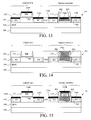
FIG. 13 is a cross-sectional diagram, following from FIG. 9, which illustrates an alternative embodiment wherein the dielectric filler layer has been removed, and a self-aligned silicide having been used to form source/drain contacts and a gate electrode contact in the CMOS FET device(s), and emitter/collect contacts and a base contact in the bipolar transistor device(s) according to an embodiment of the present invention;
FIG. 14 is a cross-sectional diagram, following from FIG. 9, which illustrates another alternative embodiment wherein epitaxy is used to thicken the base in the bipolar transistor device(s) according to an embodiment of the present invention; and
FIG. 15 is a cross-sectional diagram, following from FIG. 14, which illustrates the dielectric filler layer having been removed, and a self-aligned silicide having been used to form source/drain contacts and a gate electrode contact in the CMOS FET device(s), and emitter/collect contacts and a base contact in the bipolar transistor device(s) according to an embodiment of the present invention.
DETAILED DESCRIPTION OF PREFERRED EMBODIMENTS
Provided herein are techniques for fabricating lateral PNP or NPN bipolar transistors using a replacement gate-based process flow. Advantageously, the present techniques can be used in combination with either implant and/or solid source diffusion to make abrupt junction base regions. At the same time as forming the lateral bipolar regions, other regions can be processed with a replacement gate flow for CMOS field-effect transistors (FETs). Doing this allows for both bipolar devices and CMOS FETs on the same chip, allowing a designer to use either, whichever is best.
Further, conventional bipolar transistors have silicon (Si)-based designs. See, for example, U.S. patent application Ser. No. 13/607,877, filed by J. Sleight et al., entitled “A Lateral Bipolar Transistor and CMOS Hybrid Technology,” the entire contents of which are incorporated by reference herein. However, the use of materials other than Si can lead to design performance enhancements. For instance, III-V materials can have significantly higher electron mobility than Si.
The present techniques are now described by way of reference to FIGS. 1-15 which provide an exemplary methodology for co-fabricating a CMOS FET and a lateral bipolar transistor on a wafer. For illustrative purposes, the figures illustrate the formation of one CMOS FET and one lateral bipolar transistor. However, it is to be understood that multiple FETs and/or multiple bipolar transistors can be formed in the same manner as now described. Further, while the present bipolar transistor fabrication techniques are shown integrated with a CMOS FET process flow, if so desired the present techniques may be implemented, in the same manner described herein, to fabricate a bipolar transistor device(s) alone, i.e., independent of other devices on the wafer. Thus, it is to be understood that the depiction of the fabrication of a CMOS FET(s) and a bipolar transistor(s) concurrently on a wafer is only an example intended to show how the present techniques are compatible with a FET fabrication process.
As shown in FIG. 1 the starting platform for the process is a semiconductor wafer, such as a bulk semiconductor (e.g., silicon (Si), silicon germanium (SiGe), Ge, etc.) or semiconductor-on-insulator (SOD wafer. In the example depicted in FIG. 1, a SOI wafer 101 is employed. As shown in FIG. 1, the SOI wafer 101 includes an SOI layer 102 separated from a substrate 106 by a buried oxide (or BOX) 104.
The SOI layer 102 is formed from a semiconductor material including, but not limited to, Si, SiGe, Ge, and a III-V semiconductor material. The term III-V semiconductor material (or simply III-V material), as used herein and throughout the following description, refers to a material that includes at least one group III element and at least one group V element. By way of example only, suitable III-V materials include, but are not limited to, one or more of aluminum gallium arsenide, aluminum gallium nitride, aluminum indium arsenide, aluminum nitride, gallium antimonide, gallium arsenide, gallium nitride, indium antimonide, indium arsenide, indium gallium arsenide, indium gallium nitride, indium nitride, indium phosphide and combinations including at least one of the foregoing materials. According to an exemplary embodiment, the III-V material is indium gallium arsenide (InGaAs).
As highlighted above, by way of non-limiting example, the figures will depict the formation of one CMOS FET and one lateral bipolar transistor on the wafer. Accordingly, for clarity of depiction, these regions “CMOS FET” and “bipolar transistor” are shown labeled in the figures. Further, as shown in FIG. 1, the active regions of the wafer (i.e., in which the devices will be formed) are separated using standard isolation techniques, such as shallow trench isolation (STI).
As provided above, the present techniques utilize a replacement gate-based approach. Namely, as shown in FIG. 1, at least one dummy gate 108 is formed on the wafer in the CMOS FET region and at least one dummy gate 110 is formed on the wafer in the bipolar transistor region. As shown in FIG. 1, the dummy gates 108 and 110 are separated from the SOI layer 102 by a dummy gate dielectric.
According to an exemplary embodiment, the dummy gates are formed concurrently in the CMOS FET and bipolar transistor regions by first forming an interfacial oxide on the SOI layer 102 which will serve as the dummy gate dielectric. This oxide (e.g., silicon dioxide (SiO2)) can be deposited onto SOI layer 102, or grown from SOI layer 102 using an oxidation process, such as thermal oxidation. As will be described in detail below, the dummy gate oxide serves as an etch stop layer. Namely, during the dummy gate removal step (see below), the presence of an etch stop layer permits the dummy gate material to be removed selective to the underlying SOI.
Next, a suitable dummy gate material (e.g., poly-silicon) can then be blanket deposited onto the wafer, over the interfacial (dummy gate) oxide. Standard lithography and etching processes can then be performed to pattern the dummy gate material and interfacial oxide with the footprints and locations of the dummy gates, thus forming dummy gate 108 (and dummy gate oxide) in the CMOS FET region and dummy gate 110 (and dummy gate oxide) in the bipolar transistor region. As will become apparent from the description that follows, the dummy gate 108 is present over a portion of the wafer that serves as a channel region of the CMOS FET device, and the dummy gate 110 is present over a portion of the wafer that serves as a base of the bipolar FET device.
As shown in FIG. 1, spacers 112 and spacers 114 are then formed on opposite sides of the dummy gates 108 and 110, respectively. According to an exemplary embodiment, the spacers are formed concurrently in the CMOS FIT and bipolar transistor regions by first depositing a spacer material (e.g., a nitride material such as silicon nitride), and then patterning the material to form the spacers 112/114.
Next, the collector and emitter doping in the bipolar transistor region of the wafer is performed. See FIG. 2. In the case where a CMOS FET(s) are being fabricated on the same wafer (such as in the example of FIG. 2), it is preferable to first mask the CMOS FETs (e.g., using a resist or hardmask) to prevent doping in the FET devices. Suitable hardmask materials include, but are not limited to, nitride materials such as silicon nitride (SiN). Standard lithography and etching techniques can be used to pattern the mask.
As shown in FIG. 2, collector/emitter doping is then performed to form doped collector/emitter regions 202 (either N+ or P+) on both sides of the dummy gate 110. Conventional doping processes can be employed. Alternatively, the doping can be also be achieved using solid source diffusion. In either case, the dopant dose can be from about 5×10¹⁸ atoms/cm3 to about 5×10²⁰ atoms/cm3, e.g., from about 5×10¹⁹ atoms/cm3 to about 2×10²⁰ atoms/cm3. In an NPN bipolar transistor configuration, both sides of dummy the gate 110 can receive a number of successive implants of boron ions at various energies. In a PNP bipolar transistor configuration, both sides of the dummy gate 110 can receive successive implantation steps of either arsenic or phosphoric ions.
Following the collector/emitter doping, the mask can be removed from the CMOS FET device(s). The same general process can also be used dope source/drain regions 302 on both sides of the dummy gate 108. See FIG. 3. As shown in FIG. 3, a mask (e.g., resist or hardmask) can be formed covering the bipolar transistors (in the same manner as described above), and a conventional dopant implantation process can be used to form the source and drain regions 302 of the FET device(s). The order in which the collector/emitter (FIG. 2) and source/drain doping (FIG. 3) is performed is immaterial and these processes can be performed in either order. Following the source/drain doping, the mask can be removed from the bipolar transistor device(s).
Next, a dielectric filler layer 402 is blanket deposited onto the wafer, surrounding the dummy gates. See FIG. 4. As shown in FIG. 4, the dielectric filler layer 402 is then planarized down to a top of the dummy gates. This will permit removal of the dummy gates later in the process. Planarization of the dielectric filler layer 402 can be performed using chemical mechanical polishing (CMP).
In the description that follows, steps are provided first for forming an epitaxial material as the base of the bipolar transistor device(s) followed by replacement gate processing in the CMOS FET device(s). This sequence is presented only as an example. The steps described herein can be performed in any order, and in some cases steps can be performed concurrently with one another.
Thus, by way of example only, as shown in FIG. 5, the dummy gates 108 and 110 are next removed from the CMOS FET and bipolar transistor devices. The dummy gates 108 and 110 can be removed selective to the dielectric filler layer 402 and spacers 112/114 using wet chemical etching or dry etching. Removal of the dummy gates results in trenches being formed in the dielectric filler layer. In the case of the bipolar transistor device(s), removal of the dummy gate exposes the base.
In order to permit selective processing of the bipolar transistor device(s), following the dummy gate removal the CMOS FET device(s) are masked (e.g., with a resist or hardmask). See FIG. 6.
Next, the base in the bipolar transistor device(s) is/are recessed. See FIG. 6. This base recess can be performed using a selective etch, such as a selective reactive ion etching (RIE) process. The emitter and collector are covered/protected by the dielectric filler layer 402 and (as provided above) the CMOS FET device(s) are masked.
A RIE process, for example, is anisotropic and if employed will result in portions of the (SOI) base below/masked by the spacers 114 to remain following the base recess etch. See FIG. 6. Further, the etch should be endpointed prior to removing all of the (SOI) at the bottom of the base. These remaining portions of the SOI at the bottom and sides of the base will be used to template re-growth of the base using SiGe, Ge or a III-V semiconductor material.
Namely, as shown in FIG. 7, epitaxial re-growth of the base in the bipolar transistor device(s) is next performed. According to an exemplary embodiment, the base is re-grown at this stage from an epitaxial SiGe, Ge or III-V semiconductor material 702. Re-growth of the base material permits the base to be formed from a different material than the collector and emitter regions (i.e., that of the SOI layer 102). In fact, the material from which to re-grow the base is preferably chosen such that the bandgap in the base is smaller than the bandgap of the collector/emitter. As provided above, the collector/emitter regions are formed from doped portions of the SOI layer 102. As also provided above, the SOI layer can be formed from a semiconductor material, such as Si, SiGe, Ge, and a III-V semiconductor material. Thus, depending on the contents of SOI layer 102, the base is preferably re-grown from a material with a lower bandgap than the SOI layer. Bandgap data for each of the above-described SOI and base materials may be found in the published literature. See, for instance, Helmut Foll, “Semiconductors 1, 5.1.4 Wavelength Engineering” Kiel University, Germany (accessed on Aug. 14, 2013) (which on page 1 of section 5.1.4 provides bangap and lattice constant data for a variety of different materials, including Si, Ge, and III-V materials) (hereinafter “Foll”), the entire contents of which are incorporated by reference herein. In the bandgap charts provided in Foll, the lines represent alloys of the materials. Thus one can adjust the bandgap along those lines. Therefore, selection of the SOI and base materials can be performed accordingly. To use a simple example, if the collector and emitter regions (based on the composition of SOI layer 102) are formed from gallium arsenide, then a suitable choice for the base might be epitaxial Ge, since Ge has a lower bandgap than gallium arsenide (see Foll).
Further, the base can be doped in-situ during this re-growth process. Suitable dopants include, but are not limited to boron (p-type) and phosphorous (n-type). By way of example only, a suitable base doping concentration is from about 1×1017 cm3 to about 1×1018 cm3, e.g., from about 2×1017 cm3 to about 5×1017 cm3. It is notable that doping the base at this stage is optional, and the base can be doped later in the process.
When in-situ doping is performed, as shown in FIG. 7, some dopant out-diffusion is preferable to move the depletion region away from the re-growth interface. Base dopant out-diffusion is described generally in Li et al., “The base dopant out diffusion and the optimized setback layers in SiGe HBT,” Proceedings from the 6th International Conference on Solid-State and Integrated-Circuit Technology 2001, vol. 1, pgs. 596-599 (October 2001), the entire contents of which are incorporated by reference herein. Out-diffusion can be accomplished using an anneal to “out-diffuse” the dopant(s).
Moving the depletion region away from the re-growth interface (e.g., via out-diffusion) is important since the (epitaxial) re-growth interface is the location most likely to contain crystal defects caused by factors such as like lattice mismatch. A small amount of lattice mismatch can be tolerated and results in elastic deformation of the materials (strain sharing). A large amount of lattice mismatch however results in plastic deformation (defects) such as so-called misfit defects. Defects in the depletion region act as carrier generation/recombination centers that reduce the gain of bipolar transistors. So, an anneal that moves the doping far enough that the defects are in a quasi-neutral region is advantageous. The amount of diffusion depends on the width of the depletion region which depends on the doping concentration and the applied biases, as so:
W [ 2 ε r ε 0 q ( N A + N D N A N D ) ( V bi - V ) ] 1 2
By way of example only, when the collector/emitter are highly doped (e.g., as per the exemplary collector and emitter doping concentrations provided in conjunction with the description of FIG. 2, above) the depletion region is preferably moved a distance of less than about 10 nanometers (nm) (e.g., from about 1 nm to about 8 nm) away from the re-growth interface. To use an illustrative, non-limiting example: when the base material is epitaxial Si or SiGe, an anneal at a temperature of from about 900° C. to about 1,000° C. (e.g., about 950° C.) for a duration of from about 5 seconds to about 10 seconds, would move the depletion region the above-described distance away from the re-growth interface.
Hereinafter, the base including doped epitaxial SiGe, Ge or III-V (and associated out-diffusion region) or epitaxial SiGe, Ge or III-V doped later in the process using, e.g., solid-source diffusion (see below) will be given reference numeral 702.
As shown in FIG. 8, optional inner spacers 802 can be formed in the bipolar transistor device(s). Placing spacers 802 between what will be the collector/emitter regions of the device and the device contact will help to minimize parasitic capacitance in the completed device. According to an exemplary embodiment, spacers 802 are formed by first depositing a nitride layer into the trench. A resist film is then deposited on the nitride layer, masked and patterned with the spacer footprints. A nitride-selective RIE is then used to define spacers in the nitride layer. The CMOS FET device(s) remain masked during this inner spacer formation process. The remainder of the steps of the process will be illustrated in the figures with the optional inner spacers present, however the same steps would be performed, in the same manner described, whether or not the inner spacers 802 are present.
According to the instant example, processing of the CMOS FET device(s) is now conducted in order to form a replacement gate in the FET device(s). To do so, any masking present over the CMOS FET device(s) is removed. As described above, in this example, the dummy gate has already been removed selective to the dielectric filler layer and spacers. This step (illustrated in FIG. 5) was performed concurrently in both the CMOS FET and bipolar transistor devices. However, it is possible to leave the CMOS FET dummy gate(s) in place until this point when the replacement gate is formed. Regardless, removal of the dummy gate(s) in the CMOS FET device(s) results in a trench(es) being formed in the dielectric filler layer.
As shown in FIG. 9, masking (e.g., resist or hardmask) is first needed to block off the bipolar transistor device(s) during the CMOS FET replacement gate process. Next a replacement gate stack(s) is/are formed in the trench(es) in the dielectric filler layer over the CMOS FET device(s). According to an exemplary embodiment, the replacement gate stack(s) include a gate dielectric 902 and a gate electrode 904. The gate dielectric separates the gate electrode from the portion of the SOI that will serve as a channel region of the CMOS FET device(s). In general, each FET will include a source region and a drain region interconnected by a channel region, and a gate electrode over the channel region that regulates electron flow through the channel.
The gate electrode can be formed from a metal or combination of metals and/or doped polysilicon. For a metal gate, a high-k dielectric, such as hafnium oxide, is preferred. As provided above, a dummy gate dielectric was employed as an etch stop earlier in the process. Any of this dummy gate dielectric remaining is preferably removed and replaced with the gate dielectric 902. Following formation of the replacement gate stack(s) in the CMOS FET device(s), the masking over the bipolar transistor device(s) can be removed.
As provided above, the base region(s) of the bipolar transistor device(s) may have already been doped, in situ, during re-growth of the (SiGe, Ge, or III-V) base material. If so, then the process now described for doping the base is unnecessary. On the other hand, if the base is yet undoped, then according to an exemplary embodiment, the base region(s) of the bipolar transistor device(s) are now doped using either solid source diffusion or doping agent implant. With solid source diffusion, a dopant-containing material (the solid source) is deposited on the semiconductor to be doped. Suitable dopant-containing materials include, but are not limited to, borosilicate glass (BSG), phospho-silicate glass (PSG), and doped germanium. An anneal is then performed at a temperature of from about 900° C. to about 1,000° C. to allow the dopants in the dopant-containing material or solid-source to diffuse into the semiconductor. The solid source can then be removed using, for example, a hydrofluoric acid (HF) dip. Alternatively, the base implant doping can be applied at an angle to the perpendicular to fine tune the desired base-collector doping level gradient. According to an exemplary embodiment, suitable doping agents include, but are not limited to, boron (p-type) or phosphorous (n-type).
Next, a gate electrode contact is formed in the CMOS FET device(s) and a base contact is formed in the bipolar FET device(s). While the following description and related figures describe these contact-forming processes as being performed concurrently in the CMOS FET and bipolar transistor devices, it is of course possible to process the devices separately, using selective masking as described above. To begin the contact formation process, a layer of polysilicon 1002 is blanket deposited onto the wafer, covering the CMOS FET device(s) and bipolar transistor devices. See FIG. 10. According to an exemplary embodiment, the polysilicon layer 1002 is deposited to a thickness of from about 5 nanometers (nm) to about 30 nm, e.g., from about 10 nm to about 15 nm.
Standard lithography and etching techniques are then used to pattern the polysilicon layer 1002, to remove the polysilicon layer from over all but the gate electrode 904 in the CMOS FET device(s) and the base 702 of the bipolar transistor device(s). For clarity of description, these remaining portions of the polysilicon layer are hereinafter referred to herein by the reference numerals 1002 a and 1002 b, respectively. See FIG. 11. As shown in FIG. 11, the patterned polysilicon layer 1002 a and 1002 b covering the spacers preferably remains.
A self-aligned silicide (a salicide) is then formed to produce gate electrode and base contacts 1202 a and 1202 b in the CMOS FET and bipolar transistor devices, respectively. See FIG. 12. To begin the salicide process, a silicide metal is first blanket deposited onto the wafer (using, e.g., sputtering, evaporation, etc.). Suitable silicide metals include, but are not limited to, nickel, platinum, and combinations thereof such as nickel platinum. The process is self-aligned since the silicide will form only in areas where the silicide metal is in contact with the semiconductor (in this case the polysilicon 1002 a and 1002 b).
Next, an anneal is performed, for example, at a temperature of from about 500° C. to about 1,100° C. for a duration of from about 5 seconds to about 10 seconds, to react the metal with the semiconductor forming a metal silicide. This metal silicide forms the gate electrode and base contacts 1202 a and 1202 b in the CMOS FET and bipolar transistor devices, respectively. Any unreacted metal can be stripped using a wet etching process. While this silicidation process is generally described herein as a one step anneal (e.g., deposit metal, anneal, strip unreacted metal), it is possible and in some cases preferable to employ a multi-step annealing process (e.g., deposit metal, anneal at a first temperature, strip metal, anneal at a second, higher temperature).
As shown in FIG. 12, a portion of the polysilicon 1002 a/1002 b can remain under the silicide of the contacts 1202 a and 1202 b. The amount of silicide formed can be controlled based on one or more of the amount of metal deposited, the anneal temperature, duration, etc.
The above-described process is merely one example of how CMOS FETs and bipolar transistor devices can be co-fabricated on a wafer. As provided above, co-fabrication is also an exemplary implementation of the present techniques, as the above-described process can be used in the same manner to fabricate solely CMOS FETS or (SiGe, Ge, III-V material-based) bipolar transistors. Further, some notable alternative steps to the above-described process can be employed. These alternative embodiments are now described.
For example, in one alternative embodiment, the silicidation contact-forming process is used, in addition to forming the gate electrode and base contacts as described above, to also form source/drain and emitter/collector contacts. Namely, following from FIG. 9, the dielectric filler layer 402 is in this case removed (using, e.g., a wet or dry etch). See FIG. 13.
Following removal of the dielectric filler layer, a self-aligned silicide (a salicide) is used to (concurrently) form in the CMOS FET device(s): source/drain contacts 1302 and gate electrode contact 1304, and in the bipolar transistor device(s): emitter/collect contacts 1306 and base contact 1308. It is notable that in order for the gate electrode contact 1304 to be formed by this silicidation process, the (replacement) gate electrode 904 has to include a semiconductor material (such as polysilicon).
In the same manner as described above, to begin the silicidation process, a silicide metal (e.g., nickel, platinum, nickel platinum, etc.) is first blanket deposited onto the wafer. The process is self-aligned since the silicide will form only in areas where the silicide metal is in contact with the semiconductor (in this case the CMOS FET source, drain, and gate electrode, and the bipolar transistor collector, emitter and base).
Next, an anneal is performed, for example, at a temperature of from about 500° C. to about 1,100° C., for a duration of from about 5 seconds to about 10 seconds, to react the metal with the semiconductor forming a metal silicide. Any unreacted metal can be stripped using a wet etching process. As provided above, the silicidation can be performed as a one or multi-step annealing process.
In yet another exemplary alternative embodiment, the same process as illustrated in FIG. 13 is performed to form CMOS FET source/drain and gate electrode contacts, and bipolar transistor emitter/collector and base contacts, however prior to removal of the dielectric filler layer epitaxy is used to build up the bipolar transistor base. Namely, again starting with the structure of FIG. 9, epitaxy is used to thicken the base 702. It is notable that by this stage in the process the base 702 has already been doped, see above. Here, the epitaxy is being used simply to thicken the base. According to an exemplary embodiment, epitaxial SiGe, Ge or a III-V semiconductor material is grown over base 702. Any excess epitaxial material can be removed (e.g., using chemical mechanical polishing (CMP)) such that the remaining extended base 1402 is flush with the dielectric filler layer. See FIG. 14.
Next, in the same manner as described in conjunction with the description of FIG. 13, above, the dielectric filler layer is removed (using wet or dry etching) and a self-aligned silicide (a salicide) is used to (concurrently) form in the CMOS FET device(s): source/drain contacts 1502 and gate electrode contact 1504, and in the bipolar transistor device(s): emitter/collect contacts 1506 and base contact 1508. See FIG. 15.
Although illustrative embodiments of the present invention have been described herein, it is to be understood that the invention is not limited to those precise embodiments, and that various other changes and modifications may be made by one skilled in the art without departing from the scope of the invention.

Claims (10)

What is claimed is:
1. A method of co-fabricating at least one CMOS FET device and at least one bipolar transistor device on a wafer, the method comprising the steps of:
forming at least one CMOS FET dummy gate and at least one bipolar transistor dummy gate on the wafer, wherein the CMOS FET dummy gate is present over a portion of the wafer that serves as a channel region of the CMOS FET device and the bipolar transistor dummy gate is present over a portion of the wafer that serves as a base of the bipolar transistor;
doping the wafer to form emitter and collector regions on both sides of the bipolar transistor dummy gate;
doping the wafer to form source and drain regions on both sides of the CMOS FET dummy gate;
depositing a dielectric filler layer onto the wafer surrounding the CMOS FET dummy gate and the bipolar transistor dummy gate;
removing the CMOS FET dummy gate and the bipolar transistor dummy gate selective to the dielectric filler layer, wherein removal of the CMOS FET dummy gate results in at least one first trench being formed in the dielectric filler layer and removal of the bipolar transistor dummy gate results in at least one second trench being formed in the dielectric filler layer;
recessing the base of the bipolar transistor;
re-growing the base of the bipolar transistor from an epitaxial material selected from the group consisting of: SiGe, Ge, and a III-V material;
forming a replacement gate of the CMOS FET device in the first trench over the channel region of the CMOS FET device; and
forming contacts to the replacement gate of the CMOS FET device and to the base of the bipolar transistor device.
2. The method of claim 1, further comprising the step of:
forming spacers on opposite sides of the CMOS FET dummy gate and on opposite sides of the bipolar transistor dummy gate.
3. The method of claim 2, further comprising the step of
forming inner spacers in the bipolar transistor device.
4. The method of claim 1, wherein the base of the bipolar transistor is re-grown from a III-V epitaxial material selected from the group consisting of aluminum gallium arsenide, aluminum gallium nitride, aluminum indium arsenide, aluminum nitride, gallium antimonide, gallium arsenide, gallium nitride, indium antimonide, indium arsenide, indium gallium arsenide, indium gallium nitride, indium nitride, indium phosphide and combinations comprising at least one of the foregoing materials.
5. The method of claim 1, further comprising the step of:
doping the base of the bipolar transistor, in situ, during re-growth of the base from the epitaxial material.
6. The method of claim 1, further comprising the step of:
doping the base of the bipolar transistor using solid source diffusion.
7. The method of claim 1, wherein the step of forming contacts to the replacement gate of the CMOS FET device and to the base of the bipolar transistor device comprises the steps of
depositing a polysilicon layer onto the wafer covering the CMOS FET device and the bipolar transistor device;
patterning the polysilicon layer such that the polysilicon layer remains only on the replacement gate of the CMOS FET device and on the base of the bipolar transistor;
depositing a metal onto the wafer;
reacting the metal with the patterned polysilicon layer to form the contacts to the replacement gate of the CMOS FET device and to the base of the bipolar transistor device; and
removing any unreacted metal.
8. The method of claim 1, further comprising the step of:
forming contacts to the source and drain regions of the CMOS FET device and to the emitter and collector regions of the bipolar transistor device.
9. The method of claim 8, further comprising the steps of:
removing the dielectric filler layer;
depositing a metal onto the wafer;
reacting the metal with the source and drain regions to form the contacts to the source and drain regions of the CMOS FET device and reacting the metal with the emitter and collector regions to form the contacts to the emitter and collector regions of the bipolar transistor device.
10. The method of claim 9, further comprising the step of:
thickening the base of the bipolar transistor device using epitaxy.
US15/332,207 2014-04-04 2016-10-24 III-V, SiGe, or Ge base lateral bipolar transistor and CMOS hybrid technology Active US9812370B2 (en)

Priority Applications (1)

Application Number Priority Date Filing Date Title
US15/332,207 US9812370B2 (en) 2014-04-04 2016-10-24 III-V, SiGe, or Ge base lateral bipolar transistor and CMOS hybrid technology

Applications Claiming Priority (2)

Application Number Priority Date Filing Date Title
US14/245,627 US9496184B2 (en) 2014-04-04 2014-04-04 III-V, SiGe, or Ge base lateral bipolar transistor and CMOS hybrid technology
US15/332,207 US9812370B2 (en) 2014-04-04 2016-10-24 III-V, SiGe, or Ge base lateral bipolar transistor and CMOS hybrid technology

Related Parent Applications (1)

Application Number Title Priority Date Filing Date
US14/245,627 Division US9496184B2 (en) 2014-04-04 2014-04-04 III-V, SiGe, or Ge base lateral bipolar transistor and CMOS hybrid technology

Publications (2)

Publication Number Publication Date
US20170040219A1 US20170040219A1 (en) 2017-02-09
US9812370B2 true US9812370B2 (en) 2017-11-07

Family

ID=54210394

Family Applications (2)

Application Number Title Priority Date Filing Date
US14/245,627 Expired - Fee Related US9496184B2 (en) 2014-04-04 2014-04-04 III-V, SiGe, or Ge base lateral bipolar transistor and CMOS hybrid technology
US15/332,207 Active US9812370B2 (en) 2014-04-04 2016-10-24 III-V, SiGe, or Ge base lateral bipolar transistor and CMOS hybrid technology

Family Applications Before (1)

Application Number Title Priority Date Filing Date
US14/245,627 Expired - Fee Related US9496184B2 (en) 2014-04-04 2014-04-04 III-V, SiGe, or Ge base lateral bipolar transistor and CMOS hybrid technology

Country Status (1)

Country Link
US (2) US9496184B2 (en)

Cited By (6)

* Cited by examiner, † Cited by third party
Publication number Priority date Publication date Assignee Title
US10037989B1 (en) * 2017-10-26 2018-07-31 International Business Machines Corporation III-V lateral bipolar integration with silicon
US10707336B1 (en) 2019-02-26 2020-07-07 International Business Machines Corporation High-performance lateral BJT with epitaxial lightly doped intrinsic base
US10784347B1 (en) 2019-03-07 2020-09-22 International Business Machines Corporation High-performance lateral BJT with epitaxial lightly doped intrinsic base
US11195766B2 (en) * 2017-09-13 2021-12-07 Infineon Technologies Ag Manufacturing a combined semiconductor device
RU2767597C1 (en) * 2021-05-21 2022-03-17 Российская Федерация, от имени которой выступает Государственная корпорация по атомной энергии "Росатом" Lateral bipolar transistor based on “silicon on insulator” structures and the method for its manufacture
US11949004B2 (en) 2021-08-27 2024-04-02 Globalfoundries U.S. Inc. Lateral bipolar transistors with gate structure aligned to extrinsic base

Families Citing this family (14)

* Cited by examiner, † Cited by third party
Publication number Priority date Publication date Assignee Title
US9525027B2 (en) * 2014-03-13 2016-12-20 Globalfoundries Inc. Lateral bipolar junction transistor having graded SiGe base
US9721969B2 (en) * 2015-06-30 2017-08-01 Globalfoundries Singapore Pte. Ltd. Creation of wide band gap material for integration to SOI thereof
US9761480B1 (en) * 2016-02-18 2017-09-12 Globalfoundries Inc. Methods of forming field effect transistor (FET) and non-FET circuit elements on a semiconductor-on-insulator substrate
US9472471B1 (en) * 2016-03-01 2016-10-18 International Business Machines Corporation Hybrid orientation vertically stacked III-V and Ge gate-all-around CMOS
US9953125B2 (en) 2016-06-15 2018-04-24 International Business Machines Corporation Design/technology co-optimization platform for high-mobility channels CMOS technology
US9786656B1 (en) 2016-08-19 2017-10-10 International Business Machines Corporation Integration of bipolar transistor into complimentary metal-oxide-semiconductor process
US9991254B1 (en) * 2017-03-09 2018-06-05 International Business Machines Corporation Forming horizontal bipolar junction transistor compatible with nanosheets
US10347667B2 (en) * 2017-07-26 2019-07-09 International Business Machines Corporation Thin-film negative differential resistance and neuronal circuit
US10622262B2 (en) 2017-10-06 2020-04-14 Newport Fab Llc High performance SiGe heterojunction bipolar transistors built on thin film silicon-on-insulator substrates for radio frequency applications
US10580900B2 (en) 2018-01-19 2020-03-03 International Business Machines Corporation Nanosheet channel post replacement gate process
US11094599B2 (en) * 2018-06-28 2021-08-17 United Microelectronics Corp. Semiconductor structure and manufacturing method thereof
US11276770B2 (en) * 2019-11-05 2022-03-15 Globalfoundries U.S. Inc. Gate controlled lateral bipolar junction/heterojunction transistors
US11488950B2 (en) 2021-02-11 2022-11-01 Globalfoundries U.S. Inc. Integrated circuit structure and method for bipolar transistor stack within substrate
US11894450B2 (en) * 2021-11-18 2024-02-06 Globalfoundries U.S. Inc. Lateral bipolar transistor with emitter and collector regions including portions within In-insulator layer cavities and method

Citations (15)

* Cited by examiner, † Cited by third party
Publication number Priority date Publication date Assignee Title
US20100047987A1 (en) 2005-04-28 2010-02-25 Nxp B.V. Method of fabricating a bipolar transistor
US7671447B2 (en) 2004-07-15 2010-03-02 Nxp B.V. Bipolar transistor and method of manufacturing the same
US7772060B2 (en) 2006-06-21 2010-08-10 Texas Instruments Deutschland Gmbh Integrated SiGe NMOS and PMOS transistors
CN102592998A (en) 2012-03-22 2012-07-18 中国科学院上海微系统与信息技术研究所 SOI-based longitudinal SiGe bipolar transistor and a preparation method thereof
CN102723361A (en) 2012-07-16 2012-10-10 西安电子科技大学 Self-aligned-technology-based tri-polycrystal SOI (Silicon On Insulator), SiGe and HBT (Heterojunction Bipolar Transistor) integrated device and preparation method thereof
CN102738158A (en) 2012-07-16 2012-10-17 西安电子科技大学 Strain Si Bi CMOS (complementary metal-oxide-semiconductor transistor) integrated device based on autocollimation technology and manufacturing method thereof
CN102738160A (en) 2012-07-16 2012-10-17 西安电子科技大学 Mixed crystal plane silicon-on-insulator (SOI) bipolar complementary metal oxide semiconductor (BiCMOS) integrated device based on square channel process and preparation method
CN102738178A (en) 2012-07-16 2012-10-17 西安电子科技大学 Double-polysilicon SOI (Silicon On Insulator) SiGe HBT (Heterojunction Bipolar Transistor) integrated device based on self-aligned technology and preparation method thereof
CN102751292A (en) 2012-07-16 2012-10-24 西安电子科技大学 Three-polycrystalline SiGe HBT (Heterojunction Bipolar Transistor)-based hybrid crystal face strain BiCOMS integrated device and preparation method thereof
US8329541B2 (en) 2007-06-15 2012-12-11 Taiwan Semiconductor Manufacturing Company, Ltd. InP-based transistor fabrication
US20120314485A1 (en) 2011-06-12 2012-12-13 International Business Machines Corporation Complementary soi lateral bipolar for sram in a low-voltage cmos platform
US8497169B2 (en) 2009-04-22 2013-07-30 Taiwan Semiconductor Manufacturing Company, Ltd. Method for protecting a gate structure during contact formation
US8709890B2 (en) 2011-12-12 2014-04-29 International Business Machines Corporation Method and structure for forming ETSOI capacitors, diodes, resistors and back gate contacts
US20150263168A1 (en) * 2014-03-13 2015-09-17 Taiwan Semiconductor Manufacturing Company, Ltd. Structure and Method for Semiconductor Device
US9525027B2 (en) * 2014-03-13 2016-12-20 Globalfoundries Inc. Lateral bipolar junction transistor having graded SiGe base

Patent Citations (15)

* Cited by examiner, † Cited by third party
Publication number Priority date Publication date Assignee Title
US7671447B2 (en) 2004-07-15 2010-03-02 Nxp B.V. Bipolar transistor and method of manufacturing the same
US20100047987A1 (en) 2005-04-28 2010-02-25 Nxp B.V. Method of fabricating a bipolar transistor
US7772060B2 (en) 2006-06-21 2010-08-10 Texas Instruments Deutschland Gmbh Integrated SiGe NMOS and PMOS transistors
US8329541B2 (en) 2007-06-15 2012-12-11 Taiwan Semiconductor Manufacturing Company, Ltd. InP-based transistor fabrication
US8497169B2 (en) 2009-04-22 2013-07-30 Taiwan Semiconductor Manufacturing Company, Ltd. Method for protecting a gate structure during contact formation
US20120314485A1 (en) 2011-06-12 2012-12-13 International Business Machines Corporation Complementary soi lateral bipolar for sram in a low-voltage cmos platform
US8709890B2 (en) 2011-12-12 2014-04-29 International Business Machines Corporation Method and structure for forming ETSOI capacitors, diodes, resistors and back gate contacts
CN102592998A (en) 2012-03-22 2012-07-18 中国科学院上海微系统与信息技术研究所 SOI-based longitudinal SiGe bipolar transistor and a preparation method thereof
CN102751292A (en) 2012-07-16 2012-10-24 西安电子科技大学 Three-polycrystalline SiGe HBT (Heterojunction Bipolar Transistor)-based hybrid crystal face strain BiCOMS integrated device and preparation method thereof
CN102738178A (en) 2012-07-16 2012-10-17 西安电子科技大学 Double-polysilicon SOI (Silicon On Insulator) SiGe HBT (Heterojunction Bipolar Transistor) integrated device based on self-aligned technology and preparation method thereof
CN102738160A (en) 2012-07-16 2012-10-17 西安电子科技大学 Mixed crystal plane silicon-on-insulator (SOI) bipolar complementary metal oxide semiconductor (BiCMOS) integrated device based on square channel process and preparation method
CN102738158A (en) 2012-07-16 2012-10-17 西安电子科技大学 Strain Si Bi CMOS (complementary metal-oxide-semiconductor transistor) integrated device based on autocollimation technology and manufacturing method thereof
CN102723361A (en) 2012-07-16 2012-10-10 西安电子科技大学 Self-aligned-technology-based tri-polycrystal SOI (Silicon On Insulator), SiGe and HBT (Heterojunction Bipolar Transistor) integrated device and preparation method thereof
US20150263168A1 (en) * 2014-03-13 2015-09-17 Taiwan Semiconductor Manufacturing Company, Ltd. Structure and Method for Semiconductor Device
US9525027B2 (en) * 2014-03-13 2016-12-20 Globalfoundries Inc. Lateral bipolar junction transistor having graded SiGe base

Non-Patent Citations (9)

* Cited by examiner, † Cited by third party
Title
Computer translation of CN102592998 (Feb. 2013).
Computer translation of CN102723361 (Feb. 2013).
Computer translation of CN102738158 (Feb. 2013).
Computer translation of CN102738160 (Feb. 2013).
Computer translation of CN102738178 (Feb. 2013).
Computer translation of CN102751292 (Feb. 2013).
Helmut Foll, "Semiconductors I, 5.1.4 Wavelength Engineering" Kiel University, Germany (accessed on Aug. 14, 2013).
Li et al., "The base dopant out diffusion and the optimized setback layers in SiGe HBT," Proceedings from the 6th International Conference on Solid-State and Integrated-Circuit Technology 2001, vol. 1, pp. 596-599 (Oct. 2001).
List of IBM Patents or Applications Treated as Related.

Cited By (6)

* Cited by examiner, † Cited by third party
Publication number Priority date Publication date Assignee Title
US11195766B2 (en) * 2017-09-13 2021-12-07 Infineon Technologies Ag Manufacturing a combined semiconductor device
US10037989B1 (en) * 2017-10-26 2018-07-31 International Business Machines Corporation III-V lateral bipolar integration with silicon
US10707336B1 (en) 2019-02-26 2020-07-07 International Business Machines Corporation High-performance lateral BJT with epitaxial lightly doped intrinsic base
US10784347B1 (en) 2019-03-07 2020-09-22 International Business Machines Corporation High-performance lateral BJT with epitaxial lightly doped intrinsic base
RU2767597C1 (en) * 2021-05-21 2022-03-17 Российская Федерация, от имени которой выступает Государственная корпорация по атомной энергии "Росатом" Lateral bipolar transistor based on “silicon on insulator” structures and the method for its manufacture
US11949004B2 (en) 2021-08-27 2024-04-02 Globalfoundries U.S. Inc. Lateral bipolar transistors with gate structure aligned to extrinsic base

Also Published As

Publication number Publication date
US20170040219A1 (en) 2017-02-09
US9496184B2 (en) 2016-11-15
US20150287642A1 (en) 2015-10-08

Similar Documents

Publication Publication Date Title
US9812370B2 (en) III-V, SiGe, or Ge base lateral bipolar transistor and CMOS hybrid technology
US9209095B2 (en) III-V, Ge, or SiGe fin base lateral bipolar transistor structure and method
US10312151B1 (en) Monolithic co-integration of MOSFET and JFET for neuromorphic/cognitive circuit applications
US20090174002A1 (en) Mosfet having a high stress in the channel region
US8440552B1 (en) Method to form low series resistance transistor devices on silicon on insulator layer
US20060244073A1 (en) FABRICATION OF AN EEPROM CELL WITH SiGe SOURCE/DRAIN REGIONS
CN103489863A (en) Homo-junction diode structures using fin field effect transistor processing
US20120080754A1 (en) Semiconductor device and method of manufacturing semiconductor device
US10957776B2 (en) Method of fabricating MOSFET
US9159816B2 (en) PNP bipolar junction transistor fabrication using selective epitaxy
US10014397B1 (en) Bipolar junction transistors with a combined vertical-lateral architecture
US10332983B1 (en) Vertical field-effect transistors including uniform gate lengths
US9634103B2 (en) CMOS in situ doped flow with independently tunable spacer thickness
US8138547B2 (en) MOSFET on silicon-on-insulator REDX with asymmetric source-drain contacts
US20190214313A1 (en) Local wiring in between stacked devices
US9496262B2 (en) High mobility transistors
US8999805B1 (en) Semiconductor device with reduced gate length
JPH04221835A (en) Bipolar transistor and manufacture thereof
US11244870B2 (en) Maskless top source/drain epitaxial growth on vertical transport field effect transistor
US20170092749A1 (en) Semiconductor-on-insulator lateral heterojunction bipolar transistor having epitaxially grown intrinsic base and deposited extrinsic base
US7696025B2 (en) Sidewall semiconductor transistors
US9105650B2 (en) Lateral bipolar transistor and CMOS hybrid technology
US6184099B1 (en) Low cost deep sub-micron CMOS process
US20080280414A1 (en) Systems and Methods for Fabricating Vertical Bipolar Devices
JP3938569B2 (en) Manufacturing method of semiconductor integrated circuit device

Legal Events

Date Code Title Description
AS Assignment

Owner name: INTERNATIONAL BUSINESS MACHINES CORPORATION, NEW Y

Free format text: ASSIGNMENT OF ASSIGNORS INTEREST;ASSIGNORS:CHANG, JOSEPHINE B.;LAUER, GEN P.;LAUER, ISAAC;AND OTHERS;SIGNING DATES FROM 20140331 TO 20140402;REEL/FRAME:040102/0190

STCF Information on status: patent grant

Free format text: PATENTED CASE

AS Assignment

Owner name: ELPIS TECHNOLOGIES INC., CANADA

Free format text: ASSIGNMENT OF ASSIGNORS INTEREST;ASSIGNOR:INTERNATIONAL BUSINESS MACHINES CORPORATION;REEL/FRAME:052620/0961

Effective date: 20200306

FEPP Fee payment procedure

Free format text: MAINTENANCE FEE REMINDER MAILED (ORIGINAL EVENT CODE: REM.); ENTITY STATUS OF PATENT OWNER: LARGE ENTITY

FEPP Fee payment procedure

Free format text: SURCHARGE FOR LATE PAYMENT, LARGE ENTITY (ORIGINAL EVENT CODE: M1554); ENTITY STATUS OF PATENT OWNER: LARGE ENTITY

MAFP Maintenance fee payment

Free format text: PAYMENT OF MAINTENANCE FEE, 4TH YEAR, LARGE ENTITY (ORIGINAL EVENT CODE: M1551); ENTITY STATUS OF PATENT OWNER: LARGE ENTITY

Year of fee payment: 4