US9805860B2 - Magnetic device and method of manufacturing the same - Google Patents
Magnetic device and method of manufacturing the same Download PDFInfo
- Publication number
- US9805860B2 US9805860B2 US15/409,549 US201715409549A US9805860B2 US 9805860 B2 US9805860 B2 US 9805860B2 US 201715409549 A US201715409549 A US 201715409549A US 9805860 B2 US9805860 B2 US 9805860B2
- Authority
- US
- United States
- Prior art keywords
- conductive part
- opening
- disposed
- core body
- coil
- Prior art date
- Legal status (The legal status is an assumption and is not a legal conclusion. Google has not performed a legal analysis and makes no representation as to the accuracy of the status listed.)
- Active
Links
- 238000004519 manufacturing process Methods 0.000 title description 4
- 238000000465 moulding Methods 0.000 claims description 23
- 238000005476 soldering Methods 0.000 claims description 6
- 239000007769 metal material Substances 0.000 claims 3
- 238000000034 method Methods 0.000 description 18
- 238000009713 electroplating Methods 0.000 description 16
- 238000005530 etching Methods 0.000 description 10
- 239000000843 powder Substances 0.000 description 8
- 238000005516 engineering process Methods 0.000 description 6
- 229910000859 α-Fe Inorganic materials 0.000 description 6
- XEEYBQQBJWHFJM-UHFFFAOYSA-N Iron Chemical group [Fe] XEEYBQQBJWHFJM-UHFFFAOYSA-N 0.000 description 5
- 238000007639 printing Methods 0.000 description 5
- 230000008901 benefit Effects 0.000 description 4
- 238000007731 hot pressing Methods 0.000 description 4
- 239000006247 magnetic powder Substances 0.000 description 4
- 239000000463 material Substances 0.000 description 4
- 238000003825 pressing Methods 0.000 description 4
- 238000005452 bending Methods 0.000 description 3
- 239000004020 conductor Substances 0.000 description 3
- 239000010949 copper Substances 0.000 description 3
- 239000000047 product Substances 0.000 description 3
- RYGMFSIKBFXOCR-UHFFFAOYSA-N Copper Chemical compound [Cu] RYGMFSIKBFXOCR-UHFFFAOYSA-N 0.000 description 2
- 229910019819 Cr—Si Inorganic materials 0.000 description 2
- 229910000640 Fe alloy Inorganic materials 0.000 description 2
- 229910018605 Ni—Zn Inorganic materials 0.000 description 2
- 229910002796 Si–Al Inorganic materials 0.000 description 2
- 239000000853 adhesive Substances 0.000 description 2
- 230000001070 adhesive effect Effects 0.000 description 2
- 229910000808 amorphous metal alloy Inorganic materials 0.000 description 2
- 229910052802 copper Inorganic materials 0.000 description 2
- 239000011889 copper foil Substances 0.000 description 2
- 238000010438 heat treatment Methods 0.000 description 2
- 238000012986 modification Methods 0.000 description 2
- 230000004048 modification Effects 0.000 description 2
- 229910052709 silver Inorganic materials 0.000 description 2
- 238000005245 sintering Methods 0.000 description 2
- 239000000758 substrate Substances 0.000 description 2
- 238000009966 trimming Methods 0.000 description 2
- 238000003466 welding Methods 0.000 description 2
- 239000012467 final product Substances 0.000 description 1
- 239000012778 molding material Substances 0.000 description 1
- 229910052759 nickel Inorganic materials 0.000 description 1
- 238000004080 punching Methods 0.000 description 1
- 229910052718 tin Inorganic materials 0.000 description 1
Images


Classifications
-
- H—ELECTRICITY
- H01—ELECTRIC ELEMENTS
- H01F—MAGNETS; INDUCTANCES; TRANSFORMERS; SELECTION OF MATERIALS FOR THEIR MAGNETIC PROPERTIES
- H01F17/00—Fixed inductances of the signal type
- H01F17/04—Fixed inductances of the signal type with magnetic core
- H01F17/045—Fixed inductances of the signal type with magnetic core with core of cylindric geometry and coil wound along its longitudinal axis, i.e. rod or drum core
-
- H—ELECTRICITY
- H01—ELECTRIC ELEMENTS
- H01F—MAGNETS; INDUCTANCES; TRANSFORMERS; SELECTION OF MATERIALS FOR THEIR MAGNETIC PROPERTIES
- H01F27/00—Details of transformers or inductances, in general
- H01F27/28—Coils; Windings; Conductive connections
- H01F27/29—Terminals; Tapping arrangements for signal inductances
-
- H—ELECTRICITY
- H01—ELECTRIC ELEMENTS
- H01F—MAGNETS; INDUCTANCES; TRANSFORMERS; SELECTION OF MATERIALS FOR THEIR MAGNETIC PROPERTIES
- H01F17/00—Fixed inductances of the signal type
- H01F17/04—Fixed inductances of the signal type with magnetic core
-
- H—ELECTRICITY
- H01—ELECTRIC ELEMENTS
- H01F—MAGNETS; INDUCTANCES; TRANSFORMERS; SELECTION OF MATERIALS FOR THEIR MAGNETIC PROPERTIES
- H01F27/00—Details of transformers or inductances, in general
-
- H—ELECTRICITY
- H01—ELECTRIC ELEMENTS
- H01F—MAGNETS; INDUCTANCES; TRANSFORMERS; SELECTION OF MATERIALS FOR THEIR MAGNETIC PROPERTIES
- H01F27/00—Details of transformers or inductances, in general
- H01F27/02—Casings
- H01F27/022—Encapsulation
-
- H—ELECTRICITY
- H01—ELECTRIC ELEMENTS
- H01F—MAGNETS; INDUCTANCES; TRANSFORMERS; SELECTION OF MATERIALS FOR THEIR MAGNETIC PROPERTIES
- H01F27/00—Details of transformers or inductances, in general
- H01F27/24—Magnetic cores
- H01F27/255—Magnetic cores made from particles
-
- H—ELECTRICITY
- H01—ELECTRIC ELEMENTS
- H01F—MAGNETS; INDUCTANCES; TRANSFORMERS; SELECTION OF MATERIALS FOR THEIR MAGNETIC PROPERTIES
- H01F27/00—Details of transformers or inductances, in general
- H01F27/28—Coils; Windings; Conductive connections
- H01F27/2823—Wires
- H01F27/2828—Construction of conductive connections, of leads
-
- H—ELECTRICITY
- H01—ELECTRIC ELEMENTS
- H01F—MAGNETS; INDUCTANCES; TRANSFORMERS; SELECTION OF MATERIALS FOR THEIR MAGNETIC PROPERTIES
- H01F27/00—Details of transformers or inductances, in general
- H01F27/28—Coils; Windings; Conductive connections
- H01F27/29—Terminals; Tapping arrangements for signal inductances
- H01F27/292—Surface mounted devices
-
- H—ELECTRICITY
- H01—ELECTRIC ELEMENTS
- H01F—MAGNETS; INDUCTANCES; TRANSFORMERS; SELECTION OF MATERIALS FOR THEIR MAGNETIC PROPERTIES
- H01F27/00—Details of transformers or inductances, in general
- H01F27/28—Coils; Windings; Conductive connections
- H01F27/30—Fastening or clamping coils, windings, or parts thereof together; Fastening or mounting coils or windings on core, casing, or other support
- H01F27/306—Fastening or mounting coils or windings on core, casing or other support
-
- H—ELECTRICITY
- H01—ELECTRIC ELEMENTS
- H01F—MAGNETS; INDUCTANCES; TRANSFORMERS; SELECTION OF MATERIALS FOR THEIR MAGNETIC PROPERTIES
- H01F41/00—Apparatus or processes specially adapted for manufacturing or assembling magnets, inductances or transformers; Apparatus or processes specially adapted for manufacturing materials characterised by their magnetic properties
- H01F41/02—Apparatus or processes specially adapted for manufacturing or assembling magnets, inductances or transformers; Apparatus or processes specially adapted for manufacturing materials characterised by their magnetic properties for manufacturing cores, coils, or magnets
- H01F41/0206—Manufacturing of magnetic cores by mechanical means
-
- H—ELECTRICITY
- H01—ELECTRIC ELEMENTS
- H01F—MAGNETS; INDUCTANCES; TRANSFORMERS; SELECTION OF MATERIALS FOR THEIR MAGNETIC PROPERTIES
- H01F41/00—Apparatus or processes specially adapted for manufacturing or assembling magnets, inductances or transformers; Apparatus or processes specially adapted for manufacturing materials characterised by their magnetic properties
- H01F41/02—Apparatus or processes specially adapted for manufacturing or assembling magnets, inductances or transformers; Apparatus or processes specially adapted for manufacturing materials characterised by their magnetic properties for manufacturing cores, coils, or magnets
- H01F41/04—Apparatus or processes specially adapted for manufacturing or assembling magnets, inductances or transformers; Apparatus or processes specially adapted for manufacturing materials characterised by their magnetic properties for manufacturing cores, coils, or magnets for manufacturing coils
- H01F41/10—Connecting leads to windings
-
- H—ELECTRICITY
- H01—ELECTRIC ELEMENTS
- H01F—MAGNETS; INDUCTANCES; TRANSFORMERS; SELECTION OF MATERIALS FOR THEIR MAGNETIC PROPERTIES
- H01F5/00—Coils
-
- H—ELECTRICITY
- H01—ELECTRIC ELEMENTS
- H01F—MAGNETS; INDUCTANCES; TRANSFORMERS; SELECTION OF MATERIALS FOR THEIR MAGNETIC PROPERTIES
- H01F5/00—Coils
- H01F5/003—Printed circuit coils
-
- H—ELECTRICITY
- H01—ELECTRIC ELEMENTS
- H01F—MAGNETS; INDUCTANCES; TRANSFORMERS; SELECTION OF MATERIALS FOR THEIR MAGNETIC PROPERTIES
- H01F7/00—Magnets
- H01F7/06—Electromagnets; Actuators including electromagnets
-
- H—ELECTRICITY
- H05—ELECTRIC TECHNIQUES NOT OTHERWISE PROVIDED FOR
- H05K—PRINTED CIRCUITS; CASINGS OR CONSTRUCTIONAL DETAILS OF ELECTRIC APPARATUS; MANUFACTURE OF ASSEMBLAGES OF ELECTRICAL COMPONENTS
- H05K3/00—Apparatus or processes for manufacturing printed circuits
- H05K3/30—Assembling printed circuits with electric components, e.g. with resistor
- H05K3/301—Assembling printed circuits with electric components, e.g. with resistor by means of a mounting structure
-
- Y—GENERAL TAGGING OF NEW TECHNOLOGICAL DEVELOPMENTS; GENERAL TAGGING OF CROSS-SECTIONAL TECHNOLOGIES SPANNING OVER SEVERAL SECTIONS OF THE IPC; TECHNICAL SUBJECTS COVERED BY FORMER USPC CROSS-REFERENCE ART COLLECTIONS [XRACs] AND DIGESTS
- Y10—TECHNICAL SUBJECTS COVERED BY FORMER USPC
- Y10T—TECHNICAL SUBJECTS COVERED BY FORMER US CLASSIFICATION
- Y10T29/00—Metal working
- Y10T29/30—Foil or other thin sheet-metal making or treating
- Y10T29/301—Method
- Y10T29/302—Clad or other composite foil or thin metal making
-
- Y—GENERAL TAGGING OF NEW TECHNOLOGICAL DEVELOPMENTS; GENERAL TAGGING OF CROSS-SECTIONAL TECHNOLOGIES SPANNING OVER SEVERAL SECTIONS OF THE IPC; TECHNICAL SUBJECTS COVERED BY FORMER USPC CROSS-REFERENCE ART COLLECTIONS [XRACs] AND DIGESTS
- Y10—TECHNICAL SUBJECTS COVERED BY FORMER USPC
- Y10T—TECHNICAL SUBJECTS COVERED BY FORMER US CLASSIFICATION
- Y10T29/00—Metal working
- Y10T29/49—Method of mechanical manufacture
- Y10T29/49002—Electrical device making
- Y10T29/4902—Electromagnet, transformer or inductor
- Y10T29/49073—Electromagnet, transformer or inductor by assembling coil and core
-
- Y—GENERAL TAGGING OF NEW TECHNOLOGICAL DEVELOPMENTS; GENERAL TAGGING OF CROSS-SECTIONAL TECHNOLOGIES SPANNING OVER SEVERAL SECTIONS OF THE IPC; TECHNICAL SUBJECTS COVERED BY FORMER USPC CROSS-REFERENCE ART COLLECTIONS [XRACs] AND DIGESTS
- Y10—TECHNICAL SUBJECTS COVERED BY FORMER USPC
- Y10T—TECHNICAL SUBJECTS COVERED BY FORMER US CLASSIFICATION
- Y10T29/00—Metal working
- Y10T29/49—Method of mechanical manufacture
- Y10T29/49002—Electrical device making
- Y10T29/4902—Electromagnet, transformer or inductor
- Y10T29/49075—Electromagnet, transformer or inductor including permanent magnet or core
Definitions
- the present invention relates to a magnetic device and, in particular, to a magnetic device with electrodes made of a lead frame.
- the present invention proposes a magnetic device and a manufacturing method thereof to overcome the above-mentioned disadvantages.
- the magnetic device comprises: a lead frame having a first portion and a second portion spaced apart from the first portion; a first core body disposed on the lead frame, wherein the first core body comprises a first through opening and a second through opening; and a coil disposed on the first core body, wherein the coil has a first terminal and a second terminal, wherein the first portion is electrically connected with the first terminal via the first through opening, and the second portion is electrically connected with the second terminal via the second through opening, respectively.
- the first portion comprises a first protrusion and the second portion comprises a second protrusion, wherein the first protrusion is connected with the first terminal through the first through opening, and the second protrusion is connected with the second terminal through the second through opening, respectively.
- a first conductive pillar can be disposed in the first through opening to connect the first portion with the first terminal, and a second conductive pillar can be disposed in the second through opening to connect the second portion with the second terminal, respectively.
- a molding body encapsulates the coil.
- a first electrode is disposed on the bottom surface of the first portion and a second electrode is disposed on the bottom surface of the second portion. That is, the bottom of each of the first portion and the second portion of the lead frame is exposed to the bottom of the molding body such that the first portion and the second portion respectively serve as a first electrode and a second electrode of the magnetic device.
- the main advantages of the magnetic device in the present invention are described as follows: 1. Adhesion area between the bottom electrodes of the magnetic device and the circuit board is maximized to enhance the adhesion strength. 2. Because of no lateral electrode, product size can be shrunk and surface utility rate of the circuit board can be raised. 3.
- the height and the shape of the protrusions of the lead frame can be adjusted to be adapted for various types of coils so that it is easier to weld and position the core body. 4.
- the lead frame can be formed by various methods, such as folding, bending, electroplating or etching.
- Another objective of the present invention is to provide a method for forming a magnetic device.
- the method comprises the steps of: forming a lead frame having a first portion and a second portion spaced apart from the first portion; disposing a first core body on the lead frame, wherein the first core body comprises a first through opening and a second through opening; and disposing a coil on the first core body, wherein the coil has a first terminal and a second terminal, wherein the first portion is electrically connected with the first terminal via the first through opening, and the second portion is electrically connected with the second terminal via the second through opening, respectively.
- the lead frame can be formed by electroplating or etching.
- Another objective of the present invention is to provide a method for forming a magnetic device, the method comprising the steps of: forming a lead frame comprising a first bottom part and a first protrusion connected to the first bottom part; forming a first core body, wherein the first core body comprises a first through opening; placing the first core body on the first bottom part of the lead frame, with at least a part of the first protrusion of the lead frame disposed in the first through opening for electrically connecting with a first terminal of a coil on the first core body; and encapsulating the first protrusion of the lead frame and the coil by using a molding material.
- the first bottom part and the first protrusion are integrally formed.
- the lead frame further comprises a second bottom part and a second protrusion connected to the second bottom part
- the first core body further comprises a second through opening
- the first core body is placed on the first bottom part of the lead frame and at least a part of the second protrusion of the lead frame is disposed in the second through opening for electrically connecting with a second terminal of the coil on the first core body.
- first bottom part and the first protrusion are integrally formed, and the second bottom part and the second protrusion are integrally formed.
- the lead frame is formed by electroplating a conductive pillar on a conductive material.
- the lead frame is formed by electroplating a conductive pillar on a copper foil.
- the lead frame is formed by etching a metallic substrate.
- the first protrusion comprises a first foldable soldering pad.
- the first protrusion comprises a first bent portion for connecting with the first terminal.
- the first through opening is formed with a first outer side surface of the first core body.
- the first through opening is formed with two outer side surfaces of the first core body.
- the first through opening is formed with a first outer side surface of the first core body; and the second through opening is formed with a second outer side surface of the first core body.
- the first through opening and the second through opening are respectively formed with two outer side surfaces of the first core body.
- the first through opening and the second through opening are respectively formed on a periphery of the first core body, wherein the first protrusion is not extended outside of any outer side surface of the first core body adjacent to the first through opening, and the second protrusion is not extended outside of any outer side surface of the first core body adjacent to the second through opening.
- FIG. 1A is a schematic view of a magnetic device in the present invention
- FIG. 1B is an exploded schematic view of the magnetic device shown in FIG. 1A ;
- FIG. 1C is a bottom schematic view of the magnetic device shown in FIG. 1A ;
- FIG. 1D is an exploded schematic view of the magnetic device, wherein the first core body is a T-core body;
- FIG. 1E is a schematic view of the magnetic device in the present invention, wherein the first core body is a T-core body;
- FIG. 2A is a schematic view of a foldable lead frame, wherein the foldable lead frame is unfolded
- FIG. 2B is a schematic view of a foldable lead frame
- FIG. 2C is a schematic view of a magnetic device in the present invention, wherein the lead frame is foldable
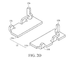
- FIG. 2D is a schematic view of a bent lead frame
- FIG. 3 is the process flow of manufacturing a magnetic device in FIG. 1A , FIG. 1E , FIG. 2C and FIG. 4A ;
- FIG. 4A is a schematic view of a magnetic device in the present invention, wherein the lead frame is formed by electroplating or etching;
- FIG. 4B is an exploded schematic view of the magnetic device shown in FIG. 4A .
- the present invention discloses a magnetic device in which a first portion and a second portion of a lead frame respectively are electrically connected with a first terminal and a second terminal of a coil through a first through opening and a second through opening of a core body to serve as a first electrode and a second electrode on the bottom of the magnetic device.
- FIG. 1A is a schematic view of a magnetic device 10 in the present invention.
- FIG. 1B is an exploded schematic view of the magnetic device 10 shown in FIG. 1A .
- FIG. 1C is a bottom schematic view of the magnetic device 10 shown in FIG. 1A .
- FIG 1 D is an exploded schematic view of the magnetic device 10 , wherein the first core body is a T-core body.
- FIG. 1E is a schematic view of the magnetic device 10 in the present invention, wherein the first core body is a T-core body.
- the magnetic device 10 includes a lead frame 11 , a first core body 12 , a coil 13 and a molding body 14 .
- the lead frame 11 has a first portion 11 a and a second portion 11 b spaced apart from the first portion 11 a .
- the first portion 11 a can comprise a first protrusion 15 a
- the second portion 11 b can comprise a second protrusion 15 b .
- the top of the first protrusion 15 a is higher than that of the first through opening 12 a
- the top of the second protrusion 15 b is higher than that of the second through opening 12 b .
- the first portion 11 a further comprises a third protrusion 15 c
- the second portion 11 b further comprises a fourth protrusion 15 d
- the first protrusion 15 a comprises a first foldable soldering pad 17 a
- the second protrusion 15 b comprises a second foldable soldering pad 17 b .
- the first portion 11 a of the lead frame 11 has a first foldable soldering pad 17 a folded to serve as the first protrusion 15 a
- the second portion 11 b of the lead frame 11 has a second foldable soldering pad 17 b folded to serve as the second protrusion 15 b
- the first protrusion 15 a comprises a first bent portion for connecting with a first terminal of a coil
- the second protrusion 15 b comprises a second bent portion for connecting with the second terminal of a coil.
- the first protrusion 15 a , the second protrusion 15 b , the third protrusion 15 c , the fourth protrusion 15 d can be formed by bending four segments of a flat lead frame 11 .
- the lead frame 11 can be also formed by electroplating or etching (described hereafter).
- a first core body 12 is disposed on the lead frame 11 .
- the first core body 12 is a magnetic core body.
- the first core body 12 can be made of any suitable magnetic powder, such as Fe alloy powder (Fe—Cr—Si, Fe—Al—Cr or Fe—Si—Al), ferrite powder (Ni—Zn ferrite or Mn—Zn ferrite), amorphous alloy powder or Fe powder.
- Fe alloy powder Fe—Cr—Si, Fe—Al—Cr or Fe—Si—Al
- ferrite powder Ni—Zn ferrite or Mn—Zn ferrite
- amorphous alloy powder or Fe powder e.g., Fe alloy powder, Fe—Cr—Si, Fe—Al—Cr or Fe—Si—Al
- ferrite powder Ni—Zn ferrite or Mn—Zn ferrite
- amorphous alloy powder or Fe powder e.g., Ni—Zn ferrite or Mn—Z
- the first core body 12 comprises a first through opening 12 a and a second through opening 12 b .
- first through opening 12 a and the second through opening 12 b are many different ways to locate the first through opening 12 a and the second through opening 12 b : in one embodiment, each of the first through opening 12 a and the second through opening 12 b is formed inside the first core body 12 ; in another embodiment, each of the first through opening 12 a and the second through opening 12 b is formed with one side of the opening aligned with one edge of the first core body 12 ; and in yet another embodiment, each of the first through opening 12 a and the second through opening 12 b is formed with two sides of the opening aligned with two edges of the first core body 12 respectively.
- a coil 13 is disposed on the first core body 12 .
- the coil 13 can be formed by wrapping round-wire, flat-wire or enameled-wire made of Cu or Ag.
- the coil 13 can be made of a conductive wire or a conductive pattern formed by any known technology, such as electroplating, etching, printing process or film process.
- the coil 13 has a first terminal 13 a and a second terminal 13 b .
- the first portion 11 a is electrically connected with the first terminal 13 a via the first through opening 12 a
- the second portion 15 b is electrically connected with the second terminal 13 b via the second through opening 12 b , respectively.
- the first portion ll a comprises a first protrusion 15 a and the second portion 11 b comprises a second protrusion 15 b , wherein the first protrusion 15 a is connected with the first terminal 13 a through the first through opening 12 a , and the second protrusion 15 b is connected with the second terminal 13 b through the second through opening 12 b , respectively.
- the top end of the first protrusion 15 a can be disposed in the first through opening 12 a
- the top end of the second protrusion 15 b can be disposed in the second through opening 12 b .
- the first joined point 16 a of the first terminal 13 a and the first protrusion 15 a can be inside the first through opening 12 a
- the second joined point 16 b of the second terminal 13 b and the second protrusion 15 b can be inside the second through opening 12 b
- at least one portion of the first protrusion 15 a is disposed outside the first through opening 12 a
- at least one portion of the second protrusion 15 b is disposed outside the second through opening 12 b .
- the first joined point 16 a of the first terminal 13 a and the first protrusion 15 a is substantially higher than the top of the first through opening 12 a
- the second joined point 16 b of the second terminal 13 b and the second protrusion 15 b is substantially higher than the top of the second through opening 12 b.
- a first conductive pillar (not shown) can be disposed in the first through opening 12 a to connect the first portion 11 a with the first terminal 13 a
- a second conductive pillar (not shown) can be disposed in the second through opening 12 b to connect the second portion 11 b with the second terminal 13 b , respectively. It has been disclosed in U.S. patent application Ser. No. 13/179,884, filed Jul. 11, 2011.
- the first core boy 12 has a first surface 12 c which is substantially flat, wherein the coil 13 is disposed on the first surface 12 c of the first core body 12 .
- the first core boy 12 e.g., T-core
- the first core boy 12 comprises a plate 12 e and a pillar 12 f having a top end and a bottom end, wherein the bottom end of the pillar 12 f is connected to the plate 12 e , wherein the coil 13 is disposed on the plate 12 e and winded around the pillar 12 f .
- the magnetic device 10 further comprises a second core body (not shown), wherein the coil 13 is disposed between the first core body 12 and the second core body.
- the material of the first core body 12 can be the same as that of the second core body or different from that of the second core body.
- the second core body is a magnetic core body.
- the second core body can be made of any suitable magnetic powder, such as Fe alloy powder (Fe—Cr—Si, Fe—Al—Cr or Fe—Si—Al), ferrite powder (Ni—Zn ferrite or Mn—Zn ferrite), amorphous alloy powder or Fe powder.
- Fe alloy powder Fe—Cr—Si, Fe—Al—Cr or Fe—Si—Al
- ferrite powder Ni—Zn ferrite or Mn—Zn ferrite
- a molding body 14 encapsulates the coil 13 .
- a first electrode is disposed on the bottom surface of the first portion 11 a and a second electrode is disposed on the bottom surface of the second portion 11 b . That is, the bottom of each of the first portion 11 a and the second portion 11 b of the lead frame 11 is exposed to the bottom of the molding body 14 such that the first portion 11 a and the second portion respectively 11 b serve as a first electrode and a second electrode of the magnetic device 10 .
- the first electrode and the second electrode of the magnetic device 10 can be formed by printing or electroplating.
- FIG. 3 is the process flow of manufacturing a magnetic device 10 , 20 , 30 in FIG. 1A , FIG. 1E , FIG. 2C and FIG. 4A .
- step 31 form a lead frame 11 having a first portion 11 a and a second portion 11 b spaced apart from the first portion 11 a .
- the first portion 11 a can comprise a first protrusion 15 a and the second portion 11 b can comprise a second protrusion 15 b.
- the lead frame can be formed by electroplating or etching.
- FIG. 4A is a schematic view of a magnetic device 30 in the present invention, wherein the lead frame 11 is formed by electroplating or etching.
- FIG. 4B is an exploded schematic view of the magnetic device 30 shown in FIG. 4A .
- Sn or Ni/Sn can be electroplated on a conductive material (e.g., copper foil) which can be made of Cu, or a conductive material (e.g., a metallic substrate) can be etched.
- a conductive material e.g., copper foil
- a conductive material e.g., a metallic substrate
- each of the first protrusion 15 a and the second protrusion 15 b is a conductive pillar.
- the magnetic device has a complete electrode plane, and the plane shape can be adjusted according to design demand. Compared to the lead frame formed by bending, the bottom electrodes of the magnetic device are complete, and adhesion area between the bottom electrodes of the magnetic device and the circuit board is maximized (utility rate of electrode area is larger than 90%) to enhance the adhesion strength. 2.
- the height and the shape of the protrusive conductive pillars can be adjusted to be adapted for various types of coils so that it is easier to weld and position the core body.
- the design of the bottom electrodes of the magnetic device can reduce the distance between devices on the circuit board. 4 .
- the lead frame can be directly adapted for SMD technology, so the electroplating steps in the process of the magnetic device can be saved and the material capable of be electroplated is not limited.
- step 32 dispose a first core body 12 on the lead frame 11 , wherein the first core body 12 comprises a first through opening 12 a and a second through opening 12 b .
- the magnetic device further comprises a second core body (not shown), wherein the coil is disposed between the first core body 12 and the second core body.
- the first core body 12 (or the second core body) is a magnetic core body.
- the material of the first core body 12 can be the same as that of the second core body or different from that of the second core body.
- the first core body 12 (or the second core body) can be formed by hot-pressing molding or cold-pressing molding, preferably, cold-pressing molding.
- step 33 dispose a coil 13 on the first core body 12 , wherein the coil 13 has a first terminal 13 a and a second terminal 13 b , wherein the first portion 11 a is electrically connected with the first terminal 13 a via the first through opening 12 a , and the second portion 11 b is electrically connected with the second terminal 13 b via the second through opening 12 b , respectively.
- the first portion 11 a comprises a first protrusion 15 a and the second portion 11 b comprises a second protrusion 15 b , wherein the first protrusion 15 a is connected with the first terminal 13 a through the first through opening 12 a , and the second protrusion 15 b is connected with the second terminal 13 b through the second through opening 12 b , respectively.
- a first conductive pillar (not shown) can be disposed in the first through opening 12 a to connect the first portion 11 a with the first terminal 13 a
- a second conductive pillar can be disposed in the second through opening 12 b to connect the second portion 11 b with the second terminal 13 b , respectively.
- the coil 13 can be formed by wrapping round-wire, flat-wire or enameled-wire made of Cu or Ag.
- the coil 13 can be made of a conductive wire or a conductive pattern formed by any known technology, such as electroplating, etching, printing process or film process.
- the molding body 14 can be formed by hot-pressing molding or cold-pressing molding, preferably, hot-pressing molding.
- a first electrode is disposed on the bottom surface of the first portion 11 a and a second electrode is disposed on the bottom surface of the second portion 11 b . That is, the bottom of each of the first portion 11 a and the second portion 11 b of the lead frame 11 is exposed to the bottom of the molding body 14 such that the first portion 11 a and the second portion 11 b respectively serve as a first electrode and a second electrode of the magnetic device.
- the first electrode and the second electrode of the magnetic device can be formed by printing or electroplating.
- a lead frame is formed by punching, electroplating or etching, and then the lead frame is dispensed.
- a core body is formed by cold-pressing molding and connected to the lead frame.
- the coil is disposed on the core body, and the terminals of the coil are electrically connected to the protrusions of the lead frame by spot welding or laser welding plus wire-head trimming.
- a molding body is formed to encapsulate the coil by hot-pressing molding and curing.
- the electrodes of the magnetic device are formed by electroplating or printing. Finally, the final product is done by trimming and passing electrical testing.
Abstract
A magnetic device comprises a lead frame, a first core body and a coil. The lead frame has a first portion and a second portion spaced apart from the first portion. A first core body is disposed on the lead frame, wherein the first core body comprises a first through opening and a second through opening. A coil is disposed on the first core body, wherein the coil has a first terminal and a second terminal, wherein the first portion is electrically connected with the first terminal via the first through opening, and the second portion is electrically connected with the second terminal via the second through opening, respectively.
Description
This application is a continuation of U.S. patent application Ser. No. 14/820,558, filed Aug. 7, 2015, which is a continuation of U.S. patent application Ser. No. 13/902,997, filed May 28, 2013, which claims the benefit of priority of U.S. Provisional Application No. 61/803,798, filed Mar. 21, 2013. All of these applications are incorporated by referenced herein in their entirety.
I. Field of the Invention
The present invention relates to a magnetic device and, in particular, to a magnetic device with electrodes made of a lead frame.
II. Description of the Prior Art
As an inductor has gradually become smaller and thinner, it is not easy to position the coil accurately which will affect product yield. The electrodes of the inductor are exposed to the lateral surface of the inductor so that a fixed space must be kept in the circuit board to prevent short circuit. Moreover, with the shrinkage of product size, a bad C-face crack will result from a bent stress when the electrodes of the inductor are bent during the molding process.
So far there are some drawbacks in the various types of inductors disclosed in the prior arts. In JP4795489B1, the design of the inductor which needs many electroplating steps induces a lot of process steps; the material capable of be electroplated is limited; and the electrodes of the inductor are exposed to the lateral surface of the inductor. In CN201207320Y, the conductive wires bent to the bottom of the iron core induce that the iron core doesn't have a smooth surface. If pressure is still applied in package process, the iron core easily has a crack.
Accordingly, the present invention proposes a magnetic device and a manufacturing method thereof to overcome the above-mentioned disadvantages.
One objective of the present invention is to provide a magnetic device with bottom electrodes made of a lead frame. The magnetic device comprises: a lead frame having a first portion and a second portion spaced apart from the first portion; a first core body disposed on the lead frame, wherein the first core body comprises a first through opening and a second through opening; and a coil disposed on the first core body, wherein the coil has a first terminal and a second terminal, wherein the first portion is electrically connected with the first terminal via the first through opening, and the second portion is electrically connected with the second terminal via the second through opening, respectively.
Preferably, the first portion comprises a first protrusion and the second portion comprises a second protrusion, wherein the first protrusion is connected with the first terminal through the first through opening, and the second protrusion is connected with the second terminal through the second through opening, respectively. A first conductive pillar can be disposed in the first through opening to connect the first portion with the first terminal, and a second conductive pillar can be disposed in the second through opening to connect the second portion with the second terminal, respectively.
A molding body encapsulates the coil. A first electrode is disposed on the bottom surface of the first portion and a second electrode is disposed on the bottom surface of the second portion. That is, the bottom of each of the first portion and the second portion of the lead frame is exposed to the bottom of the molding body such that the first portion and the second portion respectively serve as a first electrode and a second electrode of the magnetic device. The main advantages of the magnetic device in the present invention are described as follows: 1. Adhesion area between the bottom electrodes of the magnetic device and the circuit board is maximized to enhance the adhesion strength. 2. Because of no lateral electrode, product size can be shrunk and surface utility rate of the circuit board can be raised. 3. The height and the shape of the protrusions of the lead frame can be adjusted to be adapted for various types of coils so that it is easier to weld and position the core body. 4. The lead frame can be formed by various methods, such as folding, bending, electroplating or etching.
Another objective of the present invention is to provide a method for forming a magnetic device. The method comprises the steps of: forming a lead frame having a first portion and a second portion spaced apart from the first portion; disposing a first core body on the lead frame, wherein the first core body comprises a first through opening and a second through opening; and disposing a coil on the first core body, wherein the coil has a first terminal and a second terminal, wherein the first portion is electrically connected with the first terminal via the first through opening, and the second portion is electrically connected with the second terminal via the second through opening, respectively. In one embodiment of the magnetic device adapted for SMD technology, the lead frame can be formed by electroplating or etching.
Another objective of the present invention is to provide a method for forming a magnetic device, the method comprising the steps of: forming a lead frame comprising a first bottom part and a first protrusion connected to the first bottom part; forming a first core body, wherein the first core body comprises a first through opening; placing the first core body on the first bottom part of the lead frame, with at least a part of the first protrusion of the lead frame disposed in the first through opening for electrically connecting with a first terminal of a coil on the first core body; and encapsulating the first protrusion of the lead frame and the coil by using a molding material.
In one embodiment, the first bottom part and the first protrusion are integrally formed.
In one embodiment, the lead frame further comprises a second bottom part and a second protrusion connected to the second bottom part, and wherein the first core body further comprises a second through opening, wherein the first core body is placed on the first bottom part of the lead frame and at least a part of the second protrusion of the lead frame is disposed in the second through opening for electrically connecting with a second terminal of the coil on the first core body.
In one embodiment, the first bottom part and the first protrusion are integrally formed, and the second bottom part and the second protrusion are integrally formed.
In one embodiment, the lead frame is formed by electroplating a conductive pillar on a conductive material.
In one embodiment, the lead frame is formed by electroplating a conductive pillar on a copper foil.
In one embodiment, the lead frame is formed by etching a metallic substrate.
In one embodiment, the first protrusion comprises a first foldable soldering pad.
In one embodiment, the first protrusion comprises a first bent portion for connecting with the first terminal.
In one embodiment, the first through opening is formed with a first outer side surface of the first core body.
In one embodiment, the first through opening is formed with two outer side surfaces of the first core body.
In one embodiment, the first through opening is formed with a first outer side surface of the first core body; and the second through opening is formed with a second outer side surface of the first core body.
In one embodiment, the first through opening and the second through opening are respectively formed with two outer side surfaces of the first core body.
In one embodiment, the first through opening and the second through opening are respectively formed on a periphery of the first core body, wherein the first protrusion is not extended outside of any outer side surface of the first core body adjacent to the first through opening, and the second protrusion is not extended outside of any outer side surface of the first core body adjacent to the second through opening.
The detailed technology and above preferred embodiments implemented for the present invention are described in the following paragraphs accompanying the appended drawings for people skilled in this field to well appreciate the features of the claimed invention.
The foregoing aspects and many of the accompanying advantages of this invention will become more readily appreciated as the same becomes better understood by reference to the following detailed description when taken in conjunction with the accompanying drawings, wherein:
The detailed explanation of the present invention is described as following. The described preferred embodiments are presented for purposes of illustrations and description and they are not intended to limit the scope of the present invention.
The present invention discloses a magnetic device in which a first portion and a second portion of a lead frame respectively are electrically connected with a first terminal and a second terminal of a coil through a first through opening and a second through opening of a core body to serve as a first electrode and a second electrode on the bottom of the magnetic device.
The lead frame 11 has a first portion 11 a and a second portion 11 b spaced apart from the first portion 11 a. Optionally, the first portion 11 a can comprise a first protrusion 15 a, and the second portion 11 b can comprise a second protrusion 15 b. For a better electrical connection between the lead frame 11 and the coil 13, the top of the first protrusion 15 a is higher than that of the first through opening 12 a, and the top of the second protrusion 15 b is higher than that of the second through opening 12 b. Preferably, the first portion 11 a further comprises a third protrusion 15 c, and the second portion 11 b further comprises a fourth protrusion 15 d, wherein the first protrusion 15 a, the second protrusion 15 b, the third protrusion 15 c and the fourth protrusion 15 d surround the first core body 12. In one embodiment (see FIG. 2A , FIG. 2B and FIG. 2C ), the first protrusion 15 a comprises a first foldable soldering pad 17 a, and the second protrusion 15 b comprises a second foldable soldering pad 17 b. Specifically speaking, the first portion 11 a of the lead frame 11 has a first foldable soldering pad 17 a folded to serve as the first protrusion 15 a, and the second portion 11 b of the lead frame 11 has a second foldable soldering pad 17 b folded to serve as the second protrusion 15 b. In another embodiment (see FIG. 2D ), the first protrusion 15 a comprises a first bent portion for connecting with a first terminal of a coil, and the second protrusion 15 b comprises a second bent portion for connecting with the second terminal of a coil. For example, the first protrusion 15 a, the second protrusion 15 b, the third protrusion 15 c, the fourth protrusion 15 d can be formed by bending four segments of a flat lead frame 11. Moreover, the lead frame 11 can be also formed by electroplating or etching (described hereafter).
A first core body 12 is disposed on the lead frame 11. The first core body 12 is a magnetic core body. The first core body 12 can be made of any suitable magnetic powder, such as Fe alloy powder (Fe—Cr—Si, Fe—Al—Cr or Fe—Si—Al), ferrite powder (Ni—Zn ferrite or Mn—Zn ferrite), amorphous alloy powder or Fe powder. By pressing-molding process (e.g., heating or sintering), the magnetic powder and adhesive are mixed to form the first core body 12. The first core body 12 can have any suitable shape according design or practical application.
The first core body 12 comprises a first through opening 12 a and a second through opening 12 b. There are many different ways to locate the first through opening 12 a and the second through opening 12 b: in one embodiment, each of the first through opening 12 a and the second through opening 12 b is formed inside the first core body 12; in another embodiment, each of the first through opening 12 a and the second through opening 12 b is formed with one side of the opening aligned with one edge of the first core body 12; and in yet another embodiment, each of the first through opening 12 a and the second through opening 12 b is formed with two sides of the opening aligned with two edges of the first core body 12 respectively.
A coil 13 is disposed on the first core body 12. The coil 13 can be formed by wrapping round-wire, flat-wire or enameled-wire made of Cu or Ag. The coil 13 can be made of a conductive wire or a conductive pattern formed by any known technology, such as electroplating, etching, printing process or film process. The coil 13 has a first terminal 13 a and a second terminal 13 b. The first portion 11 a is electrically connected with the first terminal 13 a via the first through opening 12 a, and the second portion 15 b is electrically connected with the second terminal 13b via the second through opening 12 b, respectively. Preferably, the first portion llacomprises a first protrusion 15 a and the second portion 11 b comprises a second protrusion 15 b, wherein the first protrusion 15 a is connected with the first terminal 13 a through the first through opening 12 a, and the second protrusion 15 b is connected with the second terminal 13 b through the second through opening 12 b, respectively. In one embodiment, the top end of the first protrusion 15 a can be disposed in the first through opening 12 a, and the top end of the second protrusion 15 b can be disposed in the second through opening 12 b. In other words, refer to FIG. 1E and FIG. 4A , the first joined point 16 a of the first terminal 13 a and the first protrusion 15 a can be inside the first through opening 12 a, and the second joined point 16b of the second terminal 13 b and the second protrusion 15 b can be inside the second through opening 12 b. In another embodiment, at least one portion of the first protrusion 15 a is disposed outside the first through opening 12 a, and at least one portion of the second protrusion 15 b is disposed outside the second through opening 12 b. In other words, refer to FIG. 1A , the first joined point 16 a of the first terminal 13 a and the first protrusion 15 a is substantially higher than the top of the first through opening 12 a, and the second joined point 16 b of the second terminal 13 b and the second protrusion 15 b is substantially higher than the top of the second through opening 12 b.
A first conductive pillar (not shown) can be disposed in the first through opening 12 a to connect the first portion 11 a with the first terminal 13 a , and a second conductive pillar (not shown) can be disposed in the second through opening 12 b to connect the second portion 11 b with the second terminal 13 b, respectively. It has been disclosed in U.S. patent application Ser. No. 13/179,884, filed Jul. 11, 2011.
There are many different ways to dispose the coil 13 on the first core body 12. In one embodiment (see FIG. 1A and FIG. 1B ), the first core boy 12 has a first surface 12 c which is substantially flat, wherein the coil 13 is disposed on the first surface 12 c of the first core body 12. In another embodiment (see FIG. 1E , FIG. 2C and FIG. 4A ), the first core boy 12 (e.g., T-core) comprises a plate 12 e and a pillar 12 f having a top end and a bottom end, wherein the bottom end of the pillar 12 f is connected to the plate 12 e, wherein the coil 13 is disposed on the plate 12 e and winded around the pillar 12 f. In one embodiment, the magnetic device 10 further comprises a second core body (not shown), wherein the coil 13 is disposed between the first core body 12 and the second core body. The material of the first core body 12 can be the same as that of the second core body or different from that of the second core body.
The second core body is a magnetic core body. The second core body can be made of any suitable magnetic powder, such as Fe alloy powder (Fe—Cr—Si, Fe—Al—Cr or Fe—Si—Al), ferrite powder (Ni—Zn ferrite or Mn—Zn ferrite), amorphous alloy powder or Fe powder. By pressing-molding process (e.g., heating or sintering), the magnetic powder and adhesive are mixed to form the second core body. The second core body can have any suitable shape according design or practical application.
A molding body 14 encapsulates the coil 13. A first electrode is disposed on the bottom surface of the first portion 11 a and a second electrode is disposed on the bottom surface of the second portion 11 b. That is, the bottom of each of the first portion 11 a and the second portion 11 b of the lead frame 11 is exposed to the bottom of the molding body 14 such that the first portion 11 a and the second portion respectively 11 b serve as a first electrode and a second electrode of the magnetic device 10. The first electrode and the second electrode of the magnetic device 10 can be formed by printing or electroplating.
In step 31, form a lead frame 11 having a first portion 11 a and a second portion 11 b spaced apart from the first portion 11 a. Optionally, the first portion 11 a can comprise a first protrusion 15 a and the second portion 11 b can comprise a second protrusion 15 b.
In one embodiment of the magnetic device adapted for SMD technology, the lead frame can be formed by electroplating or etching. FIG. 4A is a schematic view of a magnetic device 30 in the present invention, wherein the lead frame 11 is formed by electroplating or etching. FIG. 4B is an exploded schematic view of the magnetic device 30 shown in FIG. 4A . To form the lead frame 11, for example, Sn or Ni/Sn can be electroplated on a conductive material (e.g., copper foil) which can be made of Cu, or a conductive material (e.g., a metallic substrate) can be etched. In this case, each of the first protrusion 15 a and the second protrusion 15 b is a conductive pillar. The advantages are listed as below: 1. The magnetic device has a complete electrode plane, and the plane shape can be adjusted according to design demand. Compared to the lead frame formed by bending, the bottom electrodes of the magnetic device are complete, and adhesion area between the bottom electrodes of the magnetic device and the circuit board is maximized (utility rate of electrode area is larger than 90%) to enhance the adhesion strength. 2. The height and the shape of the protrusive conductive pillars can be adjusted to be adapted for various types of coils so that it is easier to weld and position the core body. 3. The design of the bottom electrodes of the magnetic device can reduce the distance between devices on the circuit board. 4. The lead frame can be directly adapted for SMD technology, so the electroplating steps in the process of the magnetic device can be saved and the material capable of be electroplated is not limited.
In step 32, dispose a first core body 12 on the lead frame 11, wherein the first core body 12 comprises a first through opening 12 a and a second through opening 12 b. In one embodiment, the magnetic device further comprises a second core body (not shown), wherein the coil is disposed between the first core body 12 and the second core body. The first core body 12 (or the second core body) is a magnetic core body. The material of the first core body 12 can be the same as that of the second core body or different from that of the second core body. The first core body 12 (or the second core body) can be formed by hot-pressing molding or cold-pressing molding, preferably, cold-pressing molding.
In step 33, dispose a coil 13 on the first core body 12, wherein the coil 13 has a first terminal 13 a and a second terminal 13 b, wherein the first portion 11 a is electrically connected with the first terminal 13 a via the first through opening 12 a, and the second portion 11 b is electrically connected with the second terminal 13b via the second through opening 12 b, respectively. Preferably, the first portion 11 a comprises a first protrusion 15 a and the second portion 11 b comprises a second protrusion 15 b , wherein the first protrusion 15 a is connected with the first terminal 13 a through the first through opening 12 a, and the second protrusion 15 b is connected with the second terminal 13 b through the second through opening 12 b, respectively. A first conductive pillar (not shown) can be disposed in the first through opening 12 a to connect the first portion 11 a with the first terminal 13 a , and a second conductive pillar (not shown) can be disposed in the second through opening 12 b to connect the second portion 11 b with the second terminal 13 b, respectively. The coil 13 can be formed by wrapping round-wire, flat-wire or enameled-wire made of Cu or Ag. The coil 13 can be made of a conductive wire or a conductive pattern formed by any known technology, such as electroplating, etching, printing process or film process.
In step 34, form a molding body 14 to encapsulate the coil 13. The molding body 14 can be formed by hot-pressing molding or cold-pressing molding, preferably, hot-pressing molding. A first electrode is disposed on the bottom surface of the first portion 11 a and a second electrode is disposed on the bottom surface of the second portion 11 b. That is, the bottom of each of the first portion 11 a and the second portion 11 b of the lead frame 11 is exposed to the bottom of the molding body 14 such that the first portion 11 a and the second portion 11 b respectively serve as a first electrode and a second electrode of the magnetic device. The first electrode and the second electrode of the magnetic device can be formed by printing or electroplating.
Detailed process is listed as below. A lead frame is formed by punching, electroplating or etching, and then the lead frame is dispensed. A core body is formed by cold-pressing molding and connected to the lead frame. The coil is disposed on the core body, and the terminals of the coil are electrically connected to the protrusions of the lead frame by spot welding or laser welding plus wire-head trimming. A molding body is formed to encapsulate the coil by hot-pressing molding and curing. The electrodes of the magnetic device are formed by electroplating or printing. Finally, the final product is done by trimming and passing electrical testing.
The above disclosure is related to the detailed technical contents and inventive features thereof. People skilled in this field may proceed with a variety of modifications and replacements based on the disclosures and suggestions of the invention as described without departing from the characteristics thereof. Nevertheless, although such modifications and replacements are not fully disclosed in the above descriptions, they have substantially been covered in the following claims as appended.
Claims (20)
1. An inductor, comprising:
a magnetic body, wherein a first through opening is formed on a periphery of the magnetic body; and
a first lead comprising a first conductive part and a second conductive part electrically connected to the first conductive part, wherein the first conductive part is disposed on the bottom surface of the magnetic body and a bottom surface of the first conductive part is located under said first through opening, and at least a portion of the second conductive part is disposed in the first through opening, wherein a conductive path is formed from a first terminal of a coil of the inductor to the first conductive part via the second conductive part.
2. The inductor according to claim 1 , wherein there is no other conductive part that is located outside of any outer side surface of the magnetic body adjacent to the first through opening and used for soldering with the first terminal of the coil.
3. The inductor according to claim 1 , wherein the first conductive part and the second conductive part of the first lead are integrally formed by metallic material, wherein the bottom surface of the first conductive part is substantially flat.
4. The inductor according to claim 1 , wherein the first through opening is formed by at least two outer side surfaces of the periphery of the magnetic body, wherein said two outer side surfaces are substantially perpendicular to each other.
5. The inductor according to claim 1 , wherein a second through opening is formed on a periphery of the magnetic body, further comprising a second lead comprising a third conductive part and a fourth conductive part connected to the third conductive part, wherein the third conductive part is disposed on the bottom surface of the magnetic body a bottom surface of the second conductive part is located under said second through opening, and at least a portion of the fourth conductive part is disposed in the second through opening and electrically connected to a second terminal of the coil.
6. The inductor according to claim 5 , wherein the second through opening is formed by at least two outer side surfaces of the magnetic body, wherein said two outer surfaces are substantially perpendicular to each other.
7. The inductor according to claim 1 , wherein the top end of the second conductive part is disposed in the first through opening.
8. An inductor, comprising:
a magnetic core, comprising a first through opening;
a coil disposed on the magnetic body;
a first lead comprising a first conductive part and a second conductive part electrically connected to the first conductive part, wherein the first conductive part is disposed on the bottom surface of the magnetic body and a bottom surface of the first conductive part is located under said first through opening, and at least a portion of the second conductive part is disposed in the first through opening, wherein a conductive path is formed from a first terminal of a coil to the first conductive part via the second conductive part; and
a molding body, wherein the coil and the second conductive part are encapsulated by the molding body.
9. The inductor according to claim 8 , wherein the first conductive part and the second conductive part are integrally formed by metallic material, wherein the bottom surface of the first conductive part is substantially flat.
10. The inductor according to claim 8 , wherein the molding body encapsulates the magnetic core, the coil and the second conductive part.
11. The inductor according to claim 8 , wherein the magnetic core further comprises a second through opening, further comprising a second lead comprising a third conductive part and a fourth conductive part connected to the third conductive part, wherein the third conductive part is disposed on the bottom surface of the magnetic body and a bottom surface of the third conductive part is located under said second through hole, and at least a portion of the fourth conductive part is disposed in the second through opening and electrically connected to a second terminal of the coil.
12. The inductor according to claim 8 , wherein the first through opening is formed on a first corner of the periphery of the magnetic body.
13. The inductor according to claim 11 , wherein the second through opening is formed on a second corner of the periphery of the magnetic body.
14. The inductor according to claim 8 , wherein the top end of the second conductive part is disposed in the first through opening.
15. The inductor device according to claim 11 , wherein the top end of the fourth conductive part is disposed in the first through opening.
16. An inductor, comprising:
a magnetic body, wherein a first through opening is formed on a periphery of the magnetic body; and
a first lead comprising a first conductive part and a second conductive part connected to the first conductive part, wherein the first conductive part is disposed on the bottom surface of the magnetic body and a bottom surface of the first conductive part is located under said first through opening, and at least a portion of the second conductive part is disposed in the first through opening, wherein a conductive path is formed from a first terminal of a coil of the inductor to the first conductive part via the second conductive part, wherein the first through opening is formed by at least two outer side surfaces of the periphery of the magnetic body, wherein said two outer side surfaces are substantially perpendicular to each other.
17. The inductor according to claim 16 , wherein the first conductive part and the second conductive part are integrally formed by metallic material, wherein the bottom surface of the first conductive part is substantially flat.
18. The inductor according to claim 16 , wherein a second through opening is formed on the periphery of the magnetic body, further comprising a second lead comprising a third conductive part and a fourth conductive part connected to the third conductive part, wherein the third conductive part is disposed on the bottom surface of the magnetic body and a bottom surface of the third conductive part is located under said second through opening, and at least a portion of the fourth conductive part is disposed in the second through hole and electrically connected to a second terminal of the coil.
19. The inductor according to claim 16 , wherein the first through opening is formed on a first corner of the periphery of the magnetic body.
20. The inductor according to claim 18 , wherein the second through opening is formed on a second corner of the periphery of the magnetic body.
Priority Applications (1)
| Application Number | Priority Date | Filing Date | Title |
|---|---|---|---|
| US15/409,549 US9805860B2 (en) | 2013-03-21 | 2017-01-19 | Magnetic device and method of manufacturing the same |
Applications Claiming Priority (4)
| Application Number | Priority Date | Filing Date | Title |
|---|---|---|---|
| US201361803798P | 2013-03-21 | 2013-03-21 | |
| US13/902,997 US9136050B2 (en) | 2010-07-23 | 2013-05-28 | Magnetic device and method of manufacturing the same |
| US14/820,558 US9576710B2 (en) | 2013-03-21 | 2015-08-07 | Magnetic device and method of manufacturing the same |
| US15/409,549 US9805860B2 (en) | 2013-03-21 | 2017-01-19 | Magnetic device and method of manufacturing the same |
Related Parent Applications (1)
| Application Number | Title | Priority Date | Filing Date |
|---|---|---|---|
| US14/820,558 Continuation US9576710B2 (en) | 2013-03-21 | 2015-08-07 | Magnetic device and method of manufacturing the same |
Publications (2)
| Publication Number | Publication Date |
|---|---|
| US20170133149A1 US20170133149A1 (en) | 2017-05-11 |
| US9805860B2 true US9805860B2 (en) | 2017-10-31 |
Family
ID=51551988
Family Applications (3)
| Application Number | Title | Priority Date | Filing Date |
|---|---|---|---|
| US13/902,997 Active 2031-07-28 US9136050B2 (en) | 2010-07-23 | 2013-05-28 | Magnetic device and method of manufacturing the same |
| US14/820,558 Active 2033-06-02 US9576710B2 (en) | 2013-03-21 | 2015-08-07 | Magnetic device and method of manufacturing the same |
| US15/409,549 Active US9805860B2 (en) | 2013-03-21 | 2017-01-19 | Magnetic device and method of manufacturing the same |
Family Applications Before (2)
| Application Number | Title | Priority Date | Filing Date |
|---|---|---|---|
| US13/902,997 Active 2031-07-28 US9136050B2 (en) | 2010-07-23 | 2013-05-28 | Magnetic device and method of manufacturing the same |
| US14/820,558 Active 2033-06-02 US9576710B2 (en) | 2013-03-21 | 2015-08-07 | Magnetic device and method of manufacturing the same |
Country Status (3)
| Country | Link |
|---|---|
| US (3) | US9136050B2 (en) |
| CN (2) | CN106449014B (en) |
| TW (2) | TWI508111B (en) |
Cited By (1)
| Publication number | Priority date | Publication date | Assignee | Title |
|---|---|---|---|---|
| USD980069S1 (en) | 2020-07-14 | 2023-03-07 | Ball Corporation | Metallic dispensing lid |
Families Citing this family (34)
| Publication number | Priority date | Publication date | Assignee | Title |
|---|---|---|---|---|
| US20080036566A1 (en) | 2006-08-09 | 2008-02-14 | Andrzej Klesyk | Electronic Component And Methods Relating To Same |
| US9087634B2 (en) | 2013-03-14 | 2015-07-21 | Sumida Corporation | Method for manufacturing electronic component with coil |
| US9576721B2 (en) * | 2013-03-14 | 2017-02-21 | Sumida Corporation | Electronic component and method for manufacturing electronic component |
| CN103915236A (en) * | 2014-04-01 | 2014-07-09 | 黄伟嫦 | Novel inductor and manufacturing method thereof |
| US9831023B2 (en) * | 2014-07-10 | 2017-11-28 | Cyntec Co., Ltd. | Electrode structure and the corresponding electrical component using the same and the fabrication method thereof |
| CN105469976B (en) | 2014-09-11 | 2019-04-05 | 胜美达集团株式会社 | The manufacturing method and coil part of coil part |
| US10049808B2 (en) * | 2014-10-31 | 2018-08-14 | Samsung Electro-Mechanics Co., Ltd. | Coil component assembly for mass production of coil components and coil components made from coil component assembly |
| US10170234B2 (en) * | 2015-01-22 | 2019-01-01 | Tdk Corporation | Coil device capable of performing a wire connection |
| JP2016157751A (en) | 2015-02-23 | 2016-09-01 | スミダコーポレーション株式会社 | Electronic component |
| US20180218826A1 (en) * | 2015-07-10 | 2018-08-02 | James MILLSAP | Magnetic core, and choke or transformer having such a magnetic core |
| US9899131B2 (en) * | 2015-07-20 | 2018-02-20 | Cyntec Co., Ltd. | Structure of an electronic component and an inductor |
| KR101719916B1 (en) * | 2015-08-18 | 2017-03-24 | 삼성전기주식회사 | Coil electronic part |
| US10210992B2 (en) | 2015-10-06 | 2019-02-19 | Cyntec Co., Ltd. | Apparatus of coupled inductors with balanced electromotive forces |
| JP6759609B2 (en) * | 2016-02-04 | 2020-09-23 | Tdk株式会社 | Coil parts |
| JP6728730B2 (en) * | 2016-02-04 | 2020-07-22 | Tdk株式会社 | Coil parts |
| US10643784B2 (en) * | 2016-04-20 | 2020-05-05 | Bel Fuse (Macao Commercial Offshore) Limited | Filter inductor for heavy-current application |
| US10446309B2 (en) | 2016-04-20 | 2019-10-15 | Vishay Dale Electronics, Llc | Shielded inductor and method of manufacturing |
| JP6597576B2 (en) * | 2016-12-08 | 2019-10-30 | 株式会社村田製作所 | Inductor and DC-DC converter |
| JP6822129B2 (en) * | 2016-12-21 | 2021-01-27 | 株式会社村田製作所 | Surface mount inductor |
| CN108335821B (en) * | 2017-01-20 | 2020-06-26 | 乾坤科技股份有限公司 | Coil component |
| KR102369430B1 (en) * | 2017-03-15 | 2022-03-03 | 삼성전기주식회사 | Coil electronic component and board having the same |
| JP2018182209A (en) * | 2017-04-19 | 2018-11-15 | 株式会社村田製作所 | Coil component |
| JP7052238B2 (en) * | 2017-07-18 | 2022-04-12 | Tdk株式会社 | Coil device |
| CN109390137A (en) * | 2017-08-03 | 2019-02-26 | 联振电子(深圳)有限公司 | The electrode slice and its manufacturing method of inductance |
| KR102501904B1 (en) * | 2017-12-07 | 2023-02-21 | 삼성전기주식회사 | Winding type inductor |
| JP7148245B2 (en) * | 2018-01-26 | 2022-10-05 | 太陽誘電株式会社 | Wound coil parts |
| JP7148247B2 (en) * | 2018-02-09 | 2022-10-05 | 太陽誘電株式会社 | Coil parts and electronic equipment |
| CN110381715B (en) * | 2018-04-13 | 2022-05-06 | 乾坤科技股份有限公司 | Shielding magnetic device |
| JP2020077790A (en) * | 2018-11-08 | 2020-05-21 | 株式会社村田製作所 | Surface mount inductor |
| JP2020077795A (en) * | 2018-11-08 | 2020-05-21 | 株式会社村田製作所 | Surface mount inductor |
| CN109754987B (en) * | 2019-02-13 | 2021-01-26 | 青岛云路新能源科技有限公司 | Integrated into one piece inductor |
| KR102189800B1 (en) * | 2019-03-18 | 2020-12-11 | 삼성전기주식회사 | Coil component |
| US11855540B2 (en) * | 2019-03-26 | 2023-12-26 | Texas Instruments Incorporated | Leadframe for conductive winding |
| JP2021027201A (en) * | 2019-08-06 | 2021-02-22 | 株式会社村田製作所 | Inductor |
Citations (2)
| Publication number | Priority date | Publication date | Assignee | Title |
|---|---|---|---|---|
| US5912609A (en) * | 1996-07-01 | 1999-06-15 | Tdk Corporation | Pot-core components for planar mounting |
| US6621397B2 (en) * | 2000-08-14 | 2003-09-16 | Delta Electronics Inc. | Low profile inductor |
Family Cites Families (23)
| Publication number | Priority date | Publication date | Assignee | Title |
|---|---|---|---|---|
| US3551864A (en) * | 1969-12-12 | 1970-12-29 | Pico Electronics Inc | Miniature inductive devices |
| JPS5926577Y2 (en) * | 1979-09-17 | 1984-08-02 | ティーディーケイ株式会社 | small inductance element |
| JPS57170519U (en) * | 1981-04-20 | 1982-10-27 | ||
| US4553123A (en) * | 1982-09-03 | 1985-11-12 | Murata Manufacturing Co., Ltd. | Miniature inductor |
| JPS625618A (en) * | 1985-07-02 | 1987-01-12 | Matsushita Electric Ind Co Ltd | Chip inductor |
| JPH07335449A (en) * | 1994-06-13 | 1995-12-22 | Hitachi Ferrite Ltd | Coil part |
| GB2296387B (en) * | 1994-12-02 | 1999-10-13 | Dale Electronics | Low profile inductor/transformer component |
| JP3411758B2 (en) * | 1996-08-09 | 2003-06-03 | 太陽誘電株式会社 | Surface mount inductor |
| JP2004207371A (en) * | 2002-12-24 | 2004-07-22 | Tokyo Coil Engineering Kk | Surface mounting choke coil |
| TW200428426A (en) * | 2003-06-11 | 2004-12-16 | de-lu Ceng | Thin inductor and manufacturing method thereof |
| JP4315425B2 (en) * | 2003-07-23 | 2009-08-19 | スミダコーポレーション株式会社 | Ultra-small surface mount coil device |
| JP2005142459A (en) * | 2003-11-10 | 2005-06-02 | Toko Inc | Surface mounted inductor |
| JP2006041418A (en) * | 2004-07-30 | 2006-02-09 | Toko Inc | Plate-mounting coil component |
| KR20070066561A (en) * | 2005-12-22 | 2007-06-27 | 삼성전자주식회사 | Inductor apparatus, circuit board, and electronic device using the same |
| US20080036566A1 (en) * | 2006-08-09 | 2008-02-14 | Andrzej Klesyk | Electronic Component And Methods Relating To Same |
| KR101147019B1 (en) * | 2007-09-10 | 2012-05-17 | 스미다 코포레이션 가부시키가이샤 | Magnetic component |
| JP2010093063A (en) * | 2008-10-08 | 2010-04-22 | Tdk Corp | Metal powder compacting coil component |
| JP5161136B2 (en) * | 2009-02-27 | 2013-03-13 | スミダコーポレーション株式会社 | Inductor and method of manufacturing inductor |
| TW201036011A (en) * | 2009-03-20 | 2010-10-01 | Delta Electronics Inc | Surface mount magnetic device, the winding thereof, and the method for fabricating the same |
| JP5167382B2 (en) * | 2010-04-27 | 2013-03-21 | スミダコーポレーション株式会社 | Coil parts |
| TWI438792B (en) * | 2011-01-04 | 2014-05-21 | Cyntec Co Ltd | Inductor |
| CN102903492B (en) * | 2011-07-25 | 2015-08-26 | 胜美达集团株式会社 | Magnetic element |
| TWM426149U (en) * | 2011-09-23 | 2012-04-01 | Yujing Technology Co Ltd | Ultra thin filter structure |
-
2013
- 2013-05-28 US US13/902,997 patent/US9136050B2/en active Active
-
2014
- 2014-03-20 TW TW103110571A patent/TWI508111B/en active
- 2014-03-20 TW TW104132684A patent/TWI578341B/en active
- 2014-03-20 CN CN201610939977.9A patent/CN106449014B/en active Active
- 2014-03-20 CN CN201410105852.7A patent/CN104064319B/en active Active
-
2015
- 2015-08-07 US US14/820,558 patent/US9576710B2/en active Active
-
2017
- 2017-01-19 US US15/409,549 patent/US9805860B2/en active Active
Patent Citations (2)
| Publication number | Priority date | Publication date | Assignee | Title |
|---|---|---|---|---|
| US5912609A (en) * | 1996-07-01 | 1999-06-15 | Tdk Corporation | Pot-core components for planar mounting |
| US6621397B2 (en) * | 2000-08-14 | 2003-09-16 | Delta Electronics Inc. | Low profile inductor |
Cited By (1)
| Publication number | Priority date | Publication date | Assignee | Title |
|---|---|---|---|---|
| USD980069S1 (en) | 2020-07-14 | 2023-03-07 | Ball Corporation | Metallic dispensing lid |
Also Published As
| Publication number | Publication date |
|---|---|
| US20170133149A1 (en) | 2017-05-11 |
| CN106449014B (en) | 2019-11-15 |
| TWI578341B (en) | 2017-04-11 |
| TWI508111B (en) | 2015-11-11 |
| CN104064319B (en) | 2017-01-11 |
| CN106449014A (en) | 2017-02-22 |
| TW201440095A (en) | 2014-10-16 |
| US20150348707A1 (en) | 2015-12-03 |
| US9136050B2 (en) | 2015-09-15 |
| CN104064319A (en) | 2014-09-24 |
| US20140002227A1 (en) | 2014-01-02 |
| TW201603069A (en) | 2016-01-16 |
| US9576710B2 (en) | 2017-02-21 |
Similar Documents
| Publication | Publication Date | Title |
|---|---|---|
| US9805860B2 (en) | Magnetic device and method of manufacturing the same | |
| US11869696B2 (en) | Electronic component | |
| US10796842B2 (en) | Method to form an inductive component | |
| US8695209B2 (en) | Method of producing a surface-mount inductor | |
| US8183967B2 (en) | Surface mount magnetic components and methods of manufacturing the same | |
| US8188824B2 (en) | Surface mount magnetic components and methods of manufacturing the same | |
| US20130307655A1 (en) | Surface Mount Inductor and Method for Producing Surface Mount Inductor | |
| CN102290208B (en) | Coil-embedded dust magnetic core and its manufacturing method | |
| WO2015045955A1 (en) | Wound electronic component and method for manufacturing wound electronic component | |
| WO2020164645A2 (en) | Inductive component and manufacturing method | |
| CN205542250U (en) | Inductor structure | |
| KR20160134633A (en) | Wire wound inductor and manufacturing method thereof | |
| JP6927115B2 (en) | Surface mount inductor and its manufacturing method | |
| KR102558332B1 (en) | Inductor and producing method of the same | |
| CN105575644A (en) | Fabrication method for inductor free of welding point | |
| KR20170014598A (en) | Coil electronic component and method for manufacturing same | |
| KR101111999B1 (en) | Power inductor and method for manufacturing the same | |
| JP6086113B2 (en) | Surface mount inductor and manufacturing method thereof | |
| US20210193374A1 (en) | Coil device | |
| CN112466632A (en) | Element with inductance and method for forming inductor | |
| JP2004207355A (en) | Surface-mounting electronic component and method of manufacturing same |
Legal Events
| Date | Code | Title | Description |
|---|---|---|---|
| AS | Assignment |
Owner name: CYNTEC CO., LTD., TAIWAN Free format text: ASSIGNMENT OF ASSIGNORS INTEREST;ASSIGNORS:HSIEH, ROGER;LEE, CHENG-CHANG;LIU, CHUN-TIAO;AND OTHERS;REEL/FRAME:041256/0935 Effective date: 20170126 |
|
| STCF | Information on status: patent grant |
Free format text: PATENTED CASE |
|
| MAFP | Maintenance fee payment |
Free format text: PAYMENT OF MAINTENANCE FEE, 4TH YEAR, LARGE ENTITY (ORIGINAL EVENT CODE: M1551); ENTITY STATUS OF PATENT OWNER: LARGE ENTITY Year of fee payment: 4 |