US9804471B2 - Passive matrix display device and method of making the same - Google Patents
Passive matrix display device and method of making the same Download PDFInfo
- Publication number
- US9804471B2 US9804471B2 US14/804,222 US201514804222A US9804471B2 US 9804471 B2 US9804471 B2 US 9804471B2 US 201514804222 A US201514804222 A US 201514804222A US 9804471 B2 US9804471 B2 US 9804471B2
- Authority
- US
- United States
- Prior art keywords
- conductive lines
- electrodes
- display device
- conductive
- passive matrix
- Prior art date
- Legal status (The legal status is an assumption and is not a legal conclusion. Google has not performed a legal analysis and makes no representation as to the accuracy of the status listed.)
- Expired - Fee Related, expires
Links
Images


Classifications
-
- G—PHYSICS
- G02—OPTICS
- G02F—OPTICAL DEVICES OR ARRANGEMENTS FOR THE CONTROL OF LIGHT BY MODIFICATION OF THE OPTICAL PROPERTIES OF THE MEDIA OF THE ELEMENTS INVOLVED THEREIN; NON-LINEAR OPTICS; FREQUENCY-CHANGING OF LIGHT; OPTICAL LOGIC ELEMENTS; OPTICAL ANALOGUE/DIGITAL CONVERTERS
- G02F1/00—Devices or arrangements for the control of the intensity, colour, phase, polarisation or direction of light arriving from an independent light source, e.g. switching, gating or modulating; Non-linear optics
- G02F1/01—Devices or arrangements for the control of the intensity, colour, phase, polarisation or direction of light arriving from an independent light source, e.g. switching, gating or modulating; Non-linear optics for the control of the intensity, phase, polarisation or colour
- G02F1/165—Devices or arrangements for the control of the intensity, colour, phase, polarisation or direction of light arriving from an independent light source, e.g. switching, gating or modulating; Non-linear optics for the control of the intensity, phase, polarisation or colour based on translational movement of particles in a fluid under the influence of an applied field
- G02F1/166—Devices or arrangements for the control of the intensity, colour, phase, polarisation or direction of light arriving from an independent light source, e.g. switching, gating or modulating; Non-linear optics for the control of the intensity, phase, polarisation or colour based on translational movement of particles in a fluid under the influence of an applied field characterised by the electro-optical or magneto-optical effect
- G02F1/167—Devices or arrangements for the control of the intensity, colour, phase, polarisation or direction of light arriving from an independent light source, e.g. switching, gating or modulating; Non-linear optics for the control of the intensity, phase, polarisation or colour based on translational movement of particles in a fluid under the influence of an applied field characterised by the electro-optical or magneto-optical effect by electrophoresis
-
- G—PHYSICS
- G02—OPTICS
- G02F—OPTICAL DEVICES OR ARRANGEMENTS FOR THE CONTROL OF LIGHT BY MODIFICATION OF THE OPTICAL PROPERTIES OF THE MEDIA OF THE ELEMENTS INVOLVED THEREIN; NON-LINEAR OPTICS; FREQUENCY-CHANGING OF LIGHT; OPTICAL LOGIC ELEMENTS; OPTICAL ANALOGUE/DIGITAL CONVERTERS
- G02F1/00—Devices or arrangements for the control of the intensity, colour, phase, polarisation or direction of light arriving from an independent light source, e.g. switching, gating or modulating; Non-linear optics
- G02F1/01—Devices or arrangements for the control of the intensity, colour, phase, polarisation or direction of light arriving from an independent light source, e.g. switching, gating or modulating; Non-linear optics for the control of the intensity, phase, polarisation or colour
- G02F1/13—Devices or arrangements for the control of the intensity, colour, phase, polarisation or direction of light arriving from an independent light source, e.g. switching, gating or modulating; Non-linear optics for the control of the intensity, phase, polarisation or colour based on liquid crystals, e.g. single liquid crystal display cells
- G02F1/133—Constructional arrangements; Operation of liquid crystal cells; Circuit arrangements
- G02F1/1333—Constructional arrangements; Manufacturing methods
- G02F1/1343—Electrodes
- G02F1/134309—Electrodes characterised by their geometrical arrangement
- G02F1/134336—Matrix
Definitions
- Embodiments of the present invention relate to a passive matrix display device and a method of making the same.
- display devices have been increasingly used as, for example, an output and/or a user interface for electronic devices, such as mobile phones, televisions, electronic watches, and other various personal electronic devices.
- Manufacturing such displays including liquid crystal displays (LCDs), organic light emitting diode (OLED) displays, and the like, is relatively expensive.
- LCDs liquid crystal displays
- OLED organic light emitting diode
- a process including various specialized tooling and a carefully controlled environment may be used to manufacture the display devices.
- the specialized tooling may only be suitable to manufacture a display device having a certain size, and other tooling may be necessary to manufacture a display device having a different size.
- prototype display devices are relatively expensive as specialized tooling may need to be manufactured or used to manufacture even a single prototype display.
- the relatively high cost of manufacturing prototype display devices means that hobbyists and the like cannot easily manufacture display devices for a specific application or project.
- aspects of embodiments of the present invention include a passive matrix display device and a method of making the passive matrix display device.
- a passive matrix display device includes: a first electrode panel including a first substrate, a plurality of anisotropic conductive lines on the first substrate extending in a first direction, and a plurality of first electrodes, each of the first electrodes including some of the plurality of anisotropic conductive lines, and others of the plurality of anisotropic conductive lines being arranged between and contacting both adjacent ones of the first electrodes; a second electrode panel including a second substrate, a plurality of anisotropic conductive lines on the second substrate extending in a second direction crossing the first direction, and a plurality of second electrodes, each of the second electrodes including some of the plurality of anisotropic conductive lines, and others of the plurality of anisotropic conductive lines being arranged between and contacting both adjacent ones of the second electrodes; and a display control medium between the first electrode panel and the second electrode panel and configured to be varied by an electric field generated between the first electrodes and the second electrodes.
- the anisotropic conductive lines may include carbon nanotubes.
- the display control medium may include an electronic ink sheet.
- the first electrode panel may further include a plurality of conductive traces at a first end of the anisotropic conductive lines and defining the first electrodes.
- At least one of the plurality of conductive traces may have a different length than at least another one of the plurality of conductive traces.
- the first electrode panel may further include another plurality of conductive traces at a second end of the anisotropic conductive lines.
- Ones of the plurality of conductive traces may be aligned with corresponding ones of the other plurality of conductive traces.
- the first electrode panel may further include a plurality of conductive lines and another plurality of conductive lines.
- Ones of the conductive lines may be connected to respective ones of the plurality of conductive traces, and ones of the other plurality of conductive lines may be connected to respective ones of the other plurality of conductive traces.
- Each of the other plurality of conductive lines may extend along one side of the plurality of anisotropic conductive lines.
- Some of the other plurality of conductive lines may extend along one side of the plurality of anisotropic conductive lines, and others of the other plurality of conductive lines may extend along an opposite side of the plurality of anisotropic conductive lines.
- a method of making a passive matrix display device includes: placing a plurality of anisotropic conductive lines on a first substrate extending in a first direction, the plurality of anisotropic conductive lines forming a continuous layer; placing a plurality of anisotropic conductive lines on a second substrate extending in a second direction crossing the first direction, the plurality of anisotropic conductive lines forming a continuous layer; and arranging a display control medium between the first substrate and the second substrate.
- the providing the plurality of anisotropic conductive lines may include moving the first substrate with respect to a carbon nanotube ingot in the first direction, while the first substrate is in contact with the carbon nanotube ingot.
- the method may further include forming a plurality of conductive traces at a first end of the anisotropic conductive lines to define a corresponding plurality of first electrodes, adjacent ones of the plurality of conductive traces being spaced from each other.
- Some of the plurality of anisotropic conductive lines may be arranged between and may contact both adjacent ones of the plurality of first electrodes.
- At least one of the plurality of conductive traces may have a length different from at least another one of the plurality of conductive traces.
- the method may further include removing a portion of each of the first substrate, the second substrate, and the display control medium.
- the passive matrix display device After the removing the portion of each of the first substrate, the second substrate, and the display control medium, the passive matrix display device may have a non-quadrangular shape.
- a passive matrix display device includes a first electrode panel, a second electrode panel, and a display control medium
- a method of making the passive matrix display device includes: forming a plurality of conductive traces on a first electrode panel, each of the plurality of conductive traces extending across a plurality of anisotropic conductive lines on the first electrode panel; forming a plurality of conductive traces on a second electrode panel, each of the plurality of conductive traces extending across a plurality of anisotropic conductive lines on the second electrode panel; and arranging a display control medium between the first electrode panel and the second electrode panel.
- At least one of the plurality of conductive traces may have a length that is different from another one of the plurality of conductive traces.
- the method may further include removing a portion of the first electrode panel, the second electrode panel, and the display control medium such that the passive matrix display device has a non-quadrangular shape.
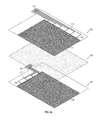
- FIG. 1 illustrates a display device according to an embodiment of the present invention
- FIG. 2 illustrates a first electrode panel of the display device according to an embodiment of the present invention
- FIG. 3 illustrates a second electrode panel of the display device according to an embodiment of the present invention
- FIG. 4 illustrates an assembled display panel according to an embodiment of the present invention
- FIG. 5 illustrates a second electrode panel of the display device according to an embodiment of the present invention
- FIG. 6 illustrates an assembled display panel according to an embodiment of the present invention
- FIG. 7 illustrates an assembled display panel and a controller according to an embodiment of the present invention.
- FIGS. 8 a -8 g illustrate a method of making a passive matrix display device according to an embodiment of the present invention.
- spatially relative terms such as “beneath,” “below,” “lower,” “under,” “above,” “upper,” and the like, may be used herein for ease of explanation to describe one element or feature's relationship to another element(s) or feature(s) as illustrated in the figures. It will be understood that the spatially relative terms are intended to encompass different orientations of the device in use or in operation, in addition to the orientation depicted in the figures. For example, if the device in the figures is turned over, elements described as “below” or “beneath” or “under” other elements or features would then be oriented “above” the other elements or features. Thus, the example terms “below” and “under” can encompass both an orientation of above and below.
- the device may be otherwise oriented (e.g., rotated 90 degrees or at other orientations) and the spatially relative descriptors used herein should be interpreted accordingly.
- an element or layer is referred to as being “between” two elements or layers, it can be the only element or layer between the two elements or layers or one or more intervening elements or layers may also be present.
- the controller and/or any other relevant devices or components according to embodiments of the present invention described herein may be implemented utilizing any suitable hardware, firmware (e.g., an application-specific integrated circuit), software, or a suitable combination of software, firmware, and hardware.
- the various components of the controller may be formed on one integrated circuit (IC) chip or on separate IC chips.
- the various components of the controller may be implemented on a flexible printed circuit film, a tape carrier package (TCP), a printed circuit board (PCB), or formed on a same substrate as the controller.
- the various components of the controller may be a process or thread, running on one or more processors, in one or more computing devices, executing computer program instructions and interacting with other system components for performing the various functionalities described herein.
- the computer program instructions are stored in a memory which may be implemented in a computing device using a standard memory device, such as, for example, a random access memory (RAM).
- the computer program instructions may also be stored in other non-transitory computer readable media such as, for example, a CD-ROM, flash drive, or the like.
- a person of skill in the art should recognize that the functionality of various computing devices may be combined or integrated into a single computing device, or the functionality of a particular computing device may be distributed across one or more other computing devices without departing from the scope of the example embodiments of the present invention.
- a relatively low-cost, easily customizable passive matrix display device and a method of making the same is provided.
- the passive matrix display device can be used as an output for an electronic device.
- the passive matrix display device can be used as a prototype display for an electronic device, a display for a small-quantity run of electronic devices, or anywhere a passive matrix display device may be used.
- the passive matrix display device may be flexible by using flexible substrates therein.
- a touch screen panel can be implemented along with the passive matrix display device, thus providing a relatively low-cost, easily customizable user input device.
- the passive matrix display device may be formed using carbon nanotubes as the electrodes.
- Carbon nanotubes have anisotropic conductivity (e.g., are anisotropically conductive), meaning that the carbon nanotubes conduct electricity (electrons) along their length (e.g., along a long axis of the nanotube) approximately 100 times better than they conduct electricity (electrons) in a direction perpendicular to their length (e.g., across a width or diameter of the nanotube).
- the carbon nanotubes may be layered on each other or may be formed in a continuous layer on a substrate without transmitting or transferring an appreciable amount of electric current between each other (e.g., without demonstrating any appreciable crosstalk therebetween).
- ITO indium tin oxide
- ITO indium tin oxide
- the various electrodes should be spaced from each other (e.g., spaced apart from each other) so that they do not transmit electric current between each other (e.g., to prevent crosstalk therebetween). Due to this spacing, the forming of ITO electrodes is relatively expensive as specialized tooling is generally used to ensure adequate spacing between the various electrodes. Furthermore, the cost of ITO, for example, is increasing as indium, a rare earth metal, becomes more expensive.
- the passive matrix display device may be quickly and easily manufactured without the use of specialized tooling.
- a display 1 includes a display panel 10 , a bezel 20 , and an input connector 24 .
- the display panel 10 is a passive matrix display device and may be an electronic ink display, a liquid crystal display, or the like.
- the input connector 24 may be any suitable connector, for example, a VGA input, an HDMI input, a USB input, or the like.
- the bezel 20 may be provided around a periphery of the display panel 10 to cover ancillary components, such as a controller, power supply, and the like.
- the display panel 10 includes a first electrode panel 100 (see FIG. 2 ), a second electrode panel 200 (see FIG. 3 ), and a suitable display medium (e.g., a suitable display control medium) therebetween.
- a suitable display medium e.g., a suitable display control medium
- the display medium may be an electronic ink sheet, a liquid crystal layer, or the like.
- the first electrode panel 100 (e.g., a front electrode panel) according to an embodiment of the present invention includes a substrate 110 (e.g., a first substrate) and a plurality of conductive elements 111 (e.g., anisotropic conductive elements or lines) extending in a column direction, a plurality of conductive traces 112 extending perpendicular to and across ends (e.g., across portions adjacent ends) of the conductive elements 111 , a plurality of conductive lines 113 , and a plurality of connector pads 121 on the substrate 110 .
- the substrate 110 may have a connector portion 120 on which the connector pads 121 are formed.
- the connector portion 120 may protrude from an edge of the substrate 110 , but the present invention is not limited thereto.
- the connector portion 120 may be an edge portion of the substrate 110 that does not protrude therefrom.
- the substrate 110 may be made of, for example, plastic, glass, or any other suitable material.
- the substrate 110 may be transparent, opaque, or translucent.
- the substrate 110 may be flexible.
- the conductive elements 111 may be transparent and/or may be formed small enough such that they are not visible (e.g., are virtually invisible) to a viewer. For example, the conductive elements 111 may not substantially interfere with a displayed image.
- the conductive elements 111 may be, for example, carbon nanotubes, silver and/or copper nanowires, a copper mesh patterned into strips, and/or the like. Any material that demonstrates anisotropic conductivity may be a suitable electrode. In one example, a material that exhibits less than 1% crosstalk may be a suitable electrode.
- the conductive elements 111 are carbon nanotubes, the conductive elements 111 may extend generally in a column direction and may have some local variations in their respective extension direction. For example, as is illustrated in FIG.
- the carbon nanotubes may be wavy or slightly bent or curved along their length. However, this waviness or bending will not substantially affect performance of the display and may prevent or reduce generation of a moiré pattern. Also, because carbon nanotubes are anisotropically conductive, various carbon nanotubes may contact each other without substantially affecting the performance of the display as there is relatively little crosstalk therebetween (e.g., less than 1% crosstalk) even when the carbon nanotubes contact each other. For example, the carbon nanotubes forming one electrode may contact other carbon nanotubes forming another electrode, or other carbon nanotubes not forming an electrode may contact adjacent carbon nanotubes that do form electrodes without substantially affecting the performance of the display device.
- each of the conductive elements 111 may be spaced from adjacent conductive elements 111 to reduce or prevent crosstalk therebetween.
- the various nanowires or strips may contact each other without significantly affecting the performance of the display device as described above with respect to the carbon nanotubes.
- the conductive traces 112 are each connected to a plurality of the conductive elements 111 to define electrodes (e.g., first electrodes) of the first electrode panel 100 .
- a first conductive trace 112 is connected to (e.g., contacts or extends across) a first group of the conductive elements 111 to define an electrode
- a second conductive trace 112 is connected to a second group of the conductive elements 111 to define another electrode, etc.
- a length of each of the conductive traces 112 determines a width of each pixel aligned with that respective column.
- the length of each of the conductive traces 112 may vary (e.g., the length of various ones of the conductive traces 112 may be different from each other).
- the length of the conductive traces 112 near an edge of the substrate 110 may be greater than a length of the conductive traces 112 near a center of the substrate 110 , but the present invention is not limited thereto.
- Adjacent ones of the conductive traces 112 may be spaced from each other (e.g., spaced apart from each other). However, one or more conductive elements 111 may be between adjacent conductive traces 112 and between the conductive elements 111 that form the various electrodes. Thus, the various electrodes may contact each other through ones of the conductive elements 111 between the adjacent electrodes (e.g., conductive elements 111 that do not form an electrode may be between and may contact adjacent electrodes). However, because the conductive elements 111 are anisotropically conductive as described above, electric transmission or transmittance between adjacent electrodes is minimal or is prevented altogether. Accordingly, the first electrode panel may be easily manufactured without regard as to the presence of conductive elements 111 arranged between and/or connecting adjacent electrodes.
- the conductive lines 113 extend between and electrically connect ones of the conductive traces 112 to corresponding ones of the connector pads 121 .
- the conductive lines 113 permit a driving signal transmitted from a controller to be sent to respective ones of the conductive traces 112 to energize the corresponding electrodes (e.g., the corresponding conductive elements 111 ).
- the conductive traces 112 , the conductive lines 113 , and the connector pads 121 may each be formed of the same material or may be formed of different materials. For example, these components may be formed of a conductive ink including, for example, silver, copper, or any suitable material.
- the conductive traces 112 and the conductive lines 113 may be printed using, for example, an inkjet printer, or drawn using a pen dispenser. Thus, the conductive traces 112 and the conductive lines 113 may be easily customized by, for example, varying a length thereof or connection structure therebetween according to the specific display that is desired without requiring specialized tooling.
- the connector pads 121 may be pre-formed on the substrate 110 to correspond to a connector extending from the controller or may be printed or drawn similar to the conductive traces 112 and the conductive lines 113 to be easily customized.
- the second electrode panel 200 (e.g., a rear electrode panel) according to an embodiment of the present invention includes a substrate 210 and a plurality of conductive elements 211 (e.g., anisotropic conductive elements or lines) extending in a row direction crossing the column direction, a plurality of conductive traces 212 , a plurality of conductive lines 213 , and a plurality of connector pads 221 on the substrate 210 .
- the connector pads 221 may be formed on a connector portion 220 of the substrate 210 which may protrude from an edge of the substrate 210 ; however, the present invention is not limited thereto, and the connector portion 220 may be an edge portion of the substrate 210 that does not protrude therefrom.
- the conductive elements 211 may be the same or substantially the same as the conductive elements 111 described above with respect to FIG. 1 , except the conductive elements 211 extend in the row direction crossing the column direction. However, the present invention is not limited thereto, and the conductive elements 211 may extend in any direction, for example, 45° with respect to the extension direction of the conductive elements 111 .
- the conductive traces 212 , the conductive lines 213 , and the connector pads 221 may substantially correspond to the conductive traces 112 , the conductive lines 113 , and the connector pads 121 , respectively, described above with reference to FIG. 2 . Thus, a detailed description of these components may be omitted.
- a body portion of the substrate 110 e.g., a portion of the substrate 110 other than the protruding connector portion 120
- a body portion of the substrate 210 e.g., a portion of the substrate 210 other than the protruding connector portion 220
- the connector portion 120 and the connector portion 220 may protrude from different areas of the body of the substrate 110 and the body of the substrate 210 , respectively, such that when the substrates 110 and 210 are aligned with each other (e.g., stacked on each other) the connector portions 120 and 220 do not overlap with each other.
- portions of the substrates 110 and 210 on which the conductive elements 111 and 211 are respectively formed may overlap when the substrates 110 and 210 are aligned.
- the substrate 210 may be transparent or opaque. However, at least one of the first or second substrate 110 or 210 is transparent to allow a displayed image to be transmitted therethrough and be visible to a viewer.
- an assembled display panel 300 includes the first electrode panel 100 and the second electrode panel 200 with a display medium 310 (e.g., a display control medium) therebetween (see FIG. 8 e ).
- a display medium 310 e.g., a display control medium
- the individual components of the second electrode panel 200 are illustrated merely for convenience of explanation and would not be visible (e.g., would be virtually invisible) to a viewer viewing the assembled display panel 300 .
- the conductive elements 211 of the second electrode panel 200 would not substantially interfere with a displayed image.
- the first electrode panel 100 and the second electrode panel 200 may be arranged such that respective sides of the first and second electrode panels 100 and 200 on which the conductive elements 111 and 211 are respectively formed face the display medium 310 .
- the display medium 310 may be an electronic ink sheet, a liquid crystal layer, or any other suitable medium.
- the conductive elements 111 extending in the column direction and the conductive elements 211 extending in the row direction form a matrix arrangement.
- the groups of the conductive elements 111 formed by the conductive traces 112 e.g., the first electrodes
- the groups of the conductive elements 111 and 211 are arranged in a matrix.
- the controller sends electrical signals (e.g., applies voltages) to various connector pads 121 and 221 .
- the electrical signals are transmitted through the corresponding conductive lines 113 to the corresponding conductive traces 112 and through the corresponding conductive lines 213 to the corresponding conductive traces 212 .
- the electrical signals are conducted along the corresponding groups of the conductive elements 111 (e.g., along the corresponding first electrodes) and along the corresponding groups of the conductive elements 211 (e.g., along the corresponding second electrodes).
- one group of the conductive elements 111 is energized (e.g., receive the signal from the controller) and one group of the conductive elements 211 is energized at a different level or voltage, an electric field is generated where the groups of the conductive elements 111 and 211 cross each other.
- the display medium 310 may be changed at where the electric field is created.
- the electronic ink particles may be arranged within microcapsules to express either a dark or light color (e.g., express either black or white color) according to the direction of the applied electric field (e.g., according to how the conductive elements 111 and the conductive elements 211 are energized).
- a dark or light color e.g., express either black or white color
- the direction of the applied electric field e.g., according to how the conductive elements 111 and the conductive elements 211 are energized.
- the applied electric field acts on liquid crystals in the liquid crystal layer to selectively allow light (e.g., light emitted from a backlight) to pass therethrough, thus displaying an image.
- a polarizer may be additionally included over the assembled display panel 300 .
- the present invention is not limited to the above display mediums, and any suitable display medium may be included in the assembled display panel 300 .
- the assembled display panel 300 may have a custom and/or varying dot pitch at different regions thereof.
- the dot pitch of the assembled display panel 300 at a center thereof may be less than the dot pitch at a periphery thereof.
- a dot pitch at a bottom edge (e.g., a bottom periphery) of the assembled display panel 300 may be relatively large as visual indicators (e.g., buttons) may be displayed there that correspond to portions of the touch panel so a user may interact with the assembled display panel 300 .
- a relatively large dot pitch may be used in this area to simplify a driving method of the assembled display panel 300 by reducing the number of groups of conductive elements 111 and 211 in the display without substantially affecting the quality of the display.
- the second electrode panel 200 includes another plurality of conductive traces 212 and corresponding conductive lines 213 .
- the other plurality of conductive traces 212 are at an opposite end of the conductive elements 211 and are aligned with ones of the plurality of conductive traces 212 at a first end (e.g., the end adjacent the connector portion 220 ) of the conductive elements 211 .
- some of the additional conductive lines 213 may extend along one side of the conductive elements 211 and others of the additional conductive lines 213 may along an opposite side of the conductive elements 211 to be connected to the connector pads 221 .
- the additional conductive lines 213 may each extend along one side of the conductive elements 211 to be connected to the connector pads 221 .
- the arrangement of the additional conductive lines 213 may be determined according to a desired final shape of the assembled display. For example, if a bottom right corner of the assembled display is desired to be shaped, the additional conductive lines 213 may extend along an upper side of the conductive elements 211 to be connected to the connector pads 221 so as to be not be cut when the assembled device is formed or shaped.
- the first electrode panel 100 may include additional conductive traces 112 and conductive lines 113 . However, because their structure is the same or substantially the same as that of the second electrode panel 200 shown in FIG. 5 , a detailed description thereof may be omitted.
- the additional conductive lines 213 may be connected to separate connector pads 221 or may be connected to corresponding ones of the conductive lines 213 .
- one of the conductive lines 213 connected to one of the conductive traces 212 may be connected to or formed integrally with another one of the conductive lines 213 that is connected to the conductive trace 212 that is aligned with the one conductive trace 212 , thus reducing the number of connector pads 221 and allowing the display to be more easily driven.
- the additional conductive traces 212 may allow the electrical signals to be more evenly applied to the electrodes, thus reducing or preventing degradation of a display image along a length and/or width of the display. Furthermore, the additional conductive traces allow an opening (e.g., a hole) or the like to be formed or cut in the assembled display panel 300 without affecting the display. For example, because a voltage is applied to both ends of the conductive elements 111 and 211 , respectively, even if individual conductive elements 111 and 211 are cut or severed along their length, the voltage is still applied to each end of the conductive elements 111 or 211 via the additional conductive traces 112 and 212 , respectively.
- an opening e.g., a hole
- the assembled display panel 300 may be customized (e.g., made to have a certain desired shape) by a user.
- the user may form (e.g., shape or cut) the assembled display panel 300 using scissors, a knife, a laser, or the like to cut through the first electrode panel 100 , the display medium 310 , and the second electrode panel 200 .
- the assembled display may be easily cut or shaped to have the desired dimensions without affect the quality of the display.
- the assembled display panel 300 may be shaped to have a cut corner 320 (e.g., an inwardly rounded corner); however; the present invention is not limited thereto, and the assembled display panel 300 may be formed or shaped to have any suitable shape.
- a cut corner 320 e.g., an inwardly rounded corner
- the assembled display panel 300 may be connected to a controller 500 via a connector 400 .
- the controller 500 may be connected to the input connector 24 (see FIG. 1 ) to receive information from an external device or input.
- the controller 500 may convert the received information into a suitable format to respectively control the various conductive elements 111 and 211 (e.g., apply signals to the conductive elements 111 and 211 , respectively) to display an input image.
- the controller 500 may be set to refresh the assembled display panel 300 at a rate, for example, 60 Hz or 120 Hz or at any suitable rate.
- the connector 400 may connect the controller 500 to the assembled display panel 300 (e.g., to the first electrode panel 100 and the second electrode panel 200 ) via the connector portions 120 and 220 .
- the connector 400 may have pads that contact (e.g., connect to) the various connector pads 121 and 221 .
- the connector 400 may be fixed to (e.g., soldered to) the connector portions 120 and 220 or may be removably connected to the connector portions 120 and 220 by, for example, a friction lock between the connector 400 and the connector portions 120 and 220 .
- the present invention is not limited thereto, and any suitable connection structure may be used between the controller 500 and the assembled display panel 300 .
- FIGS. 8 a -8 g a method of manufacturing a passive matrix display device according to an embodiment of the present invention will be described.
- a method of manufacturing one of the electrode panels is described for convenience.
- a description of a method of manufacturing the other of the electrode panels may be omitted as the method is the same or substantially similar to the method of manufacturing the one of the electrode panels except as specifically noted.
- the substrate 210 is moved over (e.g., dragged over) a carbon nanotube ingot 270 .
- the substrate 210 formed of, for example, plastic or glass, is placed on the carbon nanotube ingot 270 , pressure is applied to the substrate 210 in a direction toward the ingot 270 , and the substrate 210 and/or the ingot 270 is then moved in the direction along which the resulting carbon nanotubes are desired to extend (e.g., the column direction or the row direction).
- the carbon nanotubes extend in the row direction of the substrate 210 , and the substrate 210 and/or the ingot 270 are moved in the direction indicated by the arrow.
- the process is similarly performed on another substrate, except the other substrate and/the ingot is moved to provide carbon nanotubes in a column direction (or any other suitable direction) on the other substrate.
- the carbon nanotubes thus form the conductive elements 111 and 211 as described above.
- the connector pads 221 may be formed on the substrate 210 prior to placing of the conductive elements 211 thereon, or the connector pads 221 may be formed on the substrate 210 after the conductive elements 211 are placed thereon.
- the carbon nanotubes are anisotropically conductive, they can be quickly and easily provided to the substrate without regard to spacing therebetween or precise orientation. As shown in FIG. 8 b , the carbon nanotubes may not extend exactly along the column or row direction but may have local variations (e.g., may be wavy, curved, or bent). However, these local variations do not negatively affect performance of the display. As described above, the conductive elements 111 and 211 are not limited to the carbon nanotubes but may be formed of silver and/or copper nanowires or a copper mesh that is patterned into strips or lines using methods known to those skilled in the art.
- a dispenser 140 is used to apply the conductive traces 112 at one end of the conductive elements 111 .
- the dispenser 140 may be a conductive ink pen, an inkjet printer nozzle, and/or the like. Furthermore, the dispenser 140 may be selectively controlled to form the conductive traces 112 having certain lengths. For example, the conductive traces 112 may have different lengths from each other to produce a desired dot pitch in the assembled display panel 300 .
- the dispenser 140 may be used to form the conductive lines 113 which connect ones of the conductive traces 112 to respective ones of the connector pads 121 .
- the same material that forms the conductive traces 112 may form the conductive lines 113 or a different material may be used.
- the same dispenser 140 that is used to form the conductive traces 112 may be used to form the conductive lines 113 or a different dispenser may be used.
- an inkjet printer may be used to form the conductive traces 112 and a conductive pen may be used to form the conductive lines 113 or vice versa.
- the display medium 310 is arranged between the first electrode panel 100 and the second electrode panel 200 .
- the first and second electrode panels 100 and 200 are arranged such that the conductive elements 111 and 211 respectively face toward the display medium 310 .
- the first electrode panel 100 , the display medium 310 , and the second electrode panel 200 may then be joined together to form the assembled display panel 300 (see FIG. 8 f ).
- a sealant may be provided along an outer periphery of the assembled display panel 300 to join these components together and seal these components from the elements, such as moisture and oxygen.
- the sealant may be applied after the further shaping or forming of the assembled display panel 300 is completed.
- the assembled display panel 300 may be shaped or formed by using any suitable cutting device that can penetrate the substrates and the display medium, such as scissors 330 , a knife, a laser, and/or the like. Any suitable shape can be formed in the assembled display panel 300 , such as an inwardly rounded corner 320 . In another example, the overall dimensions of the display may be reduced while maintaining an aspect ratio, such as 4:3, 16:9, or 16:10.
- shapes may be formed or cut in a center portion (e.g., a portion that does not extend to an edge) of the assembled display panel 300 , for example, an opening shaped as a hole, a rectangular, or any other shape.
Landscapes
- Physics & Mathematics (AREA)
- Nonlinear Science (AREA)
- Chemical & Material Sciences (AREA)
- General Physics & Mathematics (AREA)
- Optics & Photonics (AREA)
- Mathematical Physics (AREA)
- Crystallography & Structural Chemistry (AREA)
- Geometry (AREA)
- Devices For Indicating Variable Information By Combining Individual Elements (AREA)
- Engineering & Computer Science (AREA)
- Materials Engineering (AREA)
- Nanotechnology (AREA)
- Organic Chemistry (AREA)
- Health & Medical Sciences (AREA)
- Life Sciences & Earth Sciences (AREA)
- Chemical Kinetics & Catalysis (AREA)
- Electrochemistry (AREA)
- Molecular Biology (AREA)
- Inorganic Chemistry (AREA)
Abstract
Description
Claims (10)
Priority Applications (2)
| Application Number | Priority Date | Filing Date | Title |
|---|---|---|---|
| US14/804,222 US9804471B2 (en) | 2014-07-31 | 2015-07-20 | Passive matrix display device and method of making the same |
| KR1020150108892A KR102281108B1 (en) | 2014-07-31 | 2015-07-31 | Passive matrix display device and method of making the same |
Applications Claiming Priority (2)
| Application Number | Priority Date | Filing Date | Title |
|---|---|---|---|
| US201462031778P | 2014-07-31 | 2014-07-31 | |
| US14/804,222 US9804471B2 (en) | 2014-07-31 | 2015-07-20 | Passive matrix display device and method of making the same |
Publications (2)
| Publication Number | Publication Date |
|---|---|
| US20160033845A1 US20160033845A1 (en) | 2016-02-04 |
| US9804471B2 true US9804471B2 (en) | 2017-10-31 |
Family
ID=55179892
Family Applications (1)
| Application Number | Title | Priority Date | Filing Date |
|---|---|---|---|
| US14/804,222 Expired - Fee Related US9804471B2 (en) | 2014-07-31 | 2015-07-20 | Passive matrix display device and method of making the same |
Country Status (2)
| Country | Link |
|---|---|
| US (1) | US9804471B2 (en) |
| KR (1) | KR102281108B1 (en) |
Families Citing this family (2)
| Publication number | Priority date | Publication date | Assignee | Title |
|---|---|---|---|---|
| WO2017170099A1 (en) * | 2016-03-30 | 2017-10-05 | シャープ株式会社 | Method for manufacturing liquid crystal panel |
| US11822191B2 (en) * | 2019-06-12 | 2023-11-21 | Apple Inc. | Display system with localized optical adjustments |
Citations (6)
| Publication number | Priority date | Publication date | Assignee | Title |
|---|---|---|---|---|
| KR20040048944A (en) | 2002-07-12 | 2004-06-10 | 샤프 가부시키가이샤 | Wiring structure, display apparatus, and active device substrate |
| US20060262257A1 (en) * | 2004-02-03 | 2006-11-23 | Brother Kogyo Kabushiki Kaisha | Electronic notebook |
| KR20100043739A (en) | 2008-10-21 | 2010-04-29 | 엘지이노텍 주식회사 | Method for forming transparent electrode of display apparatus |
| US20100214247A1 (en) * | 2009-02-20 | 2010-08-26 | Acrosense Technology Co., Ltd. | Capacitive Touch Panel |
| KR20100121630A (en) | 2008-02-28 | 2010-11-18 | 스미또모 가가꾸 가부시키가이샤 | Transparent thin-film electrode |
| KR20110004783A (en) | 2009-07-08 | 2011-01-14 | 치메이 이노럭스 코포레이션 | Conductive plate and manufacturing method thereof |
Family Cites Families (2)
| Publication number | Priority date | Publication date | Assignee | Title |
|---|---|---|---|---|
| JP2009222914A (en) * | 2008-03-14 | 2009-10-01 | Fuji Xerox Co Ltd | Method for manufacturing passive matrix type liquid crystal display medium |
| KR101008501B1 (en) * | 2009-04-10 | 2011-01-14 | 주식회사 디엠에스 | Touch panel and touch panel manufacturing method |
-
2015
- 2015-07-20 US US14/804,222 patent/US9804471B2/en not_active Expired - Fee Related
- 2015-07-31 KR KR1020150108892A patent/KR102281108B1/en active Active
Patent Citations (6)
| Publication number | Priority date | Publication date | Assignee | Title |
|---|---|---|---|---|
| KR20040048944A (en) | 2002-07-12 | 2004-06-10 | 샤프 가부시키가이샤 | Wiring structure, display apparatus, and active device substrate |
| US20060262257A1 (en) * | 2004-02-03 | 2006-11-23 | Brother Kogyo Kabushiki Kaisha | Electronic notebook |
| KR20100121630A (en) | 2008-02-28 | 2010-11-18 | 스미또모 가가꾸 가부시키가이샤 | Transparent thin-film electrode |
| KR20100043739A (en) | 2008-10-21 | 2010-04-29 | 엘지이노텍 주식회사 | Method for forming transparent electrode of display apparatus |
| US20100214247A1 (en) * | 2009-02-20 | 2010-08-26 | Acrosense Technology Co., Ltd. | Capacitive Touch Panel |
| KR20110004783A (en) | 2009-07-08 | 2011-01-14 | 치메이 이노럭스 코포레이션 | Conductive plate and manufacturing method thereof |
Also Published As
| Publication number | Publication date |
|---|---|
| US20160033845A1 (en) | 2016-02-04 |
| KR20160017619A (en) | 2016-02-16 |
| KR102281108B1 (en) | 2021-07-23 |
Similar Documents
| Publication | Publication Date | Title |
|---|---|---|
| KR102583494B1 (en) | Display device | |
| KR102783387B1 (en) | Display apparatus and method of manufacturing the same | |
| CN109493745B (en) | Display device and manufacturing method thereof | |
| JP2024109954A (en) | Function Panel | |
| CN104133307B (en) | Display panel and display device | |
| US9857906B2 (en) | Touch window | |
| CN104412315B (en) | Display device | |
| US20150309630A1 (en) | Array substrate, capacitive touch panel and touch display device | |
| EP2960760B1 (en) | Touch panel with a printing layer of a certain surface roughness | |
| CN104238806A (en) | Touch display panel and touch display device | |
| JP6190441B2 (en) | Transparent display device, back cover, and manufacturing method of transparent display device | |
| CN104834146A (en) | Display instrument, manufacturing method and driving method of display instrument and display device | |
| EP3009884B1 (en) | Flat panel display with narrow bezel area | |
| JP2017532594A (en) | Display module and electronic device including the display module | |
| EP3698211B1 (en) | Display substrate edge patterning and metallization | |
| US11847273B2 (en) | Electronic panel and display device including the same | |
| US20170317309A1 (en) | Display module and electronic device having said display module | |
| US20160343741A1 (en) | Display device | |
| CN106201036B (en) | In-cell touch display screen and touch display screen module | |
| CN111308810A (en) | Display device and display | |
| US9804471B2 (en) | Passive matrix display device and method of making the same | |
| US9362060B2 (en) | Touch electrode device | |
| TWI470506B (en) | Touch display panel and touch display apparatus | |
| US9081249B2 (en) | Electrophoresis display apparatus | |
| KR102237712B1 (en) | Display device |
Legal Events
| Date | Code | Title | Description |
|---|---|---|---|
| AS | Assignment |
Owner name: SAMSUNG DISPLAY CO., LTD., KOREA, REPUBLIC OF Free format text: ASSIGNMENT OF ASSIGNORS INTEREST;ASSIGNOR:MCCARTNEY, RICHARD I.;REEL/FRAME:036221/0823 Effective date: 20150720 |
|
| STCF | Information on status: patent grant |
Free format text: PATENTED CASE |
|
| FEPP | Fee payment procedure |
Free format text: MAINTENANCE FEE REMINDER MAILED (ORIGINAL EVENT CODE: REM.); ENTITY STATUS OF PATENT OWNER: LARGE ENTITY |
|
| FEPP | Fee payment procedure |
Free format text: SURCHARGE FOR LATE PAYMENT, LARGE ENTITY (ORIGINAL EVENT CODE: M1554); ENTITY STATUS OF PATENT OWNER: LARGE ENTITY |
|
| MAFP | Maintenance fee payment |
Free format text: PAYMENT OF MAINTENANCE FEE, 4TH YEAR, LARGE ENTITY (ORIGINAL EVENT CODE: M1551); ENTITY STATUS OF PATENT OWNER: LARGE ENTITY Year of fee payment: 4 |
|
| FEPP | Fee payment procedure |
Free format text: MAINTENANCE FEE REMINDER MAILED (ORIGINAL EVENT CODE: REM.); ENTITY STATUS OF PATENT OWNER: LARGE ENTITY |
|
| LAPS | Lapse for failure to pay maintenance fees |
Free format text: PATENT EXPIRED FOR FAILURE TO PAY MAINTENANCE FEES (ORIGINAL EVENT CODE: EXP.); ENTITY STATUS OF PATENT OWNER: LARGE ENTITY |
|
| STCH | Information on status: patent discontinuation |
Free format text: PATENT EXPIRED DUE TO NONPAYMENT OF MAINTENANCE FEES UNDER 37 CFR 1.362 |
|
| FP | Lapsed due to failure to pay maintenance fee |
Effective date: 20251031 |