US9804439B2 - Display panel and a display device - Google Patents
Display panel and a display device Download PDFInfo
- Publication number
- US9804439B2 US9804439B2 US15/044,205 US201615044205A US9804439B2 US 9804439 B2 US9804439 B2 US 9804439B2 US 201615044205 A US201615044205 A US 201615044205A US 9804439 B2 US9804439 B2 US 9804439B2
- Authority
- US
- United States
- Prior art keywords
- liquid crystal
- region
- polarization layer
- crystal display
- display panel
- Prior art date
- Legal status (The legal status is an assumption and is not a legal conclusion. Google has not performed a legal analysis and makes no representation as to the accuracy of the status listed.)
- Expired - Fee Related, expires
Links
Images


Classifications
-
- G—PHYSICS
- G02—OPTICS
- G02F—OPTICAL DEVICES OR ARRANGEMENTS FOR THE CONTROL OF LIGHT BY MODIFICATION OF THE OPTICAL PROPERTIES OF THE MEDIA OF THE ELEMENTS INVOLVED THEREIN; NON-LINEAR OPTICS; FREQUENCY-CHANGING OF LIGHT; OPTICAL LOGIC ELEMENTS; OPTICAL ANALOGUE/DIGITAL CONVERTERS
- G02F1/00—Devices or arrangements for the control of the intensity, colour, phase, polarisation or direction of light arriving from an independent light source, e.g. switching, gating or modulating; Non-linear optics
- G02F1/01—Devices or arrangements for the control of the intensity, colour, phase, polarisation or direction of light arriving from an independent light source, e.g. switching, gating or modulating; Non-linear optics for the control of the intensity, phase, polarisation or colour
- G02F1/13—Devices or arrangements for the control of the intensity, colour, phase, polarisation or direction of light arriving from an independent light source, e.g. switching, gating or modulating; Non-linear optics for the control of the intensity, phase, polarisation or colour based on liquid crystals, e.g. single liquid crystal display cells
- G02F1/133—Constructional arrangements; Operation of liquid crystal cells; Circuit arrangements
- G02F1/1333—Constructional arrangements; Manufacturing methods
- G02F1/1335—Structural association of cells with optical devices, e.g. polarisers or reflectors
- G02F1/133528—Polarisers
-
- G—PHYSICS
- G02—OPTICS
- G02F—OPTICAL DEVICES OR ARRANGEMENTS FOR THE CONTROL OF LIGHT BY MODIFICATION OF THE OPTICAL PROPERTIES OF THE MEDIA OF THE ELEMENTS INVOLVED THEREIN; NON-LINEAR OPTICS; FREQUENCY-CHANGING OF LIGHT; OPTICAL LOGIC ELEMENTS; OPTICAL ANALOGUE/DIGITAL CONVERTERS
- G02F1/00—Devices or arrangements for the control of the intensity, colour, phase, polarisation or direction of light arriving from an independent light source, e.g. switching, gating or modulating; Non-linear optics
- G02F1/01—Devices or arrangements for the control of the intensity, colour, phase, polarisation or direction of light arriving from an independent light source, e.g. switching, gating or modulating; Non-linear optics for the control of the intensity, phase, polarisation or colour
- G02F1/13—Devices or arrangements for the control of the intensity, colour, phase, polarisation or direction of light arriving from an independent light source, e.g. switching, gating or modulating; Non-linear optics for the control of the intensity, phase, polarisation or colour based on liquid crystals, e.g. single liquid crystal display cells
- G02F1/133—Constructional arrangements; Operation of liquid crystal cells; Circuit arrangements
- G02F1/1333—Constructional arrangements; Manufacturing methods
- G02F1/1337—Surface-induced orientation of the liquid crystal molecules, e.g. by alignment layers
-
- G—PHYSICS
- G02—OPTICS
- G02F—OPTICAL DEVICES OR ARRANGEMENTS FOR THE CONTROL OF LIGHT BY MODIFICATION OF THE OPTICAL PROPERTIES OF THE MEDIA OF THE ELEMENTS INVOLVED THEREIN; NON-LINEAR OPTICS; FREQUENCY-CHANGING OF LIGHT; OPTICAL LOGIC ELEMENTS; OPTICAL ANALOGUE/DIGITAL CONVERTERS
- G02F1/00—Devices or arrangements for the control of the intensity, colour, phase, polarisation or direction of light arriving from an independent light source, e.g. switching, gating or modulating; Non-linear optics
- G02F1/01—Devices or arrangements for the control of the intensity, colour, phase, polarisation or direction of light arriving from an independent light source, e.g. switching, gating or modulating; Non-linear optics for the control of the intensity, phase, polarisation or colour
- G02F1/13—Devices or arrangements for the control of the intensity, colour, phase, polarisation or direction of light arriving from an independent light source, e.g. switching, gating or modulating; Non-linear optics for the control of the intensity, phase, polarisation or colour based on liquid crystals, e.g. single liquid crystal display cells
- G02F1/133—Constructional arrangements; Operation of liquid crystal cells; Circuit arrangements
- G02F1/1333—Constructional arrangements; Manufacturing methods
- G02F1/1343—Electrodes
- G02F1/134309—Electrodes characterised by their geometrical arrangement
-
- G—PHYSICS
- G02—OPTICS
- G02F—OPTICAL DEVICES OR ARRANGEMENTS FOR THE CONTROL OF LIGHT BY MODIFICATION OF THE OPTICAL PROPERTIES OF THE MEDIA OF THE ELEMENTS INVOLVED THEREIN; NON-LINEAR OPTICS; FREQUENCY-CHANGING OF LIGHT; OPTICAL LOGIC ELEMENTS; OPTICAL ANALOGUE/DIGITAL CONVERTERS
- G02F1/00—Devices or arrangements for the control of the intensity, colour, phase, polarisation or direction of light arriving from an independent light source, e.g. switching, gating or modulating; Non-linear optics
- G02F1/01—Devices or arrangements for the control of the intensity, colour, phase, polarisation or direction of light arriving from an independent light source, e.g. switching, gating or modulating; Non-linear optics for the control of the intensity, phase, polarisation or colour
- G02F1/13—Devices or arrangements for the control of the intensity, colour, phase, polarisation or direction of light arriving from an independent light source, e.g. switching, gating or modulating; Non-linear optics for the control of the intensity, phase, polarisation or colour based on liquid crystals, e.g. single liquid crystal display cells
- G02F1/133—Constructional arrangements; Operation of liquid crystal cells; Circuit arrangements
- G02F1/1333—Constructional arrangements; Manufacturing methods
- G02F1/1335—Structural association of cells with optical devices, e.g. polarisers or reflectors
- G02F1/133528—Polarisers
- G02F1/133531—Polarisers characterised by the arrangement of polariser or analyser axes
-
- G—PHYSICS
- G02—OPTICS
- G02F—OPTICAL DEVICES OR ARRANGEMENTS FOR THE CONTROL OF LIGHT BY MODIFICATION OF THE OPTICAL PROPERTIES OF THE MEDIA OF THE ELEMENTS INVOLVED THEREIN; NON-LINEAR OPTICS; FREQUENCY-CHANGING OF LIGHT; OPTICAL LOGIC ELEMENTS; OPTICAL ANALOGUE/DIGITAL CONVERTERS
- G02F1/00—Devices or arrangements for the control of the intensity, colour, phase, polarisation or direction of light arriving from an independent light source, e.g. switching, gating or modulating; Non-linear optics
- G02F1/01—Devices or arrangements for the control of the intensity, colour, phase, polarisation or direction of light arriving from an independent light source, e.g. switching, gating or modulating; Non-linear optics for the control of the intensity, phase, polarisation or colour
- G02F1/13—Devices or arrangements for the control of the intensity, colour, phase, polarisation or direction of light arriving from an independent light source, e.g. switching, gating or modulating; Non-linear optics for the control of the intensity, phase, polarisation or colour based on liquid crystals, e.g. single liquid crystal display cells
- G02F1/133—Constructional arrangements; Operation of liquid crystal cells; Circuit arrangements
- G02F1/1333—Constructional arrangements; Manufacturing methods
- G02F1/1335—Structural association of cells with optical devices, e.g. polarisers or reflectors
- G02F1/133528—Polarisers
- G02F1/133538—Polarisers with spatial distribution of the polarisation direction
-
- G—PHYSICS
- G02—OPTICS
- G02F—OPTICAL DEVICES OR ARRANGEMENTS FOR THE CONTROL OF LIGHT BY MODIFICATION OF THE OPTICAL PROPERTIES OF THE MEDIA OF THE ELEMENTS INVOLVED THEREIN; NON-LINEAR OPTICS; FREQUENCY-CHANGING OF LIGHT; OPTICAL LOGIC ELEMENTS; OPTICAL ANALOGUE/DIGITAL CONVERTERS
- G02F1/00—Devices or arrangements for the control of the intensity, colour, phase, polarisation or direction of light arriving from an independent light source, e.g. switching, gating or modulating; Non-linear optics
- G02F1/01—Devices or arrangements for the control of the intensity, colour, phase, polarisation or direction of light arriving from an independent light source, e.g. switching, gating or modulating; Non-linear optics for the control of the intensity, phase, polarisation or colour
- G02F1/13—Devices or arrangements for the control of the intensity, colour, phase, polarisation or direction of light arriving from an independent light source, e.g. switching, gating or modulating; Non-linear optics for the control of the intensity, phase, polarisation or colour based on liquid crystals, e.g. single liquid crystal display cells
- G02F1/133—Constructional arrangements; Operation of liquid crystal cells; Circuit arrangements
- G02F1/1333—Constructional arrangements; Manufacturing methods
- G02F1/1343—Electrodes
- G02F1/134309—Electrodes characterised by their geometrical arrangement
- G02F1/134363—Electrodes characterised by their geometrical arrangement for applying an electric field parallel to the substrate, i.e. in-plane switching [IPS]
-
- G02F2001/133531—
-
- G02F2001/133538—
Definitions
- the present invention generally relates to the planar display technology and, more particularly, relates to a liquid crystal display panel and a liquid crystal display device containing the liquid crystal display panel.
- liquid crystal display has been widely used in televisions, cell phones, monitors, and other electronic products.
- liquid crystal display (LCD) monitors operating in a twisted nematic (TN) mode have been extensively used.
- TN twisted nematic
- IPS in-plane switching
- a current IPS type liquid crystal monitors may have view angles from up direction, down direction, left direction, and right direction all greater than 85 degrees without grayscale inversion nor color shift, demonstrating excellent performance.
- the response speed of the IPS type liquid crystal monitors is relatively slow, thus limiting further applications of such liquid crystal monitors.
- the disclosed LCD panels and LCD display devices are directed to solve one or more problems set forth above and other problems.
- the liquid crystal display panel includes a first polarization layer, a second polarization layer arranged corresponding to the first polarization layer, and a liquid crystal layer located between the first polarization layer and the second polarization layer.
- the initial alignment direction of the liquid crystal molecules in the liquid crystal layer is along a first direction.
- At least one first region and at least one second region are defined in the first polarization layer and the second polarization layer. In the first region, the absorption axis of the first polarization layer extends along the first direction while the absorption axis of the second polarization layer is perpendicular to the first direction.
- the absorption axis of the first polarization layer extends along a second direction while the absorption axis of the second polarization layer is perpendicular to the second direction.
- a first angle formed by the second direction and the first direction is greater than 0 degree but less than 90 degrees.
- the present disclosure also provides another liquid crystal display panel.
- the display panel includes a first polarization layer, a second polarization layer arranged corresponding to the first polarization layer, and a liquid crystal layer located between the first polarization layer and the second polarization layer.
- the initial alignment direction of the liquid crystal molecules in the liquid crystal layer is along a first direction.
- At least one first region and at least one second region are defined in the first polarization layer and the second polarization layer.
- the absorption axis of the first polarization layer extends along a second direction while the absorption axis of the second polarization layer is perpendicular to the second direction.
- a first angle formed by the first direction and the second direction is greater than 0 degree but less than 90 degrees.
- the absorption axis of the first polarization layer extends along a third direction while the absorption axis of the second polarization layer is perpendicular to the third direction.
- a second angle formed by the third direction and the second direction is greater than 0 degree but less than 90 degrees.
- the display device includes a display panel described in the present disclosure.
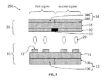
- FIG. 1 illustrates a schematic cross-section view of a liquid crystal display panel consistent with disclosed embodiments.
- FIG. 2 illustrates a schematic view of the polarization directions of different regions of the polarization layers in the liquid crystal display panel shown in FIG. 1 ;
- FIG. 3 illustrates a flowchart of an exemplary method for fabricating a regionalized polarization layer of liquid crystal display panel consistent with disclosed embodiments
- FIG. 4 illustrates a processing diagram of the irradiation process for fabricating a regionalized polarization layer consistent with disclosed embodiments
- FIG. 5 illustrates a schematic cross-section view of the structure of a display panel consistent with disclosed embodiments.
- FIG. 6 illustrates a schematic view of the polarization directions of different regions of the polarization layers in the display panel shown in FIG. 5 .
- FIG. 1 shows a schematic structure view of a liquid crystal display panel consistent with one embodiment of the present disclosure.
- the liquid crystal display panel 100 includes a thin-film transistor (TFT) substrate 10 , a color film substrate 30 arranged corresponding to the TFT substrate, and a liquid crystal layer 20 located between the TFT substrate 10 and the color film substrate 30 .
- TFT thin-film transistor
- Other components may also be included.
- the structure and the type of the liquid crystal display panel 100 are not limited to any specific type.
- the liquid crystal display panel 100 may be a Fringe Field Switching (FFS) type, an In-Plane Switching (IPS) type, or any other type.
- the liquid crystal display panel 100 is an FFS type liquid crystal display panel.
- the pixel structure of the liquid crystal display panel 100 is also not limited to any specific type and it can be single domain, double domain, or pseudo-double domain. In one embodiment, the pixel structure of the liquid crystal display panel 100 is a single domain type.
- the TFT array substrate 10 may include a first substrate 11 , a number of electrodes 12 , and a first polarization layer 13 .
- the electrodes 12 are arranged in parallel and spaced on the surface of the first substrate 11 close to the liquid crystal layer 20 .
- the electrodes 12 include a number of pixel electrodes and a number of common electrodes.
- the plurality of electrodes 12 are arranged in parallel with each other and extend along a direction D 5 (not shown).
- the first polarization layer 13 is arranged on the far-side surface of the first substrate 11 away from the liquid crystal layer 20 .
- the liquid crystal layer 20 is arranged between the TFT array substrate 10 and the color film substrate 30 .
- the liquid crystal layer 20 may be made of any appropriate liquid crystal material with a positive or a negative dielectric anisotropy.
- the liquid crystal molecules in the liquid crystal layer 20 are initially aligned along a direction D 1 (not shown). That is, the initial alignment direction of the liquid crystal molecules in the liquid crystal layer 20 extends along the direction D 1 .
- the liquid crystal molecules in the liquid crystal layer 20 have a positive dielectric anisotropy.
- the initial alignment direction D 1 of the positive liquid crystals has a first angle with respect to the extending direction D 5 of the electrodes 12 and the first angle is greater than 0 degree but less than or equal to 15 degrees.
- the color film substrate 30 includes a second substrate 31 , a number of color barriers 32 , a black matrix 33 , and a second polarization layer 34 .
- the plurality of color barriers 32 are arranged on the surface of the second substrate 31 close to the liquid crystal layer 20 .
- the second polarization layer 34 is arranged on the far-side surface of the second substrate 31 away from the liquid crystal layer 20 .
- the black matrix 33 is arranged in between multiple color barriers 32 .
- FIG. 2 shows a schematic view of the polarization directions of the polarization layers in the display panel shown in FIG. 1 .
- each of the first polarization layer 13 and the second polarization layer 34 may be a regionalized polarizer.
- the regionalized polarizer has at least one region having a polarization direction different from the polarization direction of other regions of the regionalized polarizer.
- At least one first region and at least one second region are defined in each of the first polarization layer 13 and the second polarization layer 34 .
- Each first region and each second region may individually correspond to one pixel or one subpixel.
- the first polarization layer 13 and the second polarization layer 34 have a first polarization region 132 and a second polarization region 342 , respectively.
- the first polarization layer 13 and the second polarization layer 34 have a third polarization region 134 and a fourth polarization region 344 , respectively.
- the polarization direction of the first polarization region 132 is different from the polarization direction of the second polarization region 342 ; while the polarization direction of the third polarization region 134 is different from the polarization direction of the fourth polarization region 344 .
- the absorption axis of the first polarization region 132 extends along the direction D 1 . That is, the absorption axis of the first polarization region 132 coincides with the initial alignment direction D 1 of the liquid crystal molecules.
- the absorption axis of the second polarization region 342 extends along a direction D 2 .
- the direction D 1 and the direction D 2 are perpendicular to each other.
- the absorption axis of the third polarization region 134 extends along a direction D 3 .
- the direction D 3 forms a second angle and a third angle with the direction D 1 and the direction D 5 , respectively.
- the second angle and the third angle are both greater than 0 degree and less than 90 degrees.
- the absorption axis of the fourth polarization region 344 extends along a direction D 4 .
- the direction D 3 and the direction D 4 are perpendicular to each other.
- the response speed and the driving voltage applied on a liquid crystal display device may satisfy the following relationship:
- ⁇ ON ⁇ 1 ⁇ d 2 ⁇ 0 ⁇ ⁇ ⁇ ⁇ ⁇ ⁇ ( V 2 - V TH 2 ) ( 1 )
- ⁇ OFF ⁇ 1 ⁇ d 2 ⁇ 2 ⁇ K ( 2 )
- ⁇ ON is the rise time, usually referring to the time during which the brightness of the liquid crystal display device increases from 10% (dark mode) of the maximum brightness to 90% (bright mode) of the maximum brightness
- ⁇ OFF is the fall time, usually referring to the time during which the brightness of the liquid crystal display device changes from the bright mode to the dark mode
- V is the driving voltage of the liquid crystal display device
- ⁇ 1 is the rotation viscosity coefficient of the liquid crystal
- ⁇ 0 is vacuum dielectric constant
- ⁇ ⁇ is the dielectric anisotropy constant
- V TH is the threshold voltage
- K is the effective elastic constant
- d is the thickness of the liquid crystal layer in the liquid crystal display device.
- the rise time of the liquid crystal display device decreases as the driving voltage increases.
- the fall time does not depend on the driving voltage.
- the response time of a liquid crystal display device is the sum of the rise time and the fall time and, therefore, a relatively effective method to decrease the response time is to decrease the rise time by increasing the driving voltage.
- the alignment direction of the liquid crystal molecules coincides with at least one of the absorption axes of two polarization layers, thus the initial state of the liquid crystal display device is set to the dark mode.
- the driving voltage to switch the device from the dark mode to the bright mode is limited within a relatively narrow voltage range. Therefore, the method to reduce the rise time by increasing the driving voltage is technically difficult.
- the third angle formed by the direction D 3 and the direction D 5 is further set to be greater than the first angle. Because the direction D 3 of the absorption axis of the third polarization region 134 of the first polarization layer 13 is different from the initial alignment direction D 1 of the liquid crystal molecules, and the third angle formed by the direction D 3 of the absorption axis of the third polarization region 134 and the extending direction D 5 of the electrodes 12 is greater than the first angle formed by the initial alignment direction D 1 of the liquid crystal molecules and the extending direction D 5 of the electrodes 12 , the initial state of the entire second region is not set to the dark mode.
- a preset voltage V 0 is required to be applied on the electrodes 12 in the entire second region in order to drive the second region into the dark mode. Further, in addition to the preset voltage V 0 , an extra driving voltage V may be applied on the electrodes 12 to drive the second region into the bright mode. That is, the driving voltage of the second region is V 0 +V. Therefore, the second region of the liquid crystal display panel 100 has a relatively large driving voltage, thus the rise time may be reduced, leading to an improved response speed.
- the initial state of the first region is the dark mode and no additional preset voltage V 0 is required. That is, the driving voltage of the first region is V. Therefore, the rise time and the response speed remain unchanged.
- the direction of the absorption axis of the first polarization region 132 may be set to have a preset angle with respect to the initial alignment direction D 1 of the liquid crystal molecules so that the initial state of the first region is not the dark mode. Further, by applying a preset voltage V 0 ′ on the electrodes 12 , the response speed of the first region may be improved.
- a liquid crystal display panel may be the same as the display panel described above, except that the absorption axis of the first polarization layer in the first region extends along a different direction from the initial polarization direction of the liquid crystal molecules in the liquid crystal layer of the display panel.
- the initial polarization direction of the liquid crystal molecules is along a first direction; while the absorption axis of the first polarization layer in the first region extends along a second direction.
- a first angle formed by the first direction and the second direction is greater than 0 degree but smaller than 90 degrees.
- the absorption axis of the second polarization layer in the first region is perpendicular to the absorption axis of the first polarization layer in the first region.
- the absorption axis of the first polarization layer extends along a third direction.
- the angle formed by the third direction and the second direction is defined as a second angle and it is greater than 0 degree but less than 90 degrees.
- the absorption axis of the second polarization layer is perpendicular to the absorption axis of the first polarization layer.
- a preset voltage is required for both the first region and the second region in order to drive them into the dark mode. Further, in addition to the preset voltage, an extra driving voltage may be applied to drive either one of the first region and the second region into the bright mode. Therefore, both the first region and the second region of the liquid crystal display panel have a relatively large driving voltage, thus the rise time may be reduced, leading to an improved response speed for both regions.
- the regionalized polarizers may include a base material and a polarizing material.
- the polarizing material may be doped into the base material.
- the base material may be one or more of cellulose triacetate, polyimide, polyamide acid, etc.
- the base material may have excellent photo-alignment properties. Under irradiation of polarized ultraviolet light, the base material may take a certain direction, correspondingly, the direction of the polarizing material also changes, and a certain alignment direction is then achieved.
- the polarizing material may include a dichroic organic dye with a dichroic ratio greater of equal to 7.
- the dichroic organic dye may be one or more of azo dye, anthraquinone dye, biphenyl dye, triphenyl dioxazine dye and derivatives, single-methine dye, multi-methine dye, poly ring dye, etc.
- the dichroic organic dye can be aligned under irradiation of polarized ultraviolet light.
- these dichroic organic dyes because of the dichroic property of these dichroic organic dyes, only light with a certain polarization direction is transmitted under the irradiation of natural light, while the light with the other polarization direction is blocked; therefore, these dichroic organic dyes may function as polarizer.
- azo dichroic organic dye may be:
- the difference in the polarization directions of different regions of a polarizer may be defined more accurately. Therefore, the accuracy of the regionalized polarizer is improved and the stability of the polarizer is also improved. The reason for this improvement might be that, by introducing the electron donating/attracting groups, the dichroic properties of the material are improved.
- the polarizing material may further include materials with a structure of benzidine, diphenyl urea, stilbene, two naphthylamine, J-acid, or anthraquinone.
- FIG. 3 illustrates a flowchart of an exemplary method for fabricating a regionalized polarization layer in the liquid crystal display panel consistent with disclosed embodiments.
- the regionalized polarization layer may be formed by the following fabrication procedures:
- Step S 1 providing a substrate.
- the substrate may be made of any appropriate material, such as quartz, glass, or resin.
- Step S 2 coating a mixture of the base material and the polarizing material or its precursor material onto the surface of the substrate.
- the mixture may be coated by a spin-coating method.
- a mixture of polyimide and azo dye is coated on the substrate.
- Step S 3 prebaking the polarization layer to form a first preform.
- the prebaking temperature may be in a range of 90° C. ⁇ 130° C. and the prebaking time may be in a range of 60 s ⁇ 120 s. In one embodiment, the prebaking temperature is about 130° C., while the prebaking time is about 120 s.
- Step S 4 Defining at least two regions on the first preform and irradiating the defined different regions using polarized ultraviolet light with different polarization directions to form a second preform;
- Irradiating the first preform with polarized ultraviolet light may let the polarizing material and/or the base material aligned along certain direction.
- the energy of the polarized ultraviolet light may be in a range of 300 mJ ⁇ 1000 mJ. In one embodiment, the energy of the polarized ultraviolet light is selected to be in a range of 500 mJ ⁇ 800 mJ. Using this irradiation energy, the photo-alignment properties of polyimide films may be desired. Thus, the irradiation energy helps the alignment of the azo dye, and desired polarization performance may be achieved.
- FIG. 4 shows a schematic diagram of the irradiating process for fabricating a regionalized polarization layer consistent with disclosed embodiments.
- the first preform may have a region A and a region B, and may be placed under a polarized ultraviolet light source.
- a mask plate for the irradiating process may be placed between the polarized ultraviolet light source and the first preform.
- the polarized ultraviolet light source and the mask plate are provided.
- the polarized ultraviolet light source can generate ultraviolet light polarized along the first polarization direction.
- the mask plate has at least one transparent area and one light-shielding area.
- region B of the first preform is shielded by the shielding area of the mask plate while region A of the first preform is exposed through the transparent area of the mask plate.
- the polarized ultraviolet light source is used to irradiate the exposed region A so that region A of the first preform is aligned.
- the first preform is then rotated by a certain angle so that the desired second polarization direction of the regionalized polarization layer to be formed now coincides with the polarization direction of the ultraviolet light.
- the shielding area of the mask plate is changed to cover region A of the first preform while the transparent area of the mask plate is used to expose region B of the first preform.
- the polarized ultraviolet light source is used to irradiate the exposed region B so that region B of the first preform is aligned along the second polarization direction.
- the irradiating process further includes Step S 5 : curing baking the second preform to form the regionalized polarization layer.
- the curing baking temperature may be in a range of 210° C. ⁇ 230° C. and the curing baking time may be in a range of 20 min ⁇ 50 min. In one embodiment, the curing baking temperature is about 230° C., while the curing baking time is about 30 min.
- liquid crystal display panels using regionalized polarization layers of the present disclosure may also realize 3D display functions.
- the present disclosure further provides a display device containing the liquid crystal display panel 100 described above.
- FIG. 5 shows a schematic cross-section view of the structure of a display panel consistent with another embodiment of the present disclosure.
- FIG. 6 shows a schematic view of the polarization directions of different regions of the polarization layers in the display panel shown in FIG. 5 .
- the liquid crystal display panel 200 in the present embodiment is substantially the same as the display panel 100 shown in FIG. 1 and FIG. 2 , except that the liquid crystal molecules in the liquid crystal layer 20 of the display panel 200 have a negative dielectric anisotropy, and the polarization directions of the first polarization layer 13 and the second polarization layer 34 in the first region and the second region are different.
- a first angle formed by an initial alignment direction D 1 of the negative liquid crystals and an extending direction D 5 of electrodes 12 is greater than 75 degrees but less than or equal to 90 degrees.
- the absorption axis of a first polarization region 136 coincides with the initial alignment direction D 1 of the liquid crystal molecules.
- the absorption axis of a second polarization region 346 extends along a direction D 2 .
- the direction D 1 and the direction D 2 are perpendicular to each other.
- the absorption axis of a third polarization region 138 extends along a direction D 3 .
- the direction D 3 forms a second angle and a third angle with the direction D 1 and the direction D 5 , respectively.
- the second angle and the third angle are both greater than 0 degree and less than 90 degrees.
- the absorption axis of a fourth polarization region 348 extends along a direction D 4 .
- the direction D 3 and the direction D 4 are perpendicular to each other.
- the third angle formed by the direction D 3 and the direction D 5 is smaller than the first angle formed by the initial alignment direction D 1 of the liquid crystal molecules and the extending direction D 5 of electrodes 12 .
- the initial state of the entire second region is not set to the dark mode. Therefore, a preset voltage V 0 is required to be applied on the electrodes 12 in the entire second region in order to drive the second region into the dark mode.
- an extra driving voltage V may be applied on the electrodes 12 to drive the second region into the bright mode. That is, the driving voltage of the second region is V 0 +V. Therefore, the second region of the liquid crystal display panel 200 has a relatively large driving voltage, thus the rise time may be reduced, leading to an improved response speed.
- the initial state of the first region is the dark mode and no additional preset voltage V 0 is required. That is, the driving voltage of the first region is V. Therefore, the rise time and the response speed remain unchanged.
- the disclosed liquid crystal display panel and the liquid crystal display device of the present disclosure may have the following advantages: first, by increasing the driving voltage of the second region, the response speed of the second region is improved; second, driving voltage in only part of the region, instead of the entire region, of the liquid crystal display panel and the liquid crystal display device is increased, thus the energy consumption remains low; and, finally, because of the use of the regionalized polarization layers, the liquid crystal display panel and the liquid crystal display device may also have 3D display functions.
- the initial state of the second polarization region is not in a dark mode.
- a preset voltage V 0 applied on the electrode of the entire second polarization region is required to achieve a dark mode.
- a driving voltage V is required to achieve a bright mode in the second region. Therefore, the response speed of the second region is improved.
- the liquid crystal display panel and the liquid crystal display device of the present disclosure may also have 3D display functions.
Landscapes
- Physics & Mathematics (AREA)
- Nonlinear Science (AREA)
- Mathematical Physics (AREA)
- Chemical & Material Sciences (AREA)
- Crystallography & Structural Chemistry (AREA)
- General Physics & Mathematics (AREA)
- Optics & Photonics (AREA)
- Geometry (AREA)
- Spectroscopy & Molecular Physics (AREA)
- Liquid Crystal (AREA)
- Engineering & Computer Science (AREA)
- Microelectronics & Electronic Packaging (AREA)
Abstract
Description

Claims (19)
Applications Claiming Priority (3)
| Application Number | Priority Date | Filing Date | Title |
|---|---|---|---|
| CN2015-10076358.7 | 2015-02-13 | ||
| CN201510076358 | 2015-02-13 | ||
| CN201510076358.7A CN104635373B (en) | 2015-02-13 | 2015-02-13 | Liquid crystal display panel and liquid crystal display device |
Publications (2)
| Publication Number | Publication Date |
|---|---|
| US20160238891A1 US20160238891A1 (en) | 2016-08-18 |
| US9804439B2 true US9804439B2 (en) | 2017-10-31 |
Family
ID=53214299
Family Applications (1)
| Application Number | Title | Priority Date | Filing Date |
|---|---|---|---|
| US15/044,205 Expired - Fee Related US9804439B2 (en) | 2015-02-13 | 2016-02-16 | Display panel and a display device |
Country Status (2)
| Country | Link |
|---|---|
| US (1) | US9804439B2 (en) |
| CN (1) | CN104635373B (en) |
Cited By (1)
| Publication number | Priority date | Publication date | Assignee | Title |
|---|---|---|---|---|
| US20230176405A1 (en) * | 2021-12-02 | 2023-06-08 | Coretronic Corporation | Display apparatus and method of driving the same |
Families Citing this family (1)
| Publication number | Priority date | Publication date | Assignee | Title |
|---|---|---|---|---|
| CN108628033A (en) * | 2018-05-10 | 2018-10-09 | 京东方科技集团股份有限公司 | Curved display panel and curved display device |
Citations (12)
| Publication number | Priority date | Publication date | Assignee | Title |
|---|---|---|---|---|
| EP0525478A2 (en) | 1991-07-26 | 1993-02-03 | F. Hoffmann-La Roche Ag | Liquid crystal display cell |
| CN1716055A (en) | 2004-06-30 | 2006-01-04 | Lg.菲利浦Lcd株式会社 | Liquid crystal display device and method for fabricating the same |
| US20060139574A1 (en) * | 2004-12-29 | 2006-06-29 | Ralli Philip J | Projection system including intrinsic polarizer |
| US20080170183A1 (en) * | 2007-01-16 | 2008-07-17 | Seiko Epson Corporation | Electrooptic device, electronic apparatus, and driving method for the electrooptic device |
| CN101726925A (en) | 2008-11-03 | 2010-06-09 | 上海天马微电子有限公司 | Method for improving response speed of liquid crystal display device and liquid crystal display device |
| US20100208176A1 (en) * | 2009-02-17 | 2010-08-19 | Chi Mei Optoelectronics Corporation | Wide Viewing Angle Transflective Liquid Crystal Displays |
| US20110141127A1 (en) * | 2009-12-15 | 2011-06-16 | Wistron Corporation | Data producing method and electronic device thereof |
| US20110242468A1 (en) * | 2010-04-02 | 2011-10-06 | Samsung Electronics Co., Ltd. | Pixel electrode panel, a liquid crystal display panel assembly and methods for manufacturing the same |
| US20130120676A1 (en) * | 2010-06-18 | 2013-05-16 | Fujifilm Corporation | Stereo image print and method of producing the same |
| US20140118665A1 (en) * | 2012-10-31 | 2014-05-01 | Japan Display Inc. | Liquid crystal display device |
| CN104122703A (en) | 2013-09-30 | 2014-10-29 | 深超光电(深圳)有限公司 | Liquid crystal display device, manufacturing method thereof and electronic device |
| CN104220965A (en) | 2012-01-26 | 2014-12-17 | 柯尼卡美能达株式会社 | Touch-panel-equipped liquid crystal display device |
-
2015
- 2015-02-13 CN CN201510076358.7A patent/CN104635373B/en not_active Expired - Fee Related
-
2016
- 2016-02-16 US US15/044,205 patent/US9804439B2/en not_active Expired - Fee Related
Patent Citations (12)
| Publication number | Priority date | Publication date | Assignee | Title |
|---|---|---|---|---|
| EP0525478A2 (en) | 1991-07-26 | 1993-02-03 | F. Hoffmann-La Roche Ag | Liquid crystal display cell |
| CN1716055A (en) | 2004-06-30 | 2006-01-04 | Lg.菲利浦Lcd株式会社 | Liquid crystal display device and method for fabricating the same |
| US20060139574A1 (en) * | 2004-12-29 | 2006-06-29 | Ralli Philip J | Projection system including intrinsic polarizer |
| US20080170183A1 (en) * | 2007-01-16 | 2008-07-17 | Seiko Epson Corporation | Electrooptic device, electronic apparatus, and driving method for the electrooptic device |
| CN101726925A (en) | 2008-11-03 | 2010-06-09 | 上海天马微电子有限公司 | Method for improving response speed of liquid crystal display device and liquid crystal display device |
| US20100208176A1 (en) * | 2009-02-17 | 2010-08-19 | Chi Mei Optoelectronics Corporation | Wide Viewing Angle Transflective Liquid Crystal Displays |
| US20110141127A1 (en) * | 2009-12-15 | 2011-06-16 | Wistron Corporation | Data producing method and electronic device thereof |
| US20110242468A1 (en) * | 2010-04-02 | 2011-10-06 | Samsung Electronics Co., Ltd. | Pixel electrode panel, a liquid crystal display panel assembly and methods for manufacturing the same |
| US20130120676A1 (en) * | 2010-06-18 | 2013-05-16 | Fujifilm Corporation | Stereo image print and method of producing the same |
| CN104220965A (en) | 2012-01-26 | 2014-12-17 | 柯尼卡美能达株式会社 | Touch-panel-equipped liquid crystal display device |
| US20140118665A1 (en) * | 2012-10-31 | 2014-05-01 | Japan Display Inc. | Liquid crystal display device |
| CN104122703A (en) | 2013-09-30 | 2014-10-29 | 深超光电(深圳)有限公司 | Liquid crystal display device, manufacturing method thereof and electronic device |
Cited By (2)
| Publication number | Priority date | Publication date | Assignee | Title |
|---|---|---|---|---|
| US20230176405A1 (en) * | 2021-12-02 | 2023-06-08 | Coretronic Corporation | Display apparatus and method of driving the same |
| US11841565B2 (en) * | 2021-12-02 | 2023-12-12 | Coretronic Corporation | Display apparatus having adjustable viewing angle range and method of driving the same |
Also Published As
| Publication number | Publication date |
|---|---|
| CN104635373B (en) | 2018-03-16 |
| CN104635373A (en) | 2015-05-20 |
| US20160238891A1 (en) | 2016-08-18 |
Similar Documents
| Publication | Publication Date | Title |
|---|---|---|
| JP6317582B2 (en) | Liquid crystal display and manufacturing method thereof | |
| US9140936B2 (en) | Blue phase liquid crystal panel and display device | |
| ITUD980090A1 (en) | METHOD OF PRODUCING TWO DOMAINS INSIDE A LAYER OF LIQUID CRYSTAL, A DISPLAY DEVICE A | |
| CN104160326B (en) | Liquid crystal indicator | |
| US10649266B2 (en) | Liquid crystal display and display device | |
| US9261740B2 (en) | Liquid crystal panel | |
| US10114249B2 (en) | Liquid crystal display panel and fabrication method thereof | |
| US20160238897A1 (en) | Display panel and a display device | |
| US10133115B2 (en) | Color filter and manufacturing method thereof, liquid crystal display panel | |
| US20160266438A1 (en) | Transflective liquid crystal display device | |
| WO2017063231A1 (en) | Liquid crystal display panel | |
| US20130329151A1 (en) | Liquid crystal panel, manufacturing process and display device thereof | |
| US10203556B2 (en) | Display substrate having pre-tilt angle for liquid crystal molecules | |
| US9804439B2 (en) | Display panel and a display device | |
| KR20130101326A (en) | Liquid crystal display and manufacturing method thereof | |
| US9581869B2 (en) | In-plane switching mode liquid crystal display device and fabrication method thereof | |
| CN109188784B (en) | Display substrate, manufacturing method thereof and display device | |
| US9588393B2 (en) | Liquid crystal panel and method of manufacturing the same, display device | |
| US10459297B2 (en) | Liquid crystal display device including liquid crystal capsule and method of fabricating the same | |
| US20150077683A1 (en) | Liquid crystal display panel and display apparatus using the same | |
| KR102242168B1 (en) | Curved liquid crystal display panel, curved liquid crystal display device including the same and manufacturing of the same | |
| US9235088B1 (en) | Liquid crystal display panel and fabrication method for the same | |
| US20210364851A1 (en) | Curved display device | |
| JP2023089664A (en) | liquid crystal display | |
| US9487699B2 (en) | Liquid crystal display panel and liquid crystal display apparatus having the same |
Legal Events
| Date | Code | Title | Description |
|---|---|---|---|
| AS | Assignment |
Owner name: SHANGHAI TIANMA MICRO-ELECTRONICS CO., LTD, CHINA Free format text: ASSIGNMENT OF ASSIGNORS INTEREST;ASSIGNORS:CAO, ZHAOKENG;HUANG, ZHONGSHOU;ZHANG, LONG;REEL/FRAME:037739/0251 Effective date: 20160213 Owner name: TIANMA MICRO-ELECTRONICS CO., LTD., CHINA Free format text: ASSIGNMENT OF ASSIGNORS INTEREST;ASSIGNORS:CAO, ZHAOKENG;HUANG, ZHONGSHOU;ZHANG, LONG;REEL/FRAME:037739/0251 Effective date: 20160213 |
|
| STCF | Information on status: patent grant |
Free format text: PATENTED CASE |
|
| MAFP | Maintenance fee payment |
Free format text: PAYMENT OF MAINTENANCE FEE, 4TH YEAR, LARGE ENTITY (ORIGINAL EVENT CODE: M1551); ENTITY STATUS OF PATENT OWNER: LARGE ENTITY Year of fee payment: 4 |
|
| FEPP | Fee payment procedure |
Free format text: MAINTENANCE FEE REMINDER MAILED (ORIGINAL EVENT CODE: REM.); ENTITY STATUS OF PATENT OWNER: LARGE ENTITY |
|
| LAPS | Lapse for failure to pay maintenance fees |
Free format text: PATENT EXPIRED FOR FAILURE TO PAY MAINTENANCE FEES (ORIGINAL EVENT CODE: EXP.); ENTITY STATUS OF PATENT OWNER: LARGE ENTITY |
|
| STCH | Information on status: patent discontinuation |
Free format text: PATENT EXPIRED DUE TO NONPAYMENT OF MAINTENANCE FEES UNDER 37 CFR 1.362 |
|
| FP | Lapsed due to failure to pay maintenance fee |
Effective date: 20251031 |