US9800348B2 - Chromatic dispersion estimation for digital coherent optical receivers - Google Patents
Chromatic dispersion estimation for digital coherent optical receivers Download PDFInfo
- Publication number
- US9800348B2 US9800348B2 US14/546,976 US201414546976A US9800348B2 US 9800348 B2 US9800348 B2 US 9800348B2 US 201414546976 A US201414546976 A US 201414546976A US 9800348 B2 US9800348 B2 US 9800348B2
- Authority
- US
- United States
- Prior art keywords
- signal
- component
- costs
- digital
- optical
- Prior art date
- Legal status (The legal status is an assumption and is not a legal conclusion. Google has not performed a legal analysis and makes no representation as to the accuracy of the status listed.)
- Active, expires
Links
- 230000003287 optical effect Effects 0.000 title claims abstract description 129
- 239000006185 dispersion Substances 0.000 title claims abstract description 16
- 230000001427 coherent effect Effects 0.000 title claims description 25
- 238000000034 method Methods 0.000 claims description 78
- 230000010287 polarization Effects 0.000 claims description 31
- 230000005540 biological transmission Effects 0.000 claims description 16
- 230000000694 effects Effects 0.000 claims description 15
- 230000010363 phase shift Effects 0.000 claims description 4
- 238000009825 accumulation Methods 0.000 claims 3
- 230000035508 accumulation Effects 0.000 claims 3
- 238000012545 processing Methods 0.000 abstract description 50
- 230000006870 function Effects 0.000 description 39
- 230000006735 deficit Effects 0.000 description 20
- 238000004891 communication Methods 0.000 description 15
- 238000010586 diagram Methods 0.000 description 10
- 230000007246 mechanism Effects 0.000 description 8
- 230000015654 memory Effects 0.000 description 8
- 238000013461 design Methods 0.000 description 7
- 239000000835 fiber Substances 0.000 description 7
- 230000004044 response Effects 0.000 description 7
- 238000012937 correction Methods 0.000 description 5
- 239000013307 optical fiber Substances 0.000 description 5
- 230000000644 propagated effect Effects 0.000 description 5
- 238000003860 storage Methods 0.000 description 5
- 238000004590 computer program Methods 0.000 description 4
- 238000005516 engineering process Methods 0.000 description 4
- 230000008569 process Effects 0.000 description 3
- 238000011084 recovery Methods 0.000 description 3
- 238000007476 Maximum Likelihood Methods 0.000 description 2
- 238000013459 approach Methods 0.000 description 2
- 230000008859 change Effects 0.000 description 2
- 230000001419 dependent effect Effects 0.000 description 2
- 238000001514 detection method Methods 0.000 description 2
- 238000001914 filtration Methods 0.000 description 2
- 230000007774 longterm Effects 0.000 description 2
- 238000005259 measurement Methods 0.000 description 2
- 239000000203 mixture Substances 0.000 description 2
- 230000002441 reversible effect Effects 0.000 description 2
- 230000011664 signaling Effects 0.000 description 2
- 238000009987 spinning Methods 0.000 description 2
- 238000010408 sweeping Methods 0.000 description 2
- 238000012546 transfer Methods 0.000 description 2
- 238000011144 upstream manufacturing Methods 0.000 description 2
- 230000003044 adaptive effect Effects 0.000 description 1
- 230000004075 alteration Effects 0.000 description 1
- 238000004458 analytical method Methods 0.000 description 1
- 230000001934 delay Effects 0.000 description 1
- 238000011161 development Methods 0.000 description 1
- 230000009977 dual effect Effects 0.000 description 1
- 238000004870 electrical engineering Methods 0.000 description 1
- 230000009021 linear effect Effects 0.000 description 1
- 238000004519 manufacturing process Methods 0.000 description 1
- 238000012986 modification Methods 0.000 description 1
- 230000004048 modification Effects 0.000 description 1
- 238000012544 monitoring process Methods 0.000 description 1
- 230000009022 nonlinear effect Effects 0.000 description 1
- 238000011160 research Methods 0.000 description 1
- 239000004065 semiconductor Substances 0.000 description 1
- 230000003595 spectral effect Effects 0.000 description 1
- 238000001228 spectrum Methods 0.000 description 1
- 230000002269 spontaneous effect Effects 0.000 description 1
- 230000007480 spreading Effects 0.000 description 1
- 238000003892 spreading Methods 0.000 description 1
- 230000003068 static effect Effects 0.000 description 1
- 238000006467 substitution reaction Methods 0.000 description 1
- 230000001131 transforming effect Effects 0.000 description 1
Images


Classifications
-
- H—ELECTRICITY
- H04—ELECTRIC COMMUNICATION TECHNIQUE
- H04B—TRANSMISSION
- H04B10/00—Transmission systems employing electromagnetic waves other than radio-waves, e.g. infrared, visible or ultraviolet light, or employing corpuscular radiation, e.g. quantum communication
- H04B10/60—Receivers
- H04B10/61—Coherent receivers
- H04B10/616—Details of the electronic signal processing in coherent optical receivers
- H04B10/6161—Compensation of chromatic dispersion
-
- H—ELECTRICITY
- H04—ELECTRIC COMMUNICATION TECHNIQUE
- H04B—TRANSMISSION
- H04B10/00—Transmission systems employing electromagnetic waves other than radio-waves, e.g. infrared, visible or ultraviolet light, or employing corpuscular radiation, e.g. quantum communication
- H04B10/60—Receivers
- H04B10/61—Coherent receivers
- H04B10/613—Coherent receivers including phase diversity, e.g., having in-phase and quadrature branches, as in QPSK coherent receivers
-
- H—ELECTRICITY
- H04—ELECTRIC COMMUNICATION TECHNIQUE
- H04B—TRANSMISSION
- H04B10/00—Transmission systems employing electromagnetic waves other than radio-waves, e.g. infrared, visible or ultraviolet light, or employing corpuscular radiation, e.g. quantum communication
- H04B10/60—Receivers
- H04B10/61—Coherent receivers
- H04B10/614—Coherent receivers comprising one or more polarization beam splitters, e.g. polarization multiplexed [PolMux] X-PSK coherent receivers, polarization diversity heterodyne coherent receivers
Definitions
- An optical communication system may comprise an optical transmitter, a channel (e.g., optical fibers), and an optical receiver.
- the optical transmitter may encode data onto an optical signal
- the channel may carry the optical signal from the transmitter to the receiver
- the receiver may recover the data from the received optical signal.
- One type of optical communication system may be a long-haul optical communication system, in which data may be carried through optical transmission links and/or optical fibers that span long distances.
- Long-haul optical communication systems may increase data rates by employing coherent optical transmissions, in which data may be modulated onto amplitudes, phases, and/or polarization components of an optical carrier signal.
- ISI inter-symbol interference
- CD chromatic dispersion
- PMD polarization mode dispersion
- phase noise non-linear effects
- CD may cause different spectral components (e.g., wavelengths) in a light signal to travel through an optical fiber at different speeds and arrive at a receiver at different time instants, and thus may broaden the light pulses that carry the data and lead to ISI.
- Some systems may compensate CD in a fiber by employing another fiber of opposite-sign dispersion, but may be at the expense of an increased non-linearity effect.
- ADCs analog-to-digital converters
- DACs digital-to-analog converters
- DSPs digital signal processors
- the disclosure includes an apparatus comprises a front end configured to receive an optical signal, and convert the optical signal into a plurality of digital signals, and a processing unit coupled to the front end and configured to determine a best-match CD estimate in the optical signal by optimizing a cost function based on signal peaks of the plurality of digital signals.
- the disclosure includes a method for estimating CD in an optical device coupled to an optical transmission link, the method comprising receiving an optical signal via the optical transmission link, converting the optical signal into a plurality of digital signals, and determining a best-match CD estimate associated with the optical signal by optimizing a cost function based on signal peaks of the plurality of digital signals.
- the disclosure includes a coherent optical receiver comprising a front end configured to receive an optical signal, and convert the optical signal into a plurality of digital electrical signals, one or more frequency domain equalizers (FDEQs) coupled to an output of the front end and configured to compensate CD in the optical signal, and a CD estimation (CDE) unit coupled to the FDEQs and configured to determine a best-match CD estimate associated with the optical signal by optimizing a cost function based on a summation of signal peaks, wherein the best-match CD estimate is used by the FDEQs to compensate the CD in the optical signal.
- FDEQs frequency domain equalizers
- CDE CD estimation
- FIG. 1 is a schematic diagram of an embodiment of an optical transportation link.
- FIG. 2 is a schematic diagram of an embodiment of a digital receiver processing module.
- FIG. 3 is a schematic diagram of another embodiment of a digital receiver processing module.
- FIG. 4 is a schematic diagram of an embodiment of another digital receiver processing module.
- FIG. 5 is a flowchart of an embodiment of a method for estimating CD.
- FIG. 6 is a flowchart of another embodiment of a method for estimating CD.
- FIG. 7 illustrates an embodiment of a table comparing DSP complexity for a clock-tone (CT)-energy-based CDE method, a peak-to-average power ratio (PAPR)-based CDE method, and a signal-peak-based CDE method.
- CT clock-tone
- PAPR peak-to-average power ratio
- FIG. 8 is a graph showing an embodiment of a CD cost function in the presence of CD and narrow band electrical filters.
- FIG. 9 is a graph showing an embodiment of a CD cost function in the presence of CD and wavelength selective switches (WSSs).
- FIG. 10 is a graph showing an embodiment of a CD cost function in the presence of CD and other channel impairments.
- FIG. 11 is a schematic diagram of an embodiment of a transceiver unit.
- FDEQs may be widely employed for CD compensation in digital coherent optical receivers due to the low computational complexity for compensating CD with large dispersions and in long fiber distances.
- CD may be quasi-static for a given optical channel (e.g., a transmission link with fixed fiber type and fiber length) and may affect the phase of a signal in the frequency domain, where the phase may vary according to the amount of CD in the optical channel.
- a receiver may configure the FDEQs to match the inverse function of the CD effect or the CD impulse response, for example, by adjusting FDEQ tap coefficients.
- the receiver may not have prior knowledge of the amount of CD effect.
- the receiver may estimate the amount of CD in the optical channel during an initial acquisition stage, for example, based on a received optical signal propagated through the optical channel. After estimating the CD in the received optical signal, the receiver may configure the FDEQs according to the CD estimate such that the FDEQs may substantially compensate the CD in subsequent received signals.
- the disclosed CDE may employ a best search approach by sweeping a range of FDEQs configured to compensate a range of CD candidates in a received optical signal and computing a signal-peak-based cost function to determine an optimum CD candidate that substantially matches the CD effect in the received optical signal.
- the FDEQ may be configured to compensate one of the CD candidates
- the received optical signal may be filtered by the FDEQ
- a goodness measure or cost for the CD candidate may be computed by accumulating signal peaks of the filtered signal.
- one FDEQ may be applied to each polarization comprising an in-phase (I) component and a quadrature-phase (Q) component.
- the goodness measure or cost may be computed by accumulating the magnitude of the maximum signal peak of each component of each polarization.
- the signal-peak-based cost function may operate based on the CD signal spreading effect. For example, when a signal is distorted by CD, the signal may spread, but the signal energy may remain the same, and thus the signal peaks may increase. As such, a CD-compensated signal may comprise smaller signal peaks. Thus, an optimum CDE may be determined by selecting a CD candidate that produces a minimum cost. Since the signal-peak-based CD cost function may not comprise complex operations, such as multiplications and/or divisions, the disclosed CDE mechanisms may be efficient for hardware and/or software implementations.
- the disclosed embodiments may be suitable for any optical transceivers, signaling schemes, modulation schemes, detection and/or equalization schemes, and/or multiplexing structures.
- the signaling schemes may include raised-cosine (RC), root-raised-cosine (RRC), non-return-to-zero (NRZ), and/or return-to-zero with 67 percent duty cycle (RZ67);
- the modulation schemes may include binary phase shift keying (BPSK), quadrature phase shift keying (QPSK), eight quadrature amplitude modulation (8-QAM), sixteen quadrature amplitude modulation (16-QAM), and/or higher order quadrature amplitude modulation;
- the detection and/or equalization schemes may include transmit pre-compensation, PMD compensation, and automatic spontaneous emission (ASE) noise compensation; and the multiplexing structures may include frequency-division multiplexing (FDM) and/or wavelength-division multiplexing (WDM).
- FDM frequency-division multiplexing
- the disclosed embodiments may provide robust CDEs in the presence of narrow band electrical filtering, networks with a large number of WSSs, a large local oscillator frequency offset (LOFO), a high parts-per-million (PPM) local oscillator (LO), high channel impairments, large ASE, etc.
- LOFO local oscillator frequency offset
- PPM parts-per-million
- FIG. 1 is a schematic diagram of an embodiment of an optical transportation link 100 .
- the optical transportation link 100 may comprise a transmitter 110 communicatively coupled to a coherent receiver 130 through an optical propagation channel 120 .
- the transmitter 110 may be located on a transmitting side of the link 100 and may be configured to send optical signals to the receiver 130 located on a receiving side of the optical link 100 via the channel 120 .
- the channel 120 may represent a transmission link in an optical communication network and may carry upstream and/or downstream transmission signals between a central office (CO) and a customer-premises equipment (CPE).
- CO central office
- CPE customer-premises equipment
- the transmitter 110 may reside at the CO and the receiver 130 may reside at the CPE for downstream transmission
- the transmitter 110 may reside at the CPE and the receiver 130 may reside at the CO.
- An optical transceiver at a CO and/or a CPE may comprise both the transmitter 110 and the receiver 130 in order to facilitate bi-directional data communications.
- the transmitter 110 may comprise electrical-to-optical (E/O) components (not shown), such as electrical drivers, E/O converters, and/or a laser.
- the E/O components may modulate electrical signals onto an optical carrier provided by the laser.
- the transmitter 110 may transmit an optical signal comprising two orthogonal linear-polarization components, an X-polarization component and a Y-polarization component.
- Each-polarization component may comprise two orthogonal phase components, an I component and a Q component, both comprising the same optical carrier frequency.
- the carrier frequency may be an optical wavelength supplied by the laser with phase noise.
- the channel 120 may comprise fiber 121 , optical filters 122 , optical amplifiers 123 , and/or other components.
- the optical channel 120 may comprise various types of channel impairments, for example, CD, non-linear phase noise, PMD, polarization dependent loss (PDL), polarization dependent gain, state-of-polarization (SOP) rotations, and optical white Gaussian noise.
- CD non-linear phase noise
- PMD polarization dependent loss
- PDL polarization dependent gain
- SOP state-of-polarization
- optical white Gaussian noise optical white Gaussian noise.
- the imperfections of components in the transmitter 110 and/or the receiver 120 and/or the mismatches between the transmitter 110 and the receiver 120 such as LOFO, LO inaccuracies, in-phase and quadrature-phase (IQ) imbalance, etc., may contribute to the noise received at the receiver 130 .
- LOFO LO inaccuracies
- IQ quadrature-phase
- the receiver 130 may comprise an integrated coherent receiver front end 131 , one or more ADCs 132 , and a DSP unit 133 .
- the receiver 130 may be configured to receive an optical signal transmitted by the transmitter 110 and propagated through the channel 120 .
- the integrated coherent receiver 131 may be configured to convert the received optical signal into one or more electrical signals.
- the integrated coherent receiver 131 may comprise a LO (not shown) and/or mixers (not shown).
- the LO which may have a frequency that closely matches the laser at the transmitter 110 , may mix with the propagated optical signal and split the propagated optical signal into four electrical signals (e.g., I and Q components for each X- and Y-polarization) with each split signal being a mixture of the transmitted signal.
- the ADCs 132 may be coupled to the integrated coherent receiver 131 and configured to convert the electrical signals into digital signals. It should be noted that the integrated coherent receiver front end 131 and the ADCs 132 may be referred to as the front end.
- the DSP unit 133 may be coupled to the ADCs 132 and may comprise one or more processors, which may include general processors, single-core processors, multi-core processors, application-specific integrated circuits (ASICs), and/or DSPs.
- the DSP unit 133 may be configured to process the digital signals to recover data transmitted by the transmitter 110 .
- the DSP unit 133 may compensate channel impairments caused by the channel 120 and/or hardware impairments caused by imperfections and/or mismatches in the hardware components between the transmitter 110 and the receiver 130 .
- the receiver 130 may employ a general processing unit instead of a DSP unit 133 , for example, when the general processing unit provides sufficient processing speed and meets the power consumption requirements of the receiver 130 .
- the general processing unit may comprise one or more general processors, single-core processors, multi-core processors, and/or ASICs.
- the optical transportation link 100 may be a long-haul transmission link.
- the DSP unit 133 may employ a multiple-input and multiple-output infinite impulse response (MIMO-IIR) adaptive equalizer with a large number of taps.
- MIMO-IIR multiple-input and multiple-output infinite impulse response
- Such an equalizer may be computationally complex and may be expensive to implement in hardware and/or software.
- One simpler approach may be to implement several different equalizers, each specifically designed to compensate a particular impairment based on the properties and/or the effect of the impairment.
- CD is a quasi-deterministic impairment (e.g., slow varying or about constant for a given transmission link) with long delays
- a static frequency domain zero-forcing equalizer or a mean-square error equalizer, such as an FDEQ may be suitable for compensating CD.
- the DSP unit 133 may employ other equalizers and/or circuits, for example, in the time domain, subsequent to the FDEQ to compensate other impairments, such as PMD, PDL, SOP, etc.
- FIG. 2 is a schematic diagram of an embodiment of a digital receiver processing module 200 , which may perform substantially similar functions as the DSP unit 133 .
- the digital receiver processing module 200 may be realized in hardware and/or implemented as DSP software components.
- the digital receiver processing module 200 may be configured to compensate impairments in an optical transportation link, such as link 100 .
- the digital receiver processing module 200 may comprise FDEQs 211 and 212 , a MIMO finite impulse response (FIR) unit 220 , a carrier phase recovery and correction unit 230 , and an forward error correction (FEC) unit 240 .
- FIR MIMO finite impulse response
- FEC forward error correction
- the FDEQs 211 and 212 may be configured as a match filter to reverse the impact of CD caused by an optical propagation channel, such as the channel 120 .
- the FDEQs 211 and 212 may perform CD compensation in the frequency domain.
- the FDEQs 211 and 212 may compensate CD in a received optical signal by multiplying the I and Q components of an X-polarization component and a Y-polarization component of the received optical signal with a frequency domain filter that is the inverse transfer function of a channel CD response, where the filter may be an all-pass filter with a parabolic phase that matches the amount of CD (e.g., in units of picoseconds per nanometer (ps/nm)) in the channel.
- CD compensation may be performed separately for each polarization.
- the FDEQ 211 may compensate CD in the X-polarization component by processing the corresponding I and Q components, denoted as X I and X Q , respectively
- the FDEQ 212 may compensate CD in the Y-polarization component by processing the corresponding I and Q components, denoted as Y I and Y Q , respectively.
- each FDEQ 211 and 212 may comprise a fast Fourier transform (FFT) unit that converts the I and Q components in the corresponding polarization into frequency domain signals prior to multiplying with the frequency domain filter and an inverse FFT (IFFT) unit that converts the filtered signals into the time domain.
- FFT fast Fourier transform
- IFFT inverse FFT
- the digital receiver processing module 200 may configure the filter by adjusting the filter tap coefficients according to the amount of CD.
- the MIMO FIR unit 220 may be coupled to the FDEQs 211 and 212 and may be configured to perform PMD and/or SOP equalization on the CD compensated X and Y-polarization signals, denoted as h(t) and v(t), respectively, each comprising a real component and an imaginary component.
- the carrier phase recovery and correction unit 230 may be coupled to the MIMO FIR unit 220 and configured to compensate laser line-width, low frequency laser phase noise, and/or low frequency fiber non-linearity phase noise.
- the FEC unit 240 may be coupled to the carrier phase recovery and correction unit 230 and configured to perform error correction according to predetermined error correcting codes.
- the frequency domain filters in the FDEQs 211 and 212 may be configured to match the amount of CD in the channel.
- the digital receiver processing module 200 may not have prior knowledge of the amount of CD effect.
- the digital receiver processing module 200 may estimate the CD effect in the presence of other impairments. The accuracies of the CD estimate may affect the performance of the digital receiver processing module 200 significantly since large CD error may not be removed by any other equalizers subsequent to the FDEQs 211 and 212 and may cause data decoding failure in the digital receiver processing module 200 .
- CDE methods may employ brute force or best-search mechanisms to blindly estimate CD from a received optical signal in the digital domain by sweeping over a range of CD candidate values, evaluating a cost function for each CD candidate value, and optimizing the cost function.
- the cost function may be based on CT energy as described in R. Soriano, et al., “Chromatic Dispersion Estimation in Digital Coherent Receivers,” Journal of Lightwave Technology, Vol. 29, No. 11, pp. 1627-1637, Jun. 1, 2011 and F. N. Hauske, et al., “Frequency Domain Chromatic Dispersion Estimation,” Optical Society of America, 2010which are incorporated by reference.
- the cost function may be based on PAPR as described in C. Xie, “Chromatic Dispersion Estimation for Single-Carrier Coherent Optical Communications,” Institute of Electrical and Electronics Engineers (IEEE) Photonic Technology Letters, Vol. 25, No. 10, May 15, 2013, which is incorporated by reference.
- the CT-energy-based cost function may evaluate the energy of a CT in a RC pulse-shaped signal spectrum at frequencies of about ⁇ 1 ⁇ 2 f B , where f B is the signal baud rate.
- the CT may comprise the highest amount of energy.
- LOFO e.g., shifts the CT frequency
- PMD e.g., at about 0.5 unit interval (UI) differential group delay (DGD)
- SOP rotations the CT-energy-based cost function may not provide an accurate CD estimate.
- the CT-energy-based or modified cost functions may be limited by electrical and/or optical bandwidth as the system data rate increases (e.g., with higher baud rates).
- the PAPR-based cost function may be less noise limiting, but may comprise high computational complexity.
- the PAPR-based cost function, J CD _ PAPR may be computed as shown below:
- J CD_PAPR max ⁇ ( ⁇ real ⁇ ( h ) ⁇ 2 + ⁇ imag ⁇ ( h ) ⁇ 2 ) mean ⁇ ( ⁇ real ⁇ ( h ) ⁇ 2 + ⁇ imag ⁇ ( h ) ⁇ 2 ) + max ⁇ ( ⁇ real ⁇ ( v ) ⁇ 2 + ⁇ imag ⁇ ( v ) ⁇ 2 ) mean ⁇ ( ⁇ real ⁇ ( v ) ⁇ 2 + ⁇ imag ⁇ ( v ) ⁇ 2 ) , ( 1 ) where real(h) and imag(h) may represent the real and imaginary components of the FDEQ 211 output h(t) and real(v) and imag(v) may represent the real and imaginary components of the FDEQ 212 output v(t).
- the PAPR-based cost function may comprise multiplications and divisions.
- CDE methods may be based on autocorrelation of signal power as described in F. C. Pereira, et al., “Experimental Analysis of the Power Auto-Correlation-Based Chromatic Dispersion Estimation Method,” IEEE Photonics Journal, Vol. 5, No. 4, August 2013 and Q. Sui, et al., “Fast and Robust Blind Chromatic Dispersion Estimation Using Auto-Correlation of Signal Power Waveform for Digital Coherent Systems,” Journal of Lightwave Technology, Vol. 31, No. 2, pp. 306-312, Jan. 15, 2013, which are incorporated by reference, or may employ constant modulus algorithm (CMA) and/or maximum-likelihood (ML) estimator as described in H. Wymeersch, et.
- CMA constant modulus algorithm
- ML maximum-likelihood
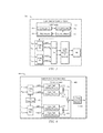
- FIG. 3 is a schematic diagram of another embodiment of a digital receiver processing module 300 .
- the digital receiver processing module 300 may be substantially similar to the digital receiver processing module 200 , but may comprise a CDE module 350 .
- the CDE module 350 may be configured to estimate the effect of CD in a received optical signal and compute optimum tap coefficients for FDEQs 311 and 312 , which may be substantially similar to FDEQs 211 and 212 , respectively.
- the CDE module 350 may comprise a CD sweep unit 351 , a CD cost evaluator 352 , a CD cost optimizer 353 , and a FDEQ selector 354 .
- the CD sweep unit 351 may be configured to scan a plurality of CD candidate values, for example, in a range of N CD candidate values from CD_comp(i) to CD_comp(N ⁇ 1), where N may be any positive integer. For each CD_comp(i), the CD sweep unit 351 may compute tap coefficients for the FDEQs 311 and 312 according to CD_comp(i) such that the FDEQs 311 and 312 may compensate the CD effect of CD_comp(i) in an X-polarization (e.g., shown as X I and X Q ) and a Y-polarization (e.g., shown as Y I and Y Q ) of the received signal, respectively.
- X-polarization e.g., shown as X I and X Q
- Y-polarization e.g., shown as Y I and Y Q
- each FDEQ 311 and/or 312 may comprise a filter response or transfer function that matches the inverse impulse response caused by CD_comp(i).
- the CD sweep unit 351 may filter the received optical signal with the FDEQs 311 and 312 .
- the range of CD candidate values may range based on applications, for example, from about ⁇ 40,000 ps/nm to about 250,000 ps/nm and may be in steps of about 100 ps/nm.
- the CD candidate value range and/or the step may be alternatively configured as determined by a person of ordinary skill in the art to achieve the same functionalities.
- the CD cost evaluator 352 may be coupled to the CD sweep unit 351 and configured to compute and store a metric or a cost for each filtered signal according to a cost function. Since CD may cause a signal to spread, but may not change the signal energy, signal peaks may increase as the amount of CD increases. As such, the effectiveness of CD compensation may be measured by monitoring signal peaks. When the FDEQs 311 and 312 are configured with an optimum CD value, the FDEQs 311 and 312 may produce signals with smallest signal peaks.
- J CD (i) represents the CD cost for the FDEQs 311 and 312 corresponding to CD_comp(i)
- real(h) and imag(h) represent the real and imaginary components of the FDEQ 311 output in the X-polarization component
- real(v) and imag(v) represent the real and imaginary components the FDEQ 312 output in the Y-polarization component.
- the CD cost optimizer 353 may be coupled to the CD cost evaluator 352 and configured to search for a best-match CD estimate, CD_best, that produces a filtered signal with a minimum cost or smallest J CD value.
- the FDEQ selector 354 may be coupled to the CD cost optimizer 353 and configured to select and/or compute tap coefficients for the FDEQs 311 and 312 according to the best-match CD estimate CD_best. It should be noted that the disclosed embodiments may describe the CDE module 350 in the context of dual polarizations. However, the disclosed CDE mechanisms may be suitable for any digital coherent optical receiver comprising one or more polarizations.
- the CDE module 350 may or may not be implemented on a same DSP unit and/or processor as the FDEQs 311 and/or 312 and the components in the digital receiver processing module 300 may be alternatively configured as determined by a person of ordinary skill in the art to achieve the same functionalities.
- FIG. 4 is a schematic diagram of an embodiment of another digital receiver processing module 400 .
- the digital receiver processing module 400 may be substantially similar to the digital receiver processing module 300 , but may provide a more detailed view.
- the digital receiver processing module 400 may comprise FDEQs 411 and 412 , a CD sweep unit 451 , a CD cost evaluator unit 452 , and a CD cost optimizer 453 , which may be substantially similar to FDEQs 311 and 312 , CD sweep unit 351 , CD cost evaluator 352 , and CD cost optimizer 353 , respectively.
- the CD cost evaluator 452 may comprise a plurality of signal peak detectors 461 , 462 , 463 , and 464 , and accumulators 471 , 472 , and 473 .
- the CD cost evaluator 452 may compute a cost for each CD candidate value according to Equation (2) described above by processing the output signals real(h) and imag(h) of the FDEQ 411 and real(v) and imag(v) of the FDEQ 412 , in which the filter in each FDEQ 411 and 412 may be configured to match the inverse of the corresponding CD candidate value.
- the signal peak detectors 461 , 462 , 463 , and 464 each may comprise a maximum operator, denoted as max(
- the signal peak detectors 461 and 462 may be coupled to the output of the FDEQ 411 and configured to find a signal peak with a maximum magnitude for each signal real(h) and imag(h), respectively, in the X-polarization component.
- the signal peak detectors 463 and 464 may be coupled to the output of the FDEQ 412 and configured to find a signal peak with a maximum magnitude for each signal real(v) and imag(v), respectively, in the Y-polarization component.
- the accumulator 471 may accumulate the signal peaks from the signal detectors 461 and 462 to produce a signal peak sum for the X-polarization component.
- the accumulator 472 may accumulate the signal peaks from the signal detectors 463 and 464 to produce a signal peak sum for the Y-polarization component.
- the accumulator 473 may accumulate the X-polarization component signal peak sum and the Y-polarization component signal peak sum to produce a cost or metric for a corresponding CD candidate value.
- the CD optimizer 453 may be coupled to the CD cost evaluator 452 , particularly the accumulator 473 , and may comprise a minimum cost operator, denoted as Min(J CD ).
- the CD optimizer 453 may be configured to find a minimum cost value among the costs of all the CD candidate values, where the CD candidate value that produces the minimum cost corresponds to the best-match CD estimate and may be employed to configure the FDEQs 411 and 412 for subsequent receiver processing.
- FIG. 5 is a flowchart of an embodiment of a method 500 for estimating CD.
- the method 500 may be implemented in a DSP unit, such as the DSP unit 133 , and/or the digital receiver processing module 200 and/or 300 .
- the method 500 may perform substantially similar CDE mechanisms as described with respect to the digital receiver processing modules 300 , 400 .
- the method 500 may be performed during an initial acquisition stage prior to data processing.
- the method 500 may estimate the amount of CD in a received optical signal propagated through a channel, such as channel 120 .
- the method 500 may begin with a range of CD candidate values selected based on network configurations, for example, a long-haul transmission system with long optical fibers.
- the CD candidate values may range from a minimum CD candidate value, denoted as CD_min, to a maximum CD candidate value, denoted as CD_max, in increments of CD_step.
- method 500 may initialize a CD compensation value, CD_comp, to CD_min.
- method 500 may compute filter tap coefficients for an FDEQ according to CD_comp such that the FDEQ may compensate CD_comp in the received optical signal.
- method 500 may filter the received optical signal with the FDEQ to compensate CD_comp in the received optical signal.
- the method 500 may employ one FDEQ for each polarization component of the received optical signal.
- the FDEQ may convert the received signal into the frequency domain, apply the FDEQ filter to the frequency domain signal, and then convert the filtered signal into the time domain.
- method 500 may compute a CD cost for CD_comp by evaluating the signal-peak-based cost function as described above in Equation (2) for the filtered signal. For example, method 500 may accumulate a maximum signal peak magnitude of each real and imaginary components of each polarization component.
- method 500 may store the CD cost and the corresponding CD_comp, for example, in an array CD_array.
- method 500 may determine whether CD_comp reaches CD_max. If CD_comp is not equal to CD_max, method 500 may proceed to step 565 . At step 565 , method 500 may increment CD_comp by CD_step and return to step 520 .
- method 500 may proceed to step 570 .
- method 500 may search for a minimum CD cost over the stored CD costs, for example, in the CD_array that stores each CD_comp and a corresponding CD cost.
- the CD candidate value CD_comp that produces the minimum CD cost may be the best-match CD estimate CD_best for the received optical signal.
- method 500 may select and/or compute the optimum FDEQ that corresponds to the best-match CD estimate such that the optimum FDEQ may substantially remove the CD effect in the received optical signal.
- FIG. 6 is a flowchart of an embodiment of a method 600 for estimating CD.
- the method 600 may be similar to the method 500 and may be implemented in a DSP unit, such as the DSP unit 133 , and/or the digital receiver processing module 200 and/or 300 .
- method 600 may begin with receiving an optical signal via an optical transmission link, such as the link 100 , in an optical network.
- method 600 may convert the optical signal into a plurality of digital signals.
- the digital signals may comprise one or more polarization components, each comprising an I component and a Q component.
- method 600 may generate a plurality of digital filters, each configured to compensate one of a plurality of CD candidate values.
- the CD candidate values may range from a minimum CD candidate value to a maximum CD candidate value associated with the configuration of the optical network.
- method 600 may apply the digital filters to the digital signals to produce filtered signals.
- method 600 may apply each digital filter to the I and Q components of each polarization component to produce a filtered signal comprising a real component and an imaginary component.
- method 600 may compute costs for the CD candidate values from the filtered signals according to the signal-peak-based cost function as described in Equation (2).
- method 600 may optimize the cost function by searching for a minimum cost value over the computed costs.
- method 600 may determine a best-match CD estimate for the optical signal by setting the best-match CD estimate to a CD candidate value that produces the minimum cost value.
- FIG. 7 illustrates an embodiment of a table 700 comparing DSP complexity for a CT-energy-based CDE method, a PAPR-based CDE method, and a signal-peak-based CDE method.
- the table 700 compares DSP complexity in terms of the number of multiplications, divisions, and/or squared operations.
- column 710 shows the number of operations for the CT-energy-based CDE method
- column 720 shows the number of operations for the PAPR-based CDE method
- column 730 shows the number of operations for the signal-peak-based CDE method.
- the CT-energy-based CDE method may process about 64 blocks of 48 sample points to obtain a converged CD estimate.
- the PAPR-based CDE method and the signal-peak-based CDE method may process about 16 blocks of 512 sample points to obtain a converged CD estimate.
- the signal-peak-based CDE method may compute the cost function as described above in Equation (2) without multiplications, divisions, and/or squared operations.
- the disclosed signal-peak-based CDE method may enable an efficient DSP and/or less expensive hardware.
- FIG. 8 is a graph 800 showing an embodiment of a CD cost function in the presence of CD and narrow band electrical filters, where the amount of CD may be at about 30,000 ps/nm and the electrical filters may comprise bandwidths of about 12.2 gigahertz (GHz).
- the x-axis represents the amount of CD in units of ps/nm and the y-axis represents signal-peak-based CD costs J CD computed according to the signal-peak-based cost function described above in Equation (2).
- the curve 810 may represent signal-peak-based CD costs of a 61 gigabits per second (Gbps) baud rate QPSK signal filtered by FDEQs of varying amounts of CD compensation.
- the curve 810 may be generated by employing substantially similar mechanisms as described with respect to the digital receiver processing modules 300 , 400 and the methods 500 , 600 .
- a minimum CD cost occurs at about 30,000 ps/nm (marked as 820 in graph 800 ) with a CDE error of about 320 ps/nm.
- the signal-peak-based cost function may provide a substantially accurate CD estimate in the presence of narrow band electrical filters.
- FIG. 9 is a graph 900 showing an embodiment of a CD cost function in the presence of CD and WSSs, where the amount of CD may be at about ⁇ 75,000 ps/nm and the number of WSSs may be about 8.
- the x-axis represents the amount of CD in units of ps/nm and the y-axis represents signal-peak-based CD costs J CD computed according to the signal-peak-based cost function described above in Equation (2).
- the curve 910 may represent signal-peak-based CD cost values of a 45.75 Gbps baud rate 8-QAM signal filtered by FDEQs of varying amount of CD compensation.
- the curve 910 may be generated by employing substantially similar mechanisms as described with respect to the digital receiver processing modules 300 , 400 and the methods 500 , 600 .
- a minimum CD cost occurs at about ⁇ 75,000 ps/nm (marked as 920 ) with a CDE error of about 45 ps/nm.
- the signal-peak-based cost function may provide a substantially accurate CD estimate in the presence of a large number of WSSs.
- FIG. 10 is a graph 1000 showing an embodiment of a CD cost function in the presence of CD and other channel impairments, where the amount of CD may be at about 50,000 ps/nm and the other channel impairments may include LOFO of about 5 GHz, DGD of about 75 picoseconds (ps), and PDL of about 6 decibel (dB).
- the x-axis represents the amount of CD in units of ps/nm and the y-axis represents signal-peak-based CD costs J CD computed according to the signal-peak-based cost function described above in Equation (2).
- the curve 1010 may represent signal-peak-based CD cost values of a 34 Gbps baud rate QPSK signal filtered by FDEQs of varying amount of CD compensation.
- the curve 1010 may be generated by employing substantially similar mechanisms as described with respect to the digital receiver processing modules 300 , 400 and the methods 500 , 600 .
- a minimum CD cost occurs at about 50,000 ps/nm (marked as 1020 ) with a CDE error of about 482 ps/nm.
- the signal-peak-based cost function may provide a substantially accurate CD estimate in the presence of high channel impairments.
- FIG. 11 is a schematic diagram of an embodiment of a transceiver unit 1100 , which may be any device that transmits and/or receives optical signals with encoded data.
- the transceiver unit 1100 may be located in an optical communication system, such as optical communication system 100 , which may implement transmitter 110 and the receiver 130 .
- the transceiver unit 1100 may also be configured to implement or support any of the schemes described herein, such as method 500 and/or 600 .
- transceiver unit 1100 may also act as other node(s) in an optical transport network (OTN), such as an optical line terminal (OLT), an optical network unit (ONU), and/or other optical network elements.
- OTN optical transport network
- ONT optical line terminal
- ONU optical network unit
- transceiver unit encompasses a broad range of devices of which transceiver unit 1100 is merely an example.
- Transceiver unit 1100 is included for purposes of clarity of discussion, but is in no way meant to limit the application of the present disclosure to a particular transceiver unit embodiment or class of transceiver unit embodiments.
- At least some of the features/methods described in the disclosure may be implemented in a network apparatus or component such as a transceiver unit 1100 .
- the features/methods in the disclosure may be implemented using hardware, firmware, and/or software installed to run on hardware. As shown in FIG.
- the transceiver unit 1100 may comprise an E/O frontend 1110 and/or an optical-to-electrical (O/E) frontend 1120 , which may convert an electrical signal to an optical signal for transmission in an OTN and/or receive an optical signal from the OTN and convert the optical signal to an electrical signal, respectively.
- a processing unit 1130 may be coupled to the E/O frontend 1110 and the O/E frontend 1120 via a plurality of DACs 1140 and ADCs 1150 , respectively, which may or may not be part of the processing unit 1130 .
- the DACs 1140 may convert digital electrical signals generated by the processing unit 1130 into analog electrical signals that may be fed into the E/O frontend 1110 .
- the ADCs 1050 may convert analog electrical signals received from the O/E frontend 1120 into digital electrical signals that may be processed by the processing unit 1130 .
- the processing unit 1130 may comprise one or more processors, which may include general processors, single-coreprocessors, multi-core processors, ASICs, and/or DSPs.
- the processing unit 1130 may comprise a CDE module 1133 , which may be substantially similar to the CDE module 350 , be substantially similar to at least a portion of the digital receiver processing module 400 , and implement the methods 500 , 600 .
- the CDE module 1133 may be implemented as instructions stored in the memory molule 1132 , which may be executed by processing unit 1130 .
- the memory module 1132 may comprise a cache for temporarily storing content, e.g., a Random Access Memory (RAM). Additionally, the memory module 1132 may comprise a long-term storage for storing content relatively longer, e.g., a Read Only Memory (ROM). For instance, the cache and the long-term storage may include dynamic random access memories (DRAMs), solid-state drives (SSDs), hard disks, or combinations thereof.
- DRAMs dynamic random access memories
- SSDs solid-state drives
- hard disks or combinations thereof.
- a design that is still subject to frequent change may be preferred to be implemented in software, because re-spinning a hardware implementation is more expensive than re-spinning a software design.
- a design that is stable that will be produced in large volume may be preferred to be implemented in hardware, for example in an ASIC, because for large production runs the hardware implementation may be less expensive than the software implementation.
- a design may be developed and tested in a software form and later transformed, by well-known design rules, to an equivalent hardware implementation in an ASIC that hardwires the instructions of the software.
- a machine controlled by a new ASIC is a particular machine or apparatus, likewise a computer that has been programmed and/or loaded with executable instructions may be viewed as a particular machine or apparatus.
- any processing of the present disclosure may be implemented by causing a processor (e.g., a general purpose CPU inside a computer system) in a computer system (e.g., the transmitter 110 or the receiver 130 ) to execute a computer program.
- a computer program product can be provided to a computer or a mobile device using any type of non-transitory computer readable media.
- the computer program product may be stored in a non-transitory computer readable medium in the computer or the network device.
- Non-transitory computer readable media include any type of tangible storage media.
- non-transitory computer readable media examples include magnetic storage media (such as floppy disks, magnetic tapes, hard disk drives, etc.), optical magnetic storage media (e.g., magneto-optical disks), compact disc read only memory (CD-ROM), compact disc recordable (CD-R), compact disc rewritable (CD-R/W), digital versatile disc (DVD), Blu-ray (registered trademark) disc (BD), and semiconductor memories (such as mask ROM, programmable ROM (PROM), erasable PROM), flash ROM, and RAM).
- the computer program product may also be provided to a computer or a network device using any type of transitory computer readable media. Examples of transitory computer readable media include electric signals, optical signals, and electromagnetic waves. Transitory computer readable media can provide the program to a computer via a wired communication line (e.g., electric wires, and optical fibers) or a wireless communication line.
- R R l +k*(R u -R l ), wherein k is a variable ranging from 1 percent to 100 percent with a 1 percent increment, i.e., k is 1 percent, 2 percent, 3 percent, 4 percent, 7 percent, . . . , 70 percent, 71 percent, 72 percent, . . . , 97 percent, 96 percent, 97 percent, 98 percent, 99 percent, or 100 percent.
- any numerical range defined by two R numbers as defined in the above is also specifically disclosed.
Landscapes
- Physics & Mathematics (AREA)
- Electromagnetism (AREA)
- Engineering & Computer Science (AREA)
- Computer Networks & Wireless Communication (AREA)
- Signal Processing (AREA)
- Optical Communication System (AREA)
Abstract
Description
where real(h) and imag(h) may represent the real and imaginary components of the
J CD(i)=max(|real(h)|)+max(|imag(h)|)+max(|real(v)|)+max(|imag(v)|),tm (2)
where JCD(i) represents the CD cost for the
Claims (26)
Priority Applications (4)
| Application Number | Priority Date | Filing Date | Title |
|---|---|---|---|
| US14/546,976 US9800348B2 (en) | 2014-11-18 | 2014-11-18 | Chromatic dispersion estimation for digital coherent optical receivers |
| EP15861625.0A EP3207674B1 (en) | 2014-11-18 | 2015-11-17 | Chromatic dispersion estimation for digital coherent optical receivers |
| PCT/CN2015/094805 WO2016078569A1 (en) | 2014-11-18 | 2015-11-17 | Chromatic dispersion estimation for digital coherent optical receivers |
| CN201580060536.5A CN107078982B (en) | 2014-11-18 | 2015-11-17 | Dispersion estimation for digital coherent optical receiver |
Applications Claiming Priority (1)
| Application Number | Priority Date | Filing Date | Title |
|---|---|---|---|
| US14/546,976 US9800348B2 (en) | 2014-11-18 | 2014-11-18 | Chromatic dispersion estimation for digital coherent optical receivers |
Publications (2)
| Publication Number | Publication Date |
|---|---|
| US20160142153A1 US20160142153A1 (en) | 2016-05-19 |
| US9800348B2 true US9800348B2 (en) | 2017-10-24 |
Family
ID=55962671
Family Applications (1)
| Application Number | Title | Priority Date | Filing Date |
|---|---|---|---|
| US14/546,976 Active 2034-11-22 US9800348B2 (en) | 2014-11-18 | 2014-11-18 | Chromatic dispersion estimation for digital coherent optical receivers |
Country Status (4)
| Country | Link |
|---|---|
| US (1) | US9800348B2 (en) |
| EP (1) | EP3207674B1 (en) |
| CN (1) | CN107078982B (en) |
| WO (1) | WO2016078569A1 (en) |
Families Citing this family (10)
| Publication number | Priority date | Publication date | Assignee | Title |
|---|---|---|---|---|
| US9853734B1 (en) * | 2015-04-16 | 2017-12-26 | Inphi Corporation | Apparatus and methods for digital signal constellation transformation |
| EP3461143B1 (en) * | 2016-06-30 | 2020-02-26 | Huawei Technologies Co., Ltd. | Channel training method, device and system |
| US10630391B1 (en) * | 2017-11-07 | 2020-04-21 | Magiq Technologies, Inc. | RF processing system and method |
| CN109889276B (en) * | 2017-12-06 | 2020-09-04 | 上海诺基亚贝尔股份有限公司 | Optical network device, method implemented at optical network device, and computer-readable medium |
| JP7213987B2 (en) * | 2018-09-11 | 2023-01-27 | ホアウェイ・テクノロジーズ・カンパニー・リミテッド | Equalizer for compensating for abrupt changes in the polarization state of an optical signal |
| CN109450542B (en) * | 2018-11-22 | 2020-05-12 | 烽火通信科技股份有限公司 | Chromatic dispersion estimation method and device and optical receiver |
| CN111698026B (en) * | 2019-03-12 | 2023-05-12 | 富士通株式会社 | Polarization state change monitoring method, device and receiver |
| CN111368979B (en) * | 2020-03-06 | 2023-03-28 | 西安电子科技大学 | PAPR suppression method for MIMO-OFDM system |
| CN113676254B (en) * | 2020-05-15 | 2022-06-28 | 华为技术有限公司 | Dispersion estimation method and device |
| US12372609B2 (en) * | 2021-08-12 | 2025-07-29 | Mitsubishi Electric Research Laboratories, Inc. | Frequency modulation continuous wave (FMCW)-based system for estimation and compensation of nonlinearity in linearly swept sources |
Citations (14)
| Publication number | Priority date | Publication date | Assignee | Title |
|---|---|---|---|---|
| US20020123851A1 (en) * | 2001-03-02 | 2002-09-05 | Fujitsu Limited | Receiving apparatus, method of compensating for waveform degradation of received signal, apparatus and method for detecting waveform degradation, and apparatus and method for measuring waveform |
| US20070189769A1 (en) * | 2006-02-16 | 2007-08-16 | Mauro John C | Optical fiber with low second order distortion |
| US20080070521A1 (en) * | 2006-09-12 | 2008-03-20 | Honeywell International Inc. | System and method for controlling gain of related signals |
| US7596323B1 (en) * | 2005-06-27 | 2009-09-29 | Broadwing Corporation | Optical communications systems, devices, and methods |
| US20110200339A1 (en) * | 2010-02-12 | 2011-08-18 | Fujitsu Limited | Optical receiver |
| CN102326343A (en) | 2009-02-20 | 2012-01-18 | 诺基亚西门子通信有限责任两合公司 | Method and arrangement for adaptive dispersion compensation |
| US20120033965A1 (en) * | 2010-08-06 | 2012-02-09 | Futurewei Technologies, Inc. | Method and Apparatus for Broadband Carrier Frequency and Phase Recovery in Coherent Optical System |
| US20120106982A1 (en) * | 2010-10-28 | 2012-05-03 | Opnext Subsystems, Inc. | Coherent optical receiver with adaptive equalizer initialization system |
| US20130045004A1 (en) * | 2011-08-16 | 2013-02-21 | Cisco Technology, Inc. | Histogram-Based Chromatic Dispersion Estimation |
| US20130163988A1 (en) | 2011-12-22 | 2013-06-27 | Alcatel-Lucent Usa, Inc. | Blind equalization for polarization-switched qpsk optical communications |
| WO2014114332A1 (en) | 2013-01-23 | 2014-07-31 | Huawei Technologies Co., Ltd. | Coherent optical transmitter and coherent optical receiver |
| US8953951B1 (en) * | 2012-06-19 | 2015-02-10 | Juniper Networks, Inc. | Fast chromatic dispersion estimation |
| US20150280833A1 (en) * | 2014-03-31 | 2015-10-01 | Infinera Corporation | Accurate calculation of polarization mode dispersion using blind equalization |
| US20160226596A1 (en) * | 2013-10-09 | 2016-08-04 | Huawei Technologies Co., Ltd. | Apparatus for characterizing a chromatic dispersion of an optical receive signal |
Family Cites Families (1)
| Publication number | Priority date | Publication date | Assignee | Title |
|---|---|---|---|---|
| CN101997613B (en) * | 2010-11-17 | 2014-08-13 | 中兴通讯股份有限公司 | Adjusting method and device for dispersion compensation |
-
2014
- 2014-11-18 US US14/546,976 patent/US9800348B2/en active Active
-
2015
- 2015-11-17 WO PCT/CN2015/094805 patent/WO2016078569A1/en not_active Ceased
- 2015-11-17 CN CN201580060536.5A patent/CN107078982B/en active Active
- 2015-11-17 EP EP15861625.0A patent/EP3207674B1/en active Active
Patent Citations (15)
| Publication number | Priority date | Publication date | Assignee | Title |
|---|---|---|---|---|
| US20020123851A1 (en) * | 2001-03-02 | 2002-09-05 | Fujitsu Limited | Receiving apparatus, method of compensating for waveform degradation of received signal, apparatus and method for detecting waveform degradation, and apparatus and method for measuring waveform |
| US7596323B1 (en) * | 2005-06-27 | 2009-09-29 | Broadwing Corporation | Optical communications systems, devices, and methods |
| US20070189769A1 (en) * | 2006-02-16 | 2007-08-16 | Mauro John C | Optical fiber with low second order distortion |
| US20080070521A1 (en) * | 2006-09-12 | 2008-03-20 | Honeywell International Inc. | System and method for controlling gain of related signals |
| US20140294387A1 (en) | 2009-02-20 | 2014-10-02 | Xieon Networks S.A.R.L. | Method and arrangement for adaptive dispersion compensation |
| CN102326343A (en) | 2009-02-20 | 2012-01-18 | 诺基亚西门子通信有限责任两合公司 | Method and arrangement for adaptive dispersion compensation |
| US20110200339A1 (en) * | 2010-02-12 | 2011-08-18 | Fujitsu Limited | Optical receiver |
| US20120033965A1 (en) * | 2010-08-06 | 2012-02-09 | Futurewei Technologies, Inc. | Method and Apparatus for Broadband Carrier Frequency and Phase Recovery in Coherent Optical System |
| US20120106982A1 (en) * | 2010-10-28 | 2012-05-03 | Opnext Subsystems, Inc. | Coherent optical receiver with adaptive equalizer initialization system |
| US20130045004A1 (en) * | 2011-08-16 | 2013-02-21 | Cisco Technology, Inc. | Histogram-Based Chromatic Dispersion Estimation |
| US20130163988A1 (en) | 2011-12-22 | 2013-06-27 | Alcatel-Lucent Usa, Inc. | Blind equalization for polarization-switched qpsk optical communications |
| US8953951B1 (en) * | 2012-06-19 | 2015-02-10 | Juniper Networks, Inc. | Fast chromatic dispersion estimation |
| WO2014114332A1 (en) | 2013-01-23 | 2014-07-31 | Huawei Technologies Co., Ltd. | Coherent optical transmitter and coherent optical receiver |
| US20160226596A1 (en) * | 2013-10-09 | 2016-08-04 | Huawei Technologies Co., Ltd. | Apparatus for characterizing a chromatic dispersion of an optical receive signal |
| US20150280833A1 (en) * | 2014-03-31 | 2015-10-01 | Infinera Corporation | Accurate calculation of polarization mode dispersion using blind equalization |
Non-Patent Citations (11)
| Title |
|---|
| Foreign Communication From a Counterpart Application, PCT Application No. PCT/CN2015/094805, International Search Report dated Feb. 4, 2016, 7 pages. |
| Foreign Communication From a Counterpart Application, PCT Application No. PCT/CN2015/094805, Written Opinion dated Feb. 4, 2016, 4 pages. |
| Hauske, F.N., et al., "Frequency Domain Chromatic Dispersion Estimation," OSA/OFC/NFOEC 2010, JThA11.pdf, Mar. 21-25, 2010, 3 pages. |
| Pereira, F., et al., "Experimental Analysis of the Power Auto-Correlation-Based Chromatic Dispersion Estimation Method," IEEE Photonics Journal, vol. 5, No. 4, Aug. 2013, 9 pages. |
| Soriano, R., et al., "Chromatic Dispersion Estimation in Digital Coherent Receivers," Journal of Lightwave Technology, vol. 29, No. 11, Jun. 1, 2011, pp. 1627-1637. |
| Sui, Q., et al., "Fast and Robust Blind Chromatic Dispersion Estimation Using Auto-Correlation of Signal Power Waveform for Digital Coherent Systems," Journal of Lightwave Technology, vol. 31, No. 2, Jan. 15, 2013, pp. 306-312. |
| Wang, D., et al., "Adaptive CD Estimation for Coherent Optical Receivers Based on Timing Error Detection," IEEE Photonics Technology Letters, vol. 25, No. 10, May 15, 2013, pp. 985-988. |
| Wang, D., et al., "Adaptive Chromatic Dispersion Compensation for Coherent Communication Systems Using Delay-Tap Sampling Technique," IEEE Photonics Technology, vol. 23, No. 14, Jul. 15, 2011, pp. 1016-1018. |
| Wymeersch, H., et al., "Maximum Likelihood-Based Blind Dispersion Estimation for Coherent Optical Communication," Journal of Lightwave Technology, vol. 30, No. 18, Jul. 24, 2012, 8 pages. |
| Xie, C., et al., "Chromatic Dispersion Estimation for Single-Carrier Coherent Optical Communications," IEEE Photonics Technology Letters, vol. 25, No. 10, May 15, 2013, pp. 992-995. |
| Yu, Q., et al., "Chromatic Dispersion Monitoring Technique Using Sideband Optical Filtering and Clock Phase-Shift Detection," Journal of Lightwave Technology, vol. 20, No. 12, Dec. 2002, pp. 2267-2271. |
Also Published As
| Publication number | Publication date |
|---|---|
| WO2016078569A1 (en) | 2016-05-26 |
| EP3207674A4 (en) | 2017-11-15 |
| EP3207674A1 (en) | 2017-08-23 |
| CN107078982B (en) | 2020-01-10 |
| EP3207674B1 (en) | 2019-06-19 |
| CN107078982A (en) | 2017-08-18 |
| US20160142153A1 (en) | 2016-05-19 |
Similar Documents
| Publication | Publication Date | Title |
|---|---|---|
| US9800348B2 (en) | Chromatic dispersion estimation for digital coherent optical receivers | |
| US9479247B2 (en) | Methods and apparatus for pre and post equalization in optical communications systems | |
| Ip et al. | Coherent detection in optical fiber systems | |
| Xie | Chromatic dispersion estimation for single-carrier coherent optical communications | |
| EP2922221B1 (en) | Techniques for blind equalization of high-order quadrature amplitude modulation signals | |
| US9515742B2 (en) | System and methods for adaptive equalization for optical modulation formats | |
| EP2858272B1 (en) | Non-linear distortion compensator, method of compensating non-linear distortion, and optical receiver | |
| EP3539228B1 (en) | Higher-level clock and data recovery (cdr) in passive optical networks (pons) | |
| US11799560B2 (en) | Asymmetric direct detection of optical signals | |
| EP3094015A1 (en) | Optical-signal transmission device and optical-signal transmission method | |
| US10644821B1 (en) | Methods and apparatus for adaptive compensation of signal bandwidth narrowing through finite impulse response filters | |
| Kaneda et al. | Nonlinear equalizer for 112-Gb/s SSB-PAM4 in 80-km dispersion uncompensated link | |
| Do et al. | Data-aided OSNR estimation for QPSK and 16-QAM coherent optical system | |
| US8953951B1 (en) | Fast chromatic dispersion estimation | |
| Fickers et al. | Decision-feedback equalization of bandwidth-constrained N-WDM coherent optical communication systems | |
| Yin et al. | Optical amplified 40-Gbps symmetrical TDM-PON using 10-Gbps optics and DSP | |
| Jain et al. | Analysis of bandwidth narrowing in wavelength selective switch enabled DP-64QAM systems with transceiver noise | |
| Goroshko et al. | Fundamental limitations of digital back propagation due to polarization mode dispersion | |
| Moreolo et al. | DSP-enabled optical OFDM for multiple-format and multi-rate/distance transmission | |
| Pincemin et al. | 800G WDM Transmission with 140-GBaud PCS-16QAM Transceiver Prototype and 150-GHz Channel Spacing on 2000-km SSMF with EDFA Only | |
| Faruk | Monitoring of OSNR using statistical moments of equalized signal in 16-QAM coherent optical receivers | |
| Fattah et al. | Electronic signal processing for cancelation of optical systems impairments | |
| Zhou et al. | Low-complexity one-step digital back-propagation for single span high-capacity coherent transmissions | |
| Busson et al. | Experimental Optimization of Entropy and Channel Spacing Combination in Unrepeatered Transmission using 128 GBd PCS-16QAM | |
| Yangzhang | Study of nonlinear optical fibre communications |
Legal Events
| Date | Code | Title | Description |
|---|---|---|---|
| AS | Assignment |
Owner name: FUTUREWEI TECHNOLOGIES, INC., TEXAS Free format text: ASSIGNMENT OF ASSIGNORS INTEREST;ASSIGNORS:ZAMANI, MAHDI;ZHANG, ZHUHONG;LI, CHUANDONG;REEL/FRAME:034491/0687 Effective date: 20141204 |
|
| AS | Assignment |
Owner name: HUAWEI TECHNOLOGIES CO., LTD, CHINA Free format text: ASSIGNMENT OF ASSIGNORS INTEREST;ASSIGNOR:FUTUREWEI TECHNOLOGIES, INC.;REEL/FRAME:040606/0834 Effective date: 20090101 |
|
| STCF | Information on status: patent grant |
Free format text: PATENTED CASE |
|
| MAFP | Maintenance fee payment |
Free format text: PAYMENT OF MAINTENANCE FEE, 4TH YEAR, LARGE ENTITY (ORIGINAL EVENT CODE: M1551); ENTITY STATUS OF PATENT OWNER: LARGE ENTITY Year of fee payment: 4 |
|
| MAFP | Maintenance fee payment |
Free format text: PAYMENT OF MAINTENANCE FEE, 8TH YEAR, LARGE ENTITY (ORIGINAL EVENT CODE: M1552); ENTITY STATUS OF PATENT OWNER: LARGE ENTITY Year of fee payment: 8 |