US9800244B2 - Inverter circuits with first and second drivability dependent on first or second time period - Google Patents
Inverter circuits with first and second drivability dependent on first or second time period Download PDFInfo
- Publication number
- US9800244B2 US9800244B2 US15/086,669 US201615086669A US9800244B2 US 9800244 B2 US9800244 B2 US 9800244B2 US 201615086669 A US201615086669 A US 201615086669A US 9800244 B2 US9800244 B2 US 9800244B2
- Authority
- US
- United States
- Prior art keywords
- drive
- pull
- output signal
- time period
- signal
- Prior art date
- Legal status (The legal status is an assumption and is not a legal conclusion. Google has not performed a legal analysis and makes no representation as to the accuracy of the status listed.)
- Active
Links
Images


Classifications
-
- H—ELECTRICITY
- H03—ELECTRONIC CIRCUITRY
- H03K—PULSE TECHNIQUE
- H03K19/00—Logic circuits, i.e. having at least two inputs acting on one output; Inverting circuits
- H03K19/003—Modifications for increasing the reliability for protection
- H03K19/00369—Modifications for compensating variations of temperature, supply voltage or other physical parameters
- H03K19/00384—Modifications for compensating variations of temperature, supply voltage or other physical parameters in field effect transistor circuits
-
- H—ELECTRICITY
- H03—ELECTRONIC CIRCUITRY
- H03K—PULSE TECHNIQUE
- H03K19/00—Logic circuits, i.e. having at least two inputs acting on one output; Inverting circuits
- H03K19/20—Logic circuits, i.e. having at least two inputs acting on one output; Inverting circuits characterised by logic function, e.g. AND, OR, NOR, NOT circuits
-
- H—ELECTRICITY
- H03—ELECTRONIC CIRCUITRY
- H03K—PULSE TECHNIQUE
- H03K5/00—Manipulating of pulses not covered by one of the other main groups of this subclass
- H03K5/01—Shaping pulses
- H03K5/04—Shaping pulses by increasing duration; by decreasing duration
- H03K5/06—Shaping pulses by increasing duration; by decreasing duration by the use of delay lines or other analogue delay elements
Definitions
- Embodiments of the present disclosure may generally relate to inverter circuits.
- NBTI negative bias temperature instability
- the NBTI phenomenon means that a threshold voltage (an absolute value) of a PMOS transistor increases to reduce an on-current and a switching speed of the PMOS transistor after the PMOS transistor is turned on for a long time. That is, if the PMOS transistor is exposed to a condition causing the NBTI phenomenon, operation timing of the PMOS transistor may change. This may lead to timing errors of internal circuits of the semiconductor device. These timing errors may cause degradation of the performance and reliability of the semiconductor device.
- an inverter circuit may include a pull-up control circuit and a pull-up drive circuit.
- the pull-up control circuit may generate a drive signal which may be enabled during a first time period based on an input signal and an output signal.
- the pull-up drive circuit may drive the output signal to a power supply voltage based on the input signal and the drive signal.
- the pull-up drive circuit may drive the output signal with a first drivability during the first time period and may drive the output signal with a second drivability during a second time period.
- an inverter circuit may include a pull-up drive circuit and a pull-down drive circuit.
- the pull-up drive circuit may drive an output signal to a power supply voltage based on an input signal and a drive signal.
- the pull-down drive circuit may drive the output signal to a ground voltage based on the input signal.
- the pull-up drive circuit may drive the output signal with a first drivability during a first time period and may drive the output signal with a second drivability during a second time period.
- an inverter circuit may include a pull-up drive circuit.
- the pull-up drive circuit may drive an output signal to a power supply voltage based on an input signal and a drive signal.
- the pull-up drive circuit may use a first transistor to drive the output signal during a first time period and uses a second transistor to drive the output signal during a second time period after the first time period.
- the first transistor has a higher drivability than the second transistor
- the first transistor is only turned on during the first time period.
- the first transistor pulls up the output signal from a logic low level to a logic high level and the second transistor maintains the output signal at a logic high level for a pull-up operation.
- the first transistor includes a PMOS transistor different from a PMOS transistor included in the second transistor.
- the pull-up drive circuit uses the first transistor, the second transistor, and a third transistor to drive the output signal during the first time period and only uses the second transistor to drive the output signal during the second time period.
- the first, second, and third transistors have substantially the same drivability.
- the first, second, and third transistors are all simultaneously turned on during the first time period.
- the first transistor includes a PMOS transistor
- the second transistor includes a PMOS transistor
- third transistor includes a third transistor.
- the inverter circuit may further include a pull-up control circuit.
- the pull-up control circuit may generate the drive signal which is enabled during the first time period based on the input signal and the output signal.
- the inverter circuit may further include a pull-down drive circuit.
- the pull-down drive circuit may drive the output signal to a ground voltage based on the input signal.
- FIG. 1 is a block diagram illustrating a representation of an example of a configuration of an inverter circuit according to an embodiment.
- FIG. 2 is a circuit diagram illustrating a representation of an example of a pull-up control circuit included in the inverter circuit of FIG. 1 .
- FIG. 3 is a circuit diagram illustrating a representation of an example of a pull-up drive circuit included in the inverter circuit of FIG. 1 .
- FIG. 4 is a circuit diagram illustrating a representation of an example of the pull-up drive circuit included in the inverter circuit of FIG. 1 .
- FIG. 5 is a circuit diagram illustrating a representation of an example of a pull-down drive circuit included in the inverter circuit of FIG. 1 .
- FIG. 6 is a timing diagram illustrating a representation of an example of an operation of the inverter circuit illustrated in FIGS. 1 to 5 .
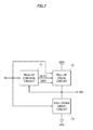
- FIG. 7 is a block diagram illustrating a representation of an example of a configuration of an inverter circuit according to an embodiment.
- FIG. 8 is a circuit diagram illustrating a representation of an example of a pull-up control circuit included in the inverter circuit of FIG. 7 .
- FIG. 9 is a circuit diagram illustrating a representation of an example of a pull-up drive circuit included in the inverter circuit of FIG. 7 .
- FIG. 10 illustrates a block diagram of an example of a representation of a system employing an inverter circuit with the various embodiments discussed above with relation to FIGS. 1-9 .
- an inverter circuit may include a pull-up control circuit 11 , a pull-up drive circuit 12 , and a pull-down drive circuit 13 .
- the pull-up control circuit 11 may generate a drive signal DRV which is enabled during a first time period in response to an input signal IN and an output signal OUT.
- the first time period may be set to start at a point of time that the input signal IN is changed from a logic high level into a logic low level and to terminate at a point of time that the output signal OUT is changed from a logic low level into a logic high level.
- the pull-up control circuit 11 may output the input signal IN having a logic low level as the drive signal DRV during the first time period. At a point of time that the first time period terminates, the pull-up control circuit 11 may stop an operation for outputting the input signal IN as the drive signal DRV and may drive the drive signal DRV to a logic high level to disable the drive signal DRV.
- the pull-up drive circuit 12 may drive the output signal OUT to a power supply voltage VDD in response to the input signal IN and the drive signal DRV.
- the pull-up drive circuit 12 may drive the output signal OUT with a first drivability during the first time period and may drive the output signal OUT with a second drivability during a second time period.
- the second time period may start at a point of time that the first time period terminates and may terminate at a point of time that the input signal IN is changed from a logic low level into a logic high level.
- the pull-down drive circuit 13 may drive the output signal OUT to a ground voltage VSS in response to the input signal IN.
- the pull-down drive circuit 13 may drive the output signal OUT to the ground voltage VSS during a time period that the input signal IN has a logic high level.
- the pull-up control circuit 11 may include a transfer circuit 21 , a drive termination control circuit 22 , and a drive control circuit 23 .
- the transfer circuit 21 may include an inverter IV 21 and a transfer gate T 21 .
- the inverter IV 21 may inversely buffer the output signal OUT and may output the inversely buffered signal of the output signal OUT.
- the transfer gate T 21 may output the input signal IN as the drive signal DRV in response to the output signal OUT.
- the transfer gate T 21 may output the input signal IN as the drive signal DRV during the first time period in response to the output signal OUT.
- the transfer circuit 21 may output the input signal IN having a logic low level as the drive signal DRV during the first time period.
- the drive signal DRV may be enabled if the drive signal DRV has a logic low level.
- the transfer circuit 21 may stop an operation for outputting the input signal IN as the drive signal DRV during the second time period that the output signal OUT has a logic high level.
- the drive termination control circuit 22 may include a delay circuit 221 and a logic circuit 222 .
- the delay circuit 221 may delay the output signal OUT by a predetermined time period to generate a delayed output signal OUTD.
- the logic circuit 222 may include a NOR gate NR 21 and an inverter IV 22 .
- the NOR gate NR 21 may perform a NOR operation of the input signal IN and the delayed output signal OUTD and may output a result of the NOR operation.
- the inverter IV 22 may inversely buffer an output signal of the NOR gate NR 21 to generate a drive termination signal DIS.
- the drive termination control circuit 22 may receive the input signal IN having a logic high level and the output signal OUT having a logic low level before the first time period to generate the drive termination signal DIS which is disabled to have a logic high level.
- the drive termination control circuit 22 may receive the input signal IN having a logic high level during the first time period to delay the input signal IN using the logic circuit 222 and to generate the drive termination signal DIS which is enabled during the second time period.
- the logic circuit 222 may change the number or the drivability of inverters included in the logic circuit 222 to adjust a point of time that the drive termination signal DIS is generated.
- the drive control circuit 23 may include a PMOS transistor P 21 .
- the drive control circuit 23 may disable the drive signal DRV in response to the drive termination signal DIS.
- the drive control circuit 23 may drive the drive signal DRV to the power supply voltage VDD to disable the drive signal DRV if the drive termination signal DIS is enabled.
- the pull-up drive circuit 12 may include PMOS transistors P 31 and P 32 .
- the PMOS transistors P 31 and P 32 may operate as pull-up elements which pull up the output signal OUT.
- the PMOS transistor P 31 may drive the output signal OUT to the power supply voltage VDD in response to the drive signal DRV.
- the PMOS transistor P 31 may drive the output signal OUT to the power supply voltage VDD in response to the drive signal DRV during the first time period.
- the PMOS transistor P 32 may drive the output signal OUT to the power supply voltage VDD in response to the input signal IN.
- the PMOS transistor P 32 may drive the output signal OUT to the power supply voltage VDD in response to the input signal IN having a logic low level during the first time period and the second time period.
- the PMOS transistor P 31 may have a drivability which is higher than that of the PMOS transistor P 32 .
- the PMOS transistors P 31 and P 32 may be simultaneously turned on during the first time period. Since the PMOS transistor P 31 has a drivability higher than that of the PMOS transistor P 32 , the output signal OUT may be driven to the power supply voltage VDD by the PMOS transistor P 31 during the first time period. Only the PMOS transistor P 32 may be turned on during the second time period. That is, the PMOS transistor P 32 may perform an operation for keeping the output signal OUT having the power supply voltage VDD during the second time period. Hence, the PMOS transistor P 31 may only drive the output signal OUT to the power supply voltage VDD, and the PMOS transistor P 32 may only keep the output signal OUT having the power supply voltage VDD.
- the pull-up drive circuit 12 may include PMOS transistors P 41 , P 42 , and P 43 .
- the PMOS transistors P 41 , P 42 , and P 43 may operate as pull-up elements which pull up the output signal OUT.
- the PMOS transistors P 41 and P 42 may drive the output signal OUT to the power supply voltage VDD in response to the drive signal DRV.
- the PMOS transistors P 41 and P 42 may drive the output signal OUT to the power supply voltage VDD in response to the drive signal DRV during the first time period.
- the PMOS transistor P 43 may drive the output signal OUT to the power supply voltage VDD in response to the input signal IN.
- the PMOS transistor P 43 may drive the output signal OUT to the power supply voltage VDD in response to the input signal IN having a logic low level during the first time period and the second time period. All of The PMOS transistors P 41 , P 42 , and P 43 may have the same drivability. The PMOS transistors P 41 , P 42 , and P 43 may be simultaneously turned on during the first time period. Since the PMOS transistors P 41 , P 42 , and P 43 are simultaneously turned on during the first time period, the output signal OUT may be quickly driven to the power supply voltage VDD by the PMOS transistors P 41 , P 42 , and P 43 which are turned on during the first time period. Only the PMOS transistor P 43 may be turned on during the second time period.
- the PMOS transistor P 43 may perform an operation for keeping the output signal OUT having the power supply voltage VDD during the second time period. Hence, the PMOS transistors P 41 , P 42 , and P 43 may simultaneously drive the output signal OUT to the power supply voltage VDD, and only the PMOS transistor P 43 may keep the output signal OUT having the power supply voltage VDD.
- the pull-down drive circuit 13 may include an NMOS transistor N 51 .
- the NMOS transistor N 51 may operate as a pull-down element which drives the output signal OUT to the ground voltage VSS.
- the NMOS transistor N 51 may drive the output signal OUT to the ground voltage VSS in response to the input signal IN.
- the drive signal DRV may be enabled to have a logic low level during a first time period TD 1 from a point of time T 1 to a point of time T 2 .
- the point of time T 1 may correspond to a point of time that the input signal IN is changed from a logic high level into a logic low level.
- the point of time T 2 may be set to be a point of time that the output signal OUT reaches a logic high level from a logic low level.
- the output signal OUT may be driven to the power supply voltage VDD by the PMOS transistor P 31 having a drivability which is higher than a drivability of the PMOS transistor P 32 .
- the drive signal DRV may be disabled to a logic high level.
- the point of time T 3 may be set to be a point of time that the input signal IN is changed from logic low level to a logic high level.
- the PMOS transistor P 32 illustrated in FIG. 3 may be turned on in response to the input signal IN having a logic low level and may perform an operation for keeping the output signal OUT having a logic high level.
- the inverter circuit may include the PMOS transistor P 31 which pulls up the output signal OUT from a logic low level into a logic high level and the PMOS transistor P 32 which keeps the output signal OUT having a logic high level, if the inverter performs a pull-up operation.
- the PMOS transistor P 31 may have a relatively high drivability and may be easily degraded by an NBTI phenomenon as compared with the PMOS transistor P 32 .
- the PMOS transistor P 31 may be turned on only during the first time period TD 1 that the output signal OUT is pulled up. Thus, the PMOS transistor P 31 may not be degraded by an NBTI phenomenon.
- the PMOS transistor P 32 may be turned on to keep the output signal OUT having a logic high level even during the second time period TD 2 , but the PMOS transistor P 32 may have a relatively low drivability and may be relatively less sensitive to a stress which is due to the NBTI phenomenon as compared with the PMOS transistor P 31 . Accordingly, the inverter circuit according to an embodiment may have an excellent immunity from the NBTI phenomenon because the PMOS transistor P 31 having a relatively high drivability is used to pull up the output signal OUT only during the first time period and the PMOS transistor P 32 having a relatively low drivability but less sensitive to the NBTI phenomenon is used to keep the output signal OUT having a logic high level even during the second time period.
- the output signal OUT may be pulled up to have a logic high level by turning on all of the PMOS transistors P 41 , P 42 and P 43 having a relatively low drivability but less sensitive to the NBTI phenomenon during the first time period, and only the PMOS transistor P 43 may be turned on to keep the output signal OUT having a logic high level during the second time period.
- the inverter circuit including the pull-up drive circuit 12 of FIG. 4 may also have an excellent immunity from the NBTI phenomenon.
- an inverter circuit may include a pull-up control circuit 71 , a pull-up drive circuit 72 , and a pull-down drive circuit 73 .
- the pull-up control circuit 71 may generate a drive signal DRV enabled in a first time period and a delayed output signal OUTD enabled in a second time period, in response to an input signal IN and an output signal OUT.
- the first time period may be set to start at a point of time that the input signal IN is changed from a logic high level into a logic low level and to terminate at a point of time that the output signal OUT is changed from a logic low level into a logic high level.
- the second time period may start at a point of time that the first time period terminates and may terminate at a point of time that the input signal IN is changed from a logic low level into a logic high level.
- the pull-up control circuit 71 may output the input signal IN having a logic low level as the drive signal DRV during the first time period. At a point of time that the first time period terminates, the pull-up control circuit 71 may stop an operation for outputting the input signal IN as the drive signal DRV and may drive the drive signal DRV to a logic high level to disable the drive signal DRV. The pull-up control circuit 71 may delay the output signal OUT to generate the delayed output signal OUTD which is enabled after a predetermined time period from a start point of time of the second time period.
- the pull-up drive circuit 72 may drive the output signal OUT to a power supply voltage VDD in response to the input signal IN, the drive signal DRV, and the delayed output signal OUTD.
- the pull-up drive circuit 72 may drive the output signal OUT with a first drivability during the first time period and may drive the output signal OUT with a second drivability during the second time period.
- the pull-down drive circuit 73 may drive the output signal OUT to a ground voltage VSS in response to the input signal IN.
- the pull-down drive circuit 73 may drive the output signal OUT to the ground voltage VSS during a time period that the input signal IN has a logic high level.
- the pull-up control circuit 71 may include a transfer circuit 81 , a drive termination control circuit 82 , and a drive control circuit 83 .
- the transfer circuit 81 may include an inverter IV 81 and a transfer gate T 81 .
- the inverter IV 81 may inversely buffer the output signal OUT and may output the inversely buffered signal of the output signal OUT.
- the transfer gate T 81 may output the input signal IN as the drive signal DRV in response to the output signal OUT.
- the transfer gate T 81 may output the input signal IN as the drive signal DRV during the first time period in response to the output signal OUT.
- the transfer circuit 81 may output the input signal IN having a logic low level as the drive signal DRV during the first time period.
- the drive signal DRV may be enabled if the drive signal DRV has a logic low level.
- the transfer circuit 81 may stop an operation for outputting the input signal IN as the drive signal DRV during the second time period that the output signal OUT has a logic high level.
- the drive termination control circuit 82 may include a delay circuit 821 and a logic circuit 822 .
- the delay circuit 821 may delay the output signal OUT by a predetermined time period to generate the delayed output signal OUTD.
- the logic circuit 822 may include, for example, a NOR gate NR 81 and an inverter IV 82 .
- the NOR gate NR 91 may perform a NOR operation of the input signal IN and the delayed output signal OUTD and may output a result of the NOR operation.
- the inverter IV 82 may inversely buffer an output signal of the NOR gate NR 81 to generate a drive termination signal DIS.
- the drive termination control circuit 82 may receive the input signal IN having a logic high level and the output signal OUT having a logic low level before the first time period to generate the drive termination signal DIS which is disabled to have a logic high level.
- the drive termination control circuit 82 may receive the input signal IN having a logic high level to delay the input signal IN using the logic circuit 822 and to generate the drive termination signal DIS which is enabled during the second time period.
- the logic circuit 822 may change the number or the drivability of inverters included in the logic circuit 822 to adjust a point of time that the drive termination signal DIS is generated.
- the drive control circuit 83 may include a PMOS transistor P 81 .
- the drive control circuit 83 may disable the drive signal DRV in response to the drive termination signal DIS.
- the drive control circuit 83 may drive the drive signal DRV to the power supply voltage VDD to disable the drive signal DRV, if the drive termination signal DIS is enabled.
- the pull-up drive circuit 72 may include a power supply control circuit 91 and PMOS transistors P 91 and P 92 .
- the power supply control circuit 91 may include a PMOS transistor P 93 and an NMOS transistor N 91 .
- the PMOS transistor P 93 may drive a node ND 91 to the power supply voltage VDD in response to the drive signal DRV which is enabled during the first time period.
- the NMOS transistor N 91 may drive the node ND 91 to the ground voltage VSS in response to the delayed output signal OUTD which is enabled after a predetermined time period from a start point of time of the second time period.
- the PMOS transistors P 91 and P 92 may operate as pull-up elements which pull up the output signal OUT.
- the PMOS transistor P 91 may drive the output signal OUT to a voltage of the node ND 91 in response to the drive signal DRV.
- the PMOS transistor P 91 may drive the output signal OUT to a voltage of the node ND 91 , which is driven to have the power supply voltage VDD, in response to the drive signal DRV which is enabled during the first time period.
- the PMOS transistor P 92 may drive the output signal OUT to the power supply voltage VDD in response to the input signal IN.
- the PMOS transistor P 92 may drive the output signal OUT to the power supply voltage VDD in response to the input signal IN having a logic low level during the first time period and the second time period.
- the PMOS transistor P 91 may have a drivability which is higher than that of the PMOS transistor P 92 .
- the PMOS transistors P 91 and P 92 may be simultaneously turned on during the first time period. Since the PMOS transistor P 91 has a drivability higher than that of the PMOS transistor P 92 during the first time period, the output signal OUT may be driven to the power supply voltage VDD by the PMOS transistor P 91 . Only the PMOS transistor P 92 may be turned on during the second time period.
- the PMOS transistor P 92 may perform an operation for keeping the output signal OUT having the power supply voltage VDD during the second time period. Hence, the PMOS transistor P 91 may only drive the output signal OUT to the power supply voltage VDD, and the PMOS transistor P 92 may only keep the output signal OUT having the power supply voltage VDD. Accordingly, even if the output signal OUT is repeatedly driven to the power supply voltage VDD, the PMOS transistors P 91 and P 92 may have an excellent immunity from the NBTI phenomenon.
- the inverter circuit may interrupt that a power supply voltage is supplied to the PMOS transistor P 91 in response to the delayed output signal OUTD, after a predetermined time period from a point of time that the first time period terminates to turn off the PMOS transistor P 91 .
- the PMOS transistor P 91 may not be continuously turned on and the power supply voltage VDD may not be continuously supplied to the PMOS transistor P 91 .
- degradation of the PMOS transistor P 91 may be suppressed.
- the inverter circuits as discussed above are particular useful in the design of memory devices, processors, and computer systems.
- the system 1000 may include one or more processors (i.e., Processor) or, for example but not limited to, central processing units (“CPUs”) 1100 .
- the processor i.e., CPU
- the processor 1100 may be used individually or in combination with other processors (i.e., CPUs). While the processor (i.e., CPU) 1100 will be referred to primarily in the singular, it will be understood by those skilled in the art that a system 1000 with any number of physical or logical processors (i.e., CPUs) may be implemented.
- a chipset 1150 may be operably coupled to the processor (i.e., CPU) 1100 .
- the chipset 1150 is a communication pathway for signals between the processor (i.e., CPU) 1100 and other components of the system 1000 .
- Other components of the system 1000 may include a memory controller 1200 , an input/output (“I/O”) bus 1250 , and a disk driver controller 1300 .
- I/O input/output
- any one of a number of different signals may be transmitted through the chipset 1150 , and those skilled in the art will appreciate that the routing of the signals throughout the system 1000 can be readily adjusted without changing the underlying nature of the system 1000 .
- the memory controller 1200 may be operably coupled to the chipset 1150 .
- the memory controller 1200 may include at least one inverter circuit as discussed above with reference to FIGS. 1-9 .
- the memory controller 1200 can receive a request provided from the processor (i.e., CPU) 1100 , through the chipset 1150 .
- the memory controller 1200 may be integrated into the chipset 1150 .
- the memory controller 1200 may be operably coupled to one or more memory devices 1350 .
- the memory devices 1350 may include the at least one inverter circuit as discussed above with relation to FIGS.
- the memory devices 1350 may include a plurality of word lines and a plurality of bit lines for defining a plurality of memory cells.
- the memory devices 1350 may be any one of a number of industry standard memory types, including but not limited to, single inline memory modules (“SIMMs”) and dual inline memory modules (“DIMMs”). Further, the memory devices 1350 may facilitate the safe removal of the external data storage devices by storing both instructions and data.
- the chipset 1150 may also be coupled to the I/O bus 1250 .
- the I/O bus 1250 may serve as a communication pathway for signals from the chipset 1150 to I/O devices 1410 , 1420 , and 1430 .
- the I/O devices 1410 , 1420 , and 1430 may include, for example but are not limited to, a mouse 1410 , a video display 1420 , or a keyboard 1430 .
- the I/O bus 1250 may employ any one of a number of communications protocols to communicate with the I/O devices 1410 , 1420 , and 1430 . In an embodiment, the I/O bus 1250 may be integrated into the chipset 1150 .
- the disk driver controller 1300 may be operably coupled to the chipset 1150 .
- the disk driver controller 1300 may serve as the communication pathway between the chipset 1150 and one internal disk driver 1450 or more than one internal disk driver 1450 .
- the internal disk driver 1450 may facilitate disconnection of the external data storage devices by storing both instructions and data.
- the disk driver controller 1300 and the internal disk driver 1450 may communicate with each other or with the chipset 1150 using virtually any type of communication protocol, including, for example but not limited to, all of those mentioned above with regard to the I/O bus 1250 .
- system 1000 described above in relation to FIG. 10 is merely one example of a system 1000 employing an inverter circuit as discussed above with relation to FIGS. 1-9 .
- the components may differ from the embodiments illustrated in FIG. 10 .
Landscapes
- Physics & Mathematics (AREA)
- Engineering & Computer Science (AREA)
- Computer Hardware Design (AREA)
- Computing Systems (AREA)
- General Engineering & Computer Science (AREA)
- Mathematical Physics (AREA)
- Nonlinear Science (AREA)
- Logic Circuits (AREA)
- Power Engineering (AREA)
Abstract
Description
Claims (15)
Applications Claiming Priority (2)
| Application Number | Priority Date | Filing Date | Title |
|---|---|---|---|
| KR10-2015-0175455 | 2015-12-09 | ||
| KR1020150175455A KR20170068720A (en) | 2015-12-09 | 2015-12-09 | Inverter circuit |
Publications (2)
| Publication Number | Publication Date |
|---|---|
| US20170170831A1 US20170170831A1 (en) | 2017-06-15 |
| US9800244B2 true US9800244B2 (en) | 2017-10-24 |
Family
ID=59020221
Family Applications (1)
| Application Number | Title | Priority Date | Filing Date |
|---|---|---|---|
| US15/086,669 Active US9800244B2 (en) | 2015-12-09 | 2016-03-31 | Inverter circuits with first and second drivability dependent on first or second time period |
Country Status (2)
| Country | Link |
|---|---|
| US (1) | US9800244B2 (en) |
| KR (1) | KR20170068720A (en) |
Families Citing this family (2)
| Publication number | Priority date | Publication date | Assignee | Title |
|---|---|---|---|---|
| KR102485192B1 (en) * | 2016-03-18 | 2023-01-09 | 에스케이하이닉스 주식회사 | Semiconductor Integrated Circuit |
| US9948300B1 (en) | 2017-03-20 | 2018-04-17 | Micron Technology, Inc. | Apparatuses and methods for partial bit de-emphasis |
Citations (11)
| Publication number | Priority date | Publication date | Assignee | Title |
|---|---|---|---|---|
| US5166555A (en) * | 1990-05-31 | 1992-11-24 | Nec Corporation | Drive circuit comprising a subsidiary drive circuit |
| US5719509A (en) * | 1994-09-27 | 1998-02-17 | International Business Machines Corporation | Method of controlling transmission of binary pulses on a transmission line |
| US6281706B1 (en) * | 1998-03-30 | 2001-08-28 | National Semiconductor Corp. | Programmable high speed quiet I/O cell |
| US6924669B2 (en) * | 2000-03-30 | 2005-08-02 | Fujitsu Limited | Output buffer circuit and control method therefor |
| US20060139058A1 (en) * | 2004-12-29 | 2006-06-29 | Maxwell Christopher T | Supply enabled optimization output buffer |
| US7142015B2 (en) * | 2004-09-23 | 2006-11-28 | International Business Machines Corporation | Fast turn-off circuit for controlling leakage |
| US7388404B1 (en) * | 2006-07-26 | 2008-06-17 | National Semiconductor Corporation | Driver circuit that limits the voltage of a wave front launched onto a transmission line |
| US20100060320A1 (en) * | 2008-09-11 | 2010-03-11 | Micron Technology, Inc. | Signal driver circuit having an adjustable output voltage |
| US20100102872A1 (en) | 2008-10-29 | 2010-04-29 | Taiwan Semiconductor Manufacturing Co., Ltd. | Dynamic Substrate Bias for PMOS Transistors to Alleviate NBTI Degradation |
| US20140027765A1 (en) | 2012-07-30 | 2014-01-30 | Semiconductor Energy Laboratory Co., Ltd. | Sequential circuit and semiconductor device |
| US9229465B2 (en) * | 2014-03-26 | 2016-01-05 | Freescale Semiconductor, Inc. | Current-starved inverter circuit |
-
2015
- 2015-12-09 KR KR1020150175455A patent/KR20170068720A/en not_active Withdrawn
-
2016
- 2016-03-31 US US15/086,669 patent/US9800244B2/en active Active
Patent Citations (11)
| Publication number | Priority date | Publication date | Assignee | Title |
|---|---|---|---|---|
| US5166555A (en) * | 1990-05-31 | 1992-11-24 | Nec Corporation | Drive circuit comprising a subsidiary drive circuit |
| US5719509A (en) * | 1994-09-27 | 1998-02-17 | International Business Machines Corporation | Method of controlling transmission of binary pulses on a transmission line |
| US6281706B1 (en) * | 1998-03-30 | 2001-08-28 | National Semiconductor Corp. | Programmable high speed quiet I/O cell |
| US6924669B2 (en) * | 2000-03-30 | 2005-08-02 | Fujitsu Limited | Output buffer circuit and control method therefor |
| US7142015B2 (en) * | 2004-09-23 | 2006-11-28 | International Business Machines Corporation | Fast turn-off circuit for controlling leakage |
| US20060139058A1 (en) * | 2004-12-29 | 2006-06-29 | Maxwell Christopher T | Supply enabled optimization output buffer |
| US7388404B1 (en) * | 2006-07-26 | 2008-06-17 | National Semiconductor Corporation | Driver circuit that limits the voltage of a wave front launched onto a transmission line |
| US20100060320A1 (en) * | 2008-09-11 | 2010-03-11 | Micron Technology, Inc. | Signal driver circuit having an adjustable output voltage |
| US20100102872A1 (en) | 2008-10-29 | 2010-04-29 | Taiwan Semiconductor Manufacturing Co., Ltd. | Dynamic Substrate Bias for PMOS Transistors to Alleviate NBTI Degradation |
| US20140027765A1 (en) | 2012-07-30 | 2014-01-30 | Semiconductor Energy Laboratory Co., Ltd. | Sequential circuit and semiconductor device |
| US9229465B2 (en) * | 2014-03-26 | 2016-01-05 | Freescale Semiconductor, Inc. | Current-starved inverter circuit |
Also Published As
| Publication number | Publication date |
|---|---|
| US20170170831A1 (en) | 2017-06-15 |
| KR20170068720A (en) | 2017-06-20 |
Similar Documents
| Publication | Publication Date | Title |
|---|---|---|
| US9184749B2 (en) | Impedance calibration circuits | |
| US9461648B1 (en) | Power control device | |
| US9647664B2 (en) | Output driver, semiconductor apparatus, system, and computing system using the same | |
| US9478264B2 (en) | Integrated circuits and semiconductor systems including the same | |
| US10164634B2 (en) | Impedance calibration circuit and semiconductor apparatus including the same | |
| US9984733B2 (en) | Power control device and semiconductor memory device including the same | |
| US9800244B2 (en) | Inverter circuits with first and second drivability dependent on first or second time period | |
| US9831859B2 (en) | Buffer circuit, semiconductor integrated circuit, and system including the buffer circuit | |
| US9859892B2 (en) | Semiconductor apparatus reducing a parasitic capacitance | |
| US9996095B2 (en) | Semiconductor integrated circuit device having bulk bias control function and method of driving the same | |
| US9412434B1 (en) | Semiconductor device and semiconductor system for performing an initialization operation | |
| US9461634B2 (en) | Data output circuit of semiconductor apparatus | |
| US20180287613A1 (en) | Semiconductor device, method of operating a semiconductor device, and system including the same | |
| US9568934B2 (en) | Semiconductor device and semiconductor system including the same | |
| US9853641B2 (en) | Internal voltage generation circuit | |
| US9455692B2 (en) | Semiconductor device and semiconductor system including the same | |
| US20160260470A1 (en) | Semiconductor device and semiconductor system | |
| US20150188526A1 (en) | Semiconductor apparatus | |
| US9543827B2 (en) | Internal voltage generation circuits | |
| US20150362945A1 (en) | Internal voltage generation circuit of semiconductor apparatus | |
| US9838014B2 (en) | Data transmission circuit | |
| US9324395B2 (en) | Data sensing circuit of semiconductor apparatus | |
| US10312287B2 (en) | Semiconductor apparatus | |
| US9817425B2 (en) | Semiconductor devices and semiconductor systems | |
| US20170063366A1 (en) | Semiconductor apparatus |
Legal Events
| Date | Code | Title | Description |
|---|---|---|---|
| AS | Assignment |
Owner name: SK HYNIX INC., KOREA, REPUBLIC OF Free format text: ASSIGNMENT OF ASSIGNORS INTEREST;ASSIGNORS:LIM, JUNG HO;JI, JUNG HWAN;REEL/FRAME:038318/0257 Effective date: 20160302 |
|
| STCF | Information on status: patent grant |
Free format text: PATENTED CASE |
|
| MAFP | Maintenance fee payment |
Free format text: PAYMENT OF MAINTENANCE FEE, 4TH YEAR, LARGE ENTITY (ORIGINAL EVENT CODE: M1551); ENTITY STATUS OF PATENT OWNER: LARGE ENTITY Year of fee payment: 4 |
|
| AS | Assignment |
Owner name: MIMIRIP LLC, TEXAS Free format text: ASSIGNMENT OF ASSIGNORS INTEREST;ASSIGNOR:SK HYNIX INC.;REEL/FRAME:067335/0246 Effective date: 20240311 |
|
| MAFP | Maintenance fee payment |
Free format text: PAYMENT OF MAINTENANCE FEE, 8TH YEAR, LARGE ENTITY (ORIGINAL EVENT CODE: M1552); ENTITY STATUS OF PATENT OWNER: LARGE ENTITY Year of fee payment: 8 |