US9799519B1 - Selective sputtering with light mass ions to sharpen sidewall of subtractively patterned conductive metal layer - Google Patents
Selective sputtering with light mass ions to sharpen sidewall of subtractively patterned conductive metal layer Download PDFInfo
- Publication number
- US9799519B1 US9799519B1 US15/192,196 US201615192196A US9799519B1 US 9799519 B1 US9799519 B1 US 9799519B1 US 201615192196 A US201615192196 A US 201615192196A US 9799519 B1 US9799519 B1 US 9799519B1
- Authority
- US
- United States
- Prior art keywords
- layer
- conductive metal
- metal layer
- etching operation
- sputter etching
- Prior art date
- Legal status (The legal status is an assumption and is not a legal conclusion. Google has not performed a legal analysis and makes no representation as to the accuracy of the status listed.)
- Expired - Fee Related
Links
- 229910052751 metal Inorganic materials 0.000 title claims abstract description 68
- 239000002184 metal Substances 0.000 title claims abstract description 68
- 150000002500 ions Chemical class 0.000 title claims description 15
- 238000004544 sputter deposition Methods 0.000 title description 5
- 238000000992 sputter etching Methods 0.000 claims abstract description 24
- 238000005530 etching Methods 0.000 claims abstract description 11
- XUIMIQQOPSSXEZ-UHFFFAOYSA-N Silicon Chemical compound [Si] XUIMIQQOPSSXEZ-UHFFFAOYSA-N 0.000 claims abstract description 7
- 229910052710 silicon Inorganic materials 0.000 claims abstract description 7
- 239000010703 silicon Substances 0.000 claims abstract description 7
- 239000000758 substrate Substances 0.000 claims abstract description 4
- 239000010410 layer Substances 0.000 claims description 137
- 238000000034 method Methods 0.000 claims description 52
- 239000004065 semiconductor Substances 0.000 claims description 24
- 239000010949 copper Substances 0.000 claims description 19
- 239000011241 protective layer Substances 0.000 claims description 19
- RYGMFSIKBFXOCR-UHFFFAOYSA-N Copper Chemical compound [Cu] RYGMFSIKBFXOCR-UHFFFAOYSA-N 0.000 claims description 10
- 229910052802 copper Inorganic materials 0.000 claims description 10
- 239000000463 material Substances 0.000 claims description 9
- MZLGASXMSKOWSE-UHFFFAOYSA-N tantalum nitride Chemical compound [Ta]#N MZLGASXMSKOWSE-UHFFFAOYSA-N 0.000 claims description 9
- BASFCYQUMIYNBI-UHFFFAOYSA-N platinum Chemical compound [Pt] BASFCYQUMIYNBI-UHFFFAOYSA-N 0.000 claims description 8
- 239000010931 gold Substances 0.000 claims description 5
- 229910052741 iridium Inorganic materials 0.000 claims description 5
- 229910052715 tantalum Inorganic materials 0.000 claims description 5
- XKRFYHLGVUSROY-UHFFFAOYSA-N Argon Chemical compound [Ar] XKRFYHLGVUSROY-UHFFFAOYSA-N 0.000 claims description 4
- NRTOMJZYCJJWKI-UHFFFAOYSA-N Titanium nitride Chemical compound [Ti]#N NRTOMJZYCJJWKI-UHFFFAOYSA-N 0.000 claims description 4
- 229910017052 cobalt Inorganic materials 0.000 claims description 4
- 239000010941 cobalt Substances 0.000 claims description 4
- GUTLYIVDDKVIGB-UHFFFAOYSA-N cobalt atom Chemical compound [Co] GUTLYIVDDKVIGB-UHFFFAOYSA-N 0.000 claims description 4
- 229910052737 gold Inorganic materials 0.000 claims description 4
- AMWRITDGCCNYAT-UHFFFAOYSA-L hydroxy(oxo)manganese;manganese Chemical compound [Mn].O[Mn]=O.O[Mn]=O AMWRITDGCCNYAT-UHFFFAOYSA-L 0.000 claims description 4
- 229910052697 platinum Inorganic materials 0.000 claims description 4
- 239000010936 titanium Substances 0.000 claims description 4
- PCHJSUWPFVWCPO-UHFFFAOYSA-N gold Chemical compound [Au] PCHJSUWPFVWCPO-UHFFFAOYSA-N 0.000 claims description 3
- GKOZUEZYRPOHIO-UHFFFAOYSA-N iridium atom Chemical compound [Ir] GKOZUEZYRPOHIO-UHFFFAOYSA-N 0.000 claims description 3
- 229910052707 ruthenium Inorganic materials 0.000 claims description 3
- 229910052719 titanium Inorganic materials 0.000 claims description 3
- 229910052721 tungsten Inorganic materials 0.000 claims description 3
- UFHFLCQGNIYNRP-UHFFFAOYSA-N Hydrogen Chemical compound [H][H] UFHFLCQGNIYNRP-UHFFFAOYSA-N 0.000 claims description 2
- KJTLSVCANCCWHF-UHFFFAOYSA-N Ruthenium Chemical compound [Ru] KJTLSVCANCCWHF-UHFFFAOYSA-N 0.000 claims description 2
- BQCADISMDOOEFD-UHFFFAOYSA-N Silver Chemical compound [Ag] BQCADISMDOOEFD-UHFFFAOYSA-N 0.000 claims description 2
- RTAQQCXQSZGOHL-UHFFFAOYSA-N Titanium Chemical compound [Ti] RTAQQCXQSZGOHL-UHFFFAOYSA-N 0.000 claims description 2
- 229910052786 argon Inorganic materials 0.000 claims description 2
- 239000001307 helium Substances 0.000 claims description 2
- 229910052734 helium Inorganic materials 0.000 claims description 2
- SWQJXJOGLNCZEY-UHFFFAOYSA-N helium atom Chemical compound [He] SWQJXJOGLNCZEY-UHFFFAOYSA-N 0.000 claims description 2
- 238000010884 ion-beam technique Methods 0.000 claims description 2
- 229910052709 silver Inorganic materials 0.000 claims description 2
- 239000004332 silver Substances 0.000 claims description 2
- GUVRBAGPIYLISA-UHFFFAOYSA-N tantalum atom Chemical compound [Ta] GUVRBAGPIYLISA-UHFFFAOYSA-N 0.000 claims description 2
- WFKWXMTUELFFGS-UHFFFAOYSA-N tungsten Chemical compound [W] WFKWXMTUELFFGS-UHFFFAOYSA-N 0.000 claims description 2
- 239000010937 tungsten Substances 0.000 claims description 2
- ASTZLJPZXLHCSM-UHFFFAOYSA-N dioxido(oxo)silane;manganese(2+) Chemical compound [Mn+2].[O-][Si]([O-])=O ASTZLJPZXLHCSM-UHFFFAOYSA-N 0.000 claims 1
- 239000001257 hydrogen Substances 0.000 claims 1
- 229910052739 hydrogen Inorganic materials 0.000 claims 1
- WPBNNNQJVZRUHP-UHFFFAOYSA-L manganese(2+);methyl n-[[2-(methoxycarbonylcarbamothioylamino)phenyl]carbamothioyl]carbamate;n-[2-(sulfidocarbothioylamino)ethyl]carbamodithioate Chemical compound [Mn+2].[S-]C(=S)NCCNC([S-])=S.COC(=O)NC(=S)NC1=CC=CC=C1NC(=S)NC(=O)OC WPBNNNQJVZRUHP-UHFFFAOYSA-L 0.000 claims 1
- 238000004519 manufacturing process Methods 0.000 description 16
- 230000000295 complement effect Effects 0.000 description 13
- 229910044991 metal oxide Inorganic materials 0.000 description 11
- 150000004706 metal oxides Chemical class 0.000 description 11
- OKKJLVBELUTLKV-UHFFFAOYSA-N Methanol Chemical compound OC OKKJLVBELUTLKV-UHFFFAOYSA-N 0.000 description 10
- 229920002120 photoresistant polymer Polymers 0.000 description 9
- 238000012545 processing Methods 0.000 description 9
- VYPSYNLAJGMNEJ-UHFFFAOYSA-N Silicium dioxide Chemical compound O=[Si]=O VYPSYNLAJGMNEJ-UHFFFAOYSA-N 0.000 description 8
- 239000011572 manganese Substances 0.000 description 4
- 238000000059 patterning Methods 0.000 description 4
- 238000001020 plasma etching Methods 0.000 description 4
- 239000000377 silicon dioxide Substances 0.000 description 4
- 238000012546 transfer Methods 0.000 description 4
- 229910052581 Si3N4 Inorganic materials 0.000 description 3
- 239000011248 coating agent Substances 0.000 description 3
- 238000000576 coating method Methods 0.000 description 3
- 238000000206 photolithography Methods 0.000 description 3
- 229920003209 poly(hydridosilsesquioxane) Polymers 0.000 description 3
- HQVNEWCFYHHQES-UHFFFAOYSA-N silicon nitride Chemical compound N12[Si]34N5[Si]62N3[Si]51N64 HQVNEWCFYHHQES-UHFFFAOYSA-N 0.000 description 3
- 239000007795 chemical reaction product Substances 0.000 description 2
- 238000005229 chemical vapour deposition Methods 0.000 description 2
- 238000004891 communication Methods 0.000 description 2
- 238000010586 diagram Methods 0.000 description 2
- 239000003989 dielectric material Substances 0.000 description 2
- 229910052748 manganese Inorganic materials 0.000 description 2
- -1 manganese silicates Chemical class 0.000 description 2
- 239000010955 niobium Substances 0.000 description 2
- 239000000047 product Substances 0.000 description 2
- OKTJSMMVPCPJKN-UHFFFAOYSA-N Carbon Chemical compound [C] OKTJSMMVPCPJKN-UHFFFAOYSA-N 0.000 description 1
- 229910000881 Cu alloy Inorganic materials 0.000 description 1
- 229910001111 Fine metal Inorganic materials 0.000 description 1
- PWHULOQIROXLJO-UHFFFAOYSA-N Manganese Chemical compound [Mn] PWHULOQIROXLJO-UHFFFAOYSA-N 0.000 description 1
- 229910017043 MnSix Inorganic materials 0.000 description 1
- 206010055670 Necrotising ulcerative gingivostomatitis Diseases 0.000 description 1
- 208000006595 Necrotizing Ulcerative Gingivitis Diseases 0.000 description 1
- 238000000137 annealing Methods 0.000 description 1
- 238000000231 atomic layer deposition Methods 0.000 description 1
- 230000009286 beneficial effect Effects 0.000 description 1
- 230000015572 biosynthetic process Effects 0.000 description 1
- 239000003990 capacitor Substances 0.000 description 1
- 229910052799 carbon Inorganic materials 0.000 description 1
- 239000000919 ceramic Substances 0.000 description 1
- 238000004140 cleaning Methods 0.000 description 1
- 239000004020 conductor Substances 0.000 description 1
- 230000000694 effects Effects 0.000 description 1
- 238000010894 electron beam technology Methods 0.000 description 1
- 238000000609 electron-beam lithography Methods 0.000 description 1
- 238000005516 engineering process Methods 0.000 description 1
- 239000013067 intermediate product Substances 0.000 description 1
- PPNAOCWZXJOHFK-UHFFFAOYSA-N manganese(2+);oxygen(2-) Chemical class [O-2].[Mn+2] PPNAOCWZXJOHFK-UHFFFAOYSA-N 0.000 description 1
- 238000012986 modification Methods 0.000 description 1
- 230000004048 modification Effects 0.000 description 1
- 229910052758 niobium Inorganic materials 0.000 description 1
- GUCVJGMIXFAOAE-UHFFFAOYSA-N niobium atom Chemical compound [Nb] GUCVJGMIXFAOAE-UHFFFAOYSA-N 0.000 description 1
- 238000005240 physical vapour deposition Methods 0.000 description 1
- 235000012239 silicon dioxide Nutrition 0.000 description 1
- 238000003860 storage Methods 0.000 description 1
- LEONUFNNVUYDNQ-UHFFFAOYSA-N vanadium atom Chemical compound [V] LEONUFNNVUYDNQ-UHFFFAOYSA-N 0.000 description 1
Images


Classifications
-
- H—ELECTRICITY
- H01—ELECTRIC ELEMENTS
- H01L—SEMICONDUCTOR DEVICES NOT COVERED BY CLASS H10
- H01L21/00—Processes or apparatus adapted for the manufacture or treatment of semiconductor or solid state devices or of parts thereof
- H01L21/02—Manufacture or treatment of semiconductor devices or of parts thereof
- H01L21/04—Manufacture or treatment of semiconductor devices or of parts thereof the devices having potential barriers, e.g. a PN junction, depletion layer or carrier concentration layer
- H01L21/18—Manufacture or treatment of semiconductor devices or of parts thereof the devices having potential barriers, e.g. a PN junction, depletion layer or carrier concentration layer the devices having semiconductor bodies comprising elements of Group IV of the Periodic Table or AIIIBV compounds with or without impurities, e.g. doping materials
- H01L21/26—Bombardment with radiation
- H01L21/263—Bombardment with radiation with high-energy radiation
- H01L21/2633—Bombardment with radiation with high-energy radiation for etching, e.g. sputteretching
-
- H—ELECTRICITY
- H01—ELECTRIC ELEMENTS
- H01L—SEMICONDUCTOR DEVICES NOT COVERED BY CLASS H10
- H01L21/00—Processes or apparatus adapted for the manufacture or treatment of semiconductor or solid state devices or of parts thereof
- H01L21/70—Manufacture or treatment of devices consisting of a plurality of solid state components formed in or on a common substrate or of parts thereof; Manufacture of integrated circuit devices or of parts thereof
- H01L21/71—Manufacture of specific parts of devices defined in group H01L21/70
- H01L21/768—Applying interconnections to be used for carrying current between separate components within a device comprising conductors and dielectrics
- H01L21/76838—Applying interconnections to be used for carrying current between separate components within a device comprising conductors and dielectrics characterised by the formation and the after-treatment of the conductors
- H01L21/76885—By forming conductive members before deposition of protective insulating material, e.g. pillars, studs
-
- H—ELECTRICITY
- H01—ELECTRIC ELEMENTS
- H01L—SEMICONDUCTOR DEVICES NOT COVERED BY CLASS H10
- H01L21/00—Processes or apparatus adapted for the manufacture or treatment of semiconductor or solid state devices or of parts thereof
- H01L21/70—Manufacture or treatment of devices consisting of a plurality of solid state components formed in or on a common substrate or of parts thereof; Manufacture of integrated circuit devices or of parts thereof
- H01L21/71—Manufacture of specific parts of devices defined in group H01L21/70
- H01L21/768—Applying interconnections to be used for carrying current between separate components within a device comprising conductors and dielectrics
- H01L21/76801—Applying interconnections to be used for carrying current between separate components within a device comprising conductors and dielectrics characterised by the formation and the after-treatment of the dielectrics, e.g. smoothing
- H01L21/76829—Applying interconnections to be used for carrying current between separate components within a device comprising conductors and dielectrics characterised by the formation and the after-treatment of the dielectrics, e.g. smoothing characterised by the formation of thin functional dielectric layers, e.g. dielectric etch-stop, barrier, capping or liner layers
-
- H—ELECTRICITY
- H01—ELECTRIC ELEMENTS
- H01L—SEMICONDUCTOR DEVICES NOT COVERED BY CLASS H10
- H01L21/00—Processes or apparatus adapted for the manufacture or treatment of semiconductor or solid state devices or of parts thereof
- H01L21/70—Manufacture or treatment of devices consisting of a plurality of solid state components formed in or on a common substrate or of parts thereof; Manufacture of integrated circuit devices or of parts thereof
- H01L21/71—Manufacture of specific parts of devices defined in group H01L21/70
- H01L21/768—Applying interconnections to be used for carrying current between separate components within a device comprising conductors and dielectrics
- H01L21/76838—Applying interconnections to be used for carrying current between separate components within a device comprising conductors and dielectrics characterised by the formation and the after-treatment of the conductors
- H01L21/76841—Barrier, adhesion or liner layers
- H01L21/7685—Barrier, adhesion or liner layers the layer covering a conductive structure
- H01L21/76852—Barrier, adhesion or liner layers the layer covering a conductive structure the layer also covering the sidewalls of the conductive structure
-
- H—ELECTRICITY
- H01—ELECTRIC ELEMENTS
- H01L—SEMICONDUCTOR DEVICES NOT COVERED BY CLASS H10
- H01L21/00—Processes or apparatus adapted for the manufacture or treatment of semiconductor or solid state devices or of parts thereof
- H01L21/70—Manufacture or treatment of devices consisting of a plurality of solid state components formed in or on a common substrate or of parts thereof; Manufacture of integrated circuit devices or of parts thereof
- H01L21/71—Manufacture of specific parts of devices defined in group H01L21/70
- H01L21/768—Applying interconnections to be used for carrying current between separate components within a device comprising conductors and dielectrics
- H01L21/76838—Applying interconnections to be used for carrying current between separate components within a device comprising conductors and dielectrics characterised by the formation and the after-treatment of the conductors
- H01L21/76841—Barrier, adhesion or liner layers
- H01L21/76853—Barrier, adhesion or liner layers characterized by particular after-treatment steps
- H01L21/76861—Post-treatment or after-treatment not introducing additional chemical elements into the layer
- H01L21/76862—Bombardment with particles, e.g. treatment in noble gas plasmas; UV irradiation
-
- H—ELECTRICITY
- H01—ELECTRIC ELEMENTS
- H01L—SEMICONDUCTOR DEVICES NOT COVERED BY CLASS H10
- H01L23/00—Details of semiconductor or other solid state devices
- H01L23/52—Arrangements for conducting electric current within the device in operation from one component to another, i.e. interconnections, e.g. wires, lead frames
- H01L23/522—Arrangements for conducting electric current within the device in operation from one component to another, i.e. interconnections, e.g. wires, lead frames including external interconnections consisting of a multilayer structure of conductive and insulating layers inseparably formed on the semiconductor body
- H01L23/528—Layout of the interconnection structure
- H01L23/5283—Cross-sectional geometry
-
- H—ELECTRICITY
- H01—ELECTRIC ELEMENTS
- H01L—SEMICONDUCTOR DEVICES NOT COVERED BY CLASS H10
- H01L23/00—Details of semiconductor or other solid state devices
- H01L23/52—Arrangements for conducting electric current within the device in operation from one component to another, i.e. interconnections, e.g. wires, lead frames
- H01L23/522—Arrangements for conducting electric current within the device in operation from one component to another, i.e. interconnections, e.g. wires, lead frames including external interconnections consisting of a multilayer structure of conductive and insulating layers inseparably formed on the semiconductor body
- H01L23/532—Arrangements for conducting electric current within the device in operation from one component to another, i.e. interconnections, e.g. wires, lead frames including external interconnections consisting of a multilayer structure of conductive and insulating layers inseparably formed on the semiconductor body characterised by the materials
- H01L23/53204—Conductive materials
- H01L23/53209—Conductive materials based on metals, e.g. alloys, metal silicides
- H01L23/53228—Conductive materials based on metals, e.g. alloys, metal silicides the principal metal being copper
- H01L23/53238—Additional layers associated with copper layers, e.g. adhesion, barrier, cladding layers
-
- H—ELECTRICITY
- H01—ELECTRIC ELEMENTS
- H01L—SEMICONDUCTOR DEVICES NOT COVERED BY CLASS H10
- H01L23/00—Details of semiconductor or other solid state devices
- H01L23/52—Arrangements for conducting electric current within the device in operation from one component to another, i.e. interconnections, e.g. wires, lead frames
- H01L23/522—Arrangements for conducting electric current within the device in operation from one component to another, i.e. interconnections, e.g. wires, lead frames including external interconnections consisting of a multilayer structure of conductive and insulating layers inseparably formed on the semiconductor body
- H01L23/532—Arrangements for conducting electric current within the device in operation from one component to another, i.e. interconnections, e.g. wires, lead frames including external interconnections consisting of a multilayer structure of conductive and insulating layers inseparably formed on the semiconductor body characterised by the materials
- H01L23/53204—Conductive materials
- H01L23/53209—Conductive materials based on metals, e.g. alloys, metal silicides
- H01L23/53242—Conductive materials based on metals, e.g. alloys, metal silicides the principal metal being a noble metal, e.g. gold
- H01L23/53252—Additional layers associated with noble-metal layers, e.g. adhesion, barrier, cladding layers
-
- H—ELECTRICITY
- H01—ELECTRIC ELEMENTS
- H01L—SEMICONDUCTOR DEVICES NOT COVERED BY CLASS H10
- H01L23/00—Details of semiconductor or other solid state devices
- H01L23/52—Arrangements for conducting electric current within the device in operation from one component to another, i.e. interconnections, e.g. wires, lead frames
- H01L23/522—Arrangements for conducting electric current within the device in operation from one component to another, i.e. interconnections, e.g. wires, lead frames including external interconnections consisting of a multilayer structure of conductive and insulating layers inseparably formed on the semiconductor body
- H01L23/532—Arrangements for conducting electric current within the device in operation from one component to another, i.e. interconnections, e.g. wires, lead frames including external interconnections consisting of a multilayer structure of conductive and insulating layers inseparably formed on the semiconductor body characterised by the materials
- H01L23/5329—Insulating materials
Definitions
- CMOS complementary metal-oxide-semiconductor
- ME reactive ion etch
- Embodiments provide techniques for metal patterning processes for use in manufacturing semiconductor structures and integrated circuits. While embodiments are not limited thereto, the metal patterning techniques described herein provide improvements to the use of copper or a similar element as the conductive metal used to form interconnects in a semiconductor structure or an integrated circuit.
- a method for forming a metal interconnect in a semiconductor structure comprises the following steps.
- a dielectric layer is formed on a silicon substrate.
- a liner layer is formed on the dielectric layer.
- a conductive metal layer is formed on the liner layer.
- a first sputter etching operation is performed on the conductive metal layer, wherein the first sputter etching operation uses a first type of etch chemistry configured to subtractively pattern the conductive metal layer for a first etching time period resulting in the remaining conductive metal layer having respective sidewalls that are not substantially vertical.
- a second sputter etching operation is performed on the remaining conductive metal layer, wherein the second sputter etching operation uses a second type of etch chemistry configured to further subtractively pattern the remaining conductive metal layer for a second etching time period resulting in the remaining conductive metal layer having respective sidewalls that are substantially vertical.
- the conductive metal layer remaining after the second sputter etching operation comprises the metal interconnect.
- the subtractive process uses a methanol based etch chemistry for a main sputter etch process (e.g., first sputter etching operation), followed by an over-etch process using selective sputtering with light mass ions (e.g., second sputter etching operation).
- a main sputter etch process e.g., first sputter etching operation
- an over-etch process using selective sputtering with light mass ions e.g., second sputter etching operation.
- the process provides for a vertically sharpened sidewall profile (i.e., converted from not substantially vertical or pyramidal shape to substantially vertical) for the metal interconnect.
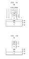
- FIG. 1A is a schematic cross-sectional side view of a portion of a complementary metal oxide semiconductor device at a first-intermediate interconnect fabrication stage, according to an embodiment of the invention.
- FIG. 1B is a schematic cross-sectional side view of a portion of a complementary metal oxide semiconductor device at a second-intermediate interconnect fabrication stage, according to an embodiment of the invention.
- FIG. 1C is a schematic cross-sectional side view of a portion of a complementary metal oxide semiconductor device at a third-intermediate interconnect fabrication stage, according to an embodiment of the invention.
- FIG. 1D is a schematic cross-sectional side view of a portion of a complementary metal oxide semiconductor device at a fourth-intermediate interconnect fabrication stage, according to an embodiment of the invention.
- FIG. 1E is a schematic cross-sectional side view of a portion of a complementary metal oxide semiconductor device at a fifth-intermediate interconnect fabrication stage, according to an embodiment of the invention.
- FIG. 1F is a schematic cross-sectional side view of a portion of a complementary metal oxide semiconductor device at a sixth-intermediate interconnect fabrication stage, according to an embodiment of the invention.
- FIG. 1G is a schematic cross-sectional side view of a portion of a complementary metal oxide semiconductor device at a seventh-intermediate interconnect fabrication stage, according to an embodiment of the invention.
- FIG. 1H is a schematic cross-sectional side view of a portion of a complementary metal oxide semiconductor device at an eighth-intermediate fabrication stage, according to an embodiment of the invention.
- FIG. 1I is a schematic cross-sectional side view of a portion of complementary metal-oxide-semiconductor device at a ninth-intermediate interconnect fabrication stage, according to an embodiment of the invention.
- FIG. 1J is a schematic cross-sectional side view of a portion of a complementary metal oxide semiconductor device at a tenth-intermediate interconnect fabrication stage, according to an embodiment of the invention.
- FIG. 1K is a schematic cross-sectional side view of a portion of a complementary metal oxide semiconductor device at an eleventh-intermediate interconnect fabrication stage, according to an embodiment of the invention.
- illustrative embodiments are provided for metal patterning using a first main-etch process followed by a second over-etch process. More particularly, illustrative embodiments pattern fine copper (Cu) metal lines on an insulating layer of an integrated circuit via a subtractive process (i.e., a process that creates a desired structure by removing material rather than by adding material).
- the subtractive process uses methanol etch chemistry for a main sputter etch process, followed by an over-etch process using selective sputtering with light mass ions.
- the process provides for a well-controlled (e.g., vertically sharpened or about 90 degrees) sidewall profile for metal (Cu) interconnects without tapering.
- a conductive metal layer with sidewalls that form a pyramidal shape is processed so as to result in respective sidewalls that are substantially vertical.
- any improvement in making the sidewalls less pyramidal in shape and more vertical (closer to 90 degrees) is considered beneficial.
- a sidewall angle at or better than about 80-85 degrees is desirable for the tight pitch patterning of Cu for an interconnect application.
- FIGS. 1A-1K are schematic cross-sectional diagrams illustrating various stages of the fabrication of a metal interconnect for a complementary metal oxide semiconductor (CMOS) device 100 , according to embodiments of the present invention. As such, FIGS. 1A-1K also collectively serve as a flow diagram illustrating portions of one or more embodiments of a method for fabricating a portion of CMOS device 100 . It is to be understood that, for the sake of clarity of illustration, while the figures depict fabrication of a single interconnect, the steps of the process of FIGS. 1A-1K are applicable for fabricating multiple such interconnects on CMOS device 100 .
- CMOS complementary metal oxide semiconductor
- CMOS device 100 may also be referred to herein as a CMOS structure or a semiconductor structure, and the CMOS device or structure may be part of an integrated circuit.
- reference numeral 100 is understood to reference a CMOS structure, a CMOS device, and/or a CMOS integrated circuit.
- FIG. 1A illustrates the CMOS device 100 at a first intermediate stage in the processing.
- FIG. 1A illustrates the CMOS device 100 at a first intermediate stage in the processing.
- several fabrication steps leading up to the production of the CMOS device 100 as illustrated in FIG. 1A are omitted.
- the CMOS device 100 does not necessarily start out in the form illustrated in FIG. 1A , but may develop into the illustrated structure over several well-known processing steps which are not illustrated but are well-known to those of ordinary skill in the art.
- the CMOS device 100 comprises a plurality of layers at this intermediate stage in the processing, including: a silicon wafer (silicon substrate) 102 , a first dielectric layer 104 (e.g., comprising silicon dioxide (SiO 2 ), silicon nitride (Si 3 N 4 ), silicon oxynitride (SiON), or a low-k dielectric) formed on the silicon wafer 102 , a first liner layer 106 (e.g., comprising titanium (Ti), titanium nitride (TiN), ruthenium (Ru), tungsten (W), iridium (Ir), gold (Au), platinum (Pt), tantalum (Ta), tantalum nitride (TaN), cobalt (Co), manganese (Mn), manganese oxides (MnO x ), or manganese silicates (MnSi x O y )) formed on the first dielectric layer 104 , a conductive metal layer
- an exemplary range of approximate thickness for each layer comprises: HSQ: 10-50 nm; OPL: 50-300 nm; SiO 2 : 0-150 nm; TaN: 10-200 nm; Ru: 5-30 nm; Cu: 20-100 nm. Thicknesses of other layers (shown and not shown) are determinable by one of ordinary skill in the semiconductor processing art.
- FIG. 1A illustrates the CMOS device 100 at a stage after a small structure has been formed in the organic underlayer 116 and photoresist layer 118 (actually a pattern of small structures is formed but, as mentioned above, only a single one is shown for clarity).
- the organic underlayer 116 and photoresist layer 118 are patterned using a photolithography technique, such as optical lithography or direct write electron beam lithography.
- the photolithography technique includes a negative resist that allows removal of the organic underlayer 116 and photoresist layer 118 down to the second hard mask layer 114 , except for the portions of the organic underlayer 116 and photoresist layer 118 illustrated in FIG. 1A .
- the pattern is transferred from the organic underlayer 116 and photoresist layer 118 to the second hard mask layer 114 .
- pattern transfer involves etching the second hard mask layer 114 down to the first hard mask layer 112 (e.g., using a dry etch process such as reactive ion etching). Pattern transfer results in portions of the second hard mask layer 114 being removed. For instance, in the embodiment illustrated in FIG. 1B , all portions of the second hard mask layer 114 except for the portions residing directly beneath the organic underlayer 116 and photoresist layer 118 are removed down to the first hard mask layer 112 .
- the organic underlayer 116 and photoresist layer 118 are next removed down to the second hard mask layer 114 , leaving the patterned second hard mask layer 114 .
- the pattern is next transferred from the second hard mask layer 114 , which is removed, to the first hard mask layer 112 .
- the pattern transfer from the second hard mask layer 114 to the first hard mask layer 112 is accomplished in a manner similar to that described above (e.g., etching followed by removal of second hard mask material). In the embodiment illustrated in FIG.
- the pattern transfer results in the first hard mask layer 112 being etched down to the protective layer 110 , except for the portion of the first hard mask layer 112 residing directly beneath the second hard mask layer 114 .
- the protective layer 110 protects the Cu material of the conductive metal layer 108 from the RIE chemistry used for the TaN (first hard mask layer 112 ) etch.
- a main plasma etch process is next applied as illustrated in FIG. 1E to remove portions of the protective layer 110 and the conductive metal layer 108 as illustrated in FIG. 1F .
- an argon (Ar) and/or a methanol (CH 3 OH or more generally a C—H—O RIE chemistry) plasma sputter etch process is used to remove the portions of the protective layer 110 and the conductive metal layer 108 .
- C—H—O or C—H or NH 3 (NH 3 or NH 3 —CO or NH 3 -Hydrocarbons) containing plasma can be employed for the main etch process.
- the protective layer 110 is etched except for the portion of the protective layer 110 residing beneath the first hard mask layer 112 , while the conductive metal layer 108 is etched down to the first liner layer 106 , except for the portions of the conductive metal layer 108 substantially residing beneath the first hard mask layer 112 .
- the remaining portions of the conductive metal layer 108 form a metal interconnect (also referred to as a metal line).
- the metal interconnect has a shape in which the base 109 of the metal interconnect is wider than the top 111 of the metal interconnect (for instance, the base may be twice as wide as the top).
- the metal interconnect has a substantially pyramidal profile (having, for example, a sidewall taper of approximately less than 80 degrees, as measured with respect to the horizontal top surface of the first liner layer 106 ).
- the height of the metal interconnect is greater than the width of the metal interconnect at its widest point (e.g., at least 20 percent greater than the width of the base).
- FIGS. 1G and 1H illustrate the second etching process, referred to herein as an over-etch process, comprising selective sputtering with low energy light mass ions, e.g., using helium (He) or dihydrogen (H 2 ) plasma. Alternatively, light mass ion beam process may be employed. More particularly, FIG. 1G illustrates application of the over-etch process to the structure from FIG. 1F , with the results of the over etching depicted in FIG. 1H .
- an over-etch process comprising selective sputtering with low energy light mass ions, e.g., using helium (He) or dihydrogen (H 2 ) plasma.
- light mass ion beam process may be employed. More particularly, FIG. 1G illustrates application of the over-etch process to the structure from FIG. 1F , with the results of the over etching depicted in FIG. 1H .
- Light mass ions such as He or H 2
- This selective sputtering provides a distinct advantage in controlling the conductive metal layer profile, in this example, the Cu profile, resulting in substantially vertical sidewalls for the conductive metal (Cu) feature.
- the low energy light mass ion plasma over-etch achieves a nearly 90 degree sidewall taper angle of the conductive metal layer 108 , while not effecting the first liner layer 106 or the first hard mask layer 112 and the protective layer 110 .
- He plasma in accordance with an illustrative embodiment having an ion energy less than approximately 500 electron volts (eV), is very selective to the first hard mask layer 112 and the bottom liner (layer 106 ) comprising Ta/TaN. While the main etch has a high etch rate typically greater than approximately 1 nanometer per second (nm/s) wherein the exposure time may be on the order of approximately 10-30 seconds, an exposure time of approximately 1-10 minutes to the He plasma at an etch rate of approximately 5-10 nm/min (nanometers/minute) results in achieving the vertical (sharpened) sidewalls.
- the resulting structure advantageously allows for a tighter pitch of the Cu conductor, e.g., smaller than approximately 100 nm pitch.
- FIGS. 1I though 1 K illustrate remaining steps in fabricating the metal interconnect in the CMOS device 100 .
- a liner 120 is formed over the CMOS device 100 coating portions of the first liner layer 106 , the vertical sidewalls of the conductive metal layer 108 and the protective layer 110 , and the first hard mask layer 112 .
- the liner 120 is deposited by atomic layer deposition or related techniques (e.g., physical vapor deposition).
- a mask layer 122 is then deposited over liner 120 .
- liner 120 may comprise about 0.5-5 nm Ta, Co, or Ru, while mask layer 122 may comprise about 0.5-5 nm TaN, TiN, Mn, or MnO.
- the portion of the liner layer 120 that coats the first liner layer 106 and the corresponding portion of the mask layer 122 , the first liner layer 106 under the liner layer 120 , and all of the first hard mask layer 112 , are removed.
- the portions of the liner 120 coating the sidewalls of the conductive metal layer 108 and the protective layer 110 , and the corresponding portion of the mask layer 122 remain intact.
- a dielectric layer 124 (e.g., comprising a low-k dielectric material for which k is less than approximately 4.0) is next deposited over the CMOS device 100 and planarized (e.g., chemical-mechanical planarization). Any suitable interconnect dielectrics can be applied, e.g., SiO, SiCO, SiN, SiNC, or SiCON, coated by chemical vapor deposition (CVD) or spun on. Specifically, the dielectric layer 124 fills in the empty space in the CMOS device 100 , coating portions of the first dielectric layer 104 , the liner layer 106 , the liner 120 , the mask layer 122 , and the protective layer 110 .
- CVD chemical vapor deposition
- the resultant structure thus includes a trench (i.e., the interior volumes defined by the dielectric 104 , the first liner layer 106 , the liner 120 , and the mask layer 122 , which collectively form a conformal liner for the trench) containing a fine metal interconnect or line (i.e., the conductive metal layer 108 ).
- a trench i.e., the interior volumes defined by the dielectric 104 , the first liner layer 106 , the liner 120 , and the mask layer 122 , which collectively form a conformal liner for the trench
- a fine metal interconnect or line i.e., the conductive metal layer 108 .
- integrated circuit dies can be fabricated with various devices such as transistors, diodes, capacitors, inductors, etc.
- An integrated circuit in accordance with embodiments can be employed in applications, hardware, and/or electronic systems. Suitable hardware and systems for implementing the invention may include, but are not limited to, personal computers, communication networks, electronic commerce systems, portable communications devices (e.g., cell phones), solid-state media storage devices, functional circuitry, etc. Systems and hardware incorporating such integrated circuits are considered part of the embodiments described herein.
- various layers, regions, and/or structures described above may be implemented in integrated circuits (chips).
- the resulting integrated circuit chips can be distributed by the fabricator in raw wafer form (that is, as a single wafer that has multiple unpackaged chips), as a bare die, or in a packaged form.
- the chip is mounted in a single chip package (such as a plastic carrier, with leads that are affixed to a motherboard or other higher level carrier) or in a multichip package (such as a ceramic carrier that has either or both surface interconnections or buried interconnections).
- the chip is then integrated with other chips, discrete circuit elements, and/or other signal processing devices as part of either (a) an intermediate product, such as a motherboard, or (b) an end product.
- the end product can be any product that includes integrated circuit chips, ranging from toys and other low-end applications to advanced computer products having a display, a keyboard or other input device, and a central processor.
Landscapes
- Engineering & Computer Science (AREA)
- Physics & Mathematics (AREA)
- Power Engineering (AREA)
- General Physics & Mathematics (AREA)
- Computer Hardware Design (AREA)
- Microelectronics & Electronic Packaging (AREA)
- Condensed Matter Physics & Semiconductors (AREA)
- Manufacturing & Machinery (AREA)
- High Energy & Nuclear Physics (AREA)
- Plasma & Fusion (AREA)
- Geometry (AREA)
- Health & Medical Sciences (AREA)
- Toxicology (AREA)
- Internal Circuitry In Semiconductor Integrated Circuit Devices (AREA)
Abstract
Description
Claims (18)
Priority Applications (1)
| Application Number | Priority Date | Filing Date | Title |
|---|---|---|---|
| US15/192,196 US9799519B1 (en) | 2016-06-24 | 2016-06-24 | Selective sputtering with light mass ions to sharpen sidewall of subtractively patterned conductive metal layer |
Applications Claiming Priority (1)
| Application Number | Priority Date | Filing Date | Title |
|---|---|---|---|
| US15/192,196 US9799519B1 (en) | 2016-06-24 | 2016-06-24 | Selective sputtering with light mass ions to sharpen sidewall of subtractively patterned conductive metal layer |
Publications (1)
| Publication Number | Publication Date |
|---|---|
| US9799519B1 true US9799519B1 (en) | 2017-10-24 |
Family
ID=60082885
Family Applications (1)
| Application Number | Title | Priority Date | Filing Date |
|---|---|---|---|
| US15/192,196 Expired - Fee Related US9799519B1 (en) | 2016-06-24 | 2016-06-24 | Selective sputtering with light mass ions to sharpen sidewall of subtractively patterned conductive metal layer |
Country Status (1)
| Country | Link |
|---|---|
| US (1) | US9799519B1 (en) |
Cited By (8)
| Publication number | Priority date | Publication date | Assignee | Title |
|---|---|---|---|---|
| US10373747B2 (en) * | 2017-01-11 | 2019-08-06 | International Business Machines Corporation | Magnetic inductor stacks |
| US10593449B2 (en) | 2017-03-30 | 2020-03-17 | International Business Machines Corporation | Magnetic inductor with multiple magnetic layer thicknesses |
| US10597769B2 (en) | 2017-04-05 | 2020-03-24 | International Business Machines Corporation | Method of fabricating a magnetic stack arrangement of a laminated magnetic inductor |
| US10607759B2 (en) | 2017-03-31 | 2020-03-31 | International Business Machines Corporation | Method of fabricating a laminated stack of magnetic inductor |
| CN112053951A (en) * | 2019-06-06 | 2020-12-08 | 美光科技公司 | Method for integrated circuit fabrication |
| US11170933B2 (en) | 2017-05-19 | 2021-11-09 | International Business Machines Corporation | Stress management scheme for fabricating thick magnetic films of an inductor yoke arrangement |
| US11276732B2 (en) | 2019-09-20 | 2022-03-15 | International Business Machines Corporation | Semiconductor memory devices formed using selective barrier metal removal |
| TWI797525B (en) * | 2019-12-27 | 2023-04-01 | 日商日立全球先端科技股份有限公司 | Manufacturing method of semiconductor device |
Citations (6)
| Publication number | Priority date | Publication date | Assignee | Title |
|---|---|---|---|---|
| US8633117B1 (en) | 2012-11-07 | 2014-01-21 | International Business Machines Corporation | Sputter and surface modification etch processing for metal patterning in integrated circuits |
| US20140162448A1 (en) * | 2010-07-30 | 2014-06-12 | SK Hynix Inc. | Semiconductor device with metal gates and method for fabricating the same |
| US8871107B2 (en) | 2013-03-15 | 2014-10-28 | International Business Machines Corporation | Subtractive plasma etching of a blanket layer of metal or metal alloy |
| US20150014152A1 (en) | 2013-07-12 | 2015-01-15 | International Business Machines Corporation | Selective sputtering for pattern transfer |
| US9171796B1 (en) | 2014-06-19 | 2015-10-27 | International Business Machines Corporation | Sidewall image transfer for heavy metal patterning in integrated circuits |
| US9257638B2 (en) * | 2014-03-27 | 2016-02-09 | Lam Research Corporation | Method to etch non-volatile metal materials |
-
2016
- 2016-06-24 US US15/192,196 patent/US9799519B1/en not_active Expired - Fee Related
Patent Citations (9)
| Publication number | Priority date | Publication date | Assignee | Title |
|---|---|---|---|---|
| US20140162448A1 (en) * | 2010-07-30 | 2014-06-12 | SK Hynix Inc. | Semiconductor device with metal gates and method for fabricating the same |
| US8633117B1 (en) | 2012-11-07 | 2014-01-21 | International Business Machines Corporation | Sputter and surface modification etch processing for metal patterning in integrated circuits |
| US9064727B2 (en) | 2012-11-07 | 2015-06-23 | International Business Machines Corporation | Sputter and surface modification etch processing for metal patterning in integrated circuits |
| US20150243602A1 (en) | 2012-11-07 | 2015-08-27 | International Business Machines Corporation | Sputter and surface modification etch processing for metal patterning in integrated circuits |
| US9263393B2 (en) | 2012-11-07 | 2016-02-16 | Globalfoundries Inc. | Sputter and surface modification etch processing for metal patterning in integrated circuits |
| US8871107B2 (en) | 2013-03-15 | 2014-10-28 | International Business Machines Corporation | Subtractive plasma etching of a blanket layer of metal or metal alloy |
| US20150014152A1 (en) | 2013-07-12 | 2015-01-15 | International Business Machines Corporation | Selective sputtering for pattern transfer |
| US9257638B2 (en) * | 2014-03-27 | 2016-02-09 | Lam Research Corporation | Method to etch non-volatile metal materials |
| US9171796B1 (en) | 2014-06-19 | 2015-10-27 | International Business Machines Corporation | Sidewall image transfer for heavy metal patterning in integrated circuits |
Non-Patent Citations (3)
| Title |
|---|
| IBM.com, "Copper Interconnects: The Evolution of Microprocessors," http://www-03.ibm.com/ibm/history/ibm100/us/en/icons/copperchip/, Apr. 11, 2015, 3 pages. |
| Wikipedia, "Copper Interconnect," https://en.wikipedia.org/wiki/Copper-interconnect, Jan. 14, 2016, 3 pages. |
| Wikipedia, "Copper Interconnect," https://en.wikipedia.org/wiki/Copper—interconnect, Jan. 14, 2016, 3 pages. |
Cited By (17)
| Publication number | Priority date | Publication date | Assignee | Title |
|---|---|---|---|---|
| US10373747B2 (en) * | 2017-01-11 | 2019-08-06 | International Business Machines Corporation | Magnetic inductor stacks |
| US10593449B2 (en) | 2017-03-30 | 2020-03-17 | International Business Machines Corporation | Magnetic inductor with multiple magnetic layer thicknesses |
| US10593450B2 (en) | 2017-03-30 | 2020-03-17 | International Business Machines Corporation | Magnetic inductor with multiple magnetic layer thicknesses |
| US11361889B2 (en) | 2017-03-30 | 2022-06-14 | International Business Machines Corporation | Magnetic inductor with multiple magnetic layer thicknesses |
| US10607759B2 (en) | 2017-03-31 | 2020-03-31 | International Business Machines Corporation | Method of fabricating a laminated stack of magnetic inductor |
| US11222742B2 (en) | 2017-03-31 | 2022-01-11 | International Business Machines Corporation | Magnetic inductor with shape anisotrophy |
| US10597769B2 (en) | 2017-04-05 | 2020-03-24 | International Business Machines Corporation | Method of fabricating a magnetic stack arrangement of a laminated magnetic inductor |
| US11479845B2 (en) | 2017-04-05 | 2022-10-25 | International Business Machines Corporation | Laminated magnetic inductor stack with high frequency peak quality factor |
| US11170933B2 (en) | 2017-05-19 | 2021-11-09 | International Business Machines Corporation | Stress management scheme for fabricating thick magnetic films of an inductor yoke arrangement |
| US11367569B2 (en) | 2017-05-19 | 2022-06-21 | International Business Machines Corporation | Stress management for thick magnetic film inductors |
| US10971500B2 (en) * | 2019-06-06 | 2021-04-06 | Micron Technology, Inc. | Methods used in the fabrication of integrated circuitry |
| US20200388622A1 (en) * | 2019-06-06 | 2020-12-10 | Micron Technology, Inc. | Methods Used In The Fabrication Of Integrated Circuitry |
| CN112053951A (en) * | 2019-06-06 | 2020-12-08 | 美光科技公司 | Method for integrated circuit fabrication |
| CN112053951B (en) * | 2019-06-06 | 2024-10-18 | 美光科技公司 | Method for integrated circuit fabrication |
| US11276732B2 (en) | 2019-09-20 | 2022-03-15 | International Business Machines Corporation | Semiconductor memory devices formed using selective barrier metal removal |
| US11647639B2 (en) | 2019-09-20 | 2023-05-09 | International Business Machines Corporation | Conductive bridging random access memory formed using selective barrier metal removal |
| TWI797525B (en) * | 2019-12-27 | 2023-04-01 | 日商日立全球先端科技股份有限公司 | Manufacturing method of semiconductor device |
Similar Documents
| Publication | Publication Date | Title |
|---|---|---|
| US9799519B1 (en) | Selective sputtering with light mass ions to sharpen sidewall of subtractively patterned conductive metal layer | |
| US12159838B2 (en) | Method of forming an interconnect structure having an air gap and structure thereof | |
| US9754882B2 (en) | Interconnect structure having air gap and method of forming the same | |
| CN107230660B (en) | Manufacturing method of semiconductor device | |
| US10867921B2 (en) | Semiconductor structure with tapered conductor | |
| US20190096757A1 (en) | Thin film interconnects with large grains | |
| US10586733B2 (en) | Multi-level air gap formation in dual-damascene structure | |
| US8871107B2 (en) | Subtractive plasma etching of a blanket layer of metal or metal alloy | |
| US9263393B2 (en) | Sputter and surface modification etch processing for metal patterning in integrated circuits | |
| US10157833B1 (en) | Via and skip via structures | |
| US8980745B1 (en) | Interconnect structures and methods of forming same | |
| US8168528B2 (en) | Restoration method using metal for better CD controllability and Cu filing | |
| US9911648B2 (en) | Interconnects based on subtractive etching of silver | |
| US9385086B2 (en) | Bi-layer hard mask for robust metallization profile | |
| US6541863B1 (en) | Semiconductor device having a reduced signal processing time and a method of fabricating the same | |
| US9484220B2 (en) | Sputter etch processing for heavy metal patterning in integrated circuits | |
| US20140124935A1 (en) | Sputter and surface modification etch processing for metal patterning in integrated circuits | |
| JP2009164175A (en) | Method for fabricating semiconductor device | |
| US20230197511A1 (en) | Double patterning with selectively deposited spacer | |
| US20240387254A1 (en) | Semiconductor structure and method for forming the same |
Legal Events
| Date | Code | Title | Description |
|---|---|---|---|
| AS | Assignment |
Owner name: INTERNATIONAL BUSINESS MACHINES CORPORATION, NEW Y Free format text: ASSIGNMENT OF ASSIGNORS INTEREST;ASSIGNORS:JOSEPH, ERIC A.;MIYAZOE, HIROYUKI;REEL/FRAME:039155/0787 Effective date: 20160623 |
|
| STCF | Information on status: patent grant |
Free format text: PATENTED CASE |
|
| AS | Assignment |
Owner name: ELPIS TECHNOLOGIES INC., CANADA Free format text: ASSIGNMENT OF ASSIGNORS INTEREST;ASSIGNOR:INTERNATIONAL BUSINESS MACHINES CORPORATION;REEL/FRAME:052644/0868 Effective date: 20200306 |
|
| FEPP | Fee payment procedure |
Free format text: MAINTENANCE FEE REMINDER MAILED (ORIGINAL EVENT CODE: REM.); ENTITY STATUS OF PATENT OWNER: LARGE ENTITY |
|
| LAPS | Lapse for failure to pay maintenance fees |
Free format text: PATENT EXPIRED FOR FAILURE TO PAY MAINTENANCE FEES (ORIGINAL EVENT CODE: EXP.); ENTITY STATUS OF PATENT OWNER: LARGE ENTITY |
|
| STCH | Information on status: patent discontinuation |
Free format text: PATENT EXPIRED DUE TO NONPAYMENT OF MAINTENANCE FEES UNDER 37 CFR 1.362 |
|
| FP | Lapsed due to failure to pay maintenance fee |
Effective date: 20211024 |