US9798852B2 - Methods of design rule checking of circuit designs - Google Patents
Methods of design rule checking of circuit designs Download PDFInfo
- Publication number
- US9798852B2 US9798852B2 US15/040,235 US201615040235A US9798852B2 US 9798852 B2 US9798852 B2 US 9798852B2 US 201615040235 A US201615040235 A US 201615040235A US 9798852 B2 US9798852 B2 US 9798852B2
- Authority
- US
- United States
- Prior art keywords
- design
- verification
- line
- lines
- line end
- Prior art date
- Legal status (The legal status is an assumption and is not a legal conclusion. Google has not performed a legal analysis and makes no representation as to the accuracy of the status listed.)
- Expired - Fee Related, expires
Links
Images


Classifications
-
- G06F17/5081—
-
- G—PHYSICS
- G06—COMPUTING OR CALCULATING; COUNTING
- G06F—ELECTRIC DIGITAL DATA PROCESSING
- G06F30/00—Computer-aided design [CAD]
- G06F30/30—Circuit design
- G06F30/39—Circuit design at the physical level
- G06F30/398—Design verification or optimisation, e.g. using design rule check [DRC], layout versus schematics [LVS] or finite element methods [FEM]
-
- H—ELECTRICITY
- H01—ELECTRIC ELEMENTS
- H01L—SEMICONDUCTOR DEVICES NOT COVERED BY CLASS H10
- H01L21/00—Processes or apparatus adapted for the manufacture or treatment of semiconductor or solid state devices or of parts thereof
- H01L21/02—Manufacture or treatment of semiconductor devices or of parts thereof
- H01L21/027—Making masks on semiconductor bodies for further photolithographic processing not provided for in group H01L21/18 or H01L21/34
-
- H10P76/00—
-
- G—PHYSICS
- G06—COMPUTING OR CALCULATING; COUNTING
- G06F—ELECTRIC DIGITAL DATA PROCESSING
- G06F2119/00—Details relating to the type or aim of the analysis or the optimisation
- G06F2119/18—Manufacturability analysis or optimisation for manufacturability
-
- G06F2217/12—
Definitions
- the present invention relates to performing design rule checking of a circuit design, and more particularly, performing design rule checking with a design rule checking tool according to a verification pattern.
- SADP self-aligned double-patterning
- unidirectional lines are first formed, for example, by use of spacer process and a subsequent block mask step, using a block mask pattern, may be applied to form the line ends.
- SADP process may be implemented to manufacture a metal route layout. The route layout for metal line formation is often generated by automation tools following a set of predefined metal design rules.
- an EDA route tool often forms only metal line patterns and does not perform the block mask step. Consequently, the route layout may not successfully pass a block mask design rule check. Therefore, there is a need to develop a method of metal line design rule check that can ensure passing block mask design rule check.
- a method including: providing a circuit design for an integrated circuit layer, the circuit design including a plurality of design lines oriented in a same defined direction; automatically performing a design rule check of the circuit design by a design rule checking tool, in which the automatically performing includes: forming, by the design rule checking tool, a verification pattern for the circuit design, the verification pattern having a plurality of verification lines and a plurality of verification regions, the verification lines being defined, in part, by one or more adjacent design line ends, and wherein one or more verification regions of the plurality of verification regions are defined, in part, by one or more critical dimensions of the circuit design and are associated with and connected to one verification line of the plurality of verification lines; and, checking, by the design rule checking tool, the verification pattern for any verification line overlapping a verification region.
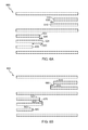
- FIG. 1 depicts one embodiment of a circuit design overlaid with a portion of a blocking mask, illustrating some of the issues associated with various circuit layer fabrication techniques
- FIGS. 2A-2B depict embodiments of portions of circuit designs undergoing design rule checking
- FIGS. 3A-3D depict embodiments of similar circuit designs undergoing design rule checking, illustrating certain problems and limitations of design rule checking processes
- FIGS. 4A-4F depict one embodiment of a process for automatically performing design rule checking, in which a verification pattern is formed that overcomes the problems and limitations illustrated by FIGS. 3A-3D , in accordance with one or more aspects of the present invention
- FIGS. 5A-5B depict the circuit designs of FIGS. 3A-3D undergoing one embodiment of a process for automatically performing design rule checking as depicted by FIGS. 4A-4F , in accordance with one or more aspects of the present invention.
- FIGS. 6A-6C depict one alternative embodiment of a process for automatically performing design rule checking, in accordance with one or more aspects of the present invention.
- a method including: providing a circuit design for an integrated circuit layer, the circuit design including a plurality of design lines oriented in a defined direction; automatically performing a design rule check of the circuit design by a design rule checking tool, in which the performing includes: forming a verification pattern for the circuit design, the verification pattern having a plurality of verification lines and a plurality of verification regions, the verification lines being defined, in part, by one or more adjacent design line ends, and wherein one or more verification regions of the plurality of verification regions are defined, in part, by one or more critical dimensions of the circuit design and are associated with and connected to one verification line of the plurality of verification lines; and, checking the verification pattern for any verification line overlapping a verification region.
- FIG. 1 depicts one embodiment of a circuit design 100 overlaid by a portion of a block mask pattern 120 .
- Circuit design 100 may include a plurality of design lines 110 oriented in a defined direction.
- Design lines 110 may have varying lengths and may, as illustrated in FIG. 1 , have a uniform line width.
- Design lines 110 of circuit design 100 may correspond, for example, to metallization lines of a circuit structure, raised fin structures, gate structures, or other features of an integrated circuit layer.
- Fabricating an integrated circuit layer according to circuit design 100 may include, for example, a self-aligned double-patterning process (SADP).
- SADP self-aligned double-patterning process
- Routing tools may frequently be used for patterning processes such as SADP due to their ability to rapidly pattern linear circuit layer features, such as a pattern of metal lines corresponding to design lines 110 .
- a decomposition tool may subsequently be used to generate a block mask pattern and continue patterning of the circuit structure.
- Design lines patterned by a routing tool generally need to be formed so that a corresponding block mask pattern generated by the decomposition tool will pass a design rule check.
- routing tools are generally configured only to generate design lines and not block mask patterns, in order to preserve the efficiency and speed of the routing tool, routing tools may only be configured to perform a design rule check according to design lines 110 which may not ensure that a corresponding block mask pattern will pass a design rule check.
- block masks of a block mask pattern generally must be separated from each other by a defined minimum separation, for example, the separation 125 between block masks 121 and 122 of block mask pattern 120 must be equal to or greater than a defined minimum separation for block mask pattern 120 .
- This minimum separation of block masks may be necessary, in part, because of light diffraction at or near the edges of individual block masks.
- block masks 121 and 122 generally must have minimum length dimensions, such as a minimum height and minimum width, to facilitate minimizing diffraction effects. Such defects in resulting metal lines may short a circuit or allow electrical connections between circuit features that must be electrically isolated.
- an automated design rule check (DRC) process may be applied to either or both the circuit design and block mask pattern, prior to actual fabrication of the circuit layer, to ensure that the routing tool will accurately reproduce the intended circuit design on the fabricated circuit layer without significant defects.
- DRC design rule check
- FIGS. 2A and 2B depict example embodiments of how a design rule check process may be applied to circuit designs in order to ensure that the circuit design and/or block mask pattern meet one or more design rules, such as a minimum separation of block masks or minimum length dimensions of block masks.
- Design rule checks may involve, for example, identifying individual ends of design lines in a circuit design, and forming one or more “keep-out” regions associated with each end of a design line.
- the “keep-out” regions sometimes also called “forbidden regions,” are so named because design line ends must be kept out of the “keep-out” regions.
- Keep-out regions may be rectangular regions, and may have height and width dimensions defined by one or more critical dimensions of the circuit design and/or a block mask pattern intended for use with the circuit design.
- a design rule check process may look for any design line end falling within a keep-out region associated with another design line end. If a design line end is found within a keep-out region, the circuit design (or at least that portion of the circuit design) fails the design rule check. In general, if no end of a design line falls within the keep-out regions of any other design lines, then a corresponding block mask pattern should have large enough block masks separated by at least a defined minimum separation, and the circuit design thus may pass the design rule check.
- FIG. 2A depicts a portion of an embodiment of a circuit design 200 having a plurality of design lines 210 , 215 , and 220 .
- keep-out region 230 associated with an end of design line 220 is shown; in practice, the end of any one design line may have multiple keep-out regions associated with it.
- keep-out region 230 is connected to design line 220 and centered on the end of design line 220 .
- FIG. 2A illustrates, no end of any other design line 210 , 215 falls within the keep-out region 230 for the end of design line 220 , as desired.
- a portion of design line 215 does fall within keep-out region 230 , but because this portion is not an end of design line 215 the design does not fail the design rule check.
- FIG. 2B depicts a portion of an embodiment of another circuit design 250 having a plurality of design lines 260 , 270 , 280 .
- One example keep-out region 290 associated with an end of design line 270 is depicted; here, keep-out region 290 is connected to a side of design line 270 , with the connecting side of keep-out region 290 centered at the end of design line 270 .
- an end 285 of design line 280 falls within keep-out region 290 of design line 270 .
- circuit design 250 would fail the design rule check; in practice, if this circuit design and a corresponding block mask pattern were used, the resulting circuit layer would likely have one or more defectively formed lines due to the close proximity of the block masks in the block mask pattern.
- FIGS. 3A-3D illustrate some of these limitations.
- FIG. 3A depicts an embodiment of a circuit design 300 that may be generated by a SADP route tool and an associated block mask pattern 320 that may be used with circuit design 300 to form a circuit layer. It is may be noted that block mask pattern 320 is generated after metal line design routing by a decomposition process and is not visible in the routing process. As FIG.
- circuit design 300 includes a plurality of design lines 310 , with one uninterrupted design line 313 in the middle.
- a block mask pattern 320 may be generated by an additional decomposition process.
- block mask pattern may include block masks 321 and 322 , the block masks 321 and 322 separated by a span 325 to allow design line 313 to remain uninterrupted.
- separation 325 between block masks 321 , 323 may be less than a defined minimum separation 330 for block mask pattern 320 .
- a defined minimum separation for a block mask pattern may require that any two block masks of the block mask pattern be separated by at least two design lines 310 or two metal lines. Block masks separated by less than this distance may be formed too close together and may result in defectively formed lines, as described above.
- FIG. 3B depicts a circuit design 350 similar to circuit design 300 of FIG. 3A , but without the central uninterrupted design line 313 of circuit design 300 . Instead, circuit design 350 has separated central design lines 363 and 364 , similar to other adjacent design lines 360 of circuit design 350 .
- a block mask pattern 370 corresponding to circuit design 350 may include one block mask 371 , instead of two separate block masks. As noted above for FIG. 3A , block mask pattern 370 may be generated after routing by a separate decomposition process and not be visible to or checked by the route tool. Because block mask 371 is not close to another block mask, unlike block masks 321 and 322 in FIG. 3A , block mask pattern 370 may not violate any design rules for circuit design 350 . Unlike circuit design 300 , which should fail a design rule check, circuit design 350 should pass a design rule check.
- FIGS. 3C and 3D illustrate circuit designs 300 and 350 , respectively, undergoing the same design rule check process in the process of metal design line routing.
- no block mask pattern will be generated by the route tool and no block mask design rule check will be done in the routing process. Therefore, metal line design rule check must be designed to ensure that block mask pattern can be successfully manufactured, which, however, is not practical in some specific designs.
- design line ends 311 and 312 may be examined by a metal line design rule check process. Examples of keep-out regions 331 and 332 , associated with design line ends 311 and 312 respectively, are depicted in FIG. 3C ; other possible keep-out regions are not depicted here for simplicity. As FIG.
- circuit design 300 should fail a design rule check.
- the portion of design line 313 falling within keep-out regions 331 and 332 does not, by itself, cause the circuit design 300 to fail the design rule check because those portions of design line 313 are not ends of design line 313 .
- the presence of design line 313 would require the placement of block masks 321 and 322 , as depicted in FIG. 3A , in block mask pattern 320 for proper formation of a circuit layer according to circuit design 300 .
- FIG. 3D depicts circuit design 350 undergoing the same design rule check process as circuit design 300 .
- design lines 361 and 362 correspond to design lines 311 and 312 , respectively, in FIG. 3A .
- keep-out regions 381 and 382 are associated with design lines 361 and 362 , similar to keep-out regions 321 and 322 in FIG. 3A .
- Applying the same design rule check process to circuit design 350 also results in the circuit design 350 failing the design rule check because ends of some design lines 310 fall within keep-out regions 381 and 382 .
- circuit design 350 should pass the design rule check because the required block mask pattern 370 would not violate any design rules.
- circuit design 300 and 350 were part of a larger circuit design for an integrated circuit layer, the design rule check process might incorrectly identify portions of the circuit design that need to be corrected, such as the portion depicted by circuit design 350 . However, if the parameters of the design rule check were adjusted in order to correctly identify circuit design 350 as passing the design rule check, the same design rule check would likely identify circuit design 300 as passing the design rule check as well. While multiple iterations of the design rule checking process could be carried out to properly check both circuit designs 300 and 350 , the time and costs involved in carrying out multiple iterations may be prohibitively high. Therefore, there is a need for metal design rule check that can successfully fail the design as shown in FIG. 3C while passing the design as shown in FIG. 3D .
- FIGS. 4A-4F depict one embodiment of a process for performing a design rule check that may address issues with design rule check processes as described herein.
- Performing the design rule check may be done automatically, for example by a design rule checking tool.
- performing the design rule check may include forming a verification pattern for the circuit design, as further described below.
- the verification pattern may include a plurality of verification lines and a plurality of verification regions.
- the verification lines may be defined, in part, by one or more adjacent design line ends.
- One or more verification regions of the plurality of verification regions may be defined, in part, by one or more critical dimensions of the circuit design, and may be associated with and connected to one verification line of the plurality of verification lines.
- the verification regions of the verification pattern may be similar to “keep-out regions” as described above.
- the design rule check may further include checking the verification pattern for any verification line that overlaps a verification region, which may be a verification region associated with another verification line of the verification pattern.
- FIG. 4A depicts an embodiment of a circuit design 400 including a plurality of design lines that may be provided and that may undergo a design rule check, using a verification pattern formed as described further below, prior to being used for fabrication of an integrated circuit layer.
- Forming of the verification pattern may include, for example, identifying one or more adjacent design lines having adjacent design line ends. Identifying the one or more adjacent design lines having the one or more adjacent design line ends may include identifying, for example, a first design line and a second design line that are adjacent in a direction transverse to the defined direction of the design lines of circuit design 400 .
- a separation, in the defined direction of the design lines, between first design line end and second design line end may be determined, and the first design line end and second design line end may be defined to be adjacent design line ends if the separation is determined to be equal to or less than a defined minimum separation. If the first design line end and second design line end have a separation greater than the defined minimum separation, then the first and second design line ends are defined to not be adjacent line ends (see FIGS. 6A-6C ).
- first and second design line ends 411 , 412 may be identified 410 as being vertically adjacent to each other.
- a separation in the horizontal direction (i.e., the defined direction of the design lines) between first design line end 411 and second design line end 412 may be determined, and the separation compared to a defined minimum separation.
- first and second design line ends 411 , 412 have a separation of zero in the defined direction (e.g., horizontal) of the design lines, thus first and second design line ends 411 , 412 may be identified as being adjacent design line ends for the purposes of forming a verification pattern.
- first design line end 411 and second design line end 412 in a direction transverse to the defined direction may not define whether first design line end 411 and second design line end 412 are adjacent design line ends, however such a transverse separation may facilitate identifying design lines that are adjacent in the direction transverse to the defined direction.
- first design line end 421 and second design line end 422 may also be identified 420 as being adjacent design line ends within circuit design 400 .
- the process of forming a verification line may further include identifying a third design line 423 adjacent to second design line 422 and determining a separation, in the defined direction, between second design line end 422 and third design line end 423 . If the separation is less than the defined minimum separation, then first design line end 421 , second design line end 422 , and third design line end 423 together may be defined to be adjacent line ends.
- a group of adjacent design line ends may have any number of adjacent design line ends.
- the defined minimum separation in the defined direction of the design lines, may be defined, in one example, to be zero. That is, for a define minimum separation of zero, two design line ends are defined to be adjacent only when the design line ends are aligned so that a verification line spanning the design line ends is a straight line.
- the defined minimum separation may be defined by a critical dimension of a block mask pattern having a plurality of masking blocks, where the block mask pattern is designed to be used to form the integrated circuit layer according to the circuit design.
- a critical dimension of the block mask pattern may be a minimum length dimension of a masking block of the plurality of masking blocks, such as a minimum height or minimum width of a masking block.
- block mask patterns may be formed on a reticle and may include a plurality of masking blocks.
- the masking blocks may be regular or irregular polygons, as determined in part by a corresponding circuit design, and may have one or more minimum length dimensions, such as a minimum height dimension or minimum width dimension.
- Minimum length dimensions of masking blocks may be defined, in part, by a wavelength of light used by a lithography tool, as masking blocks having sizes much smaller than this wavelength may undesirably increase diffraction and interference effects, potentially resulting in a greater number of defects on the fabricated circuit layer.
- Minimum length dimensions of masking blocks may also be defined by a minimum block size that can be accurately formed on the reticle.
- FIG. 4B depicts one embodiment of forming one verification line 450 of a plurality of verification lines for a verification pattern that may be used to perform design rule checking of circuit design 400 .
- first design line end 411 and second design line end 412 may be identified as being the one or more adjacent design line ends.
- Verification line 450 may be formed to span the one or more adjacent line ends 411 and 412 , and thus may span first design line end 411 , second design line end 412 , and a space between first and second design line ends 411 , 412 , as shown.
- Forming verification line 450 may be considered “grouping” first and second design line ends 411 and 412 for design rule check purposes.
- Verification line 450 is not formed as part of circuit design 400 and does not alter circuit design 400 ; verification line 450 , and associated verification regions formed as described in the examples below, is part of a separate verification pattern formed for the design rule checking processes described herein. In one example, a verification line may include only a single design line end.
- FIG. 4C depicts one embodiment of forming one or more verification regions 451 , 452 that are associated with and connected to the one verification line 450 of a plurality of verification lines of the verification pattern.
- Verification region 451 may be rectangular region having one or both of a height 451 a and width 451 b defined by one or more critical dimensions of the circuit design 400 .
- a critical dimension of circuit design 400 may, for example, be a minimum separation, in the defined direction, between two co-linear design lines of the plurality of design lines.
- one or both of the height and width of the rectangular region may be defined by one or more critical dimensions of a block mask pattern including a plurality of masking blocks, such as a block mask pattern as previously described herein.
- one critical dimension of a block mask pattern may be a minimum length dimension of a masking block of the plurality of masking blocks.
- a critical dimension of a block mask pattern may be a defined minimum separation between two or more masking blocks of the block mask pattern.
- Verification region 451 may be associated with and connected to verification line 450 at one end of verification line 450 .
- a side of verification region 451 connected to verification line 450 may be centered with respect to verification line 450 , for example as depicted in FIG. 4C .
- Verification region 452 which may be a rectangular region similar to verification region 451 , may be associated with and connected to verification line 450 at another end of verification line 450 .
- a side of verification region 452 connected to verification line 450 may be centered with respect to verification line 450 , as in the example embodiment depicted in FIG. 4C .
- FIG. 4D depicts another embodiment of forming one or more verification regions 453 that are associated with and connected to the one verification line 450 of a plurality of verification lines of the verification pattern.
- Verification region 453 may be rectangular region having one or both of a height 453 a and width 453 b defined by one or more critical dimensions of the circuit design 400 , such as a separation, in the defined direction of the design lines, between two co-linear design lines of the plurality of design lines.
- one or both of the height and width of the rectangular region may be defined by one or more critical dimensions of a block mask pattern including a plurality of masking blocks, such as a defined minimum separation between two or more masking blocks or a minimum length dimension of a masking block the block mask pattern.
- Verification region 453 may be associated and connected to verification line 450 at, for example, a central portion of verification line 450 .
- a side of verification region 453 connected to verification line 450 may be centered with respect to verification line 450 , for example as depicted in FIG. 4D .
- FIG. 4E depicts an embodiment of forming one or more verification regions of a verification pattern including each of verification regions 451 , 452 , and 453 as described above.
- a verification line such as verification line 450 may have multiple verification regions associated with and connected to the verification line 450 .
- Verification regions 451 , 452 , and 453 may overlap, as FIG. 4E depicts, or may not overlap at all, depending in part on the span of verification line 450 and the dimensions of the verification regions, as defined by the one or more critical dimensions of circuit design 400 .
- FIG. 4F depicts the circuit design 400 of FIGS. 4B-4E with another verification line 460 spanning adjacent design line ends 421 , 422 , and 423 , and one or more verification regions 465 associated with and connected to verification line 460 .
- the one or more verification regions 455 associated with verification line 450 and the one or more verification regions 465 associated with verification line 460 are depicted in FIG. 4F as single, contiguous verification regions 455 and 465 rather than as multiple overlapping verification regions for each verification line.
- the process of forming the verification pattern as described herein may include, in alternative embodiments, concatenating one or more verification regions associated with a verification line into a single verification region associated with the verification line.
- FIG. 4F also depicts, in part, checking the verification pattern for any verification line overlapping a verification region, as part of automatically performing a design rule check of the circuit design.
- the design rule checking tool may check verification region 455 for any verification line, such as verification line 460 , overlapping verification region 455 .
- the design rule checking tool may check verification line 450 to see if verification line 450 overlaps any verification region, such as verification region 460 .
- the design rule checking process may check for any one verification line, of a plurality of verification lines, that has a verification line end overlapping a verification region associated with another verification line of the plurality of verification lines.
- circuit design 400 may be determined by the design rule checking tool to pass the design rule check.
- design lines of a circuit design 400 may overlap with verification regions 455 , 465 , but the overlap of these design lines may not be relevant to the design rule check.
- the design rule checking processes described herein may eliminate the need to perform checking of individual design lines of the circuit design, as the design rule checking processes herein may simply use the verification pattern to determine whether any one verification line has a verification line end that overlaps with a verification region associated with another verification line.
- FIGS. 5A and 5B depict embodiments of the design rule checking process described above as applied to the circuit designs of FIGS. 3A and 3B .
- FIG. 5A depicts circuit design 500 , similar to circuit design 300 of FIG. 3A , with a portion of a verification pattern formed including verification lines 510 , 520 , 530 , and 540 , with one verification region 525 of one or more verification regions associated with and connected to verification line 520 . Additional verification regions of the verification pattern associated with verification lines 510 , 520 , 530 , 540 are not depicted in FIG. 5A for the sake of simplicity. As shown, verification line 530 spanning adjacent design line ends 531 , 532 has a verification line end that overlaps with verification region 525 .
- verification line 540 spanning adjacent design line ends 541 , 542 has a verification line end that overlaps with verification region 525 .
- circuit design 500 would fail a design rule checking process as described herein, as desired.
- a similar verification region associated with verification line 510 although not depicted in FIG. 5A for simplicity, may also overlap with the verification line ends of verification lines 540 and 530 .
- a verification region associated with verification line 530 may overlap with verification line ends of verification lines 510 and 520 , and so on.
- the design rule checking process may fail the circuit design 500 after checking and identifying one such overlap between a verification region 525 and another verification line 530 , 540 , or may identify several or all such overlaps between verification regions and verification lines before failing the circuit design 500 .
- the design rule checking process may automatically report failures in circuit design 500 so that circuit design 500 and/or an associated block mask pattern may be modified.
- FIG. 5B depicts circuit design 550 , similar to circuit design 350 of FIG. 3B , with a portion of a verification pattern formed including verification lines 560 and 570 , as well as verification regions 572 and 573 associated with and connected to verification line 570 .
- Verification line 560 spans the design line ends of design lines 561 , as design lines 561 have adjacent design line ends.
- verification line 570 spans the design line ends of design lines 571 . Additional verification regions of the verification pattern associated with verification line 560 are not depicted in FIG. 5B for the sake of simplicity. As shown, no verification line end of verification line 560 overlaps any verification region 572 , 573 associated with verification line 570 .
- circuit design 550 may pass a design rule checking process as described herein, as desired. If circuit designs 500 and 550 were each circuit design portions of a larger circuit design, a design rule checking process as described herein may properly identify circuit design portion 500 as failing the check, and also properly identify circuit design portion 550 as passing the check.
- FIGS. 6A-6C depict another embodiment of a process for performing a design rule check that includes forming a verification pattern for a circuit design 600 , as further described below.
- FIG. 6A depicts another circuit design 600 including a plurality of design lines that may be provided and that may undergo a design rule check prior to being used for fabrication of an integrated circuit layer. Similar to previously described embodiments, circuit design 600 includes a plurality of design lines oriented in a defined direction, for example, design lines oriented in a horizontal direction as shown in FIG. 6A .
- First design line end 610 and second design line end 615 may, for example, be defined as adjacent design line ends, as the respective first and second design lines are adjacent in a direction transverse to (vertical) the defined direction, and first design line end 610 and second design line end 615 are separated by a separation 630 less than a defined minimum separation.
- a defined minimum separation may be defined by a critical dimension of a block mask pattern, such as a minimum length dimension of a masking block of the block mask pattern.
- another first design line end 620 and another second design line end 625 may be separated by a separation 640 less than the defined minimum separation, and thus may be defined to be adjacent design line ends.
- a third design line end 630 may not be defined to be adjacent to second design line end 625 if the separation 650 between second design line end 625 and third design line end 630 is greater than the defined separation minimum.
- FIG. 6B depicts circuit design 600 from FIG. 6A with a portion of a verification pattern being formed, including verification lines 660 , 670 , and 680 .
- first design line end 610 and second design line end 615 are defined to be adjacent design line ends
- verification line 660 may be formed and may span first design line end 610 , second design line end 615 , and a space separating first design line end 610 and second design line end 615 , as depicted in the example of FIG. 6B .
- design line ends 620 and 625 are defined to be adjacent design line ends
- verification line 670 may be formed to span design line ends 620 and 625 and a space separating design line ends 620 , 625 .
- Design line end 630 in the example of FIG. 6B , is not defined to be adjacent to another design line end, such as design line end 625 .
- Verification line 680 may be formed to span design line end 630 , and may not span another design line end or space between design line ends.
- FIG. 6B depicts verification line 660 as including multiple portions, such as a portion spanning design line end 610 and a portion of the space separating design line ends 610 and 615 , another portion spanning design line end 615 and another portion of the space separating design line ends 610 and 615 , and a third portion connecting the portion with the other portion.
- Verification line 670 includes similar multiple portions, as depicted by FIG. 6B . The arrangement of the multiple portions as depicted in FIG.
- verification lines 660 , 670 may include multiple portions spanning design line ends 610 , 615 and 620 , 625 , respectively, and alternative forms of verification lines spanning adjacent design line ends may also be formed in a verification pattern according to the methods disclosed herein.
- FIG. 6C depicts circuit design 600 with a portion of the verification pattern overlaying circuit design 600 , including verification lines 660 , 670 , and 680 as well as one or more verification regions 661 , 662 , 671 of the verification pattern formed.
- Verification regions 661 and 662 in the example of FIG. 6C , are associated with and connected to verification line 660 at verification line ends of verification line 660
- verification region 671 is associated with and connected to verification line 670 at one verification line end of verification line 670 .
- Additional verification regions associated with verification lines 660 , 670 , and 680 which may also be formed as part of the verification pattern, are omitted for purposes of simplicity.
- Automatically performing a design rule check of circuit design 600 may include, for example, checking verification region 662 for any verification line, such as verification line 670 , overlapping with verification region 662 . As no verification line overlaps verification region 662 , and particularly no verification line end overlaps verification region 662 , this portion of circuit design 600 may pass the design rule check process. Similarly, checking verification region 671 for overlap with any verification line, such as verification line 680 , shows that no verification line overlaps with verification region 671 , so this portion of circuit design 600 may also pass the design rule check process. Additional checks of other verification regions and verification lines, such as verification 661 and verification line 680 , may also be included in the design rule check process.
- the processes described herein for forming a verification pattern as part of automatically performing a design rule check process may be modified to accommodate many circuit designs for different integrated circuit layers, such as metallization layers and circuit layers to be formed by a double-patterning process, and such modifications are contemplated as being within the scope of this disclosure.
- the processes disclosed herein are not limited to being performed by specific design rule checking tools or routing tools, and may be modified or adapted to other types of lithography tools or other circuit structure fabrication tools to improve the performance of these tools and improve the fabrication of circuit structures, as described herein.
- a method or device that “comprises”, “has”, “includes” or “contains” one or more steps or elements possesses those one or more steps or elements, but is not limited to possessing only those one or more steps or elements.
- a step of a method or an element of a device that “comprises”, “has”, “includes” or “contains” one or more features possesses those one or more features, but is not limited to possessing only those one or more features.
- a device or structure that is configured in a certain way is configured in at least that way, but may also be configured in ways that are not listed.
Landscapes
- Engineering & Computer Science (AREA)
- Computer Hardware Design (AREA)
- Physics & Mathematics (AREA)
- Theoretical Computer Science (AREA)
- General Physics & Mathematics (AREA)
- Evolutionary Computation (AREA)
- General Engineering & Computer Science (AREA)
- Geometry (AREA)
- Design And Manufacture Of Integrated Circuits (AREA)
- Semiconductor Integrated Circuits (AREA)
- Condensed Matter Physics & Semiconductors (AREA)
- Manufacturing & Machinery (AREA)
- Microelectronics & Electronic Packaging (AREA)
- Power Engineering (AREA)
Abstract
Description
Claims (20)
Priority Applications (1)
| Application Number | Priority Date | Filing Date | Title |
|---|---|---|---|
| US15/040,235 US9798852B2 (en) | 2015-06-29 | 2016-02-10 | Methods of design rule checking of circuit designs |
Applications Claiming Priority (2)
| Application Number | Priority Date | Filing Date | Title |
|---|---|---|---|
| US201562185991P | 2015-06-29 | 2015-06-29 | |
| US15/040,235 US9798852B2 (en) | 2015-06-29 | 2016-02-10 | Methods of design rule checking of circuit designs |
Publications (2)
| Publication Number | Publication Date |
|---|---|
| US20160378906A1 US20160378906A1 (en) | 2016-12-29 |
| US9798852B2 true US9798852B2 (en) | 2017-10-24 |
Family
ID=57602400
Family Applications (1)
| Application Number | Title | Priority Date | Filing Date |
|---|---|---|---|
| US15/040,235 Expired - Fee Related US9798852B2 (en) | 2015-06-29 | 2016-02-10 | Methods of design rule checking of circuit designs |
Country Status (1)
| Country | Link |
|---|---|
| US (1) | US9798852B2 (en) |
Cited By (2)
| Publication number | Priority date | Publication date | Assignee | Title |
|---|---|---|---|---|
| US10192021B1 (en) * | 2017-02-21 | 2019-01-29 | Cadence Design Systems, Inc. | Generating and inserting metal and metal etch shapes in a layout to correct design rule errors |
| EP3719677A1 (en) | 2019-04-05 | 2020-10-07 | Amsimcel Srl | Method for scalable parallel-computing of design rule checking (drc) |
Families Citing this family (3)
| Publication number | Priority date | Publication date | Assignee | Title |
|---|---|---|---|---|
| US10803227B2 (en) * | 2017-08-29 | 2020-10-13 | Taiwan Semiconductor Manufacturing Co., Ltd. | Integrated circuit layouts with line-end extensions |
| US11188703B2 (en) * | 2018-09-28 | 2021-11-30 | Taiwan Semiconductor Manufacturing Company, Ltd. | Integrated circuit, system, and method of forming the same |
| CN113642286B (en) * | 2021-08-12 | 2023-10-24 | 长鑫存储技术有限公司 | Verification method, device and equipment of test pattern and storage medium |
Citations (4)
| Publication number | Priority date | Publication date | Assignee | Title |
|---|---|---|---|---|
| US20110029939A1 (en) * | 2009-07-30 | 2011-02-03 | Yu-Shiang Yang | Method for correcting layout pattern |
| US20130254727A1 (en) * | 2012-03-22 | 2013-09-26 | Synopsys, Inc | System and methods for handling verification errors |
| US20150302134A1 (en) * | 2012-10-31 | 2015-10-22 | Np Komplete Technologies B.V. | Design Rule Checking |
| US9563737B1 (en) * | 2014-03-31 | 2017-02-07 | Cadence Design Systems, Inc. | Method, system, and computer program product for checking or verifying shapes in track patterns for electronic circuit designs |
-
2016
- 2016-02-10 US US15/040,235 patent/US9798852B2/en not_active Expired - Fee Related
Patent Citations (4)
| Publication number | Priority date | Publication date | Assignee | Title |
|---|---|---|---|---|
| US20110029939A1 (en) * | 2009-07-30 | 2011-02-03 | Yu-Shiang Yang | Method for correcting layout pattern |
| US20130254727A1 (en) * | 2012-03-22 | 2013-09-26 | Synopsys, Inc | System and methods for handling verification errors |
| US20150302134A1 (en) * | 2012-10-31 | 2015-10-22 | Np Komplete Technologies B.V. | Design Rule Checking |
| US9563737B1 (en) * | 2014-03-31 | 2017-02-07 | Cadence Design Systems, Inc. | Method, system, and computer program product for checking or verifying shapes in track patterns for electronic circuit designs |
Cited By (2)
| Publication number | Priority date | Publication date | Assignee | Title |
|---|---|---|---|---|
| US10192021B1 (en) * | 2017-02-21 | 2019-01-29 | Cadence Design Systems, Inc. | Generating and inserting metal and metal etch shapes in a layout to correct design rule errors |
| EP3719677A1 (en) | 2019-04-05 | 2020-10-07 | Amsimcel Srl | Method for scalable parallel-computing of design rule checking (drc) |
Also Published As
| Publication number | Publication date |
|---|---|
| US20160378906A1 (en) | 2016-12-29 |
Similar Documents
| Publication | Publication Date | Title |
|---|---|---|
| US11392745B2 (en) | Method for improving circuit layout for manufacturability | |
| US9798852B2 (en) | Methods of design rule checking of circuit designs | |
| TWI603143B (en) | Performing method of optical proximity correction | |
| US8802574B2 (en) | Methods of making jogged layout routings double patterning compliant | |
| US8527916B1 (en) | Dissection splitting with optical proximity correction to reduce corner rounding | |
| US9287131B2 (en) | Methods of patterning line-type features using a multiple patterning process that enables the use of tighter contact enclosure spacing rules | |
| CN106575630B (en) | Metrics using overlay and yield critical patterns | |
| US20140007024A1 (en) | Pattern Recognition For Integrated Circuit Design | |
| US20140253902A1 (en) | Multiple patterning process for forming trenches or holes using stitched assist features | |
| CN111443570B (en) | Photomasks, semiconductor devices and photomask design methods | |
| KR20110002359A (en) | Verification method of optical proximity effect correction | |
| US20140282287A1 (en) | Reusable cut mask for multiple layers | |
| KR100780775B1 (en) | Method for manufacturing semiconductor device using circuit layout with self-assembly dummy pattern | |
| TWI575308B (en) | Method of correcting assist features | |
| US10139723B2 (en) | Method of forming photomask | |
| US20190346773A1 (en) | Semiconductor structure for optical validation | |
| US20190349330A1 (en) | Response status management in a social networking environment | |
| US11714951B2 (en) | Geometric mask rule check with favorable and unfavorable zones | |
| US8701052B1 (en) | Method of optical proximity correction in combination with double patterning technique | |
| US10474026B2 (en) | Method for correcting bevel corners of a layout pattern | |
| CN110794645B (en) | Method and device for determining proper OPC correction program, mask plate and optimization method | |
| JP4854319B2 (en) | Verification method of optical proximity correction using layout vs layout inspection method | |
| US7550237B2 (en) | Systems and methods for determining width/space limits for mask layout | |
| CN104808435B (en) | The detection method of double mask plates in a kind of OPC | |
| Pikus et al. | Advanced multi-patterning and hybrid lithography techniques |
Legal Events
| Date | Code | Title | Description |
|---|---|---|---|
| AS | Assignment |
Owner name: GLOBALFOUNDRIES INC., CAYMAN ISLANDS Free format text: ASSIGNMENT OF ASSIGNORS INTEREST;ASSIGNORS:YUAN, LEI;KYE, JONGWOOK;LEVINSON, HARRY J.;REEL/FRAME:037726/0728 Effective date: 20160211 |
|
| STCF | Information on status: patent grant |
Free format text: PATENTED CASE |
|
| AS | Assignment |
Owner name: WILMINGTON TRUST, NATIONAL ASSOCIATION, DELAWARE Free format text: SECURITY AGREEMENT;ASSIGNOR:GLOBALFOUNDRIES INC.;REEL/FRAME:049490/0001 Effective date: 20181127 |
|
| AS | Assignment |
Owner name: GLOBALFOUNDRIES U.S. INC., CALIFORNIA Free format text: ASSIGNMENT OF ASSIGNORS INTEREST;ASSIGNOR:GLOBALFOUNDRIES INC.;REEL/FRAME:054633/0001 Effective date: 20201022 |
|
| AS | Assignment |
Owner name: GLOBALFOUNDRIES INC., CAYMAN ISLANDS Free format text: RELEASE BY SECURED PARTY;ASSIGNOR:WILMINGTON TRUST, NATIONAL ASSOCIATION;REEL/FRAME:054636/0001 Effective date: 20201117 |
|
| AS | Assignment |
Owner name: GLOBALFOUNDRIES U.S. INC., NEW YORK Free format text: RELEASE BY SECURED PARTY;ASSIGNOR:WILMINGTON TRUST, NATIONAL ASSOCIATION;REEL/FRAME:056987/0001 Effective date: 20201117 Owner name: GLOBALFOUNDRIES U.S. INC., NEW YORK Free format text: RELEASE OF SECURITY INTEREST;ASSIGNOR:WILMINGTON TRUST, NATIONAL ASSOCIATION;REEL/FRAME:056987/0001 Effective date: 20201117 |
|
| FEPP | Fee payment procedure |
Free format text: MAINTENANCE FEE REMINDER MAILED (ORIGINAL EVENT CODE: REM.); ENTITY STATUS OF PATENT OWNER: LARGE ENTITY |
|
| LAPS | Lapse for failure to pay maintenance fees |
Free format text: PATENT EXPIRED FOR FAILURE TO PAY MAINTENANCE FEES (ORIGINAL EVENT CODE: EXP.); ENTITY STATUS OF PATENT OWNER: LARGE ENTITY |
|
| STCH | Information on status: patent discontinuation |
Free format text: PATENT EXPIRED DUE TO NONPAYMENT OF MAINTENANCE FEES UNDER 37 CFR 1.362 |
|
| FP | Lapsed due to failure to pay maintenance fee |
Effective date: 20211024 |