US9793495B2 - Organic light-emitting device - Google Patents
Organic light-emitting device Download PDFInfo
- Publication number
- US9793495B2 US9793495B2 US14/634,096 US201514634096A US9793495B2 US 9793495 B2 US9793495 B2 US 9793495B2 US 201514634096 A US201514634096 A US 201514634096A US 9793495 B2 US9793495 B2 US 9793495B2
- Authority
- US
- United States
- Prior art keywords
- group
- substituted
- unsubstituted
- aromatic condensed
- organic light
- Prior art date
- Legal status (The legal status is an assumption and is not a legal conclusion. Google has not performed a legal analysis and makes no representation as to the accuracy of the status listed.)
- Active, expires
Links
Images


Classifications
-
- H—ELECTRICITY
- H10—SEMICONDUCTOR DEVICES; ELECTRIC SOLID-STATE DEVICES NOT OTHERWISE PROVIDED FOR
- H10K—ORGANIC ELECTRIC SOLID-STATE DEVICES
- H10K85/00—Organic materials used in the body or electrodes of devices covered by this subclass
- H10K85/60—Organic compounds having low molecular weight
- H10K85/649—Aromatic compounds comprising a hetero atom
- H10K85/657—Polycyclic condensed heteroaromatic hydrocarbons
- H10K85/6572—Polycyclic condensed heteroaromatic hydrocarbons comprising only nitrogen in the heteroaromatic polycondensed ring system, e.g. phenanthroline or carbazole
-
- H—ELECTRICITY
- H10—SEMICONDUCTOR DEVICES; ELECTRIC SOLID-STATE DEVICES NOT OTHERWISE PROVIDED FOR
- H10K—ORGANIC ELECTRIC SOLID-STATE DEVICES
- H10K85/00—Organic materials used in the body or electrodes of devices covered by this subclass
- H10K85/60—Organic compounds having low molecular weight
- H10K85/615—Polycyclic condensed aromatic hydrocarbons, e.g. anthracene
- H10K85/626—Polycyclic condensed aromatic hydrocarbons, e.g. anthracene containing more than one polycyclic condensed aromatic rings, e.g. bis-anthracene
-
- H01L51/0072—
-
- H—ELECTRICITY
- H10—SEMICONDUCTOR DEVICES; ELECTRIC SOLID-STATE DEVICES NOT OTHERWISE PROVIDED FOR
- H10K—ORGANIC ELECTRIC SOLID-STATE DEVICES
- H10K50/00—Organic light-emitting devices
-
- C—CHEMISTRY; METALLURGY
- C09—DYES; PAINTS; POLISHES; NATURAL RESINS; ADHESIVES; COMPOSITIONS NOT OTHERWISE PROVIDED FOR; APPLICATIONS OF MATERIALS NOT OTHERWISE PROVIDED FOR
- C09K—MATERIALS FOR MISCELLANEOUS APPLICATIONS, NOT PROVIDED FOR ELSEWHERE
- C09K11/00—Luminescent, e.g. electroluminescent, chemiluminescent materials
- C09K11/06—Luminescent, e.g. electroluminescent, chemiluminescent materials containing organic luminescent materials
-
- H01L51/0058—
-
- H01L51/0074—
-
- H01L51/5004—
-
- H01L51/5016—
-
- H—ELECTRICITY
- H10—SEMICONDUCTOR DEVICES; ELECTRIC SOLID-STATE DEVICES NOT OTHERWISE PROVIDED FOR
- H10K—ORGANIC ELECTRIC SOLID-STATE DEVICES
- H10K50/00—Organic light-emitting devices
- H10K50/10—OLEDs or polymer light-emitting diodes [PLED]
- H10K50/11—OLEDs or polymer light-emitting diodes [PLED] characterised by the electroluminescent [EL] layers
-
- H—ELECTRICITY
- H10—SEMICONDUCTOR DEVICES; ELECTRIC SOLID-STATE DEVICES NOT OTHERWISE PROVIDED FOR
- H10K—ORGANIC ELECTRIC SOLID-STATE DEVICES
- H10K85/00—Organic materials used in the body or electrodes of devices covered by this subclass
- H10K85/60—Organic compounds having low molecular weight
- H10K85/649—Aromatic compounds comprising a hetero atom
- H10K85/657—Polycyclic condensed heteroaromatic hydrocarbons
- H10K85/6576—Polycyclic condensed heteroaromatic hydrocarbons comprising only sulfur in the heteroaromatic polycondensed ring system, e.g. benzothiophene
-
- H01L2251/308—
-
- H01L51/0054—
-
- H01L51/0067—
-
- H01L51/0077—
-
- H01L51/0081—
-
- H01L51/0085—
-
- H01L51/5056—
-
- H01L51/5072—
-
- H—ELECTRICITY
- H10—SEMICONDUCTOR DEVICES; ELECTRIC SOLID-STATE DEVICES NOT OTHERWISE PROVIDED FOR
- H10K—ORGANIC ELECTRIC SOLID-STATE DEVICES
- H10K2101/00—Properties of the organic materials covered by group H10K85/00
- H10K2101/10—Triplet emission
-
- H—ELECTRICITY
- H10—SEMICONDUCTOR DEVICES; ELECTRIC SOLID-STATE DEVICES NOT OTHERWISE PROVIDED FOR
- H10K—ORGANIC ELECTRIC SOLID-STATE DEVICES
- H10K2101/00—Properties of the organic materials covered by group H10K85/00
- H10K2101/40—Interrelation of parameters between multiple constituent active layers or sublayers, e.g. HOMO values in adjacent layers
-
- H—ELECTRICITY
- H10—SEMICONDUCTOR DEVICES; ELECTRIC SOLID-STATE DEVICES NOT OTHERWISE PROVIDED FOR
- H10K—ORGANIC ELECTRIC SOLID-STATE DEVICES
- H10K2102/00—Constructional details relating to the organic devices covered by this subclass
- H10K2102/10—Transparent electrodes, e.g. using graphene
- H10K2102/101—Transparent electrodes, e.g. using graphene comprising transparent conductive oxides [TCO]
- H10K2102/103—Transparent electrodes, e.g. using graphene comprising transparent conductive oxides [TCO] comprising indium oxides, e.g. ITO
-
- H—ELECTRICITY
- H10—SEMICONDUCTOR DEVICES; ELECTRIC SOLID-STATE DEVICES NOT OTHERWISE PROVIDED FOR
- H10K—ORGANIC ELECTRIC SOLID-STATE DEVICES
- H10K50/00—Organic light-emitting devices
- H10K50/10—OLEDs or polymer light-emitting diodes [PLED]
- H10K50/14—Carrier transporting layers
- H10K50/15—Hole transporting layers
-
- H—ELECTRICITY
- H10—SEMICONDUCTOR DEVICES; ELECTRIC SOLID-STATE DEVICES NOT OTHERWISE PROVIDED FOR
- H10K—ORGANIC ELECTRIC SOLID-STATE DEVICES
- H10K50/00—Organic light-emitting devices
- H10K50/10—OLEDs or polymer light-emitting diodes [PLED]
- H10K50/14—Carrier transporting layers
- H10K50/16—Electron transporting layers
-
- H—ELECTRICITY
- H10—SEMICONDUCTOR DEVICES; ELECTRIC SOLID-STATE DEVICES NOT OTHERWISE PROVIDED FOR
- H10K—ORGANIC ELECTRIC SOLID-STATE DEVICES
- H10K85/00—Organic materials used in the body or electrodes of devices covered by this subclass
- H10K85/30—Coordination compounds
-
- H—ELECTRICITY
- H10—SEMICONDUCTOR DEVICES; ELECTRIC SOLID-STATE DEVICES NOT OTHERWISE PROVIDED FOR
- H10K—ORGANIC ELECTRIC SOLID-STATE DEVICES
- H10K85/00—Organic materials used in the body or electrodes of devices covered by this subclass
- H10K85/30—Coordination compounds
- H10K85/321—Metal complexes comprising a group IIIA element, e.g. Tris (8-hydroxyquinoline) gallium [Gaq3]
- H10K85/324—Metal complexes comprising a group IIIA element, e.g. Tris (8-hydroxyquinoline) gallium [Gaq3] comprising aluminium, e.g. Alq3
-
- H—ELECTRICITY
- H10—SEMICONDUCTOR DEVICES; ELECTRIC SOLID-STATE DEVICES NOT OTHERWISE PROVIDED FOR
- H10K—ORGANIC ELECTRIC SOLID-STATE DEVICES
- H10K85/00—Organic materials used in the body or electrodes of devices covered by this subclass
- H10K85/30—Coordination compounds
- H10K85/341—Transition metal complexes, e.g. Ru(II)polypyridine complexes
- H10K85/342—Transition metal complexes, e.g. Ru(II)polypyridine complexes comprising iridium
-
- H—ELECTRICITY
- H10—SEMICONDUCTOR DEVICES; ELECTRIC SOLID-STATE DEVICES NOT OTHERWISE PROVIDED FOR
- H10K—ORGANIC ELECTRIC SOLID-STATE DEVICES
- H10K85/00—Organic materials used in the body or electrodes of devices covered by this subclass
- H10K85/60—Organic compounds having low molecular weight
- H10K85/615—Polycyclic condensed aromatic hydrocarbons, e.g. anthracene
- H10K85/622—Polycyclic condensed aromatic hydrocarbons, e.g. anthracene containing four rings, e.g. pyrene
-
- H—ELECTRICITY
- H10—SEMICONDUCTOR DEVICES; ELECTRIC SOLID-STATE DEVICES NOT OTHERWISE PROVIDED FOR
- H10K—ORGANIC ELECTRIC SOLID-STATE DEVICES
- H10K85/00—Organic materials used in the body or electrodes of devices covered by this subclass
- H10K85/60—Organic compounds having low molecular weight
- H10K85/649—Aromatic compounds comprising a hetero atom
- H10K85/654—Aromatic compounds comprising a hetero atom comprising only nitrogen as heteroatom
Definitions
- Embodiments relate to an organic light-emitting device.
- Organic light-emitting devices are self-emission devices that have wide viewing angles, high contrast ratios, short response time, and excellent brightness, driving voltage, and response speed characteristics, and produce multi-colored images.
- the organic light-emitting device may have a structure including a first electrode on a substrate, and a hole transport region, an emission layer, an electron transport region, and a second electrode, which are sequentially stacked on the first electrode. Holes provided from the first electrode may move toward the emission layer through the hole transport region, and electrons provided from the second electrode may move toward the emission layer through the electron transport region. Carriers, such as holes and electrons, may be recombined in the emission layer to produce excitons. These excitons may change from an excited state to a ground state, thereby generating light.
- Embodiments are directed to an organic light-emitting device.
- the embodiments may be realized by providing an organic light-emitting device including a first electrode; a second electrode facing the first electrode; and an organic layer between the first electrode and the second electrode, the organic layer including an emission layer, a hole transport region between the first electrode and the emission layer, the hole transport region including at least one of a hole transport layer, a hole injection layer, and a buffer layer, and an electron transport region between the emission layer and the second electrode, the electron transport region including at least one of a hole blocking layer, an electron transport layer, and an electron injection layer, wherein the emission layer includes at least one host (H) and at least one phosphorescent dopant (D), an electron affinity (EA) and an ionization potential (IP) simultaneously satisfying the relationships represented by Equation (1) and Equation (2) below: EA ( D ) ⁇ EA ( H ) ⁇ 0.2 eV (1) IP ( H ) ⁇ IP ( D ) ⁇ 0.2 eV (2), and
- the hole transport region and the electron transport region each include a layer that is adjacent to the emission layer and that includes a material having a triplet energy (T 1 ) that is greater than that of the phosphorescent dopant.
- the layer adjacent to the emission layer and including the material having the triplet energy that is greater than that of the phosphorescent dopant may be a hole transport layer.
- the layer adjacent to the emission layer and including the material having the triplet energy that is greater than that of the phosphorescent dopant may be an electron transport layer.
- the material having the triplet energy that is greater than that of the phosphorescent dopant may include a carbazole moiety and may be included in a hole transport layer.
- the material having the triplet energy that is greater than that of the phosphorescent dopant may include a carbazole moiety and may be included in an electron transport layer.
- the host (H) and the phosphorescent dopant (D) of the emission layer may have a triplet energy (T 1 ) that satisfies a relationship represented by Equation (3) below: T 1 ( D ) ⁇ T 1 ( H ) ⁇ 0.3 eV (3).
- the host (H) of the emission layer may have an electron affinity EA and an ionization potential (IP) satisfying a relationship represented by Equation (4) below: IP ( H ) ⁇ EA ( H ) ⁇ 3.8 eV (4).
- the host of the emission layer may be a compound represented by Formula 1 below:
- X is selected from CR 3 R 4 , NR 5 , S, and O
- Y 1 to Y 4 are each independently selected from CR 6 and N
- R 1 to R 6 are each independently selected from a hydrogen, a deuterium, —F, —Cl, —Br, —I, a hydroxyl group, a cyano group, a nitro group, an amino group, an amidino group, a hydrazine group, a hydrazone group, a carboxylic acid or a salt thereof, a sulfonic acid or a salt thereof, a phosphoric acid or a salt thereof, a substituted or unsubstituted C 1 -C 60 alkyl group, a substituted or unsubstituted C 3 -C 10 cycloalkyl group, a substituted or unsubstituted C 2 -C 10 heterocycloalkyl group, a substituted or unsubstituted C 3
- Adjacent substituents or ones of R 1 and R 2 may be bound to each other to form a ring.
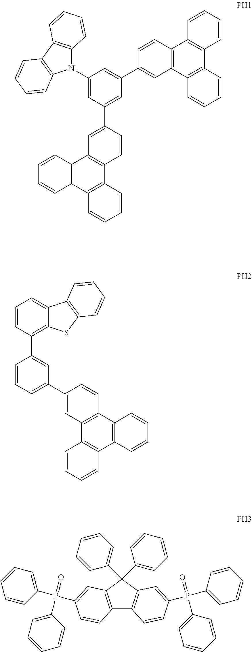
- a host material in the emission layer may include any one of the following Compounds PH1 to PH7:
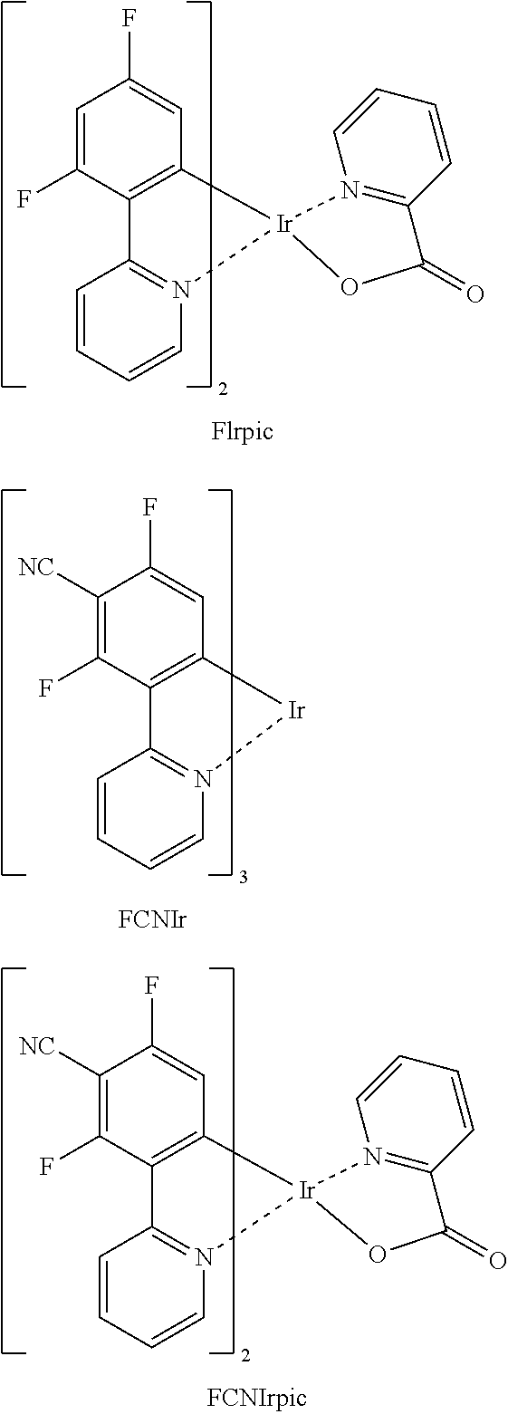
- the dopant in the emission layer may include an iridium complex.
- the dopant in the emission layer may include any one of the following compounds:
- the material having the triplet energy that is greater than that of the phosphorescent dopant may be included in a hole transport layer and may be represented by Formula 2 below:
- R 1 , R 2 , and R 4 are each independently selected from a hydrogen, a deuterium, —F, —Cl, —Br, —I, a cyano group, a substituted or unsubstituted C 6 -C 60 arylamino group, a substituted or unsubstituted C 1 -C 60 alkyl group, a substituted or unsubstituted C 3 -C 10 cycloalkyl group, a substituted or unsubstituted C 2 -C 10 heterocycloalkyl group, a substituted or unsubstituted C 3 -C 10 cycloalkenyl group, a substituted or unsubstituted C 2 -C 10 heterocycloalkenyl group, a substituted or unsubstituted C 6 -C 60 aryl group, a substituted or unsubstituted C 1 -C 60 heteroaryl group, a substituted or un
- the material having the triplet energy that is greater than that of the phosphorescent dopant may be included in an electron transport layer and may be represented by any one of Formulae 3 and 4: (A 21 ) n21 -(A 22 ) n22 -(A 23 ) n23 -(A 24 ) n24 ⁇ Formula 3>
- a 21 and A 24 are each independently selected from a substituted or unsubstituted C 6 -C 60 aryl group and a substituted or unsubstituted C 1 -C 60 heteroaryl group;
- a 22 and A 23 are each independently from a substituted or unsubstituted C 6 -C 60 arylene group, a substituted or unsubstituted C 1 -C 60 heteroarylene group, a substituted or unsubstituted divalent non-aromatic condensed polycyclic group, and a substituted or unsubstituted divalent non-aromatic condensed heteropolycyclic group;
- at least one of A 21 to A 24 is selected from a substituted or unsubstituted nitrogen atom-containing C 1 -C 60 heteroaryl or heteroarylene group;
- n21 to n24 are each independently selected from 0, 1, 2, and 3; and a sum of n21, n22, n23, and n24 is 4 or greater
- L 21 and L 22 are each independently selected from a substituted or unsubstituted alkylene group, a substituted or unsubstituted silylene group, a substituted or unsubstituted C 6 -C 60 arylene group, a substituted or unsubstituted C 1 -C 60 heteroarylene group, a substituted or unsubstituted divalent non-aromatic condensed polycyclic group, and a substituted or unsubstituted divalent non-aromatic condensed heteropolycyclic group; a21 and a22 are each independently integers selected from 0 to 3, and in the case of a21 or a22 being 2 or greater, each of L 21 or L 22 are identical to or different from each other; R 21 and R 22 are each independently selected from a hydrogen, a substituted or unsubstituted C 6 -C 60 aryl group, a substituted or unsubstituted C 1 -C 60 heteroaryl group
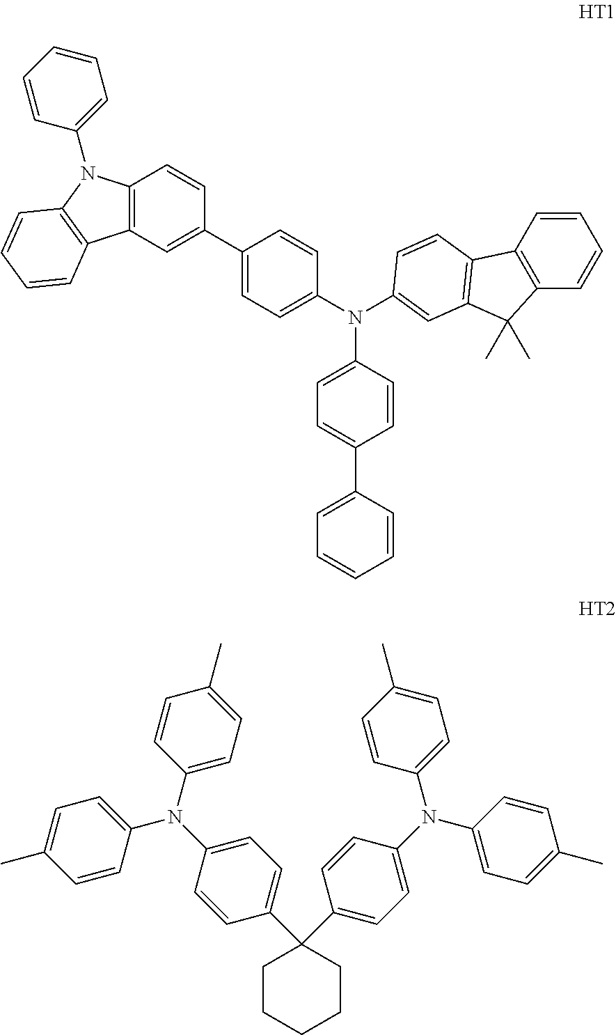
- the material having the triplet energy that is greater than that of the phosphorescent dopant may be included in a hole transport layer and may be one of Compound HT1 or Compound HT2, below:
- the material having the triplet energy that is greater than that of the phosphorescent dopant may be included in an electron transport layer and may be one of Compound ET1 or Compound ET2, below:
- the electron transport region may include a metal complex.
- the metal complex may include a lithium complex.
- the organic layer may be formed by a wet process.
- the embodiments may be realized by providing a flat display apparatus including a source electrode; a drain electrode; and the organic light-emitting device according to an embodiment, wherein the first electrode of the organic light-emitting device is electrically connected to the source electrode or the drain electrode.
- FIG. 1 illustrates a schematic view of an organic light-emitting device according to an embodiment.
- the term “and/or” includes any and all combinations of one or more of the associated listed items. Expressions such as “at least one of” when preceding a list of elements, modify the entire list of elements and do not modify the individual elements of the list.
- an organic light-emitting device may include a first electrode; a second electrode facing the first electrode; and an organic layer between the first electrode and the second electrode and including an emission layer.
- the organic layer may include i) a hole transport region that is between the first electrode and the emission layer and that includes at least one of a hole transport layer, a hole injection layer, and a buffer layer, and ii) an electron transport region that is between the emission layer and the second electrode and that includes at least one of a hole blocking layer, an electron transport layer, and an electron injection layer,
- the emission layer may include, e.g., as a material for forming the same, at least one host (H) and at least one phosphorescent dopant (D) of which an electron affinity (EA), and an ionization potential (IP) simultaneously satisfy relationships represented by Equations (1) and (2) below.
- the hole transport region and/or the electron transport region may include a layer that is adjacent to the emission layer and that includes a material having a triplet energy (T 1 ) that is greater than that of the phosphorescent dopant D.
- the triplet energy T 1 of the host H and/or the phosphorescent dopant D in the emission layer may satisfy the following relationship. T 1 ( H ) ⁇ T 1 ( D )
- the holes and the electrons may be directly injected to the dopant without passing through the host.
- the holes and the electrons may not be injected to the host that has a relatively high injection barrier, and driving voltage of the organic light-emitting device may be decreased.
- the carriers may be directly injected to the dopant, and the host may not need to have a greater triple energy T 1 than that of the dopant.
- T 1 triplet energy
- the host having a slightly low triplet energy T 1 e.g., T 1 ⁇ 0.3 eV, which may be low enough to enable a thermal activated energy transfer at room or ambient temperature, and that is, a triplet energy T 1 of the host may be transferred to that of the dopant.
- T 1 slightly low triplet energy
- T 1 e.g., T 1 ⁇ 0.3 eV, which may be low enough to enable a thermal activated energy transfer at room or ambient temperature, and that is, a triplet energy T 1 of the host may be transferred to that of the dopant.
- the carriers that are injected may be available.
- the efficiency of the organic light-emitting device may be decreased
- a material having a relatively small energy gap compared to other materials may be introduced to the organic light-emitting device, thereby obtaining diversity of materials to be developed.
- the layer including a material having a greater triplet energy T 1 than that of the phosphorescent dopant and being adjacent to the emission layer may be a hole transport layer and/or an electron transport layer.
- the material having a greater triplet energy T 1 than that of the phosphorescent dopant may have or include a carbazole framework or moiety, and may be included in the hole transport layer and/or the electron transport layer.
- At least one of the hole transport layer and the electron transport layer may include a material including a carbazole moiety.
- the host H and the phosphorescent dopant D in the emission layer may have a triplet energy T 1 satisfying a relationship represented by Equation (3) below.
- a thermal activated energy transfer may occur at ambient temperature, e.g., a triplet energy T 1 of the host may be transferred to that of the dopant.
- the carriers injected to the host may become available.
- the host H in the emission layer may have an electron affinity EA and an ionization potential IP satisfying a relationship represented by Equation (4) below.
- the host in the emission layer may be a compound represented by Formula 1 below.
- X may be selected from CR 3 R 4 , NR 5 , S, and O,
- Y 1 to Y 4 may each independently be selected from CR 6 and N,
- R 1 to R 6 may each independently be selected from a hydrogen, a deuterium, —F, —Cl, —Br, —I, a hydroxyl group, a cyano group, a nitro group, an amino group, an amidino group, a hydrazine group, a hydrazone group, a carboxylic acid or a salt thereof, a sulfonic acid or a salt thereof, a phosphoric acid or a salt thereof, a substituted or unsubstituted C 1 -C 60 alkyl group, a substituted or unsubstituted C 3 -C 10 cycloalkyl group, a substituted or unsubstituted C 2 -C 10 heterocycloalkyl group, a substituted or unsubstituted C 3 -C 10 cycloalkenyl group, a substituted or unsubstituted C 2 -C 10 heterocycloalkenyl group, a substituted or un
- At least one substituent of the substituted C 1 -C 60 alkyl group, the substituted C 3 -C 10 cycloalkyl group, the substituted C 2 -C 10 heterocycloalkyl group, the substituted C 3 -C 10 cycloalkenyl group, the substituted C 2 -C 10 heterocycloalkenyl group, the substituted C 6 -C 60 aryl group, the substituted C 2 -C 60 heteroaryl group, the substituted monovalent non-aromatic condensed polycyclic group, and the substituted monovalent non-aromatic condensed heteropolycyclic group may be selected from:
- a deuterium —F, —Cl, —Br, —I, a hydroxyl group, a cyano group, a nitro group, an amino group, an amidino group, a hydrazine group, a hydrazone group, a carboxylic acid or a salt thereof, a sulfonic acid or a salt thereof, a phosphoric acid or a salt thereof, a C 1 -C 60 alkyl group, a C 2 -C 60 alkenyl group, a C 2 -C 60 alkynyl group, and a C 1 -C 60 alkoxy group;
- Q 11 to Q 17 , Q 21 to Q 27 , and Q 31 to Q 37 may be each independently selected from a hydrogen, a deuterium, —F, —Cl, —Br, —I, a hydroxyl group, a cyano group, a nitro group, an amino group, an amidino group, a hydrazine group, a hydrazone group, a carboxylic acid or a salt thereof, a sulfonic acid or a salt thereof, a phosphoric acid or a salt thereof, a C 1 -C 60 alkyl group, a C 2 -C 60 alkenyl group, a C 2 -C 60 alkynyl group, a C 1 -C 60 alkoxy group, a C 3 -C 10 cycloalkyl group, a C 2 -C 10 heterocycloalkyl group, a C 3 -C 10 cycloalkenyl group, a C 2 -C 10 heterocycl
- n and n may each independently be an integer of 1 to 4. In the case of m or n being 2 or more, 2 or more of R 1 or R 2 may be identical to or different from each other.
- adjacent substituents or ones of R 1 to R 2 may be bound to each other to form a ring (e.g., or may be separate).
- the host material in the emission layer may include any one of Compounds PH1 to PH7, below.
- a dopant in the emission layer may include an iridium (Ir) complex.
- a dopant in the emission layer may be any one of the compounds or complexes below.
- At least one of the hole transport layer and the electron transport layer may include a material including a carbazole moiety, and may further include a compound represented by any one of Formulae 2 to 4 below, in addition to the material including a carbazole moiety.
- the material having the triplet energy T 1 that is greater than that of a phosphorescent dopant may be included in the hole transport layer, and the material may be a compound represented by Formula 2 below.
- R 1 , R 2 , and R 4 may each independently be selected from a hydrogen, a deuterium, —F, —Cl, —Br, —I, a cyano group, a substituted or unsubstituted C 6 -C 60 arylamino group, a substituted or unsubstituted C 1 -C 60 alkyl group, a substituted or unsubstituted C 3 -C 10 cycloalkyl group, a substituted or unsubstituted C 2 -C 10 heterocycloalkyl group, a substituted or unsubstituted C 3 -C 10 cycloalkenyl group, a substituted or unsubstituted C 2 -C 10 heterocycloalkenyl group, a substituted or unsubstituted C 6 -C 60 aryl group, a substituted or unsubstituted C 1 -C 60 heteroaryl group, a substituted or unsubstistit
- R 3 and L may each independently be selected from a substituted or unsubstituted C 3 -C 10 cycloalkylene group, a substituted or unsubstituted C 2 -C 10 heterocycloalkylene group, a substituted or unsubstituted C 3 -C 10 cycloalkenylene group, a substituted or unsubstituted C 2 -C 10 heterocycloalkenylene group, a substituted or unsubstituted C 6 -C 60 arylene group, a substituted or unsubstituted heteroarylene group, a substituted or unsubstituted divalent non-aromatic condensed polycyclic group, and a substituted or unsubstituted divalent non-aromatic condensed heteropolycyclic group.
- adjacent substituents or ones of R 1 to R 4 may be bound to each other to form a ring (e.g., or may be separate).
- n may be an integer of 1 to 3, and in the case of n being 2 or more, 2 or more of R 3 may be identical to or different from each other.
- the material having the triplet energy T 1 that is greater than that of a phosphorescent dopant may be included in the hole transport layer, and the material may be any one of Compounds HT1 or HT2, below.
- the material having the triplet energy T 1 that is greater than that of a phosphorescent dopant may be included in the electron transport layer, and the material may be a compound of any one of Formula 3 or Formula 4, below.
- a 21 and A 24 may each independently be selected from a substituted or unsubstituted C 6 -C 60 aryl group and a substituted or unsubstituted C 1 -C 60 heteroaryl group;
- a 22 and A 23 may each independently be selected from a substituted or unsubstituted C 6 -C 60 arylene group, a substituted or unsubstituted C 1 -C 60 heteroarylene group, a substituted or unsubstituted divalent non-aromatic condensed polycyclic group, and a substituted or unsubstituted divalent non-aromatic condensed heteropolycyclic group.
- At least one of A 21 to A 24 may be selected from a substituted or unsubstituted, nitrogen atom-containing C 1 -C 60 heteroaryl or heteroarylene group;
- n21 to n24 may each independently be selected from 0, 1, 2, and 3.
- a sum of n21, n22, n23, and n24 may not be 0. In an implementation, the sum of n21, n22, n23, and n24 may be 4 or more.
- L 21 and L 22 may each independently be selected from a substituted or unsubstituted C 1 -C 10 alkylene group, a substituted or unsubstituted silylene group, a substituted or unsubstituted C 6 -C 60 arylene group, a substituted or unsubstituted C 1 -C 60 heteroarylene group, a substituted or unsubstituted divalent non-aromatic condensed polycyclic group, and a substituted or unsubstituted divalent non-aromatic condensed heteropolycyclic group;
- a21 and a22 may each independently be selected from 0 to 3, and in the case of a21 or a22 being 2 or more, 2 or more of L 21 or L 22 may be identical to or different from each other;
- R 21 and R 22 may each independently be selected from a hydrogen, a substituted or unsubstituted C 6 -C 60 aryl group, a substituted or unsubstituted C 1 -C 60 heteroaryl group, a substituted or unsubstituted monovalent non-aromatic condensed polycyclic group, and a substituted or unsubstituted monovalent non-aromatic condensed heteropolycyclic group;
- X 21 may be selected from an oxygen atom, a sulfur atom, and a selenium atom
- Y 21 may be selected from a single bond, a substituted or unsubstituted C 6 -C 60 aryl group, a substituted or unsubstituted C 6 -C 60 arylene group, a substituted or unsubstituted C 1 -C 60 heteroaryl group, and a substituted or unsubstituted C 1 -C 60 heteroarylene group; and
- n11 may be selected from 1, 2, and 3.
- the material having a triplet energy T 1 that is greater than that of a phosphorescent dopant may be included in the electron transport layer, and the material may be any one of the following compounds.
- (an organic layer) includes at least one compound” used herein includes a case in which “(an organic layer) includes one condensed cyclic compound of Formula 1 or a case in which (an organic layer) includes two or more different condensed compounds of Formula 1”.
- organic layer refers to a single layer and/or a plurality of layers disposed between the first electrode and the second electrode of the organic light-emitting device.
- a material included in the “organic layer” is not limited to an organic material.
- FIG. 1 illustrates a schematic view of an organic light-emitting device 10 according to an embodiment.
- the organic light-emitting device 10 may include a first electrode 110 , an organic layer 150 , and a second electrode 190 .
- a substrate may be disposed under the first electrode 110 or on the second electrode 190 .
- the substrate may be a glass substrate or a transparent plastic substrate, each with excellent mechanical strength, thermal stability, transparency, surface smoothness, ease of handling, and water repellency.
- the first electrode 110 may be formed by, e.g., depositing or sputtering a material for forming the first electrode 110 , on the substrate.
- the material for forming the first electrode 110 may be selected from materials with a high work function to facilitate the hole injection.
- the first electrode 110 may be, e.g., a reflective electrode, a semi-transparent electrode, or a transparent electrode.
- the material for forming the first electrode 110 may be a transparent and highly conductive material, and examples thereof include indium tin oxide (ITO), indium zinc oxide (IZO), tin oxide (SnO 2 ), and zinc oxide (ZnO).
- the material for forming the first electrode 110 which is a semi-transparent electrode or a reflective electrode, may be at least one selected from magnesium (Mg), aluminum (Al), aluminum-lithium (Al—Li), calcium (Ca), magnesium-indium (Mg—In), and magnesium-silver (Mg—Ag).
- the first electrode 110 may have a single-layered structure or a multi-layered structure including two or more layers.
- the first electrode 110 may have a three-layered structure of ITO/Ag/ITO.
- the organic layer 150 may be on the first electrode 110 .
- the organic layer 150 may include an emission layer.
- the organic layer 150 may further include a hole transport region between the first electrode 110 and the emission layer and an electron transport region between the emission layer and the second electrode 190 .
- the hole transport region may include at least one of a hole transport layer (HTL), a hole injection layer (HIL), and a buffer layer
- the electron transport region may include at least one of a hole blocking layer (HBL), an electron transport layer (ETL), and an electron injection layer (EIL).
- the hole transport region may have a single-layered structure formed of a single material, a single-layered structure formed of a plurality of different materials, or a multi-layered structure having a plurality of layers formed of different materials.
- the hole transport region may have a single-layered structure formed of different materials, or a structure of HIL/HTL, a structure of HIL/HTL/buffer layer, a structure of HIL/buffer layer, a structure of HTL/buffer layer, or a structure of HIL/HTL/EBL, wherein layers of each structure are sequentially stacked on the first electrode 110 in this stated order.
- the HIL may be formed on the first electrode 110 by using various methods, such as vacuum deposition, spin coating, casting, a Langmuir-Blodgett method, an ink-jet printing, a laser-printing, or a laser induced thermal imaging (LITI) method.
- various methods such as vacuum deposition, spin coating, casting, a Langmuir-Blodgett method, an ink-jet printing, a laser-printing, or a laser induced thermal imaging (LITI) method.
- the deposition may be performed, e.g., at a deposition temperature of about 100° C. to about 500° C., at a vacuum degree of about 10 ⁇ 8 torr to about 10 ⁇ 3 torr, and a deposition rate of about 0.01 ⁇ /sec to about 100 ⁇ /sec in consideration of a compound for forming the HIL to be deposited and a structure of the HIL to be formed.
- the coating may be performed, e.g., at a coating speed of about 2,000 rpm to about 5,000 rpm and at a temperature of about 80° C. to about 200° C., in consideration of a compound for forming the HIL to be deposited and a structure of the HIL to be formed.
- the HTL may be formed on the first electrode 110 or on the HIL by using various methods, such as vacuum deposition, spin coating, casting, an LB method, an ink-jet printing, a laser-printing, or an LITI method.
- the deposition and coating conditions for the HTL may be determined by referring to the deposition and coating conditions for the HIL.
- the hole transport region may include a layer including a material that has a triplet energy T 1 that is greater than that of a phosphorescent dopant, and the layer may be adjacent to the emission layer.
- the layer may be, e.g., an HTL.
- a thickness of the hole transport region may be about 100 ⁇ to about 10,000 ⁇ , e.g., about 100 ⁇ to about 1,000 ⁇ .
- a thickness of the HIL may be about 100 ⁇ to about 10,000 ⁇ , e.g., about 100 ⁇ to about 1,000 ⁇
- a thickness of the HTL may be about 50 ⁇ to about 2,000 ⁇ , e.g., about 100 ⁇ to about 1,500 ⁇ .
- the hole transport region may further include, in addition to these materials, a charge-generation material for the improvement of conductivity.
- the charge-generation material may be homogeneously or non-homogeneously dispersed in the hole transport region.
- the charge-generation material may be, e.g., a p-dopant.
- the p-dopant may include, e.g., one of a quinone derivative, a metal oxide, and a cyano group-containing compound.
- examples of the p-dopant may include a quinone derivative, such as tetracyanoquinonedimethane (TCNQ), and 2,3,5,6-tetrafluoro-tetracyano-1,4-benzoquinonedimethane (F4-TCNQ); a metal oxide, such as a tungsten oxide and a molybdenum oxide; and Compound HT-D1 below.
- the hole transport region may further include, in addition to the EBL, the HIL, and the HTL, a buffer layer.
- the buffer layer may help compensate for an optical resonance distance according to a wavelength of light emitted from the emission layer, and thus, a light-emission efficiency of a formed organic light-emitting device may be improved.
- the materials for forming the hole transport region may be used.
- the EBL may prevent electron injection from the electron transport region.
- the emission layer may be formed on the first electrode 110 or on the hole transport region by using various methods, such as vacuum deposition, spin coating, casting, an LB method, an ink-jet printing, a laser-printing, or an LITI method.
- the deposition and coating conditions for forming the emission layer may be determined by referring to the deposition and coating conditions for forming the HIL.
- the emission layer may be patterned into a red emission layer, a green emission layer, and a blue emission layer, according to a sub-pixel.
- the emission layer may have a stacked structure of a red emission layer, a green emission layer, and a blue emission layer, or may include a red light emission material, a green light emission material, and a blue light emission material, which are mixed with each other in a single layer, to emit white light.
- the emission layer may include a host and a dopant.
- the host (H) and the dopant (D) may have an electron affinity EA and an ionization potential IP simultaneously satisfying the relationships of Equation (1) and Equation (2) below.
- the host may include, in addition to a compound satisfying the relationships of Equations 1 and 2, above, at least one other material, e.g., TPBi, CBP, CDBP and TCP below.
- at least one other material e.g., TPBi, CBP, CDBP and TCP below.
- the host may include a compound represented by Formula 301 below.
- Ar 301 may be selected from:
- naphthalene a heptalene, a fluorene, a spiro-fluorene, a benzofluorene, a dibenzofluorene, a phenalene, a phenanthrene, a fluoranthene, and a triphenylene;
- L 301 may be understood by referring to the description provided in connection with L;
- R 301 may be selected from:
- a C 1 -C 20 alkyl group and a C 1 -C 20 alkoxy group each substituted with at least one of a deuterium, —F, —Cl, —Br, —I, a hydroxyl group, a cyano group, a nitro group, an amino group, an amidino group, a hydrazine group, a hydrazone group, a carboxylic acid or a salt thereof, a sulfonic acid or a salt thereof, a phosphoric acid or a salt thereof, a phenyl group, a naphthyl group, a fluorenyl group, a spiro-fluorenyl group, a benzofluorenyl group, a phenanthrenyl group, a pyridinyl group, a pyrazinyl group, a pyrimidinyl group, a pyridazinyl group, a quinolinyl group,
- xb1 may be selected from 0, 1, 2, and 3;
- xb2 may be selected from 1, 2, 3, and 4.
- L 301 may be selected from:
- a phenylene group a naphthylene group, a fluorenylene group, a spiro-fluorenylene group, a benzofluorenylene group, a dibenzofluorenylene group, a phenanthrenylene group;
- the dopant may include, in addition to a compound satisfying the relationships above, at least one other material, e.g., a fluorescent dopant or a phosphorescent dopant.
- the phosphorescent dopant may include an organometallic complex represented by Formula 401 below.
- M may be selected from iridium (Ir), platinum (Pt), osmium (Os), titanium (Ti), zirconium (Zr), hafnium (Hf), europium (Eu), terbium (Tb), and thulium (Tm);
- X 401 to X 404 may each independently be selected from nitrogen or carbon;
- rings A 401 and A 402 may each independently be selected from a substituted or unsubstituted benzene, a substituted or unsubstituted naphthalene, a substituted or unsubstituted fluorene, a substituted or unsubstituted spiro-fluorene, a substituted or unsubstituted indene, a substituted or unsubstituted pyrrole, a substituted or unsubstituted thiophene, a substituted or unsubstituted furan, a substituted or unsubstituted imidazole, a substituted or unsubstituted pyrazole, a substituted or unsubstituted thiazole, a substituted or unsubstituted isothiazole, a substituted or unsubstituted oxazole, a substituted or unsubstituted isoxazole, a substituted or unsubsti
- the substituted benzene at least one substituent of the substituted benzene, the substituted naphthalene, the substituted fluorene, the substituted spiro-fluorene, the substituted indene, the substituted pyrrole, the substituted thiophene, the substituted furan, the substituted imidazole, the substituted pyrazole, the substituted thiazole, the substituted isothiazole, the substituted oxazole, the substituted isoxazole, the substituted pyridine, the substituted pyrazine, the substituted pyrimidine, the substituted pyridazine, the substituted quinoline, the substituted isoquinoline, the substituted benzoquinoline, the substituted quinoxalaine, the substituted quinazoline, the substituted carbazole, the substituted benzoimidazole, the substituted benzofuran, the substituted benzothiophene, the substituted isobenzothiophene,
- a deuterium —F, —Cl, —Br, —I, a hydroxyl group, a cyano group, a nitro group, an amino group, an amidino group, a hydrazine group, a hydrazone group, a carboxylic acid or a salt thereof, a sulfonic acid or a salt thereof, a phosphoric acid or a salt thereof, a C 1 -C 60 alkyl group, a C 2 -C 60 alkenyl group, a C 2 -C 60 alkynyl group, and a C 1 -C 60 alkoxy group;
- L 401 may be an organic ligand
- xc1 may be 1, 2, or 3;
- xc2 may be 0, 1, 2, or 3.
- L 401 may be a monovalent, divalent, or trivalent organic ligand.
- L 401 may be selected from a halogen ligand (for example, Cl or F), a diketone ligand (for example, acetylacetonate, 1,3-diphenyl-1,3-propandionate, 2,2,6,6-tetramethyl-3,5-heptandionate, or hexafluoroacetonate), a carboxylic acid ligand (for example, picolinate, dimethyl-3-pyrazolecarboxylate, or benzoate), a carbon mono-oxide ligand, an isonitrile ligand, a cyano ligand, and a phosphorous ligand (for example, phosphine and phosphaite).
- a halogen ligand for example, Cl or F
- a diketone ligand for example, acetylacetonate, 1,3-diphenyl-1,3
- a 401 in Formula 401 has 2 or more substituents
- the 2 or more substituents of A 401 may be bound to each other to form a saturated or unsaturated ring.
- a 402 in Formula 401 has 2 or more substituents
- the 2 or more substituents of A 402 may be bound to each other to form a saturated or unsaturated ring.
- a 401 and A 402 may be respectively directly connected to A 401 and A 402 of other neighboring ligands with or without a linking group (for example, a C 1 -C 5 alkylene group or —N(R′)— (wherein R′ may be a C 1 -C 10 alkyl group or a C 6 -C 20 aryl group), or —C( ⁇ O)—).
- a linking group for example, a C 1 -C 5 alkylene group or —N(R′)— (wherein R′ may be a C 1 -C 10 alkyl group or a C 6 -C 20 aryl group), or —C( ⁇ O)—).
- the phosphorescent dopant may include, e.g., at least one of Compounds PD1 to PD74 below.
- the phosphorescent dopant may include PtOEP below:
- An amount of the dopant included in the emission layer may be, e.g., about 0.01 parts to about 30 parts by weight, based on 100 parts by weight of the host.
- a thickness of the emission layer may be about 100 ⁇ to about 1,000 ⁇ , e.g., about 200 ⁇ to about 600 ⁇ . When the thickness of the emission layer is within this range, excellent light emission characteristics may be obtained without a substantial increase in driving voltage.
- the electron transport region may be disposed on the emission layer.
- the electron transport region may include, e.g., at least one of an HBL, an ETL, and an EIL.
- the electron transport region may have a structure of ETL/EIL or a structure of HBL/ETL/EIL, wherein layers of each structure are sequentially stacked on the emission layer in the stated order.
- the organic layer 150 may include the electron transport region between the emission layer and the second electrode 190 .
- the electron transport region may include a layer including a material that has a triplet energy T 1 that is greater than that of a phosphorescent dopant, and the layer may be adjacent to the emission layer.
- the layer may be, e.g., an ETL.
- the electron transport region may include an HBL.
- the HBL may be formed to help prevent diffusion of triplet excitons or holes into the ETL.
- the HBL may be formed on the emission layer by using various methods, such as vacuum deposition, spin coating casting, an LB method, an ink-jet printing, a laser-printing, or an LITI method.
- deposition and coating conditions for forming the HBL may be determined by referring to the deposition and coating conditions for forming the HIL.
- the HBL may include, e.g., at least one of BCP and Bphen below.
- a thickness of the HBL may be about 20 ⁇ to about 1,000 ⁇ , e.g., about 30 ⁇ to about 300 ⁇ . When the thickness of the HBL is within these ranges, excellent hole blocking characteristics may be obtained without a substantial increase in driving voltage.
- the electron transport region may include an ETL, and the ETL may be formed on the emission layer or on the HBL by using various methods, such as vacuum deposition, spin coating casting, an LB method, an ink-jet printing, a laser-printing, or an LITI method.
- the deposition and coating conditions for the ETL may be determined by referring to the deposition and coating conditions for forming the HIL.
- the organic layer 150 may include the electron transport region between the emission layer and the second electrode 190 , and the electron transport region may include an ETL.
- the ETL may include a plurality of layers.
- the electron transport region may include a first ETL and a second ETL.
- the ETL may further include, e.g., at least one of BCP, Bphen, and Alq 3 , Balq, TAZ, and NTAZ below.
- a thickness of the ETL may be about 100 ⁇ to about 1,000 ⁇ , e.g., about 150 ⁇ to about 500 ⁇ . When the thickness of ETL is within these ranges, satisfactory electron transporting characteristics may be obtained without a substantial increase in driving voltage.
- the ETL may further include, in addition to the materials described above, a metal-containing material.
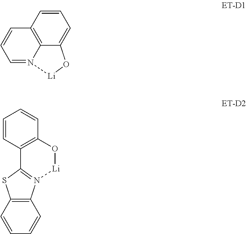
- the metal-containing material may include a lithium (Li) complex.
- the Li complex may include, e.g., Compound ET-D1 (lithium quinolate, LiQ) or ET-D2 below.
- the electron transport region may include an EIL that facilitates the electron injection from the second electrode 190 .
- the EIL may be formed on the ETL by using various methods, such as vacuum deposition, spin coating casting, an LB method, an ink-jet printing, a laser-printing, or an LITI method.
- the deposition and coating conditions for the EIL may be determined by referring to the deposition and coating conditions for the HIL.
- the EIL may include at least one selected from LiF, NaCl, CsF, Li 2 O, BaO, and LiQ.
- a thickness of the EIL may be about 1 ⁇ to about 100 ⁇ , e.g., about 3 ⁇ to about 90 ⁇ . When the thickness of the EIL is within these ranges, satisfactory electron transporting characteristics may be obtained without a substantial increase in driving voltage.
- the second electrode 190 may be disposed on the organic layer 150 .
- the second electrode 190 may be a cathode that is an electron injection electrode.
- a material for forming the second electrode 190 may be a material having a low work function, and examples thereof may include a metal, an alloy, an electrically conductive compound, or a mixture thereof.
- Examples of the material for forming the second electrode 190 may include lithium (Li), magnesium (Mg), aluminum (Al), aluminum-lithium (Al—Li), calcium (Ca), magnesium-indium (Mg—In), and magnesium-silver (Mg—Ag).
- the material for forming the second electrode 190 may include ITO or IZO.
- the second electrode 190 may be a reflective electrode, a semi-transmissive electrode, or a transmissive electrode.
- the organic layer 150 of the organic light-emitting device 10 may be formed by vacuum deposition using a compound according to an embodiment, or by a wet method including coating a compound prepared as solution according to an embodiment.
- An organic light-emitting device may be loaded onto various types of flat display devices, e.g., a passive matrix organic light-emitting display device and an active matrix organic light-emitting display device.
- a first electrode provided on the substrate may be electrically connected to a source electrode or a drain electrode of a thin film transistor as a pixel electrode.
- the organic light-emitting device may be provided in a flat display device that may display images on both sides.
- the C 1 -C 60 alkyl group refers to a linear or branched aliphatic C 1 -C 60 hydrocarbon monovalent group, and detailed examples thereof include a methyl group, an ethyl group, a propyl group, an isobutyl group, a sec-butyl group, a ter-butyl group, a pentyl group, an iso-amyl, and a hexyl group.
- the C 1 -C 60 alkylene group refers to a divalent group having the same structure as the C 1 -C 60 alkyl group.
- the C 1 -C 60 alkoxy group refers to a monovalent group having a formula of —OA 101 (wherein A 101 is the C 1 -C 60 alkyl group), and detailed examples thereof include a methoxy group, an ethoxy group, and an isopropyloxy group.
- the C 2 -C 60 alkenyl group refers to a hydrocarbon group formed by substituting at least one carbon double bond in the middle or terminal of the C 2 -C 60 alkyl group, and detailed examples thereof include an ethenyl group, a prophenyl group, and a butenyl group.
- the C 2 -C 60 alkenylene group refers to a divalent group having the same structure as the C 2 -C 60 alkenyl group.
- the C 2 -C 60 alkynyl group refers to a hydrocarbon group formed by substituting at least one carbon triple bond in the middle or terminal of the C 2 -C 60 alkyl group, and detailed examples thereof include an ethynyl group and a propynyl group.
- the C 2 -C 60 alkynylene group refers to a divalent group having the same structure as the C 2 -C 60 alkynyl group.
- the C 3 -C 10 cycloalkyl group refers to a saturated C 3 -C 10 monovalent hydrocarbon monocyclic group, and detailed examples thereof include a cyclopropyl group, a cyclobutyl group, a cyclopentyl group, a cyclohexyl group, and a cycloheptyl group.
- the C 3 -C 10 cycloalkylene group refers to a divalent group having the same structure as the C 3 -C 10 cycloalkyl group.
- the C 2 -C 10 heterocycloalkyl group refers to a C 2 -C 10 monovalent monocyclic group including at least one heteroatom selected from N, O, P, and S as a ring-forming atom, and detailed examples thereof include a tetrahydrofuranyl group and a tetrahydrothiophenyl group.
- the C 2 -C 10 heterocycloalkylene group refers to a divalent group having the same structure as the C 2 -C 10 heterocycloalkyl group.
- the C 3 -C 10 cycloalkenyl group refers to a C 3 -C 10 monovalent monocyclic group that has at least one double bond in a ring, but does not have aromacity, and detailed examples thereof include a cyclopentenyl group, a cyclohexenyl group, and a cycloheptenyl group.
- the C 3 -C 10 cycloalkenylene group refers to a divalent group having the same structure as the C 3 -C 10 cycloalkenyl group.
- the C 2 -C 10 heterocycloalkenyl group refers to a C 2 -C 10 monovalent monocyclic group including at least one heteroatom selected from N, O, P, and S as a ring-forming atom, and includes at least one double bond in a ring.
- Detailed examples of the C 2 -C 10 heterocycloalkenyl group include a 2,3-hydrofuranyl group and a 2,3-hydrothiophenyl group.
- the C 2 -C 10 heterocycloalkenylene group refers to a divalent group having the same structure as the C 2 -C 10 heterocycloalkenyl group.
- the C 6 -C 60 aryl group refers to C 6 -C 60 monovalent group having a carbocyclic aromatic system
- the C 6 -C 60 arylene group refers to a divalent group having a C 6 -C 60 carbocyclic aromatic system.
- the C 6 -C 60 aryl group include a phenyl group, a naphthyl group, an anthracenyl group, a phenanthrenyl group, a pyrenyl group, and a chrysenyl group.
- the C 6 -C 60 aryl group and the C 6 -C 60 arylene group include 2 or more rings, the 2 or more rings may be fused to each other.
- the C 2 -C 60 heteroaryl group refers to a monovalent group having a C 2 -C 60 carbocyclic aromatic system including at least one heteroatom selected from N, O, P, and S as a ring-forming atom
- the C 2 -C 60 heteroarylene group refers to a divalent group having a C 2 -C 60 carbocyclic aromatic system including at least one heteroatom selected from N, O, P, and S.
- C 2 -C 60 heteroaryl group examples include a pyridinyl group, a pyrimidinyl group, a pyrazinyl group, a pyridazinyl group, a triazinyl group, a quinolinyl group, and an isoquinolinyl group.
- the C 2 -C 60 heteroaryl group and the C 2 -C 60 heteroarylene group include 2 or more rings, the 2 or more rings may be fused to each other.
- the C 6 -C 60 aryloxy group indicates to —OA 102 (wherein, A 102 is the C 6 -C 60 aryl group), and the C 6 -C 60 arylthio group indicates —SA 103 (wherein, A 103 is the C 6 -C 60 aryl group).
- the monovalent non-aromatic condensed polycyclic group refers to a monovalent group having 2 or more rings that are fused to each other, including only carbon as a ring forming atom (for example, carbon number may be 8 to 60), wherein the entire molecule does not have aromaticity.
- Detailed examples of the monovalent non-aromatic condensed polycyclic group include a fluorenyl group or the like.
- the divalent non-aromatic condensed polycyclic group refers to a divalent group having the same structure as the monovalent non-aromatic condensed polycyclic group.
- the monovalent non-aromatic condensed heteropolycyclic group refers to a monovalent group having 2 or more rings that are fused to each other, including a heteroatom selected from N, O, P, and S as a ring-forming atom, in addition to carbon (for example, carbon number may be 2 to 60), wherein the entire molecule does not have aromaticity.
- the monovalent non-aromatic condensed heteropolycyclic group includes a carbazolyl group or the like.
- the divalent non-aromatic condensed heteropolycyclic group refers to a divalent group having the same structure as the monovalent non-aromatic hetero-condensed polycyclic group.
- a deuterium —F, —Cl, —Br, —I, a hydroxyl group, a cyano group, a nitro group, an amino group, an amidino group, a hydrazine group, a hydrazone group, a carboxylic acid or a salt thereof, a sulfonic acid or a salt thereof, a phosphoric acid or a salt thereof, a C 1 -C 60 alkyl group, a C 2 -C 60 alkenyl group, a C 2 -C 60 alkynyl group and C 1 -C 60 alkoxy group;
- Q 1 to Q 7 , Q 11 to Q 17 , Q 21 to Q 27 , and Q 31 to Q 37 may be each independently selected from a hydrogen, a deuterium, —F, —Cl, —Br, —I, a hydroxyl group, a cyano group, a nitro group, an amino group, an amidino group, a hydrazine group, a hydrazone group, a carboxylic acid or a salt thereof, a sulfonic acid or a salt thereof, a phosphoric acid or a salt thereof, a C 1 -C 60 alkyl group, a C 2 -C 60 alkenyl group, a C 2 -C 60 alkynyl group, a C 1 -C 60 alkoxy group, a C 3 -C 10 cycloalkyl group, a C 2 -C 10 heterocycloalkyl group, a C 3 -C 10 cycloalkenyl group, a C 3
- a deuterium —F, —Cl, —Br, —I, a hydroxyl group, a cyano group, a nitro group, an amino group, an amidino group, a hydrazine group, a hydrazone group, a carboxylic acid or a salt thereof, a sulfonic acid or a salt thereof, a phosphoric acid or a salt thereof, a C 1 -C 60 alkyl group, a C 2 -C 60 alkenyl group, a C 2 -C 60 alkynyl group, and C 1 -C 60 alkoxy group;
- a cyclopentyl group a cyclohexyl group, a cycloheptyl group, a cyclopentenyl group, a cyclohexenyl group, a phenyl group, a pentalenyl group, an indenyl group, a naphthyl group, an azulenyl group, a heptalenyl group, an indacenyl group, an acenaphthyl group, a fluorenyl group, a spiro-fluorenyl group, a benzofluorenyl group, a dibenzofluorenyl group, a phenalenyl group, a phenanthrenyl group, an anthracenyl group, a fluoranthenyl group, a triphenylenyl group, a pyrenyl group, a chrysenyl group, a naphthacenyl group
- a cyclopentyl group a cyclohexyl group, a cycloheptyl group, a cyclopentenyl group, a cyclohexenyl group, a phenyl group, a pentalenyl group, an indenyl group, a naphthyl group, an azulenyl group, a heptalenyl group, an indacenyl group, an acenaphthyl group, a fluorenyl group, a spiro-fluorenyl group, a benzofluorenyl group, a dibenzofluorenyl group, a phenalenyl group, a phenanthrenyl group, an anthracenyl group, a fluoranthenyl group, a triphenylenyl group, a pyrenyl group, a chrysenyl group, a naphthacenyl group
- Q 1 to Q 7 , Q 11 to Q 17 , Q 21 to Q 27 , and Q 31 to Q 37 may be each independently selected from a hydrogen, a deuterium, —F, —Cl, —Br, —I, a hydroxyl group, a cyano group, a nitro group, an amino group, an amidino group, a hydrazine group, a hydrazone group, a carboxylic acid or a salt thereof, a sulfonic acid or a salt thereof, a phosphoric acid or a salt thereof, a C 1 -C 60 alkyl group, a C 2 -C 60 alkenyl group, a C 2 -C 60 alkynyl group, a C 1 -C 60 alkoxy group, a cyclopentyl group, a cyclohexyl group, a cycloheptyl group, a cyclopentenyl group, a cyclohexenyl group
- Ph refers to a phenyl group
- Me refers to a methyl group
- Et refers to an ethyl group
- ter-Bu or “Bu t ” used herein refers to a tert-butyl group.
- ITO glass substrate was cut into a size of 50 mm ⁇ 50 mm ⁇ 0.5 mm, ultrasonically washed with acetone, isopropyl alcohol, and pure water each for 15 minutes, and cleaned by exposure to ultraviolet rays for 30 minutes and then to ozone.
- Compound HT1 was vacuum deposited on the ITO glass substrate to form an HTL having a thickness of 600 ⁇ , and Compound PH1 (as a host) and 5 wt % FIrpic (as a dopant) were vacuum co-deposited on the HTL to form an emission layer having a thickness of 300 ⁇ . Thereafter, Compound ET1 and Liq were co-deposited at a weight ratio of 5:5 on the emission layer to form an ETL having a thickness of 400 ⁇ . Liq and Al were sequentially vacuum deposited thereon as an EIL into a thickness of 10 ⁇ and as a cathode into a thickness of 2,000 ⁇ , respectively, to thereby manufacture an organic light-emitting device.
- An organic light-emitting device was manufactured in the same manner as in Example 1, except that Compound PH2 was used instead of Compound PH1 as a host material.
- an organic light-emitting device including a structure of ITO/HT1 (600 ⁇ )/PH2+5% FIrpic (300 ⁇ )/ET1+Liq (400 ⁇ )/Liq (10 ⁇ )/Al (2,000 ⁇ ) was manufactured.
- An ITO glass substrate was cut into a size of 50 mm ⁇ 50 mm, ultrasonically washed with acetone, isopropyl alcohol, and pure water each for 15 minutes, and cleaned by exposure to ultraviolet rays for 30 minutes and then to ozone. Then, Compound HT2 was vacuum deposited on the ITO glass substrate to form an HTL having a thickness of 600 ⁇ , and Compound PH3 (as a host) and 5 wt % FCNIr (as a dopant) were vacuum co-deposited on the HTL to form an emission layer having a thickness of 300 ⁇ .
- Compound ET2 was vacuum deposited on the emission layer having a thickness of 50 ⁇ to form a first electron transport layer, and Alq 3 was vacuum deposited on the first electron transport layer to form a second ETL having a thickness of 350 ⁇ .
- Liq and Al were sequentially vacuum deposited thereon as an EIL into a thickness of 10 ⁇ and a cathode into a thickness of 2,000 ⁇ , respectively, to thereby manufacture an organic light-emitting device.
- An organic light-emitting device was manufactured in the same manner as in Example 3, except that Compound PH4 was used instead of Compound PH3 as a host material. That is, an organic light-emitting device including a structure of ITO/HT2 (600 ⁇ )/PH4+5% FCNIr (300 ⁇ )/ET2 (50 ⁇ )/Alq 3 (350 ⁇ )/Liq (10 ⁇ )/Al (2,000 ⁇ ) was manufactured.
- An organic light-emitting device was manufactured in the same manner as in Example 3, except that Compound PH5 was used instead of Compound PH3 as a host material. That is, an organic light-emitting device including a structure of ITO/HT2 (600 ⁇ )/PH5+5% FCNIr (300 ⁇ )/ET2 (50 ⁇ )/Alq 3 (350 ⁇ )/Liq (10 ⁇ )/Al (2,000 ⁇ ) was manufactured.
- An organic light-emitting device was manufactured in the same manner as in Example 3, except that Compound PH6 was used instead of Compound PH3 as a host material and that FCNIrpic was used instead of FCNIr as a dopant material. That is, an organic light-emitting device including a structure of ITO/HT2 (600 ⁇ )/PH6+5% FCNIrpic (300 ⁇ )/ET2 (50 ⁇ )/Alq 3 (350 ⁇ )/Liq (10 ⁇ )/Al (2,000 ⁇ ) was manufactured.
- An organic light-emitting device was manufactured in the same manner as in Example 6, except that Compound PH7 was used instead of PH6 as a host material. That is, an organic light-emitting device including a structure of ITO/HT2 (600 ⁇ )/PH7+5% FCNIrpic (300 ⁇ )/ET2 (50 ⁇ )/Alq 3 (350 ⁇ )/Liq (10 ⁇ )/Al (2,000 ⁇ ) was manufactured.
- An organic light-emitting device was manufactured in the same manner as in Example 1, except that Compound PH8 was used instead of Compound PH1 as a host material. That is, an organic light-emitting device including a structure of ITO/HT1 (600 ⁇ )/PH8+5% FIrpic (300 ⁇ )/ET1+Liq (400 ⁇ )/Liq (10 ⁇ )/Al (2,000 ⁇ ) was manufactured.
- An organic light-emitting device was manufactured in the same manner as in Example 3, except that Compound PH2 was used instead of Compound PH3 as a host material. That is, an organic light-emitting device including a structure of ITO/HT2 (600 ⁇ )/PH2+5% FCNIr (300 ⁇ )/ET2 (50 ⁇ )/Alq 3 (350 ⁇ )/Liq (10 ⁇ )/Al (2,000 ⁇ ) was manufactured.
- An organic light-emitting device was manufactured in the same manner as in Example 1, except that Compound PH7 was used instead of Compound PH1 as a host material. That is, an organic light-emitting device including a structure of ITO/HT1 (600 ⁇ )/PH7+5% FIrpic (300 ⁇ )/ET1+Liq (400 ⁇ )/Liq (10 ⁇ )/Al (2,000 ⁇ ) was manufactured.
- An organic light-emitting device was manufactured in the same manner as in Example 3, except that Compound PH9 was used instead of Compound PH3. That is, an organic light-emitting device having a structure of ITO/HT2 (600 ⁇ )/PH9+5% FCNIr (300 ⁇ )/ET2 (50 ⁇ )/Alq 3 (350 ⁇ )/Liq (10 ⁇ )/Al (2,000 ⁇ ) was manufactured.
- An organic light-emitting device was manufactured in the same manner as in Example 1, except that Compound PH10 was used instead of Compound PH1 as a host material. That is, an organic light-emitting device having a structure of ITO/HT1 (600 ⁇ )/PH10+5% FIrpic (300 ⁇ )/ET1+Liq (400 ⁇ )/Liq (10 ⁇ )/Al (2,000 ⁇ ) was manufactured.
- An organic light-emitting device was manufactured in the same manner as in Example 6, except that Compound PH10 was used instead of PH6 as a host material. That is, an organic light-emitting device having a structure of ITO/HT2 (600 ⁇ )/PH10+5% FCNIrpic (300 ⁇ )/ET2 (50 ⁇ )/Alq 3 (350 ⁇ )/Liq (10 ⁇ )/Al (2,000 ⁇ ) was manufactured.
- Comparative Example 7 In the Case of Including a Material Having a Low T 1 in the HTL
- An organic light-emitting device was manufactured in the same manner as in Example 1, except that NPB was used instead of HT1 as a material for forming the HTL. That is, an organic light-emitting device having a structure of ITO/NPB (600 ⁇ )/PH1+5% FIrpic (300 ⁇ )/ET1+Liq (400 ⁇ )/Liq (10 ⁇ )/Al (2,000 ⁇ ) was manufactured.
- Comparative Example 8 In the Case of Including a Material Having a Low T 1 in the ETL
- An organic light-emitting device was manufactured in the same manner as in Example 1, except that Alq 3 was used instead of ET1 and Liq as a material for forming the ETL. That is, an organic light-emitting device having a structure of ITO/HT1 (600 ⁇ )/PH1+5% FIrpic (300 ⁇ )/Alq 3 (400 ⁇ )/Liq (10 ⁇ )/Al (2,000 ⁇ ) was manufactured.
- Comparative Example 9 In the Case of Including a Material Having a Low T 1 in Both the HTL and the ETL
- An organic light-emitting device was manufactured in the same manner as in Example 1, except that Alq 3 was used instead of ET1 and Liq as a material for forming the ETL and that NPB was used instead of HT1 as a material for forming the HTL. That is, an organic light-emitting device having a structure of ITO/NPB (600 ⁇ )/PH1+5% FIrpic (300 ⁇ )/Alq 3 (400 ⁇ )/Liq (10 ⁇ )/Al (2,000 ⁇ ) was manufactured.
- an organic light-emitting device when an organic light-emitting device uses a phosphorescent luminescent material, such an organic light-emitting device may be manufactured as a device having higher light emission efficiency than a device using a fluorescent material.
- a phosphorescent luminescent material may be suitable in terms of light emission characteristics, but in order to ideally achieve high light emission efficiency, efficiently confining energy in an emission layer in which the energy is excited may be desirable.
- a material having a high triplet energy T 1 may be used in a layer that is adjacent to the emission layer.
- a phosphorescent host may have a greater triplet energy T 1 than that of a dopant.
- a host molecule may increase an energy gap, and accordingly, the host molecule may have a high ionization potential IP and a low electron affinity EA.
- the organic light-emitting device may increase driving voltage, decrease light emission efficiency, and accordingly, degrade light emission lifespan.
- a material that has a greater triplet energy T 1 than that of the phosphorescent dopant may be employed as a phosphorescent host material.
- a material with a wide band gap may be suitable as a host.
- an organic compound having a wide gap between a single energy S 1 and a triplet energy T 1 may not be suitable as a host, e.g., because a carrier injection barrier of the organic compound may be increased.
- the material may be limitedly designed to reduce a conjugation length thereof, and accordingly, introduction of beneficial substituents may be restricted therewith.
- the embodiments complement the restriction and suggest a configuration that facilitates the carrier injection and decreases driving voltage of the organic light-emitting device.
- the embodiments may provide an organic light-emitting device capable of preventing a decrease in light emission efficiency and light emission lifespan.
- an organic light-emitting device As described above, in an organic light-emitting device according to an embodiment, electrons provided from a negative electrode and holes provided from a positive electrode may be recombined in an emission layer to produce excitons.
- the organic light-emitting device may be capable of preventing the occurrence of leakage current that may otherwise be caused by the holes or the electrons leaking to a layer that is adjacent to the emission layer, and accordingly, may also capable be of preventing a decrease in light emission efficiency and light emission lifespan.
Landscapes
- Physics & Mathematics (AREA)
- Chemical & Material Sciences (AREA)
- Engineering & Computer Science (AREA)
- Materials Engineering (AREA)
- Spectroscopy & Molecular Physics (AREA)
- Optics & Photonics (AREA)
- Organic Chemistry (AREA)
- Electroluminescent Light Sources (AREA)
Abstract
EA(D)−EA(H)≧0.2 eV (1)
IP(H)−IP(D)≧0.2 eV (2).
Description
EA(D)−EA(H)≧0.2 eV (1)
IP(H)−IP(D)≧0.2 eV (2), and
T 1(D)−T 1(H)≦0.3 eV (3).
IP(H)−EA(H)≦3.8 eV (4).


(A21)n21-(A22)n22-(A23)n23-(A24)n24 <Formula 3>


EA(D)−EA(H)≧0.2 eV (1)
IP(H)−IP(D)≧0.2 eV (2)
T 1(H)≦T 1(D)
T 1(D)−T 1(H)≦0.3 eV (3)
IP(H)−EA(H)≦3.8 eV (4)


(A21)n21-(A22)n22-(A23)n23-(A24)n24 <Formula 3>


EA(D)−EA(H)≧0.2 eV (1)
IP(H)−IP(D)≧0.2 eV (2)

Ar301-[(L301)xb1-R301]xb2 <Formula 301>


| TABLE 1 | ||||
| Host | Dopant | |||
| IP | EA | T1 | IP | EA | T1 | ΔIP | ΔEA | ||
| Example 1 | 5.98 | 2.39 | 2.63 | 5.6 | 2.8 | 2.65 | 0.38 | 0.41 |
| Example 2 | 5.84 | 2.21 | 2.64 | 5.6 | 2.8 | 2.65 | 0.24 | 0.59 |
| Example 3 | 6.15 | 2.38 | 2.76 | 5.8 | 3.0 | 2.80 | 0.35 | 0.24 |
| Example 4 | 6.09 | 2.58 | 2.75 | 5.8 | 3.0 | 2.80 | 0.29 | 0.25 |
| Example 5 | 6.00 | 2.40 | 2.80 | 5.8 | 3.0 | 2.80 | 0.20 | 0.20 |
| Example 6 | 6.04 | 2.50 | 2.74 | 5.7 | 3.0 | 2.74 | 0.34 | 0.50 |
| Example 7 | 6.19 | 2.77 | 2.63 | 5.7 | 3.0 | 2.74 | 0.49 | 0.23 |
| Comparative | 5.49 | 2.37 | 2.48 | 5.6 | 2.8 | 2.65 | −0.11 | 0.43 |
| Example 1 | ||||||||
| Comparative | 5.84 | 2.21 | 2.64 | 5.8 | 3.0 | 2.80 | 0.04 | 0.79 |
| Example 2 | ||||||||
| Comparative | 6.19 | 2.77 | 2.63 | 5.6 | 2.8 | 2.65 | 0.59 | 0.03 |
| Example 3 | ||||||||
| Comparative | 6.17 | 3.02 | 2.64 | 5.8 | 3.0 | 2.80 | 0.37 | −0.02 |
| Example 4 | ||||||||
| Comparative | 6.50 | 2.30 | 2.80 | 5.6 | 2.8 | 2.65 | 0.90 | 0.50 |
| Example 5 | ||||||||
| Comparative | 6.50 | 2.30 | 2.80 | 5.7 | 3.0 | 2.74 | 0.80 | 0.70 |
| Example 6 | ||||||||
| TABLE 2 | |||||||
| Organic | |||||||
| light- | HTL | ETL | Driving | ||||
| emitting | adjacent | adjacent to | voltage | Color coordinates | |||
| device | to EML | Host | Dopant | EML | Max. EQE | @ 300 nit | @ 300 nit |
| Example 1 | HT1 | PH1 | FIrpic | ET1 | 14.8% | 4.8 V | (0.16, 0.35) |
| Example 2 | HT1 | PH2 | FIrpic | ET1 | 14.2% | 5.1 V | (0.16, 0.35) |
| Example 3 | HT2 | PH3 | FCNIr | ET2 | 8.1% | 4.6 V | (0.14, 0.16) |
| Example 4 | HT2 | PH4 | FCNIr | ET2 | 9.3% | 4.4 V | (0.14, 0.16) |
| Example 5 | HT2 | PH5 | FCNIr | ET2 | 8.7% | 4.7 V | (0.14, 0.16) |
| Example 6 | HT2 | PH6 | FCNIrpic | ET2 | 10.8% | 4.5 V | (0.14, 0.18) |
| Example 7 | HT2 | PH7 | FCNIrpic | ET2 | 11.2% | 4.7 V | (0.14, 0.18) |
| Comparative | HT1 | PH8 | FIrpic | ETI | 5.8% | 6.3 V | (0.16, 0.35) |
| Example 1 | |||||||
| Comparative | HT2 | PH2 | FCNIr | ET2 | 3.2% | 5.9 V | (0.14, 0.16) |
| Example 2 | |||||||
| Comparative | HT1 | PH7 | FIrpic | ET1 | 4.3% | 6.0 V | (0.16, 0.35) |
| Example 3 | |||||||
| Comparative | HT2 | PH9 | FCNIr | ET2 | 2.9% | 6.1 V | (0.14, 0.16) |
| Example 4 | |||||||
| Comparative | HT1 | PH10 | FIrpic | ET1 | 11.3% | 5.7 V | (0.16, 0.38) |
| Example 5 | |||||||
| Comparative | HT2 | PH10 | FCNIrpic | ET2 | 9.8% | 5.7 V | (0.16, 0.20) |
| Example 6 | |||||||
| Comparative | NPB | PH1 | FIrpic | ET1 | 3.1% | 8.8 V | (0.16, 0.42) |
| Example 7 | |||||||
| Comparative | HT1 | PH1 | FIrpic | Alq3 | 3.4% | 8.2 V | (0.17, 0.39) |
| Example 8 | |||||||
| Comparative | NPB | PH1 | FIrpic | Alq3 | 1.8% | 9.3 V | (0.18, 0.40) |
| Example 9 | |||||||
Claims (18)
EA(D)−EA(H)≧0.2 eV (1)
IP(H)−IP(D)≧0.2 eV (2), and

T 1(D)−T 1(H)≦0.3 eV (3).
IP(H)−EA(H)≦3.8 eV (4).


(A21)n21-(A22)n22-(A23)n23-(A24)n24 <Formula 3>


Applications Claiming Priority (2)
| Application Number | Priority Date | Filing Date | Title |
|---|---|---|---|
| KR1020140105427A KR102244081B1 (en) | 2014-08-13 | 2014-08-13 | Organic light emitting device |
| KR10-2014-0105427 | 2014-08-13 |
Publications (2)
| Publication Number | Publication Date |
|---|---|
| US20160049593A1 US20160049593A1 (en) | 2016-02-18 |
| US9793495B2 true US9793495B2 (en) | 2017-10-17 |
Family
ID=55302796
Family Applications (1)
| Application Number | Title | Priority Date | Filing Date |
|---|---|---|---|
| US14/634,096 Active 2035-12-17 US9793495B2 (en) | 2014-08-13 | 2015-02-27 | Organic light-emitting device |
Country Status (2)
| Country | Link |
|---|---|
| US (1) | US9793495B2 (en) |
| KR (1) | KR102244081B1 (en) |
Cited By (1)
| Publication number | Priority date | Publication date | Assignee | Title |
|---|---|---|---|---|
| US12543428B2 (en) | 2021-10-15 | 2026-02-03 | Samsung Display Co., Ltd. | Light emitting element |
Families Citing this family (3)
| Publication number | Priority date | Publication date | Assignee | Title |
|---|---|---|---|---|
| KR102384649B1 (en) * | 2014-11-10 | 2022-04-11 | 삼성디스플레이 주식회사 | Organic light-emitting device |
| KR102385230B1 (en) | 2014-11-19 | 2022-04-12 | 삼성디스플레이 주식회사 | Organic light emitting device |
| KR102363260B1 (en) | 2014-12-19 | 2022-02-16 | 삼성디스플레이 주식회사 | Organic light emitting device |
Citations (14)
| Publication number | Priority date | Publication date | Assignee | Title |
|---|---|---|---|---|
| US20060055305A1 (en) | 2002-11-18 | 2006-03-16 | Masakazu Funahashi | Organic electroluminescence element |
| US20060158102A1 (en) | 2004-12-01 | 2006-07-20 | Idemitsu Kosan Co., Ltd. | Organic electroluminescent device |
| US20100231123A1 (en) * | 2006-03-23 | 2010-09-16 | Konica Minolta Holdings, Inc. | Organic electroluminescent element, display device and illuminating device |
| US20110291082A1 (en) | 2009-09-11 | 2011-12-01 | Fuji Electric Co., Ltd. | Organic light emitting element |
| US20120068168A1 (en) * | 2009-05-27 | 2012-03-22 | Industry-Academic Cooperation Foundation, Dankook University | Carbazole-based phosphine oxide compound, and organic electroluminescent device including the same |
| US20120172556A1 (en) * | 2009-06-24 | 2012-07-05 | Georgia Tech Research Corporation | Polymerizable ambipolar hosts for phosphorescent guest emitters |
| US20120261653A1 (en) * | 2009-11-27 | 2012-10-18 | Sharp Kabushiki Kaisha | Organic electroluminescence element, manufacturing method thereof, and organic electroluminescence display device |
| US20130001541A1 (en) * | 2010-03-12 | 2013-01-03 | Universal Display Corporation Ireland Limited (UDI) | Organic electroluminescence device and method for producing the same |
| US20130015489A1 (en) | 2011-07-11 | 2013-01-17 | Ki-Woog Song | Organic Light Emitting Diode |
| US20130168663A1 (en) | 2010-07-30 | 2013-07-04 | Merck Patent Gmbh | Organic electroluminescent device |
| US20140135530A1 (en) * | 2011-06-24 | 2014-05-15 | Kyushu University National University Corporation | Novel compound and organic device employing same |
| US20140197389A1 (en) * | 2011-05-27 | 2014-07-17 | Universal Display Corporation | Oled having multi-component emissive layer |
| US20140239285A1 (en) * | 2011-10-19 | 2014-08-28 | E I Du Pont De Nemours And Company | Organic electronic device for lighting |
| US8912531B2 (en) * | 2008-12-24 | 2014-12-16 | Idemitsu Kosan Co., Ltd. | Organic electroluminescent device |
-
2014
- 2014-08-13 KR KR1020140105427A patent/KR102244081B1/en not_active Expired - Fee Related
-
2015
- 2015-02-27 US US14/634,096 patent/US9793495B2/en active Active
Patent Citations (19)
| Publication number | Priority date | Publication date | Assignee | Title |
|---|---|---|---|---|
| KR101009784B1 (en) | 2002-11-18 | 2011-01-19 | 이데미쓰 고산 가부시키가이샤 | Organic electroluminescent device |
| US20060055305A1 (en) | 2002-11-18 | 2006-03-16 | Masakazu Funahashi | Organic electroluminescence element |
| KR101232530B1 (en) | 2004-12-01 | 2013-02-12 | 이데미쓰 고산 가부시키가이샤 | Organic electroluminescent device |
| US20060158102A1 (en) | 2004-12-01 | 2006-07-20 | Idemitsu Kosan Co., Ltd. | Organic electroluminescent device |
| US20100231123A1 (en) * | 2006-03-23 | 2010-09-16 | Konica Minolta Holdings, Inc. | Organic electroluminescent element, display device and illuminating device |
| US8912531B2 (en) * | 2008-12-24 | 2014-12-16 | Idemitsu Kosan Co., Ltd. | Organic electroluminescent device |
| US20120068168A1 (en) * | 2009-05-27 | 2012-03-22 | Industry-Academic Cooperation Foundation, Dankook University | Carbazole-based phosphine oxide compound, and organic electroluminescent device including the same |
| US20120172556A1 (en) * | 2009-06-24 | 2012-07-05 | Georgia Tech Research Corporation | Polymerizable ambipolar hosts for phosphorescent guest emitters |
| US20110291082A1 (en) | 2009-09-11 | 2011-12-01 | Fuji Electric Co., Ltd. | Organic light emitting element |
| KR101345613B1 (en) | 2009-09-11 | 2013-12-31 | 샤프 가부시키가이샤 | Organic light emitting element |
| US20120261653A1 (en) * | 2009-11-27 | 2012-10-18 | Sharp Kabushiki Kaisha | Organic electroluminescence element, manufacturing method thereof, and organic electroluminescence display device |
| US20130001541A1 (en) * | 2010-03-12 | 2013-01-03 | Universal Display Corporation Ireland Limited (UDI) | Organic electroluminescence device and method for producing the same |
| US20130168663A1 (en) | 2010-07-30 | 2013-07-04 | Merck Patent Gmbh | Organic electroluminescent device |
| KR20130097740A (en) | 2010-07-30 | 2013-09-03 | 메르크 파텐트 게엠베하 | Organic electroluminescent device |
| US20140197389A1 (en) * | 2011-05-27 | 2014-07-17 | Universal Display Corporation | Oled having multi-component emissive layer |
| US20140135530A1 (en) * | 2011-06-24 | 2014-05-15 | Kyushu University National University Corporation | Novel compound and organic device employing same |
| KR20130007873A (en) | 2011-07-11 | 2013-01-21 | 엘지디스플레이 주식회사 | Organic light emitting diodes |
| US20130015489A1 (en) | 2011-07-11 | 2013-01-17 | Ki-Woog Song | Organic Light Emitting Diode |
| US20140239285A1 (en) * | 2011-10-19 | 2014-08-28 | E I Du Pont De Nemours And Company | Organic electronic device for lighting |
Non-Patent Citations (6)
Cited By (1)
| Publication number | Priority date | Publication date | Assignee | Title |
|---|---|---|---|---|
| US12543428B2 (en) | 2021-10-15 | 2026-02-03 | Samsung Display Co., Ltd. | Light emitting element |
Also Published As
| Publication number | Publication date |
|---|---|
| KR20160020655A (en) | 2016-02-24 |
| KR102244081B1 (en) | 2021-04-26 |
| US20160049593A1 (en) | 2016-02-18 |
Similar Documents
| Publication | Publication Date | Title |
|---|---|---|
| US12262578B2 (en) | Organic light-emitting device | |
| US10326080B2 (en) | Organic light-emitting devices | |
| US9728729B2 (en) | Organic light-emitting device | |
| US20150318508A1 (en) | Organic light-emitting device | |
| US9246111B1 (en) | Organic light-emitting device | |
| US20150318486A1 (en) | Organic light-emitting device | |
| US9711734B2 (en) | Organic light-emitting device | |
| US9812651B2 (en) | Condensed-cyclic compound and organic light-emitting device including the same | |
| US11895909B2 (en) | Organic light-emitting device | |
| CN105304823A (en) | Organic light-emitting device | |
| US9847491B2 (en) | Organic light-emitting device | |
| US9515271B2 (en) | Organic light-emitting device | |
| US10886490B2 (en) | Organic light-emitting device having low work function metal halide compound in hole injection layer and display device having the same | |
| US9793495B2 (en) | Organic light-emitting device | |
| US10121976B2 (en) | Organometallic compound and organic light-emitting device including the same | |
| US20160204346A1 (en) | Compound and organic light-emitting device including the same | |
| US11177445B2 (en) | Compound and organic light-emitting device including the same | |
| US10014481B2 (en) | Compound and organic light-emitting device including the same | |
| US9887365B2 (en) | Organic light-emitting device | |
| US10727420B2 (en) | Compound and organic light-emitting device including the same | |
| US10074808B2 (en) | Condensed cyclic compound and organic light-emitting device including the same | |
| US10181562B2 (en) | Compound and organic light-emitting device comprising the same |
Legal Events
| Date | Code | Title | Description |
|---|---|---|---|
| AS | Assignment |
Owner name: SAMSUNG DISPLAY CO., LTD., KOREA, REPUBLIC OF Free format text: ASSIGNMENT OF ASSIGNORS INTEREST;ASSIGNORS:KIM, SEULONG;KIM, YOUNSUN;SHIN, DONGWOO;AND OTHERS;REEL/FRAME:035055/0483 Effective date: 20150223 |
|
| STCF | Information on status: patent grant |
Free format text: PATENTED CASE |
|
| MAFP | Maintenance fee payment |
Free format text: PAYMENT OF MAINTENANCE FEE, 4TH YEAR, LARGE ENTITY (ORIGINAL EVENT CODE: M1551); ENTITY STATUS OF PATENT OWNER: LARGE ENTITY Year of fee payment: 4 |
|
| MAFP | Maintenance fee payment |
Free format text: PAYMENT OF MAINTENANCE FEE, 8TH YEAR, LARGE ENTITY (ORIGINAL EVENT CODE: M1552); ENTITY STATUS OF PATENT OWNER: LARGE ENTITY Year of fee payment: 8 |