US9785357B2 - Systems and methods for sampling data at a non-volatile memory system - Google Patents
Systems and methods for sampling data at a non-volatile memory system Download PDFInfo
- Publication number
- US9785357B2 US9785357B2 US14/918,050 US201514918050A US9785357B2 US 9785357 B2 US9785357 B2 US 9785357B2 US 201514918050 A US201514918050 A US 201514918050A US 9785357 B2 US9785357 B2 US 9785357B2
- Authority
- US
- United States
- Prior art keywords
- memory
- memory block
- word line
- volatile memory
- read level
- Prior art date
- Legal status (The legal status is an assumption and is not a legal conclusion. Google has not performed a legal analysis and makes no representation as to the accuracy of the status listed.)
- Active, expires
Links
Images


Classifications
-
- G—PHYSICS
- G06—COMPUTING OR CALCULATING; COUNTING
- G06F—ELECTRIC DIGITAL DATA PROCESSING
- G06F3/00—Input arrangements for transferring data to be processed into a form capable of being handled by the computer; Output arrangements for transferring data from processing unit to output unit, e.g. interface arrangements
- G06F3/06—Digital input from, or digital output to, record carriers, e.g. RAID, emulated record carriers or networked record carriers
- G06F3/0601—Interfaces specially adapted for storage systems
- G06F3/0602—Interfaces specially adapted for storage systems specifically adapted to achieve a particular effect
- G06F3/061—Improving I/O performance
-
- G—PHYSICS
- G11—INFORMATION STORAGE
- G11C—STATIC STORES
- G11C16/00—Erasable programmable read-only memories
- G11C16/02—Erasable programmable read-only memories electrically programmable
- G11C16/06—Auxiliary circuits, e.g. for writing into memory
- G11C16/26—Sensing or reading circuits; Data output circuits
-
- G—PHYSICS
- G06—COMPUTING OR CALCULATING; COUNTING
- G06F—ELECTRIC DIGITAL DATA PROCESSING
- G06F3/00—Input arrangements for transferring data to be processed into a form capable of being handled by the computer; Output arrangements for transferring data from processing unit to output unit, e.g. interface arrangements
- G06F3/06—Digital input from, or digital output to, record carriers, e.g. RAID, emulated record carriers or networked record carriers
- G06F3/0601—Interfaces specially adapted for storage systems
- G06F3/0602—Interfaces specially adapted for storage systems specifically adapted to achieve a particular effect
- G06F3/0614—Improving the reliability of storage systems
- G06F3/0619—Improving the reliability of storage systems in relation to data integrity, e.g. data losses, bit errors
-
- G—PHYSICS
- G06—COMPUTING OR CALCULATING; COUNTING
- G06F—ELECTRIC DIGITAL DATA PROCESSING
- G06F3/00—Input arrangements for transferring data to be processed into a form capable of being handled by the computer; Output arrangements for transferring data from processing unit to output unit, e.g. interface arrangements
- G06F3/06—Digital input from, or digital output to, record carriers, e.g. RAID, emulated record carriers or networked record carriers
- G06F3/0601—Interfaces specially adapted for storage systems
- G06F3/0628—Interfaces specially adapted for storage systems making use of a particular technique
- G06F3/0646—Horizontal data movement in storage systems, i.e. moving data in between storage devices or systems
- G06F3/0647—Migration mechanisms
-
- G—PHYSICS
- G06—COMPUTING OR CALCULATING; COUNTING
- G06F—ELECTRIC DIGITAL DATA PROCESSING
- G06F3/00—Input arrangements for transferring data to be processed into a form capable of being handled by the computer; Output arrangements for transferring data from processing unit to output unit, e.g. interface arrangements
- G06F3/06—Digital input from, or digital output to, record carriers, e.g. RAID, emulated record carriers or networked record carriers
- G06F3/0601—Interfaces specially adapted for storage systems
- G06F3/0668—Interfaces specially adapted for storage systems adopting a particular infrastructure
- G06F3/0671—In-line storage system
- G06F3/0673—Single storage device
- G06F3/0679—Non-volatile semiconductor memory device, e.g. flash memory, one time programmable memory [OTP]
-
- G—PHYSICS
- G11—INFORMATION STORAGE
- G11C—STATIC STORES
- G11C29/00—Checking stores for correct operation ; Subsequent repair; Testing stores during standby or offline operation
- G11C29/02—Detection or location of defective auxiliary circuits, e.g. defective refresh counters
- G11C29/021—Detection or location of defective auxiliary circuits, e.g. defective refresh counters in voltage or current generators
-
- G—PHYSICS
- G11—INFORMATION STORAGE
- G11C—STATIC STORES
- G11C29/00—Checking stores for correct operation ; Subsequent repair; Testing stores during standby or offline operation
- G11C29/02—Detection or location of defective auxiliary circuits, e.g. defective refresh counters
- G11C29/028—Detection or location of defective auxiliary circuits, e.g. defective refresh counters with adaption or trimming of parameters
-
- G—PHYSICS
- G11—INFORMATION STORAGE
- G11C—STATIC STORES
- G11C11/00—Digital stores characterised by the use of particular electric or magnetic storage elements; Storage elements therefor
- G11C11/56—Digital stores characterised by the use of particular electric or magnetic storage elements; Storage elements therefor using storage elements with more than two stable states represented by steps, e.g. of voltage, current, phase, frequency
- G11C11/5621—Digital stores characterised by the use of particular electric or magnetic storage elements; Storage elements therefor using storage elements with more than two stable states represented by steps, e.g. of voltage, current, phase, frequency using charge storage in a floating gate
- G11C11/5642—Sensing or reading circuits; Data output circuits
Definitions
- a controller performs operations when moving data between different blocks of memory to check for errors in the data.
- a controller of a non-volatile memory system may examine data at each word line of a memory block prior to the transfer of data to check for errors in the data.
- checking data at each word line of a memory block prior to moving the data can be time consuming and greatly reduce performance of the memory system.
- a controller of a non-volatile memory system samples a limited amount of data at a memory block for errors prior to transfer to a second memory block. The controller then verifies the data stored at the second memory block after the transfer.
- the additional read operations after the transfer can also greatly reduce performance of the memory system.
- FIG. 1A is a block diagram of an example non-volatile memory system.
- FIG. 1B is a block diagram illustrating an exemplary storage module.
- FIG. 1C is a block diagram illustrating a hierarchical storage system.
- FIG. 2A is a block diagram illustrating exemplary components of a controller of a non-volatile memory system.
- FIG. 2B is a block diagram illustrating exemplary components of a non-volatile memory of a non-volatile memory storage system.
- FIG. 3 is a representative circuit diagram of a memory cell array.
- FIG. 4 illustrates charge levels in a MLC memory operated to store two bits of data in a memory cell.
- FIG. 5 illustrates an example physical memory organization of a memory bank.
- FIG. 6 shows an expanded view of a portion of the physical memory of FIG. 5 .
- FIG. 7 is a flow chart of one implementation of a method for sampling data stored at a memory block.
- FIG. 8 is a flow chart of one method for generating and/or updating one or more offset voltage lookup tables that include read level voltage relationships between word lines of a memory block.
- FIG. 9 is a flow chart of another method for generating and/or updating one or more offset voltage lookup tables that include read level voltage relationships between word lines of a memory block.
- the present disclosure is directed to systems and methods for sampling data at a non-volatile memory system.
- the non-volatile memory systems described in the present application may utilize one or more offset voltage lookup tables that allow a controller and a read level voltage acquisition module of the controller to efficiently verify data at a first memory block of the non-volatile memory system before transferring the data to a second memory block of the non-volatile memory system during operations such as performing an on-chip copy operation.
- the controller and the read level voltage acquisition module sample data stored at a memory block based on relationships between word lines of the memory blocks and characteristics of the non-volatile memory system such as a life stage of a memory block, a program/erase count of a memory block, a program/disturb count of a memory block, a read/disturb count of a memory block, and/or a level of data retention at a memory block. Further, during operation of the non-volatile memory system, the read level voltage acquisition module is able to dynamically update the relationships between the word lines of the memory blocks.
- a method is disclosed. The elements of the method occur in a controller of a non-volatile memory system that is coupled with a host device.
- the controller acquires a read level voltage of a first word line associated with a memory block of a non-volatile memory of the non-volatile memory system and accesses a lookup table to determine an offset voltage for a second word line associated with the memory block based on a program/erase count and a read/disturb count associated with the memory block.
- the controller applies the read level voltage and the offset voltage to the second word line to sample data stored at the memory block and determines whether the data sampled from the memory block contains errors.
- an apparatus comprising a non-volatile memory and controller in communication with the non-volatile memory.
- the controller is configured to acquire a read level voltage of a first word line of a memory block of the non-volatile memory, determine an offset voltage for a second word line of the memory block based on one or more characteristics of the memory block, and sample data stored at the memory block using the read level voltage and the offset voltage.
- another method is disclosed.
- the elements of the method occur in a controller of a non-volatile memory system that is coupled with a host device.
- the read level voltage acquisition module updates a lookup table to reflect a relationship between a read level voltage of a first word line of a memory block of the non-volatile memory of the non-volatile memory system and a read level voltage of a second word line of the memory block.
- the controller updates the relationship between the read level voltage of the first word line and the read level voltage of the second word line based on at least one of a life stage of the memory block, a program/erase count of the memory block, a program/disturb count of the memory block, a read/disturb count of the memory block, or a level of data retention of the memory block.
- FIG. 1A is a block diagram illustrating a non-volatile memory system according to an embodiment of the subject matter described herein.
- non-volatile memory system 100 includes a controller 102 and non-volatile memory that may be made up of one or more non-volatile memory die 104 .
- the term die refers to the collection of non-volatile memory cells, and associated circuitry for managing the physical operation of those non-volatile memory cells, that are formed on a single semiconductor substrate.
- Controller 102 interfaces with a host system and transmits command sequences for read, program, and erase operations to non-volatile memory die 104 .
- the controller 102 (which may be a flash memory controller) can take the form of processing circuitry, a microprocessor or processor, and a computer-readable medium that stores computer-readable program code (e.g., software or firmware) executable by the (micro)processor, logic gates, switches, an application specific integrated circuit (ASIC), a programmable logic controller, and an embedded microcontroller, for example.
- the controller 102 can be configured with hardware and/or firmware to perform the various functions described below and shown in the flow diagrams. Also, some of the components shown as being internal to the controller can also be stored external to the controller, and other components can be used. Additionally, the phrase “operatively in communication with” could mean directly in communication with or indirectly (wired or wireless) in communication with through one or more components, which may or may not be shown or described herein.
- a flash memory controller is a device that manages data stored on flash memory and communicates with a host, such as a computer or electronic device.
- a flash memory controller can have various functionality in addition to the specific functionality described herein.
- the flash memory controller can format the flash memory to ensure the memory is operating properly, map out bad flash memory cells, and allocate spare cells to be substituted for future failed cells. Some part of the spare cells can be used to hold firmware to operate the flash memory controller and implement other features.
- the flash memory controller can convert the logical address received from the host to a physical address in the flash memory.
- the flash memory controller can also perform various memory management functions, such as, but not limited to, wear leveling (distributing writes to avoid wearing out specific blocks of memory that would otherwise be repeatedly written to) and garbage collection (after a block is full, moving only the valid pages of data to a new block, so the full block can be erased and reused).
- wear leveling distributing writes to avoid wearing out specific blocks of memory that would otherwise be repeatedly written to
- garbage collection after a block is full, moving only the valid pages of data to a new block, so the full block can be erased and reused).
- Non-volatile memory die 104 may include any suitable non-volatile storage medium, including NAND flash memory cells and/or NOR flash memory cells.
- the memory cells can take the form of solid-state (e.g., flash) memory cells and can be one-time programmable, few-time programmable, or many-time programmable.
- the memory cells can also be single-level cells (SLC), multiple-level cells (MLC), triple-level cells (TLC), or use other memory technologies, now known or later developed. Also, the memory cells can be arranged in a two-dimensional or three-dimensional fashion.
- the interface between controller 102 and non-volatile memory die 104 may be any suitable flash interface, such as Toggle Mode 200 , 400 , or 800 .
- memory system 100 may be a card based system, such as a secure digital (SD) or a micro secure digital (micro-SD) card. In an alternate embodiment, memory system 100 may be part of an embedded memory system.
- SD secure digital
- micro-SD micro secure digital
- non-volatile memory system 100 includes a single channel between controller 102 and non-volatile memory die 104
- the subject matter described herein is not limited to having a single memory channel.
- 2, 4, 8 or more NAND channels may exist between the controller and the NAND memory device, depending on controller capabilities.
- more than a single channel may exist between the controller and the memory die, even if a single channel is shown in the drawings.
- FIG. 1B illustrates a storage module 200 that includes plural non-volatile memory systems 100 .
- storage module 200 may include a storage controller 202 that interfaces with a host and with storage system 204 , which includes a plurality of non-volatile memory systems 100 .
- the interface between storage controller 202 and non-volatile memory systems 100 may be a bus interface, such as a serial advanced technology attachment (SATA) or peripheral component interface express (PCIe) interface.
- Storage module 200 in one embodiment, may be a solid state drive (SSD), such as found in portable computing devices, such as laptop computers, and tablet computers.
- SSD solid state drive
- FIG. 1C is a block diagram illustrating a hierarchical storage system.
- a hierarchical storage system 250 includes a plurality of storage controllers 202 , each of which controls a respective storage system 204 .
- Host systems 252 may access memories within the storage system via a bus interface.
- the bus interface may be a non-volatile memory express (NVMe) or a fiber channel over Ethernet (FCoE) interface.
- NVMe non-volatile memory express
- FCoE fiber channel over Ethernet
- the system illustrated in FIG. 1C may be a rack mountable mass storage system that is accessible by multiple host computers, such as would be found in a data center or other location where mass storage is needed.
- FIG. 2A is a block diagram illustrating exemplary components of controller 102 in more detail.
- Controller 102 includes a front end module 108 that interfaces with a host, a back end module 110 that interfaces with the one or more non-volatile memory die 104 , and various other modules that perform functions which will now be described in detail.
- a module may take the form of a packaged functional hardware unit designed for use with other components, a portion of a program code (e.g., software or firmware) executable by a (micro)processor or processing circuitry that usually performs a particular function of related functions, or a self-contained hardware or software component that interfaces with a larger system, for example.
- a program code e.g., software or firmware
- Modules of the controller 102 may include a read level voltage acquisition module 112 present on the die of the controller 102 .
- the read level voltage acquisition module 112 may dynamically determine relationships between word lines of a memory block based on factors such as a life stage of the memory block, a program/erase count of the memory block, a program/disturb count of the memory block, a read/disturb count of the memory block, and/or a level of data retention of the memory block.
- the read level voltage acquisition module 112 acquires a read level voltage of a word line of a memory block and then utilizes the acquired relationships for other word lines of the memory block to sample data stored at the memory block.
- a buffer manager/bus controller 114 manages buffers in random access memory (RAM) 116 and controls the internal bus arbitration of controller 102 .
- a read only memory (ROM) 118 stores system boot code. Although illustrated in FIG. 2A as located separately from the controller 102 , in other embodiments one or both of the RAM 116 and ROM 118 may be located within the controller. In yet other embodiments, portions of RAM and ROM may be located both within the controller 102 and outside the controller. Further, in some implementations, the controller 102 , RAM 116 , and ROM 118 may be located on separate semiconductor die.
- Front end module 108 includes a host interface 120 and a physical layer interface (PHY) 122 that provide the electrical interface with the host or next level storage controller.
- PHY physical layer interface
- the choice of the type of host interface 120 can depend on the type of memory being used. Examples of host interfaces 120 include, but are not limited to, SATA, SATA Express, SAS, Fibre Channel, USB, PCIe, and NVMe.
- the host interface 120 typically facilitates transfer for data, control signals, and timing signals.
- Back end module 110 includes an error correction controller (ECC) engine 124 that encodes the data bytes received from the host, and decodes and error corrects the data bytes read from the non-volatile memory.
- ECC error correction controller
- a command sequencer 126 generates command sequences, such as program and erase command sequences, to be transmitted to non-volatile memory die 104 .
- a RAID (Redundant Array of Independent Drives) module 128 manages generation of RAID parity and recovery of failed data. The RAID parity may be used as an additional level of integrity protection for the data being written into the non-volatile memory system 100 . In some cases, the RAID module 128 may be a part of the ECC engine 124 .
- a memory interface 130 provides the command sequences to non-volatile memory die 104 and receives status information from non-volatile memory die 104 .
- memory interface 130 may be a double data rate (DDR) interface, such as a Toggle Mode 200 , 400 , or 800 interface.
- DDR double data rate
- a flash control layer 132 controls the overall operation of back end module 110 .
- System 100 includes media management layer 138 , which performs wear leveling of memory cells of non-volatile memory die 104 .
- System 100 also includes other discrete components 140 , such as external electrical interfaces, external RAM, resistors, capacitors, or other components that may interface with controller 102 .
- one or more of the physical layer interface 122 , RAID module 128 , media management layer 138 and buffer management/bus controller 114 are optional components that are not necessary in the controller 102 .
- FIG. 2B is a block diagram illustrating exemplary components of non-volatile memory die 104 in more detail.
- Non-volatile memory die 104 includes peripheral circuitry 141 and non-volatile memory array 142 .
- Non-volatile memory array 142 includes the non-volatile memory cells used to store data.
- the non-volatile memory cells may be any suitable non-volatile memory cells, including NAND flash memory cells and/or NOR flash memory cells in a two dimensional and/or three dimensional configuration.
- Peripheral circuitry 141 includes a state machine 152 that provides status information to controller 102 .
- Non-volatile memory die 104 further includes a data cache 156 that caches data.
- Each non-volatile memory die 104 may contain an array of memory cells organized into multiple planes.
- An example NAND array is illustrated in FIG. 3 .
- a number of series connected memory cell strings 310 - 324 are connected between one of these bit lines and a reference potential.
- a plurality of charge storage memory cells 326 - 332 are connected in series with select transistors 334 and 336 at either end of the string.
- select transistors of a string are rendered conductive, the string is connected between its bit line and the reference potential.
- One memory cell within that string is then programmed or read at a time.
- Word lines 338 - 344 of FIG. 3 individually extend across the charge storage element of one memory cell in each of a number of strings of memory cells, and gates 346 and 350 control the states of the select transistors at each end of the strings.
- the memory cell strings that share common word and control gate lines 338 - 350 are made to form a block 352 of memory cells that are erased together. This block of cells contains the minimum number of cells that are physically erasable at one time.
- One row of memory cells, those along one of the word lines 338 - 344 are programmed at a time.
- the rows of a NAND array are programmed in a prescribed order, in this case beginning with the row along the word line 344 closest to the end of the strings connected to ground or another common potential.
- the row of memory cells along the word line 342 is programmed next, and so on, throughout the block 352 .
- the rows of a NAND array are not programmed in sequential order.
- a second block 354 is similar, its strings of memory cells being connected to the same global bit lines as the strings in the first block 352 but having a different set of word and control gate lines.
- the word and control gate lines are driven to their proper operating voltages by row control circuits. If there is more than one plane in the system, one memory architecture uses common word lines extending between them. There can alternatively be more than two planes that share common word lines. In other memory architectures, the word lines of individual planes are separately driven.
- the memory cells may be operated to store two levels of charge so that a single bit of data is stored in each cell. This is typically referred to as a binary or single level cell (SLC) memory. Alternatively, the memory cells may be operated to store more than two detectable levels of charge in each charge storage element or region, thereby to store more than one bit of data in each. This latter configuration is referred to as multi level cell (MLC) memory. Both types of memory cells may be used in a memory. For example, binary flash memory may be used for caching data and MLC memory may be used for longer term storage.
- the charge storage elements of the memory cells are most commonly conductive floating gates but may alternatively be non-conductive dielectric charge trapping material.
- each memory cell is configured to store four levels of charge corresponding to values of “11,” “01,” “10,” and “00.”
- Each bit of the two bits of data may represent a page bit of a lower page or a page bit of an upper page, where the lower page and upper page span across a series of memory cells sharing a common word line.
- the less significant bit of the two bits of data represents a page bit of a lower page and the more significant bit of the two bits of data represents a page bit of an upper page.
- FIG. 4 illustrates one implementation of the four charge levels used to represent two bits of data in a memory cell.
- a value of “11” corresponds to an un-programmed state of the memory cell.
- the level of charge is increased to represent a value of “10” corresponding to a programmed state of the page bit of the lower page.
- FIG. 5 conceptually illustrates a multiple plane arrangement showing four planes 502 - 508 of memory cells. These planes 502 - 508 may be on a single die, on two die (two of the planes on each die) or on four separate die. Of course, other numbers of planes, such as 1, 2, 8, 16 or more may exist in each die of a system.
- the planes are individually divided into blocks of memory cells shown in FIG. 5 by rectangles, such as blocks 510 , 512 , 514 and 516 , located in respective planes 502 - 508 . There can be dozens or hundreds or thousands or more of blocks in each plane.
- a block of memory cells is the unit of erase, the smallest number of memory cells that are physically erasable together.
- Some non-volatile memory systems for increased parallelism, operate the blocks in larger metablock units.
- other memory systems may utilize asynchronous memory die formations rather than operating in larger metablock units.
- one block from each plane is logically linked together to form the metablock.
- the four blocks 510 - 516 are shown to form one metablock 518 . All of the cells within a metablock are typically erased together.
- the blocks used to form a metablock need not be restricted to the same relative locations within their respective planes, as is shown in a second metablock 520 made up of blocks 522 - 528 .
- the non-volatile memory systems can be operated with the ability to dynamically form metablocks of any or all of one, two or three blocks in different planes. This allows the size of the metablock to be more closely matched with the amount of data available for storage in one programming operation.
- the individual blocks are in turn divided for operational purposes into pages of memory cells, as illustrated in FIG. 6 .
- the memory cells of each of the blocks 510 - 516 are each divided into eight pages P 0 -P 7 . Alternatively, there may be 32, 64 or more pages of memory cells within each block.
- the page is the unit of data programming and reading within a block, containing the minimum amount of data that are programmed or read at one time. However, in order to increase the memory system operational parallelism, such pages within two or more blocks may be logically linked into metapages.
- a metapage 628 is illustrated in FIG. 6 , being formed of one physical page from each of the four blocks 510 - 516 .
- the metapage 628 for example, includes the page P 2 in each of the four blocks but the pages of a metapage need not necessarily have the same relative position within each of the blocks.
- a controller of a non-volatile memory system when transferring data from a first memory block to a second memory block, such as when transferring data from a memory block of SLC memory cells to a memory block of MLC memory cells during an on-chip copy operation, performs operations to ensure that data is correctly transferred between the two memory blocks. For example, when a controller performs operations to move data from a first memory block to a second memory block, a read level voltage acquisition module of the controller may first sample the data stored at the first memory block for errors.
- the read level voltage acquisition module acquires a read level voltage for a word line of the memory block.
- a read level voltage for a word line is acquired by applying a voltage level on a word line, and after ECC decoding, determining a number of error bits that occur during the read at the applied voltage level. This process is repeated for different voltage levels until the voltage level that results in the fewest number of errors is determined.
- the read level voltage is defined to be the voltage level that results in the fewest number of errors.
- the voltage levels that are tested are predefined in a table that is stored at the non-volatile memory system.
- the read level voltage acquisition module additionally determines an offset voltage from the read level voltage to read and sample data from one or more other word lines of the memory block.
- the read level acquisition module determines the offset voltage based on factors such as a life stage of the memory block, a program/erase count of the memory block, a program/disturb count of the memory block, a read/disturb count of the memory block, and/or a level of data retention of the memory block.
- the controller utilizes the read level voltage and offset voltage to sample data at one or more other word lines of the memory block.
- the read level voltage acquisition module is able to adaptively determine an appropriate read level voltage and offset voltage for word lines of a memory block as the memory cells and word lines of the memory block change over the life of a non-volatile memory system.
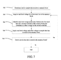
- FIG. 7 is a flow chart of one implementation of a method for sampling data of a memory block.
- a controller of a non-volatile memory system determines a need to sample data stored at a first group of memory cells, such as a set of single level memory cells of a first memory block.
- the controller may determines to sample the data prior to transferring the data to a second set of memory cells, such as a group of triple level memory cells of a second memory block.
- a read level voltage acquisition module determines a read level voltage for a first word line of the memory block.
- the read level voltage acquisition module determines the read level of voltages by applying a number of voltages to the word line and determining the voltage level that results in the fewest number of errors.
- the read level voltage acquisition module defines the read level to be the determined voltage level that resulted in the fewest number of errors. Examples of techniques for determining a read level voltage can be found in U.S. Pat. No. 8,713,380, assigned to SanDisk Technologies, Inc.
- the read level voltage acquisition module both determines that a second word line of the memory block is associated with the first word line of the memory block and determines an offset voltage for the second word line of the memory block. In some implementations, to determine that the second word line is associated with the first word line and to determine the offset voltage, the read level acquisition module accesses one or more lookup tables such as one or more offset voltage tables stored at the non-volatile memory system.
- the read level voltage acquisition module may further utilize one or more factors such as a life stage of the memory block, a program/erase count of the memory block, a program/disturb count of the memory block, a read/disturb count of the memory block, and/or a level of data retention of the memory block to determine the offset voltage.
- the read level voltage acquisition module may utilize two tables to determine for a second word line of a memory block whose P/E count indicates that the memory block is at mid-life stage, and whose read/disturb count is between 5,000 and 10,000, that the offset voltage is 3 digital-analog conversion (“DAC”).
- 1 DAC represents 100 mV.
- the read level voltage acquisition module initially accesses a table to determine which word line the second word line is related to.
- Table 1 illustrates that the second word line of the memory block is associated with the first word line of the memory block.
- the read level voltage acquisition module then accesses another table to determine offset voltage for the second word line. Because the memory block is at mid-life stage and the read/disturb count for the memory block is between 5,000 and 10,000, the offset voltage is 3 DAC from the acquired read level voltage of the first word line.
- the controller and/or the read level voltage acquisition module may generate one or more offset voltage lookup tables based on an analysis of empirical data observed at the non-volatile memory system or based on an analysis of empirical data from other similar non-volatile memory system.
- the controller and/or the read level voltage acquisition module may generate the offset voltage lookup table by periodically acquiring relationships between the different word lines of the memory block. The generation of one or more offset voltage lookup tables is described in more detail below in conjunction with FIGS. 8 and 9 .
- the controller and/or the read level voltage acquisition module applies the read level voltage acquired at step 704 and the offset voltage acquired at step 706 to the second word line to sample data of the memory block.
- the controller and/or the read level acquisition module determines whether one or more errors exist in the sampled data of the memory block.
- the controller determines that one or more errors exist in the sampled data, the controller repeats the above-described process beginning at step 704 with the read level voltage acquisition module determining a read level voltage for a first word line of the memory block.
- the above-described method may be implemented for multiple word lines during the sampling of a memory block.
- the read level acquisition module may also determine an offset voltage for third, fourth, etc. word lines for use in sampling data of the memory block.
- FIG. 8 is a flow chart of one method for updating one or more offset voltage lookup tables that include read level voltage relationships between word lines of a memory block.
- a read level voltage acquisition module of a controller of a non-volatile memory system determines a need to generate an updated offset voltage lookup table during operation of the non-volatile memory system.
- the read level voltage acquisition module may determine a need to generate the offset voltage lookup table after a number of errors within sampled data exceeds a threshold; periodically after a defined number of program, erase, read, and/or disturb operations occurs at the non-volatile memory system; based on a time of a write to increase date retention; and/or any other reason that may indicate that the voltage offsets within the offset voltage lookup table may no longer be valid.
- the controller samples data read from word lines of the memory block, and at step 806 , the controller determines whether a number of errors within the sampled data exceeds a threshold.
- the threshold may be set at 30 bits in error within an ECC doe word. However, it will be appreciated that other thresholds may be used.
- the controller determines at step 808 that the one or more offset lookup tables are valid and does not generate updated tables.
- the controller acquires the read level voltages for the word lines of the memory block at step 810 . Based on the acquired read level voltages, at step 812 , the controller generates one or more updated offset voltage lookup tables. Updating the offset voltage lookup tables may include both changing an amount of offset voltage added to an acquired read level voltage and changing which word lines are related to each other within the offset voltage lookup table.
- offset voltage lookup tables may show that word line 0 is related to word line 1 such that an offset of 1 DAC should be applied to word line 1 in addition to a read level acquired at word line 0. Additionally, prior to an update, the offset voltage lookup tables may show that word line 0 is also related to word line 4 such that an offset of 2 DAC should be applied to word line 4 in addition to a read level acquired at word line 0.
- the offset voltage lookup tables may show that word line 0 is still related to word line 1. However, rather than an offset of 1 DAC, the offset voltage lookup table shows that 2 DAC should be applied to word line 1 in addition to a read level acquired at word line 0.
- the offset voltage lookup tables may show that word line 0 is no longer related to word line 4. Instead, the offset voltage lookup table may show that word line 4 is not related to any other word line or the offset voltage lookup table may show that word line 4 is related to a new word line. For example, the offset voltage lookup table may show that word line 2 is related to word line 4 such that an offset of 2 DAC should be applied to word line 4 in addition to a read level acquired at word line 2.
- FIG. 9 is a flow chart of another method for generating one or more offset voltage lookup tables that include read level voltage relationships between word lines of a memory block.
- a read level voltage acquisition module of a controller of a non-volatile memory system determines a need to generate an updated offset voltage lookup table during operation of the non-volatile memory system.
- the read level voltage acquisition module may determine a need to generate the offset voltage lookup table after a number of errors within sampled data exceeds a threshold; periodically after a defined number of program, erase, read, and/or disturb operations occurs at the non-volatile memory system; after a set period of time in order to improve data retention; and/or any other reason that may indicate that the voltage offsets within the offset voltage lookup table may no longer be valid.
- the read level voltage acquisition module determines read level voltage relationships between the word lines of a memory block based on empirical data.
- the read level acquisition module analyzes empirical data collected at similar non-volatile memory systems and stored at the non-volatile memory system to determine the read level voltages relationships. By analyzing the empirical data, the read level voltage acquisition unit is able to determine historically, which word lines have the same read level voltages and/or which word lines have read level voltages that are offset by defined amounts, such as +1 DAC or +2 DAC.
- the read level voltage acquisition module may test the read level voltages that were determined based on the empirical data to examine if any errors are within the sampled data. When errors are detected, the read level voltage acquisition module may acquire a read level voltage of one or more word lines where errors were present in the sampled data in order to dynamically adjust the read level voltages based on actual performance of the memory block.
- the read level voltage acquisition module generates and/or updates an offset voltage lookup table based on the relationships between the word lines of the memory block determined at step 904 .
- FIGS. 1-9 illustrate systems and methods for sampling data at a non-volatile memory system.
- non-volatile memory systems may utilize one or more offset voltage lookup tables that allow a controller and a read level voltage acquisition module of the controller to efficiently verify data at a first memory block of the non-volatile memory system before transferring the data to a second memory block of the non-volatile memory system.
- the controller and the read level voltage acquisition module sample data stored at a memory block based on relationships between word lines of the memory blocks and characteristics of the non-volatile memory system such as a life stage of the memory block, a program/erase count of the memory block, a program/disturb count of the memory block, a read/disturb count of the memory block, and/or a level of data retention of the memory block. Further, during operation of the non-volatile memory system, the read level acquisition module is able to dynamically update the relationships between the word lines of a memory block.
- semiconductor memory devices such as those described in the present application may include volatile memory devices, such as dynamic random access memory (“DRAM”) or static random access memory (“SRAM”) devices, non-volatile memory devices, such as resistive random access memory (“ReRAM”), electrically erasable programmable read only memory (“EEPROM”), flash memory (which can also be considered a subset of EEPROM), ferroelectric random access memory (“FRAM”), and magnetoresistive random access memory (“MRAM”), and other semiconductor elements capable of storing information.
- volatile memory devices such as dynamic random access memory (“DRAM”) or static random access memory (“SRAM”) devices
- non-volatile memory devices such as resistive random access memory (“ReRAM”), electrically erasable programmable read only memory (“EEPROM”), flash memory (which can also be considered a subset of EEPROM), ferroelectric random access memory (“FRAM”), and magnetoresistive random access memory (“MRAM”), and other semiconductor elements capable of storing information.
- ReRAM resistive random access memory
- EEPROM
- the memory devices can be formed from passive and/or active elements, in any combinations.
- passive semiconductor memory elements include ReRAM device elements, which in some embodiments include a resistivity switching storage element, such as an anti-fuse, phase change material, etc., and optionally a steering element, such as a diode, etc.
- active semiconductor memory elements include EEPROM and flash memory device elements, which in some embodiments include elements containing a charge storage region, such as a floating gate, conductive nanoparticles, or a charge storage dielectric material.
- Multiple memory elements may be configured so that they are connected in series or so that each element is individually accessible.
- flash memory devices in a NAND configuration typically contain memory elements connected in series.
- a NAND memory array may be configured so that the array is composed of multiple strings of memory in which a string is composed of multiple memory elements sharing a single bit line and accessed as a group.
- memory elements may be configured so that each element is individually accessible, e.g., a NOR memory array.
- NAND and NOR memory configurations are exemplary, and memory elements may be otherwise configured.
- the semiconductor memory elements located within and/or over a substrate may be arranged in two or three dimensions, such as a two dimensional memory structure or a three dimensional memory structure.
- the semiconductor memory elements are arranged in a single plane or a single memory device level.
- memory elements are arranged in a plane (e.g., in an x-z direction plane) which extends substantially parallel to a major surface of a substrate that supports the memory elements.
- the substrate may be a wafer over or in which the layer of the memory elements are formed or it may be a carrier substrate which is attached to the memory elements after they are formed.
- the substrate may include a semiconductor such as silicon.
- the memory elements may be arranged in the single memory device level in an ordered array, such as in a plurality of rows and/or columns. However, the memory elements may be arrayed in non-regular or non-orthogonal configurations.
- the memory elements may each have two or more electrodes or contact lines, such as bit lines and word lines.
- a three dimensional memory array is arranged so that memory elements occupy multiple planes or multiple memory device levels, thereby forming a structure in three dimensions (i.e., in the x, y and z directions, where the y direction is substantially perpendicular and the x and z directions are substantially parallel to the major surface of the substrate).
- a three dimensional memory structure may be vertically arranged as a stack of multiple two dimensional memory device levels.
- a three dimensional memory array may be arranged as multiple vertical columns (e.g., columns extending substantially perpendicular to the major surface of the substrate, i.e., in the y direction) with each column having multiple memory elements in each column.
- the columns may be arranged in a two dimensional configuration, e.g., in an x-z plane, resulting in a three dimensional arrangement of memory elements with elements on multiple vertically stacked memory planes.
- Other configurations of memory elements in three dimensions can also constitute a three dimensional memory array.
- the memory elements may be coupled together to form a NAND string within a single horizontal (e.g., x-z) memory device levels.
- the memory elements may be coupled together to form a vertical NAND string that traverses across multiple horizontal memory device levels.
- Other three dimensional configurations can be envisioned wherein some NAND strings contain memory elements in a single memory level while other strings contain memory elements which span through multiple memory levels.
- Three dimensional memory arrays may also be designed in a NOR configuration and in a ReRAM configuration.
- a monolithic three dimensional memory array typically, one or more memory device levels are formed above a single substrate.
- the monolithic three dimensional memory array may also have one or more memory layers at least partially within the single substrate.
- the substrate may include a semiconductor such as silicon.
- the layers constituting each memory device level of the array are typically formed on the layers of the underlying memory device levels of the array.
- layers of adjacent memory device levels of a monolithic three dimensional memory array may be shared or have intervening layers between memory device levels.
- non-monolithic stacked memories can be constructed by forming memory levels on separate substrates and then stacking the memory levels atop each other. The substrates may be thinned or removed from the memory device levels before stacking, but as the memory device levels are initially formed over separate substrates, the resulting memory arrays are not monolithic three dimensional memory arrays. Further, multiple two dimensional memory arrays or three dimensional memory arrays (monolithic or non-monolithic) may be formed on separate chips and then packaged together to form a stacked-chip memory device.
- Associated circuitry is typically required for operation of the memory elements and for communication with the memory elements.
- memory devices may have circuitry used for controlling and driving memory elements to accomplish functions such as programming and reading.
- This associated circuitry may be on the same substrate as the memory elements and/or on a separate substrate.
- a controller for memory read-write operations may be located on a separate controller chip and/or on the same substrate as the memory elements.
Landscapes
- Engineering & Computer Science (AREA)
- Theoretical Computer Science (AREA)
- Human Computer Interaction (AREA)
- Physics & Mathematics (AREA)
- General Engineering & Computer Science (AREA)
- General Physics & Mathematics (AREA)
- Computer Security & Cryptography (AREA)
- Read Only Memory (AREA)
- Techniques For Improving Reliability Of Storages (AREA)
Abstract
Description
| TABLE 1 |
| Example Word Line Association Table |
| Word Line | Associated Word Line | ||
| Word line 0 | Acquired Read Level Voltage | ||
| Word line 1 | Acquired Read Level Voltage | ||
| Word line 2 | Word line 1 | ||
| Word line 3 | Acquired Read Level Voltage | ||
| Word line 4 | Word line 0 | ||
| Word line 5 | Word line 3 | ||
| Word line 6 | Word line 3 | ||
| . . . | . . . | ||
| Word line n | Acquired Read Level Voltage | ||
| TABLE 2 |
| Example Offset Voltage Lookup Table for Second Word Line |
| R/D Count | R/D Count | ||
| 0-5,000 | 5,000-10,000 | ||
| P/E Count | Acquired Read Level | Acquired Read Level |
| Beginning of Life | Voltage + 1 DAC | Voltage + 2 DAC |
| P/E Count | Acquired Read Level | Acquired Read Level |
| Middle of Life | Voltage + 2 DAC | Voltage + 3 DAC |
| P/E Count | Acquired Read Level | Acquired Read Level |
| End of Life | Voltage + 3 DAC | Voltage + 4 DAC |
Claims (20)
Priority Applications (1)
| Application Number | Priority Date | Filing Date | Title |
|---|---|---|---|
| US14/918,050 US9785357B2 (en) | 2015-10-20 | 2015-10-20 | Systems and methods for sampling data at a non-volatile memory system |
Applications Claiming Priority (1)
| Application Number | Priority Date | Filing Date | Title |
|---|---|---|---|
| US14/918,050 US9785357B2 (en) | 2015-10-20 | 2015-10-20 | Systems and methods for sampling data at a non-volatile memory system |
Publications (2)
| Publication Number | Publication Date |
|---|---|
| US20170109040A1 US20170109040A1 (en) | 2017-04-20 |
| US9785357B2 true US9785357B2 (en) | 2017-10-10 |
Family
ID=58523769
Family Applications (1)
| Application Number | Title | Priority Date | Filing Date |
|---|---|---|---|
| US14/918,050 Active 2035-11-11 US9785357B2 (en) | 2015-10-20 | 2015-10-20 | Systems and methods for sampling data at a non-volatile memory system |
Country Status (1)
| Country | Link |
|---|---|
| US (1) | US9785357B2 (en) |
Cited By (27)
| Publication number | Priority date | Publication date | Assignee | Title |
|---|---|---|---|---|
| US20200058359A1 (en) * | 2018-08-14 | 2020-02-20 | Samsung Electronics Co., Ltd. | Storage device including nonvolatile memory device and operating method thereof |
| US11275681B1 (en) | 2017-11-17 | 2022-03-15 | Pure Storage, Inc. | Segmented write requests |
| US11416338B2 (en) | 2020-04-24 | 2022-08-16 | Pure Storage, Inc. | Resiliency scheme to enhance storage performance |
| US11474986B2 (en) | 2020-04-24 | 2022-10-18 | Pure Storage, Inc. | Utilizing machine learning to streamline telemetry processing of storage media |
| US11487455B2 (en) | 2020-12-17 | 2022-11-01 | Pure Storage, Inc. | Dynamic block allocation to optimize storage system performance |
| US11500570B2 (en) | 2018-09-06 | 2022-11-15 | Pure Storage, Inc. | Efficient relocation of data utilizing different programming modes |
| US11507297B2 (en) | 2020-04-15 | 2022-11-22 | Pure Storage, Inc. | Efficient management of optimal read levels for flash storage systems |
| US11513974B2 (en) | 2020-09-08 | 2022-11-29 | Pure Storage, Inc. | Using nonce to control erasure of data blocks of a multi-controller storage system |
| US11520514B2 (en) | 2018-09-06 | 2022-12-06 | Pure Storage, Inc. | Optimized relocation of data based on data characteristics |
| US11581943B2 (en) | 2016-10-04 | 2023-02-14 | Pure Storage, Inc. | Queues reserved for direct access via a user application |
| US11614893B2 (en) | 2010-09-15 | 2023-03-28 | Pure Storage, Inc. | Optimizing storage device access based on latency |
| US20230098775A1 (en) * | 2021-09-30 | 2023-03-30 | Innogrit Technologies Co., Ltd. | Selecting read reference voltage using historical decoding information |
| US11630593B2 (en) | 2021-03-12 | 2023-04-18 | Pure Storage, Inc. | Inline flash memory qualification in a storage system |
| US11681448B2 (en) | 2020-09-08 | 2023-06-20 | Pure Storage, Inc. | Multiple device IDs in a multi-fabric module storage system |
| US11714572B2 (en) | 2019-06-19 | 2023-08-01 | Pure Storage, Inc. | Optimized data resiliency in a modular storage system |
| US11768763B2 (en) | 2020-07-08 | 2023-09-26 | Pure Storage, Inc. | Flash secure erase |
| US11832410B2 (en) | 2021-09-14 | 2023-11-28 | Pure Storage, Inc. | Mechanical energy absorbing bracket apparatus |
| US11947814B2 (en) | 2017-06-11 | 2024-04-02 | Pure Storage, Inc. | Optimizing resiliency group formation stability |
| US11994723B2 (en) | 2021-12-30 | 2024-05-28 | Pure Storage, Inc. | Ribbon cable alignment apparatus |
| US12001684B2 (en) | 2019-12-12 | 2024-06-04 | Pure Storage, Inc. | Optimizing dynamic power loss protection adjustment in a storage system |
| US12001688B2 (en) | 2019-04-29 | 2024-06-04 | Pure Storage, Inc. | Utilizing data views to optimize secure data access in a storage system |
| US12008266B2 (en) | 2010-09-15 | 2024-06-11 | Pure Storage, Inc. | Efficient read by reconstruction |
| US12032848B2 (en) | 2021-06-21 | 2024-07-09 | Pure Storage, Inc. | Intelligent block allocation in a heterogeneous storage system |
| US12039165B2 (en) | 2016-10-04 | 2024-07-16 | Pure Storage, Inc. | Utilizing allocation shares to improve parallelism in a zoned drive storage system |
| US12099742B2 (en) | 2021-03-15 | 2024-09-24 | Pure Storage, Inc. | Utilizing programming page size granularity to optimize data segment storage in a storage system |
| US12153818B2 (en) | 2020-09-24 | 2024-11-26 | Pure Storage, Inc. | Bucket versioning snapshots |
| US12175124B2 (en) | 2018-04-25 | 2024-12-24 | Pure Storage, Inc. | Enhanced data access using composite data views |
Families Citing this family (20)
| Publication number | Priority date | Publication date | Assignee | Title |
|---|---|---|---|---|
| KR102695928B1 (en) * | 2016-12-19 | 2024-08-16 | 삼성전자주식회사 | Read operation method of nonvoltile memory, memory system including the same and operation method thereof |
| US11069418B1 (en) * | 2016-12-30 | 2021-07-20 | EMC IP Holding Company LLC | Method and system for offline program/erase count estimation |
| US10289550B1 (en) | 2016-12-30 | 2019-05-14 | EMC IP Holding Company LLC | Method and system for dynamic write-back cache sizing in solid state memory storage |
| US10338983B2 (en) | 2016-12-30 | 2019-07-02 | EMC IP Holding Company LLC | Method and system for online program/erase count estimation |
| US10290331B1 (en) | 2017-04-28 | 2019-05-14 | EMC IP Holding Company LLC | Method and system for modulating read operations to support error correction in solid state memory |
| US10403366B1 (en) | 2017-04-28 | 2019-09-03 | EMC IP Holding Company LLC | Method and system for adapting solid state memory write parameters to satisfy performance goals based on degree of read errors |
| US10290347B2 (en) | 2017-06-30 | 2019-05-14 | Western Digital Technologies, Inc. | Compacting operating parameter groups in solid state memory devices |
| US10289341B2 (en) * | 2017-06-30 | 2019-05-14 | Western Digital Technologies, Inc. | Operating parameter offsets in solid state memory devices |
| US10446254B1 (en) * | 2018-05-03 | 2019-10-15 | Western Digital Technologies, Inc. | Method for maximizing power efficiency in memory interface block |
| CN111863114B (en) * | 2019-04-29 | 2022-05-03 | 长鑫存储技术有限公司 | Chip sampling quasi-position determining method and device |
| KR102711406B1 (en) * | 2019-05-29 | 2024-09-30 | 에스케이하이닉스 주식회사 | Memory device, memory controller and storage system having the same |
| US11335418B2 (en) * | 2019-12-30 | 2022-05-17 | Micron Technology, Inc. | Memory device including dynamic programming voltage |
| US11250904B1 (en) * | 2020-09-30 | 2022-02-15 | Piecemakers Technology, Inc. | DRAM with inter-section, page-data-copy scheme for low power and wide data access |
| US12537049B2 (en) | 2020-09-30 | 2026-01-27 | Piecemakers Technology, Inc. | Apparatus for page-copy data accessing |
| US11636897B2 (en) | 2021-03-03 | 2023-04-25 | Sandisk Technologies Llc | Peak current and program time optimization through loop dependent voltage ramp target and timing control |
| US12314598B2 (en) * | 2021-03-03 | 2025-05-27 | Gylicon Ltd | Solid state storage device with look-up tables providing improved reference voltages |
| WO2023146520A1 (en) * | 2022-01-27 | 2023-08-03 | Siemens Industry Software Inc. | Memory built-in self-test with address skipping trim search |
| US11894080B2 (en) | 2022-04-29 | 2024-02-06 | Sandisk Technologies Llc | Time-tagging read levels of multiple wordlines for open block data retention |
| US12039202B2 (en) * | 2022-09-16 | 2024-07-16 | Western Digital Technologies, Inc. | Dynamic ordering of memory die programming in a metablock |
| CN118800307A (en) * | 2023-04-14 | 2024-10-18 | 慧荣科技股份有限公司 | Data storage device and method for searching read voltage thereof |
Citations (1)
| Publication number | Priority date | Publication date | Assignee | Title |
|---|---|---|---|---|
| US20160148702A1 (en) * | 2014-11-20 | 2016-05-26 | HGST Netherlands B.V. | Calibrating optimal read levels |
-
2015
- 2015-10-20 US US14/918,050 patent/US9785357B2/en active Active
Patent Citations (1)
| Publication number | Priority date | Publication date | Assignee | Title |
|---|---|---|---|---|
| US20160148702A1 (en) * | 2014-11-20 | 2016-05-26 | HGST Netherlands B.V. | Calibrating optimal read levels |
Cited By (35)
| Publication number | Priority date | Publication date | Assignee | Title |
|---|---|---|---|---|
| US12282686B2 (en) | 2010-09-15 | 2025-04-22 | Pure Storage, Inc. | Performing low latency operations using a distinct set of resources |
| US11614893B2 (en) | 2010-09-15 | 2023-03-28 | Pure Storage, Inc. | Optimizing storage device access based on latency |
| US12008266B2 (en) | 2010-09-15 | 2024-06-11 | Pure Storage, Inc. | Efficient read by reconstruction |
| US11581943B2 (en) | 2016-10-04 | 2023-02-14 | Pure Storage, Inc. | Queues reserved for direct access via a user application |
| US12039165B2 (en) | 2016-10-04 | 2024-07-16 | Pure Storage, Inc. | Utilizing allocation shares to improve parallelism in a zoned drive storage system |
| US11947814B2 (en) | 2017-06-11 | 2024-04-02 | Pure Storage, Inc. | Optimizing resiliency group formation stability |
| US11275681B1 (en) | 2017-11-17 | 2022-03-15 | Pure Storage, Inc. | Segmented write requests |
| US12175124B2 (en) | 2018-04-25 | 2024-12-24 | Pure Storage, Inc. | Enhanced data access using composite data views |
| CN110827907B (en) * | 2018-08-14 | 2025-05-09 | 三星电子株式会社 | Storage device including non-volatile memory device and operation method thereof |
| US11004517B2 (en) * | 2018-08-14 | 2021-05-11 | Samsung Electronics Co., Ltd. | Storage device including nonvolatile memory device and operating method thereof |
| KR20200019385A (en) * | 2018-08-14 | 2020-02-24 | 삼성전자주식회사 | Storage device including nonvolatile memory device and operating method thereof |
| US20200058359A1 (en) * | 2018-08-14 | 2020-02-20 | Samsung Electronics Co., Ltd. | Storage device including nonvolatile memory device and operating method thereof |
| CN110827907A (en) * | 2018-08-14 | 2020-02-21 | 三星电子株式会社 | Storage device including nonvolatile memory device and method of operating the same |
| US11500570B2 (en) | 2018-09-06 | 2022-11-15 | Pure Storage, Inc. | Efficient relocation of data utilizing different programming modes |
| US11520514B2 (en) | 2018-09-06 | 2022-12-06 | Pure Storage, Inc. | Optimized relocation of data based on data characteristics |
| US12001688B2 (en) | 2019-04-29 | 2024-06-04 | Pure Storage, Inc. | Utilizing data views to optimize secure data access in a storage system |
| US11714572B2 (en) | 2019-06-19 | 2023-08-01 | Pure Storage, Inc. | Optimized data resiliency in a modular storage system |
| US12001684B2 (en) | 2019-12-12 | 2024-06-04 | Pure Storage, Inc. | Optimizing dynamic power loss protection adjustment in a storage system |
| US11507297B2 (en) | 2020-04-15 | 2022-11-22 | Pure Storage, Inc. | Efficient management of optimal read levels for flash storage systems |
| US11416338B2 (en) | 2020-04-24 | 2022-08-16 | Pure Storage, Inc. | Resiliency scheme to enhance storage performance |
| US11474986B2 (en) | 2020-04-24 | 2022-10-18 | Pure Storage, Inc. | Utilizing machine learning to streamline telemetry processing of storage media |
| US11768763B2 (en) | 2020-07-08 | 2023-09-26 | Pure Storage, Inc. | Flash secure erase |
| US11513974B2 (en) | 2020-09-08 | 2022-11-29 | Pure Storage, Inc. | Using nonce to control erasure of data blocks of a multi-controller storage system |
| US11681448B2 (en) | 2020-09-08 | 2023-06-20 | Pure Storage, Inc. | Multiple device IDs in a multi-fabric module storage system |
| US12153818B2 (en) | 2020-09-24 | 2024-11-26 | Pure Storage, Inc. | Bucket versioning snapshots |
| US11487455B2 (en) | 2020-12-17 | 2022-11-01 | Pure Storage, Inc. | Dynamic block allocation to optimize storage system performance |
| US11630593B2 (en) | 2021-03-12 | 2023-04-18 | Pure Storage, Inc. | Inline flash memory qualification in a storage system |
| US12099742B2 (en) | 2021-03-15 | 2024-09-24 | Pure Storage, Inc. | Utilizing programming page size granularity to optimize data segment storage in a storage system |
| US12032848B2 (en) | 2021-06-21 | 2024-07-09 | Pure Storage, Inc. | Intelligent block allocation in a heterogeneous storage system |
| US11832410B2 (en) | 2021-09-14 | 2023-11-28 | Pure Storage, Inc. | Mechanical energy absorbing bracket apparatus |
| US20230098775A1 (en) * | 2021-09-30 | 2023-03-30 | Innogrit Technologies Co., Ltd. | Selecting read reference voltage using historical decoding information |
| US11735286B2 (en) * | 2021-09-30 | 2023-08-22 | Innogrit Technologies Co., Ltd. | Selecting read reference voltage using historical decoding information |
| US20230360715A1 (en) * | 2021-09-30 | 2023-11-09 | Innogrit Technologies Co., Ltd. | Selecting read reference voltage using historical decoding information |
| US12431210B2 (en) * | 2021-09-30 | 2025-09-30 | Innogrit Technologies Co., Ltd. | Selecting read reference voltage using historical decoding information |
| US11994723B2 (en) | 2021-12-30 | 2024-05-28 | Pure Storage, Inc. | Ribbon cable alignment apparatus |
Also Published As
| Publication number | Publication date |
|---|---|
| US20170109040A1 (en) | 2017-04-20 |
Similar Documents
| Publication | Publication Date | Title |
|---|---|---|
| US9785357B2 (en) | Systems and methods for sampling data at a non-volatile memory system | |
| US10929285B2 (en) | Storage system and method for generating a reverse map during a background operation and storing it in a host memory buffer | |
| US10157004B2 (en) | Storage system and method for recovering data corrupted in a host memory buffer | |
| US10102920B2 (en) | Memory system with a weighted read retry table | |
| US9530517B2 (en) | Read disturb detection in open blocks | |
| US9886341B2 (en) | Optimizing reclaimed flash memory | |
| US10282251B2 (en) | System and method for protecting firmware integrity in a multi-processor non-volatile memory system | |
| US10468117B2 (en) | Read threshold adjustment with feedback information from error recovery | |
| US20170287568A1 (en) | System and Method for Erase Detection before Programming of a Storage Device | |
| US11036407B1 (en) | Storage system and method for smart folding | |
| US9728262B2 (en) | Non-volatile memory systems with multi-write direction memory units | |
| US9582435B2 (en) | Memory system and method for efficient padding of memory pages | |
| US9812209B2 (en) | System and method for memory integrated circuit chip write abort indication | |
| US11442666B2 (en) | Storage system and dual-write programming method with reverse order for secondary block | |
| US11437104B2 (en) | Storage system and method for a hybrid quad-level cell (QLC) write scheme for reduced random access memory (RAM) footprint | |
| US20180074891A1 (en) | Storage System and Method for Reducing XOR Recovery Time | |
| US11231997B2 (en) | Storage system and method for balanced quad-level cell (QLC) coding with margin for an internal data load (IDL) read | |
| US10096355B2 (en) | Dynamic management of programming states to improve endurance | |
| US9620201B1 (en) | Storage system and method for using hybrid blocks with sub-block erase operations | |
| US11334256B2 (en) | Storage system and method for boundary wordline data retention handling | |
| US9678684B2 (en) | Systems and methods for performing an adaptive sustain write in a memory system | |
| US9548105B1 (en) | Enhanced post-write read for 3-D memory | |
| US12271261B2 (en) | Data storage device and method for host-assisted improved error recovery using a correlation factor | |
| US11915772B1 (en) | Data storage device and method for power on reset and read error handling | |
| US11809331B1 (en) | Storage system and method for avoiding header to improve parity |
Legal Events
| Date | Code | Title | Description |
|---|---|---|---|
| AS | Assignment |
Owner name: SANDISK TECHNOLOGIES INC., TEXAS Free format text: ASSIGNMENT OF ASSIGNORS INTEREST;ASSIGNORS:RAGHU, DEEPAK;AVILA, CHRIS;LIANG, GUIRONG;AND OTHERS;SIGNING DATES FROM 20151005 TO 20151016;REEL/FRAME:036842/0992 |
|
| AS | Assignment |
Owner name: SANDISK TECHNOLOGIES LLC, TEXAS Free format text: CHANGE OF NAME;ASSIGNOR:SANDISK TECHNOLOGIES INC;REEL/FRAME:038812/0954 Effective date: 20160516 |
|
| STCF | Information on status: patent grant |
Free format text: PATENTED CASE |
|
| MAFP | Maintenance fee payment |
Free format text: PAYMENT OF MAINTENANCE FEE, 4TH YEAR, LARGE ENTITY (ORIGINAL EVENT CODE: M1551); ENTITY STATUS OF PATENT OWNER: LARGE ENTITY Year of fee payment: 4 |
|
| AS | Assignment |
Owner name: SANDISK TECHNOLOGIES, INC., CALIFORNIA Free format text: ASSIGNMENT OF ASSIGNORS INTEREST;ASSIGNOR:SANDISK TECHNOLOGIES LLC;REEL/FRAME:069796/0423 Effective date: 20241227 |
|
| MAFP | Maintenance fee payment |
Free format text: PAYMENT OF MAINTENANCE FEE, 8TH YEAR, LARGE ENTITY (ORIGINAL EVENT CODE: M1552); ENTITY STATUS OF PATENT OWNER: LARGE ENTITY Year of fee payment: 8 |
|
| AS | Assignment |
Owner name: SANDISK TECHNOLOGIES, INC., CALIFORNIA Free format text: PARTIAL RELEASE OF SECURITY INTERESTS;ASSIGNOR:JPMORGAN CHASE BANK, N.A., AS AGENT;REEL/FRAME:071382/0001 Effective date: 20250424 Owner name: JPMORGAN CHASE BANK, N.A., AS COLLATERAL AGENT, ILLINOIS Free format text: SECURITY AGREEMENT;ASSIGNOR:SANDISK TECHNOLOGIES, INC.;REEL/FRAME:071050/0001 Effective date: 20250424 |