US9780807B2 - Data processing apparatus, data processing method, and non-transitory computer readable medium - Google Patents
Data processing apparatus, data processing method, and non-transitory computer readable medium Download PDFInfo
- Publication number
- US9780807B2 US9780807B2 US15/251,691 US201615251691A US9780807B2 US 9780807 B2 US9780807 B2 US 9780807B2 US 201615251691 A US201615251691 A US 201615251691A US 9780807 B2 US9780807 B2 US 9780807B2
- Authority
- US
- United States
- Prior art keywords
- data
- line
- circuit
- decoding result
- reconfiguration
- Prior art date
- Legal status (The legal status is an assumption and is not a legal conclusion. Google has not performed a legal analysis and makes no representation as to the accuracy of the status listed.)
- Expired - Fee Related
Links
Images


Classifications
-
- H—ELECTRICITY
- H03—ELECTRONIC CIRCUITRY
- H03M—CODING; DECODING; CODE CONVERSION IN GENERAL
- H03M7/00—Conversion of a code where information is represented by a given sequence or number of digits to a code where the same, similar or subset of information is represented by a different sequence or number of digits
- H03M7/30—Compression; Expansion; Suppression of unnecessary data, e.g. redundancy reduction
- H03M7/46—Conversion to or from run-length codes, i.e. by representing the number of consecutive digits, or groups of digits, of the same kind by a code word and a digit indicative of that kind
-
- H—ELECTRICITY
- H03—ELECTRONIC CIRCUITRY
- H03M—CODING; DECODING; CODE CONVERSION IN GENERAL
- H03M7/00—Conversion of a code where information is represented by a given sequence or number of digits to a code where the same, similar or subset of information is represented by a different sequence or number of digits
- H03M7/30—Compression; Expansion; Suppression of unnecessary data, e.g. redundancy reduction
- H03M7/40—Conversion to or from variable length codes, e.g. Shannon-Fano code, Huffman code, Morse code
-
- H—ELECTRICITY
- H03—ELECTRONIC CIRCUITRY
- H03M—CODING; DECODING; CODE CONVERSION IN GENERAL
- H03M7/00—Conversion of a code where information is represented by a given sequence or number of digits to a code where the same, similar or subset of information is represented by a different sequence or number of digits
- H03M7/30—Compression; Expansion; Suppression of unnecessary data, e.g. redundancy reduction
- H03M7/60—General implementation details not specific to a particular type of compression
- H03M7/6005—Decoder aspects
-
- H—ELECTRICITY
- H03—ELECTRONIC CIRCUITRY
- H03M—CODING; DECODING; CODE CONVERSION IN GENERAL
- H03M7/00—Conversion of a code where information is represented by a given sequence or number of digits to a code where the same, similar or subset of information is represented by a different sequence or number of digits
- H03M7/30—Compression; Expansion; Suppression of unnecessary data, e.g. redundancy reduction
- H03M7/60—General implementation details not specific to a particular type of compression
- H03M7/6064—Selection of Compressor
Definitions
- the present invention relates to a data processing apparatus, a data processing method, and a non-transitory computer readable medium.
- a data processing apparatus including a circuit selecting unit and a decoding processor.
- the circuit selecting unit selects a decoder circuit for each data part of encoded target data.
- the decoder circuit is suitable for an arrangement of run lengths in the data part.
- the decoding processor performs reconfiguration to form the decoder circuit selected for the data part, and decodes the target data.
- FIG. 1 is a diagram illustrating an exemplary data processing apparatus desirable for an exemplary embodiment of the present invention
- FIG. 2 is a diagram illustrating exemplary encoding and decoding of target data
- FIG. 3 is a diagram illustrating a data processor of a first example
- FIG. 4 is a diagram illustrating exemplary processing performed by a preprocessor and a decoding processor
- FIG. 5 is a diagram illustrating circuit data of the first example which is stored in a circuit data memory
- FIG. 6 is a diagram illustrating a data processor of a second example
- FIG. 7 is a diagram illustrating exemplary processing performed by a target data analyzing unit and a decoding processor
- FIG. 8 is a diagram illustrating circuit data of the second example which is stored in the circuit data memory
- FIG. 9 is a diagram illustrating exemplary circuit selection performed by a circuit selecting unit
- FIG. 10 is a flowchart of a process of the second example which is performed by the data processor
- FIG. 11 is a diagram illustrating a data processor of a third example.
- FIG. 12 is a flowchart of a process of the third example which is performed by the data processor.
- FIG. 1 is a diagram illustrating an exemplary data processing apparatus 100 that is desirable for an exemplary embodiment for carrying out the present invention.
- the data processing apparatus 100 in FIG. 1 includes a data processor 10 which performs data processing on target data (data to be processed).
- a desirable example of the target data which is to be processed by the data processing apparatus 100 in FIG. 1 is image data (including data containing only characters, numbers, and symbols) or the like.
- image data is transmitted from an external apparatus such as a computer to the data processing apparatus 100 .
- the data processing apparatus 100 in FIG. 1 may be integrated into an image processing apparatus provided with an image reading function (scan function) and the like, and image data obtained from a medium such as paper by using the image reading function may be used as the target data. Further, an image corresponding to image data obtained after processing performed by the data processing apparatus 100 may be printed on paper or the like, or image data obtained after the processing may be supplied to an external apparatus. Desirable examples of the image processing apparatus include a copier, a printer, and a facsimile (fax). Further, a multi-function device provided with multiple functions that are among a copier function, a printer function, and a facsimile function is also a desirable example of the image processing apparatus.
- the data processor 10 performs data processing on the target data.
- the data processor 10 includes a decoding processor, a circuit selecting unit, and a reconfiguration controller.
- the target data which has been encoded is decoded, and the decoded data is obtained.
- the circuit configuration of the decoding processor is implemented by using a programmable and reconfigurable circuit.
- the circuit selecting unit selects a decoder circuit that is to be formed through reconfiguration in the decoding processor.
- the reconfiguration controller controls reconfiguration of the decoding processor (reconfigurable circuit) so that the decoder circuit selected by the circuit selecting unit is formed through the reconfiguration.
- a reconfigurable circuit is a circuit for which the internal circuit configuration is reconfigurable (programmable).
- a dynamic reconfigurable processor DSP
- DSP dynamic reconfigurable processor
- another device for example, a programmable logic circuit, such as a programmable logic device (PLD) or a field programmable gate array (FPGA), may be used as a reconfigurable circuit.
- PLD programmable logic device
- FPGA field programmable gate array
- a dynamically reconfigurable device processor or the like which will be available in the future may be used to implement a reconfigurable circuit.
- At least part of the internal configuration provided for the data processing apparatus 100 in FIG. 1 may be constituted, for example, by hardware for implementing a calculation function and the like, and software (such as control programs) defining operations of the hardware, and may be implemented through collaboration between the hardware and the software.
- the functions of the circuit selecting unit and the reconfiguration controller in the data processor 10 may be implemented by using a computer.
- programs for implementing an algorithm which corresponds to the functions of the circuit selecting unit and the reconfiguration controller and which is described in detail below are stored in a computer-readable storage medium, such as a disk or a memory, and are supplied to a computer (data processing apparatus 100 ) via the storage medium.
- the programs may be supplied to a computer through a telecommunication line such as the Internet.
- the hardware resource such as a central processing unit (CPU) and a memory, which is included in the computer collaborates with the supplied programs (software), whereby, for example, the functions of the circuit selecting unit and the reconfiguration controller are implemented.
- FIG. 1 The overall configuration of the data processing apparatus 100 in FIG. 1 is described above. Exemplary processes or functions implemented by the data processing apparatus 100 will be described. For the configuration (units denoted by reference numerals) illustrated in FIG. 1 , the reference numerals in FIG. 1 are used in the description below.
- FIG. 2 is a diagram illustrating exemplary encoding and decoding of the target data.
- FIG. 2 illustrates data formats of image data which is a desirable example of the target data processed by the data processing apparatus 100 . That is, exemplary image data in raster format and exemplary image data in vector format are illustrated. Processing of converting image data from raster format to vector format is exemplary encoding. Processing of converting image data from vector format to raster format is exemplary decoding.
- Image data in raster format has a data structure in which the pixel values of multiple continuous pixels in the image data are arranged in the order of the arrangement of the pixels.
- image data in vector format is constituted by combinations of a pixel value and its run length, each of which describes multiple pixels.
- a run length in vector format indicates the number of continuous pixels having the same pixel value in image data. That is, a combination of a pixel value and its run length indicates that pixels, the number of which is equal to the run length and which correspond to the pixel value, are continuously arranged.
- exemplary data 1 describes image data in which the pixel values of multiple continuous pixels are AAAAABBB from the left.
- raster format according to the arrangement in the image data, the pixel values of multiple pixels are arranged as AAAAABBB from the left.
- vector format multiple continuous pixels having the same pixel value are combined together into a combination of the pixel value and its run length.
- five pixels having a pixel value of A are continuously arranged, and three pixels having a pixel value of B are continuously arranged.
- the data has a structure of the pixel value A ⁇ a run length of 5 and the pixel value B ⁇ a run length of 3.
- Exemplary data 2 describes image data in which the pixel values of multiple continuous pixels are ACACADBC from the left.
- raster format according to the arrangement in the image data, the pixel values of multiple pixels are arranged as ACACADBC from the left.
- vector format multiple continuous pixels having the same pixel value are combined together into a combination of the pixel value and its run length.
- exemplary data 2 since continuous pixels having the same pixel value are not present, the pixel values of the multiple pixels have failed to be compressed and still remain ACACADBC from the left in vector format.
- the data processor 10 ( FIG. 1 ) decodes the target data which has been encoded, and the decoded data is obtained. For example, the data processor 10 decodes image data in vector format into image data in raster format.
- FIG. 3 is a diagram illustrating the data processor 10 of a first example.
- FIG. 3 illustrates an exemplary internal configuration of the data processor 10 .
- An input controller 10 A obtains the encoded target data, e.g., image data in vector format.
- the input controller 10 A sequentially obtains image data constituted by multiple lines, from the top line.
- a preprocessor 10 B converts the encoded target data obtained from the input controller 10 A, into intermediate code in which the total of run lengths matches the output width for a decoding processor 10 C.
- the decoding processor 10 C decodes the target data which has been converted into the intermediate code, thereby obtaining the decoded target data.
- FIG. 4 is a diagram illustrating an exemplary process performed by the preprocessor 10 B and the decoding processor 10 C.
- the preprocessor 10 B sequentially obtains the encoded target data, e.g., image data in vector format, from the top line, and converts (pre-decodes) the obtained data into the intermediate code in which the total of run lengths matches the output width for the decoding processor 10 C.
- the encoded target data e.g., image data in vector format
- the output width for the decoding processor 10 C is eight bytes corresponding to eight pixels.
- the decoding processor 10 C sequentially outputs image data which has been decoded into raster format, from the top line in the unit of 8 pixels. Therefore, in the example in FIG. 4 , the preprocessor 10 B generates intermediate codes in the unit of 8 pixels which correspond to the output width for the decoding processor 10 C.
- the preprocessor 10 B upon reception of image data in vector format which has been encoded into a code constituted by a pixel value of a ⁇ a run length of 2, a pixel value of b ⁇ a run length of 3, and a pixel value of c ⁇ a run length of 5, the preprocessor 10 B generates an intermediate code which corresponds to eight pixels constituted by the pixel value a ⁇ a run length of 2, the pixel value b ⁇ a run length of 3, the pixel value c ⁇ a run length of 3, that is, in which the total of the run lengths is eight. The remaining run length of 2 for the pixel value c is used in an intermediate code for the next eight pixels.
- the preprocessor 10 B sequentially generates intermediate codes, each of which corresponds to eight pixels and in each of which the total of the run lengths is eight.
- the decoding processor 10 C decodes (performs run-length decoding on) the image data in vector format which has been converted into the intermediate code corresponding to eight pixels, thereby outputting image data in raster format in the unit of 8 pixels.
- the decoding processor 10 C expands the pixel value of each pixel included in the image data which is in vector format and which is an intermediate code, multiple times, the number of which is equal to the run length for the pixel, and converts (rasterizes) image data into raster format.
- the decoding processor 10 C which is implemented by using a reconfigurable circuit forms, through reconfiguration, a decoder circuit selected for each intermediate code corresponding to eight pixels, and performs decoding.
- a decoder circuit to be formed through reconfiguration in the decoding processor 10 C is selected by a circuit selecting unit 10 D.
- the circuit selecting unit 10 D selects a decoder circuit for each intermediate code corresponding to eight pixels, from among multiple dedicated circuits which output processing results having the same output width, e.g., an 8-pixel width in the example in FIG. 4 .
- a reconfiguration controller 10 E controls reconfiguration performed by the decoding processor 10 C. Circuit data used in reconfiguration performed by the decoding processor 10 C is stored in a circuit data memory 10 F.
- FIG. 5 is a diagram illustrating circuit data of the first example which is stored in the circuit data memory 10 F.
- circuit data for multiple dedicated circuits each of which is prepared for a corresponding one of the combinations of run lengths whose total is eight (the output width for the decoding processor 10 C), is stored.
- a run-length 8 dedicated circuit corresponds to circuit data of a dedicated circuit corresponding to an intermediate code constituted by one pixel value (one-pixel-value pattern).
- intermediate codes are formed in the unit of 8 pixels (the example in FIG. 4 )
- the intermediate code has a structure of the one pixel value ⁇ a run length of 8.
- the run-length 1-7 dedicated circuit corresponds to an intermediate code constituted by two pixel values of a run length of 1 and a run length of 7.
- the run-length 2-6 dedicated circuit corresponds to an intermediate code constituted by two pixel values of a run length of 2 and a run length of 6.
- the run-length 1-1-6 dedicated circuit corresponds to an intermediate code constituted by three pixel values of a run length of 1, a run length of 1, and a run length of 6.
- the run-length 1-2-5 dedicated circuit corresponds to an intermediate code constituted by three pixel values of a run length of 1, a run length of 2, and a run length of 5.
- circuit data for multiple dedicated circuits, each of which is prepared for a corresponding one of the combinations of three run lengths whose total is eight, is stored.
- circuit data for multiple dedicated circuits each of which is prepared for a corresponding one of the combinations of run lengths whose total is eight, is stored.
- circuit data corresponding to a run-length 1 ⁇ 8 dedicated circuit in which all of the run lengths are equal to one is stored.
- intermediate codes are formed in the unit of 8 pixels (the example in FIG. 4 )
- the run lengths of all of the eight pixels are equal to one.
- the circuit selecting unit 10 D selects a dedicated circuit corresponding to the intermediate code. For example, if a combination of run lengths constituting an intermediate code corresponding to eight pixels is constituted by run lengths 2, 3, and 3 (see the example in FIG. 4 ), a run-length 2-3-3 dedicated circuit is selected as a dedicated circuit corresponding to the intermediate code.
- the reconfiguration controller 10 E controls reconfiguration performed by the decoding processor 10 C, in such a manner that the dedicated circuit selected by the circuit selecting unit 10 D is formed.
- the decoding processor 10 C decodes the intermediate code by using the decoder circuit (dedicated circuit) formed through the reconfiguration.
- the decoder circuit dedicated circuit
- the run-length 2-3-3 dedicated circuit is formed through reconfiguration in the decoding processor 10 C.
- the intermediate code of run lengths 2, 3, and 3 is decoded by using the run-length 2-3-3 dedicated circuit.
- An output controller 10 G controls output of a processing result obtained from the decoding processor 10 C.
- the output controller 10 G sequentially outputs the decoded target data obtained from the decoding processor 10 C, e.g., image data which has been decoded into raster format, from the top line in the unit of the output width for the decoding processor 10 C, i.e., in the unit of 8 pixels (for every eight bytes) in the example in FIG. 4 .
- a dedicated circuit associated with a combination of run lengths constituting an intermediate code is selected from multiple dedicated circuits, each of which is prepared for a corresponding one of the combinations of run lengths.
- the selected dedicated circuit is used to decode the intermediate code. Since, for each intermediate code corresponding to eight pixels, a dedicated circuit for the intermediate code is simply formed through reconfiguration, the circuit size is smaller than that for a case in which all of the dedicated circuits corresponding to all of the combinations of run lengths are formed as fixed circuits.
- FIG. 6 is a diagram illustrating the data processor 10 of a second example.
- FIG. 6 illustrates an exemplary internal configuration of the data processor 10 .
- the input controller 10 A obtains the encoded target data, e.g., image data in vector format. For example, the input controller 10 A sequentially obtains image data constituted by multiple lines, from the top line.
- the encoded target data obtained by the input controller 10 A is stored in a target data memory 10 H.
- the encoded target data obtained by the input controller 10 A is transmitted to a target data analyzing unit 10 I.
- the target data analyzing unit 10 I analyzes the arrangement of run lengths in the encoded target data.
- the circuit selecting unit 10 D selects a decoder circuit suitable for the arrangement of run lengths on the basis of the analysis result obtained by the target data analyzing unit 10 I.
- the reconfiguration controller 10 E controls reconfiguration performed by the decoding processor 10 C, in such a manner that the decoder circuit selected by the circuit selecting unit 10 D is formed.
- the decoding processor 10 C which is implemented by using a reconfigurable circuit forms, through reconfiguration, the decoder circuit selected by the circuit selecting unit 10 D, and performs decoding.
- the circuit data used in reconfiguration performed by the decoding processor 10 C is stored in the circuit data memory 10 F.
- the output controller 10 G controls output of a processing result obtained from the decoding processor 10 C.
- the output controller 10 G sequentially outputs the decoded target data obtained from the decoding processor 10 C, e.g., image data which has been decoded into raster format, from the top line in the unit of the output width for the decoding processor 10 C.
- FIG. 7 is a diagram illustrating an exemplary process performed by the target data analyzing unit 10 I and the decoding processor 10 C.
- the target data analyzing unit 10 I analyzes the encoded target data by every processing unit.
- the target data analyzing unit 10 I analyzes image data in vector format line by line from the top.
- the processing unit is not limited to a line.
- a page or a block may be used as a processing unit.
- a combination of some lines may be used as a processing unit.
- a decoder circuit suitable for the arrangement of run lengths is selected on the basis of the analysis result obtained by the target data analyzing unit 10 I. Then, the selected decoder circuit is formed through reconfiguration in the decoding processor 10 C.
- the decoding processor 10 C uses the decoder circuit formed through reconfiguration, so as to decode the encoded target data, thereby obtaining the decoded target data.
- the decoding processor 10 C sequentially outputs image data whose output width is eight bytes corresponding to eight pixels and which has been decoded into raster format, from the top line in the unit of 8 pixels.
- the target data analyzing unit 10 I Prior to the decoding performed by the decoding processor 10 C, the target data analyzing unit 10 I analyzes the target data by every processing unit. For example, in the case where a line is used as a processing unit, in a processing period in which the decoding processor 10 C decodes the Nth (N is a natural number) line, the target data analyzing unit 10 I analyzes the (N+1)th line which is the next line of the Nth line. Before execution of decoding of the (N+1)th line, for example, just after the decoding of the Nth line is completed, circuit selection and reconfiguration are performed according to the analysis result for the (N+1)th line.
- FIG. 8 is a diagram illustrating circuit data of the second example which is stored in the circuit data memory 10 F.
- the circuit data memory 10 F stores circuit data for multiple dedicated circuits corresponding to multiple typical run lengths, and circuit data for a general-purpose circuit independent of run length.
- a run-length 1 dedicated circuit is a circuit that decodes, in parallel, eight pieces of encoded data (encoded image data), each of which has a run length of 1 which is one of the typical run lengths, and that outputs the decoded data (decoded image data) corresponding to eight pixels.
- the run-length 1 dedicated circuit is used for a data part in which pieces of data, each of which has a run length of 1, are continuously arranged, whereby improvement of decoding performance (reduction in decoding time) may be expected.
- a run-length 2 dedicated circuit is a circuit that decodes, in parallel, four pieces of encoded data, each of which has a run length of 2 which is one of the typical run lengths, and that outputs the decoded data corresponding to eight pixels.
- the run-length 2 dedicated circuit is used for a data part in which pieces of data, each of which has a run length of 2, are continuously arranged, whereby improvement of decoding performance (reduction in decoding time) may be expected.
- a run-length 4 dedicated circuit is a circuit that decodes, in parallel, two pieces of encoded data, each of which has a run length of 4 which is one of the typical run lengths, and that outputs the decoded data corresponding to eight pixels. It is desirable to use the run-length 4 dedicated circuit in a data part in which pieces of data, each of which has a run length of 4, are continuously arranged.
- a run-length 8 dedicated circuit is a circuit that decodes encoded data of a run length of 8 which is one of the typical run lengths, and that outputs the decoded data corresponding to eight pixels. It is desirable to use the run-length 8 dedicated circuit in a data part in which pieces of data, each of which has a run length of 8, are continuously arranged.
- An all-run-length general-purpose circuit is a circuit that decodes (performs simple decoding on) the run lengths in the encoded data one by one, and is capable of processing all types of run lengths.
- the circuit selecting unit 10 D selects the dedicated circuit for the typical run length or the general-purpose circuit from among the dedicated circuits corresponding to the typical run lengths and the general-purpose circuit independent of run length.
- the dedicated circuits and the general-purpose circuit are stored in the circuit data memory 10 F.
- FIG. 9 is a diagram illustrating exemplary circuit selection performed by the circuit selecting unit 10 D ( FIG. 6 ).
- the circuit selecting unit 10 D uses a criteria expression for determining processing performance predicted by using the number of continuous pieces of data, each of which has the typical run length, so as to select the dedicated circuit for the typical run length or the general-purpose circuit.
- a criteria expression for determining processing performance for example, a threshold criteria expression using a threshold and a predicted performance value described below is used.
- Expression 1 is such that,
- A represents a typical run length that is to be analyzed.
- the typical run length A is one of 1, 2, 4, and 8.
- the typical run length is not limited to the values in the second example in FIG. 8 , and another run length may be used as a typical run length.
- the symbol n represents the number of continuous typical run lengths A.
- the symbol N represents the output width for the decoding processor. For example, in the example in FIG. 7 , the output width N is 8.
- the symbol ⁇ represents a dynamic reconfiguration time per reconfiguration.
- the total time is calculated for the following case: reconfiguration is performed from the general-purpose circuit to a dedicated circuit (reconfiguration time ⁇ ); the dedicated circuit is used to perform decoding (decoding time (A ⁇ n)/N); and, after that, reconfiguration is performed from the dedicated circuit to the general-purpose circuit or another dedicated circuit (reconfiguration time ⁇ ).
- the threshold n in Expression 1 represents the number of continuous typical run lengths A.
- the threshold n corresponds to a decoding time for the case in which the general-purpose circuit is used to decode all of the typical run lengths A, the number of which is equal to n.
- encoded data (image data in vector format) for which the run length is 14080 is illustrated.
- image data in vector format For example, in each line in an area in a white frame in image data, if each of the pixel values of all pixels (14080 pixels) constituting the line is 0xff (white), encoded data in exemplary analysis 1 for which the run length is 14080 (the number of pixel values is one) is obtained.
- the typical run lengths A are 1, 2, 4, and 8.
- the run length of 14080 is not a typical run length. Therefore, in exemplary analysis 1 in FIG. 9 , the all-run-length general-purpose circuit is selected as a decoder circuit for the data part for which the run length is 14080.
- encoded data (image data in vector format) containing a typical run length of 2 is illustrated.
- the all-run-length general-purpose circuit is selected as a decoder circuit for these data parts.
- a run length of 1 and a run length of 4 are used as a typical run length A in the circuit data of the second example in FIG. 8 . Therefore, the threshold criteria expression in Expression 1 may be used.
- the number of continuous run lengths of 1, n is one, and the number of continuous run lengths of 4, n, is also one. Therefore, even when the threshold criteria expression in Expression 1 is applied, the all-run-length general-purpose circuit is selected.
- the all-run-length general-purpose circuit is selected by using the threshold criteria expression in Expression 1. As a result, for all of the data parts in section I of exemplary analysis 2, the all-run-length general-purpose circuit is selected.
- section II of exemplary analysis 2 in FIG. 9 is constituted by a data part in which 7032 run lengths of 2 are continuously arranged.
- FIG. 10 is a flowchart of a process performed by the data processor 10 of the second example ( FIG. 6 ).
- FIG. 10 illustrates an exemplary process in which each line of image data constituted by multiple lines is used as a processing unit.
- the circuit selecting unit 10 D performs circuit selection on the Nth line on the basis of the analysis result (the number of continuous typical run lengths) for the Nth line which is obtained by the target data analyzing unit 10 I (S 1001 ). That is, the circuit selection described by using FIGS. 8 and 9 is performed, and it is determined which circuit is to be used for which data part in the Nth line.
- the decoding processor 10 C decodes the Nth line. For example, for a data part in the Nth line which requires reconfiguration, a circuit selected by the circuit selecting unit 10 D is formed through reconfiguration in the decoding processor 10 C (S 1003 ), and the decoding processor 10 C uses the circuit formed through reconfiguration, so as to perform decoding (S 1004 ). In contrast, for a data part in the Nth line which does not require reconfiguration, reconfiguration is not performed in the decoding processor 10 C. The current circuit is maintained, and the decoding processor 10 C performs decoding (S 1004 ).
- the processes from S 1001 to S 1004 are repeatedly performed until all of the data parts in the Nth line have been decoded (S 1005 ). If all of the data parts in the Nth line have been decoded, it is checked whether or not all of the lines in the image data have been decoded (S 1006 ). If all of the lines have not been decoded, N is updated to N+1 (S 1007 ), and the next line, i.e., the Nth line (N has been updated), is processed. If all of the lines in the image data have been decoded (S 1006 ), the flowchart in FIG. 10 is ended.
- FIG. 11 is a diagram illustrating the data processor 10 of a third example.
- FIG. 11 illustrates an exemplary internal configuration of the data processor 10 .
- a line comparing unit 10 J, a central controller 10 K, a decoded-data memory 10 L, and a selecting unit 10 M are added in the third example in FIG. 11 .
- components designated with the same reference characters as those in FIG. 6 are provided with the same functions as those in the second example and performs the same processes as those in the second example. While the components added in FIG. 11 are focused on, the data processor 10 of the third example will be described.
- the encoded target data e.g., image data in vector format constituted by multiple lines
- the target data memory 10 H is sequentially transmitted to the target data memory 10 H, the target data analyzing unit 10 I, and the line comparing unit 10 J from the top line.
- the line comparing unit 10 J compares the data in the Nth line (N is a natural number) with the data in the previous line (the (N ⁇ 1)th line).
- the central controller 10 K controls the reconfiguration controller 10 E and the like to decode the Nth line. That is, circuit selection is performed in accordance with the analysis result for the Nth line. Reconfiguration is performed in the decoding processor 10 C if necessary, and the Nth line is decoded (see FIGS. 7 to 10 ).
- a result of the processing result obtained by the decoding processor 10 C e.g., image data which has been decoded into raster format, is selected by the selecting unit 10 M, and is output to the output controller 10 G.
- the central controller 10 K controls the selecting unit 10 M so that the result of decoding of the (N ⁇ 1) line which is stored in the decoded-data memory 10 L is transmitted to the output controller 10 G as a result of decoding of the Nth line.
- the result of decoding of the (N ⁇ 1)th line which is stored in the decoded-data memory 10 L is sequentially read in such a manner that each piece of the read data has the same data width as the output width for the decoding processor 10 C, and is output from the output controller 10 G via the selecting unit 10 M.
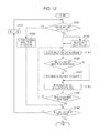
- FIG. 12 is a flowchart of a process performed by the data processor 10 of the third example ( FIG. 11 ).
- FIG. 12 illustrates an exemplary process in which each line of image data constituted by multiple lines is used as a processing unit.
- the checking operation in S 1201 if the data in the Nth line matches the data in the (N ⁇ 1)th line, the result of decoding of the (N ⁇ 1)th line which is stored in the decoded-data memory 10 L is output from the output controller 10 G (S 1202 ). It is checked whether or not all of the lines in the image data have been decoded (S 1006 ). If all of the lines have not been decoded, N is updated to N+1 (S 1007 ), and the next line, i.e., the Nth line (N has been updated), is processed.
Landscapes
- Engineering & Computer Science (AREA)
- Theoretical Computer Science (AREA)
- Compression Of Band Width Or Redundancy In Fax (AREA)
- Compression, Expansion, Code Conversion, And Decoders (AREA)
Abstract
Description
Claims (19)
Applications Claiming Priority (2)
| Application Number | Priority Date | Filing Date | Title |
|---|---|---|---|
| JP2016-038552 | 2016-03-01 | ||
| JP2016038552A JP6623843B2 (en) | 2016-03-01 | 2016-03-01 | Data processing device and program |
Publications (2)
| Publication Number | Publication Date |
|---|---|
| US20170257114A1 US20170257114A1 (en) | 2017-09-07 |
| US9780807B2 true US9780807B2 (en) | 2017-10-03 |
Family
ID=59724403
Family Applications (1)
| Application Number | Title | Priority Date | Filing Date |
|---|---|---|---|
| US15/251,691 Expired - Fee Related US9780807B2 (en) | 2016-03-01 | 2016-08-30 | Data processing apparatus, data processing method, and non-transitory computer readable medium |
Country Status (2)
| Country | Link |
|---|---|
| US (1) | US9780807B2 (en) |
| JP (1) | JP6623843B2 (en) |
Citations (5)
| Publication number | Priority date | Publication date | Assignee | Title |
|---|---|---|---|---|
| US7330137B2 (en) * | 2003-12-12 | 2008-02-12 | Mediatek Inc. | Method and apparatus for RLL code encoding and decoding |
| US7385533B2 (en) * | 2005-03-31 | 2008-06-10 | Fujitsu Limited | Encoder and decoder using run-length-limited code |
| US7565024B2 (en) * | 2003-12-19 | 2009-07-21 | Intel Corporation | Run length coding and decoding |
| JP2011055422A (en) | 2009-09-04 | 2011-03-17 | Canon Inc | Data converting apparatus |
| US8724913B2 (en) * | 2012-07-19 | 2014-05-13 | Omnivision Technologies, Inc. | Decoder and method for decoding run-length-encoded data |
Family Cites Families (6)
| Publication number | Priority date | Publication date | Assignee | Title |
|---|---|---|---|---|
| EP1471520A1 (en) * | 2003-04-22 | 2004-10-27 | Deutsche Thomson-Brandt Gmbh | Method for decoding data received from a data source using hardware configuration data received from the same data source |
| EP1724931A1 (en) * | 2004-03-12 | 2006-11-22 | Matsushita Electric Industrial Co., Ltd. | Variable-length code decoding device |
| JP4642501B2 (en) * | 2005-02-15 | 2011-03-02 | キヤノン株式会社 | Data decoding apparatus, data decoding method, and recording apparatus |
| JP5636816B2 (en) * | 2010-08-25 | 2014-12-10 | 富士ゼロックス株式会社 | Reconfigurable arithmetic circuit and program |
| EP2774371B1 (en) * | 2011-11-03 | 2020-08-26 | Sun Patent Trust | Efficient rounding for deblocking |
| JP5935366B2 (en) * | 2012-02-09 | 2016-06-15 | 富士ゼロックス株式会社 | Image processing device |
-
2016
- 2016-03-01 JP JP2016038552A patent/JP6623843B2/en not_active Expired - Fee Related
- 2016-08-30 US US15/251,691 patent/US9780807B2/en not_active Expired - Fee Related
Patent Citations (5)
| Publication number | Priority date | Publication date | Assignee | Title |
|---|---|---|---|---|
| US7330137B2 (en) * | 2003-12-12 | 2008-02-12 | Mediatek Inc. | Method and apparatus for RLL code encoding and decoding |
| US7565024B2 (en) * | 2003-12-19 | 2009-07-21 | Intel Corporation | Run length coding and decoding |
| US7385533B2 (en) * | 2005-03-31 | 2008-06-10 | Fujitsu Limited | Encoder and decoder using run-length-limited code |
| JP2011055422A (en) | 2009-09-04 | 2011-03-17 | Canon Inc | Data converting apparatus |
| US8724913B2 (en) * | 2012-07-19 | 2014-05-13 | Omnivision Technologies, Inc. | Decoder and method for decoding run-length-encoded data |
Also Published As
| Publication number | Publication date |
|---|---|
| US20170257114A1 (en) | 2017-09-07 |
| JP2017157987A (en) | 2017-09-07 |
| JP6623843B2 (en) | 2019-12-25 |
Similar Documents
| Publication | Publication Date | Title |
|---|---|---|
| KR20060013021A (en) | Content-based Adaptive Binary Arithmetic Decoding Method and Apparatus | |
| US10938412B2 (en) | Decompression of model parameters using functions based upon cumulative count distributions | |
| US8094048B2 (en) | Method of decoding syntax element in context-based adaptive binary arithmetic coding decoder and decoding device therefor | |
| JP2015130640A (en) | Data expander, program, and recording-medium | |
| US20140270554A1 (en) | Image encoding apparatus and image decoding apparatus | |
| US9780807B2 (en) | Data processing apparatus, data processing method, and non-transitory computer readable medium | |
| US9092717B2 (en) | Data processing device and data processing method | |
| Cagnazzo et al. | Mutual information-based context quantization | |
| JP2012005070A (en) | Image data decoding apparatus | |
| JP2019148941A (en) | Image processing device | |
| US9407918B2 (en) | Apparatus and method for coding image, and non-transitory computer readable medium thereof | |
| US10192152B2 (en) | Data processing apparatus, data processing method, and non-transitory computer readable medium | |
| JP6855722B2 (en) | Image processing equipment and programs | |
| US9800760B1 (en) | Fast drawing of unrotated delta row encoded images | |
| JP6226695B2 (en) | Image processing device | |
| JP5732765B2 (en) | Image data decoding device | |
| JP6821184B2 (en) | Image decoder | |
| US10182178B2 (en) | Parallel fast drawing of unrotated delta row encoded images | |
| US20160088187A1 (en) | Data processing apparatus, data processing method, and non-transitory computer readable medium | |
| JP6354360B2 (en) | Conversion device | |
| JP6821183B2 (en) | Image decoder | |
| US9886738B2 (en) | Data processing apparatus and data processing method | |
| JP2007276207A (en) | Printing device and print processing method therefor | |
| Choi et al. | Design of A Multimedia Bitstream ASIP for Multiple CABAC Standards | |
| JP2007088826A (en) | Data processing method and data processing apparatus |
Legal Events
| Date | Code | Title | Description |
|---|---|---|---|
| AS | Assignment |
Owner name: FUJI XEROX CO., LTD., JAPAN Free format text: ASSIGNMENT OF ASSIGNORS INTEREST;ASSIGNORS:KUKIMIYA, RYO;OKUYAMA, JUNICHI;REEL/FRAME:039588/0048 Effective date: 20160812 |
|
| STCF | Information on status: patent grant |
Free format text: PATENTED CASE |
|
| MAFP | Maintenance fee payment |
Free format text: PAYMENT OF MAINTENANCE FEE, 4TH YEAR, LARGE ENTITY (ORIGINAL EVENT CODE: M1551); ENTITY STATUS OF PATENT OWNER: LARGE ENTITY Year of fee payment: 4 |
|
| AS | Assignment |
Owner name: FUJIFILM BUSINESS INNOVATION CORP., JAPAN Free format text: CHANGE OF NAME;ASSIGNOR:FUJI XEROX CO., LTD.;REEL/FRAME:058287/0056 Effective date: 20210401 |
|
| FEPP | Fee payment procedure |
Free format text: MAINTENANCE FEE REMINDER MAILED (ORIGINAL EVENT CODE: REM.); ENTITY STATUS OF PATENT OWNER: LARGE ENTITY |
|
| LAPS | Lapse for failure to pay maintenance fees |
Free format text: PATENT EXPIRED FOR FAILURE TO PAY MAINTENANCE FEES (ORIGINAL EVENT CODE: EXP.); ENTITY STATUS OF PATENT OWNER: LARGE ENTITY |
|
| STCH | Information on status: patent discontinuation |
Free format text: PATENT EXPIRED DUE TO NONPAYMENT OF MAINTENANCE FEES UNDER 37 CFR 1.362 |
|
| FP | Lapsed due to failure to pay maintenance fee |
Effective date: 20251003 |