US9779904B2 - Chip type fuse - Google Patents
Chip type fuse Download PDFInfo
- Publication number
- US9779904B2 US9779904B2 US14/739,119 US201514739119A US9779904B2 US 9779904 B2 US9779904 B2 US 9779904B2 US 201514739119 A US201514739119 A US 201514739119A US 9779904 B2 US9779904 B2 US 9779904B2
- Authority
- US
- United States
- Prior art keywords
- metal layer
- layer
- fuse element
- fuse
- chip type
- Prior art date
- Legal status (The legal status is an assumption and is not a legal conclusion. Google has not performed a legal analysis and makes no representation as to the accuracy of the status listed.)
- Active
Links
Images


Classifications
-
- H—ELECTRICITY
- H01—ELECTRIC ELEMENTS
- H01H—ELECTRIC SWITCHES; RELAYS; SELECTORS; EMERGENCY PROTECTIVE DEVICES
- H01H85/00—Protective devices in which the current flows through a part of fusible material and this current is interrupted by displacement of the fusible material when this current becomes excessive
- H01H85/02—Details
- H01H85/04—Fuses, i.e. expendable parts of the protective device, e.g. cartridges
- H01H85/05—Component parts thereof
- H01H85/055—Fusible members
- H01H85/06—Fusible members characterised by the fusible material
-
- H—ELECTRICITY
- H01—ELECTRIC ELEMENTS
- H01H—ELECTRIC SWITCHES; RELAYS; SELECTORS; EMERGENCY PROTECTIVE DEVICES
- H01H85/00—Protective devices in which the current flows through a part of fusible material and this current is interrupted by displacement of the fusible material when this current becomes excessive
- H01H85/02—Details
- H01H85/04—Fuses, i.e. expendable parts of the protective device, e.g. cartridges
- H01H85/041—Fuses, i.e. expendable parts of the protective device, e.g. cartridges characterised by the type
- H01H85/046—Fuses formed as printed circuits
-
- H—ELECTRICITY
- H01—ELECTRIC ELEMENTS
- H01H—ELECTRIC SWITCHES; RELAYS; SELECTORS; EMERGENCY PROTECTIVE DEVICES
- H01H85/00—Protective devices in which the current flows through a part of fusible material and this current is interrupted by displacement of the fusible material when this current becomes excessive
- H01H85/02—Details
- H01H85/04—Fuses, i.e. expendable parts of the protective device, e.g. cartridges
- H01H85/041—Fuses, i.e. expendable parts of the protective device, e.g. cartridges characterised by the type
- H01H85/0411—Miniature fuses
- H01H2085/0414—Surface mounted fuses
-
- H—ELECTRICITY
- H01—ELECTRIC ELEMENTS
- H01H—ELECTRIC SWITCHES; RELAYS; SELECTORS; EMERGENCY PROTECTIVE DEVICES
- H01H69/00—Apparatus or processes for the manufacture of emergency protective devices
- H01H69/02—Manufacture of fuses
- H01H69/022—Manufacture of fuses of printed circuit fuses
-
- H—ELECTRICITY
- H01—ELECTRIC ELEMENTS
- H01H—ELECTRIC SWITCHES; RELAYS; SELECTORS; EMERGENCY PROTECTIVE DEVICES
- H01H85/00—Protective devices in which the current flows through a part of fusible material and this current is interrupted by displacement of the fusible material when this current becomes excessive
- H01H85/02—Details
- H01H85/04—Fuses, i.e. expendable parts of the protective device, e.g. cartridges
- H01H85/05—Component parts thereof
- H01H85/18—Casing fillings, e.g. powder
- H01H85/185—Insulating members for supporting fusible elements inside a casing, e.g. for helically wound fusible elements
Definitions
- the invention relates to circuit protection elements, particularly chip type fuses having a fuse element, which fuses by a prescribed overcurrent.
- the chip type fuse has previously been known (for example, see laid-open Japanese patent publication 2008-52989).
- the chip type fuse includes an under-glass layer formed on an upper surface of an insulative substrate, a pair of thick film electrodes formed on the glass layer, a fuse element of thin film or thick film formed so as to connect to the thick film electrodes, an over-glass layer formed on the fuse element, and a resin protective layer formed on an upper surface of the glass layer.
- the chip type fuse of the invention includes an insulative substrate; an under-glass layer formed on the insulative substrate; a fuse element formed on the under-glass layer; a pair of electrodes formed at both end sides of the fuse element; and an over-glass layer covering at least a fusing section of the fuse element; wherein the fuse element includes a layer where a first metal layer and a second metal layer are piled up, and a barrier layer consisting of a third metal layer, which covers the first metal layer and the second metal layer with a width that is wider than the width of the first metal layer and the second metal layer.
- the barrier layer can control this movement, thus resistance to heat can be improved. Therefore, the chip type fuse excellent in resistance to climatic conditions, which operates stably in high temperature and high humidity environments, can be obtained.
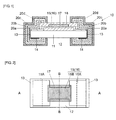
- FIG. 2 is a plan view of the chip type fuse of FIG. 1 after forming the over-glass layer.
- FIG. 3 is a plan view of the chip type fuse of FIG. 1 after forming protective resin layer.
- FIG. 4 is an enlarged cross-sectional view of the chip type fuse along BB lines in FIG. 2 and FIG. 3 .
- FIG. 5 is a graph showing a result of 85° C./85% humidity/power on testing performed on chip type fuses and a prior art structure.
- FIG. 6 is a graph showing a result of 175° C. resistance to heat storage testing performed on chip type fuses and a prior art structure.
- FIG. 7 is a graph showing a result of 134° C./95% humidity and power on testing performed on chip type fuses and a prior art structure.
- the fuse element layer 15 includes a barrier layer 16 consisting of the third metal layer, which covers the first metal layer 15 a and the second metal layer 15 b with width that is wider than the width of the first metal layer 15 a and the second metal layer 15 b . That is, the barrier layer 16 consisting of the third metal layer overwraps the second metal layer 15 b and the first metal layer 15 a (see FIG. 4 ).
- the fuse element 15 includes the first metal layer 15 a , the second metal layer 15 b , and the barrier metal layer 16 .
- the third metal layer as the barrier layer 16 preferably consists of Ta or Cr, and is formed by sputtering. However, Ni, NiCr(6:4), NiCr(8:2), or Ti, etc. demonstrates a barrier effect, and can be used as the barrier layer. It is preferable that the film thickness of the barrier layer 16 is in range of 50-2000 ⁇ .
- the protection layer 18 consisting of epoxy resin etc. is disposed at an upper side of the over-glass layer 17 .
- the end face electrodes 13 connecting front electrode 15 A and rear electrode 14 is formed at end face of insulative substrate 11 .
- the plated electrode layers 20 a , 20 b , 20 c , 20 d which are suitable for surface mounting, are formed on exposed surfaces of end face electrodes and front and rear electrodes 13 , 15 A, 14 (see FIG. 1 and FIG. 2 ).
- Plated electrode layer 20 a consists of Ni plated layer
- plated electrode layer 20 b consists of Cu plated layer
- plated electrode layer 20 c consists of Ni plated layer
- plated electrode layer 20 d consists of Sn plated layer.
- Such a structure is similar to usual chip type parts, thus the chip type fuse 10 comprises such chip type parts, and thereby is available for surface mounting.
- Low melting point glass is used for over-glass layer 17 , because of the restriction that the later processes must be performed at a lower temperature.
- the low melting point glass contains components such as boron, lead, or bismuth etc. for lowering the melting point.
- One of these typical components is a borosilicate glass.
- the borosilicate glass takes moisture in under a humidity environment. The following reactions take place for producing boric acid (H3BO3), which corrodes Cu. Then the fuse element consisting of Cu corrodes under the high humidity environment.
- barrier layer 16 guards against the interaction of water molecules with Cu in the fuse element layer 15 , corrosion by moisture intrusion to Cu is prevented and resistance to humidity can be improved.
- the barrier layer 16 is formed so as to cap the surface and to stop movement of Cu particles on the fuse element. Therefore, because of the barrier layer 16 , the transfer phenomenon etc. of Cu is prevented, and resistance to heat can be improved. As a result, because the barrier layer 16 can be effective to two kinds of failure mechanisms, the barrier layer 16 can improve resistance to humidity and resistance to high temperature, and an excellent chip type fuse resistant to climatic conditions is obtained.
- FIG. 5 shows a result of 85° C. temperature/85% humidity/power on test.
- the test was carried out on samples including the barrier layer 16 and a prior art structure.
- the barrier layer 16 being Ta or Cr
- domination of resistance to climatic conditions has been confirmed to the prior art structure (no barrier layer). That is, samples were extracted after the test, and whether corrosion of fuse element layer 15 had been caused or not was confirmed.
- the prior art structure had corrosion portions on the fuse element as a result.
- the barrier layer 16 consisting of Ta or Cr both thickness: 250 ⁇
- the barrier layer 16 consisting of Ni did not exhibit corrosion, confirming the effect of such a barrier layer.
- a barrier layer 16 consisting of Ni, NiCr(6:4), NiCr(8:2), or Ti is utilized, the results indicate that resistance to humidity improves.
- barrier layer 16 consists of Cr, or Ta
- barrier layer 16 it is more effective for preventing the particle movement phenomenon on the Cu surface under a high temperature environment.
- barrier layer 16 consisting of Cr or Ta both 250 ⁇
- the activity of Cu particles in the fuse element layer can be decreased, and thereby long-term operation characteristic can be improved.
- the Ta sample demonstrated similar results. The samples were extracted and the fuse elements were observed. As to the barrier layer structure of the above materials, particle movement phenomenon on the Cu surface was not found. From the above testing, the effect of improving resistance at high temperature by including the barrier layer structure has been confirmed.
- FIG. 7 shows the result of a PCT test.
- the PCT test is an abbreviation of “pressure”, “cooker”, “test”, and is a simulated accelerated life test. It is a severe test that impresses 8% of ratings current under a temperature of 134° C. in a pressurized steam atmosphere of 95% humidity. As a result, by extremely increasing the pressure of water vapor inside of the test chamber simulation of infiltration of moisture into a device can be performed in a shortened time.
- the barrier layer Cr750 ⁇ sample ( ⁇ mark) and barrier layer Ti1500 ⁇ sample demonstrated the least resistance change
- the barrier layer Ta750 ⁇ sample ( ⁇ mark) demonstrated a slightly greater change.
- the barrier layer Ni1500 ⁇ ( ⁇ mark) sample demonstrated a greater resistance change than the above samples
- the barrier layer Ni750 ⁇ sample demonstrates a slightly greater change than the Ni1500 ⁇ sample.
- the resistance change ( ⁇ R) of any sample having a barrier layer was less than that of the prior art structure (no barrier layer).
- barrier layer resistance to climatic conditions on the chip type fuse can be improved, and a thin film such as Cr, Ta, or Ti etc. is especially effective as the barrier layer.
- a thin film such as Cr, Ta, or Ti etc.
- Ni, NiCr(6:4), and NiCr(8:2), etc. were studied. The movement of Cu particles is not observed upon these devices. And, it is thought that resistance change ( ⁇ R) of these materials is less than that of a prior art structure as shown in FIG. 7 , and these materials are also effective as the barrier layer.
- the invention can be suitably used for chip type circuit protection elements, especially for chip type fuses.
Abstract
A chip type fuse excellent in resistance to climate conditions, where the fuse is able to operate stably under high temperature and high humidity environments. The fuse includes an insulative substrate; an under-glass layer formed on the insulative substrate; a fuse element formed on the under-glass layer; a pair of electrodes formed at both end sides of the fuse element; and an over-glass layer covering at least a fusing section of the fuse element; wherein the fuse element includes a layer where a first metal layer and a second metal layer are piled up, and a barrier layer consisting of a third metal layer, which covers the first metal layer and the second metal layer with a width that is wider than the width of the first metal layer and the second metal layer. The third metal layer overwraps the second metal layer and the first metal layer.
Description
The invention relates to circuit protection elements, particularly chip type fuses having a fuse element, which fuses by a prescribed overcurrent.
The chip type fuse has previously been known (for example, see laid-open Japanese patent publication 2008-52989). The chip type fuse includes an under-glass layer formed on an upper surface of an insulative substrate, a pair of thick film electrodes formed on the glass layer, a fuse element of thin film or thick film formed so as to connect to the thick film electrodes, an over-glass layer formed on the fuse element, and a resin protective layer formed on an upper surface of the glass layer.
Within such a chip type fuse, because the fuse element is covered by under and over glass layers, an effect that heat from the fuse element is stored therein is caused, and the fuse element can be fused with a small overcurrent at high speed.
In the chip type fuse, the fuse element is covered by the glass layers on both sides for improving fusing characteristics based on an assumption of reaction with dry gaseous oxygen in the atmosphere. However, under a high humidity environment, there is a problem that boric oxide of the glass element becomes boric acid, which in turn melts on the fuse element, thereby corroding the fuse element pattern of Cu. Additionally, because the fuse element pattern is formed by Cu on its surface, movement of Cu is promoted when exposed to a high temperature environment, which may result in upheaval of Cu along a grain boundary. Thus there is a possibility that the fuse element may be damaged by long term use in a high humidity and/or high temperature environment.
The current invention has been made based on the above-mentioned circumstances. Therefore an object of the invention is to provide a chip type fuse excellent in resistance to climate conditions, whereby the fuse is able to operate stably under high temperature and high humidity environments.
The chip type fuse of the invention includes an insulative substrate; an under-glass layer formed on the insulative substrate; a fuse element formed on the under-glass layer; a pair of electrodes formed at both end sides of the fuse element; and an over-glass layer covering at least a fusing section of the fuse element; wherein the fuse element includes a layer where a first metal layer and a second metal layer are piled up, and a barrier layer consisting of a third metal layer, which covers the first metal layer and the second metal layer with a width that is wider than the width of the first metal layer and the second metal layer.
Though, there was a problem that over-glass layer includes borosilicate glass that contains boron for lowering melting point, boric oxide of the glass layer becomes boric acid in high temperature and high humidity environments, and it begins to melt on the fuse element, and corrode the fuse element pattern of Cu etc. According to the invention, because the chip type fuse includes a barrier layer consisting of a third metal layer, which covers the fuse element pattern, thereby the fuse element pattern can be prevented from being corroded.
Further, though a metal layer of the Cu, etc. excellent in conductivity tends to become fluid in the fuse element in a high temperature environment, the barrier layer can control this movement, thus resistance to heat can be improved. Therefore, the chip type fuse excellent in resistance to climatic conditions, which operates stably in high temperature and high humidity environments, can be obtained.
Embodiments of the invention will be described below referring to FIG. 1 through FIG. 7 . Like or corresponding parts or elements will be denoted and explained by same reference characters throughout views.
The fuse element 15 consists of first metal layer 15 a formed by sputtering and second metal layer 15 b also formed by sputtering piled up on the layer 15 a. First metal layer 15 a consists of a Cr layer having a film thickness of, for instance, about 500 Å, and second metal layer 15 b consists of a Cu layer having a film thickness of, for instance, about 1-3 μm. Here, the current flows mainly through the second metal layer consisting of the Cu layer of higher conductivity. And, the first metal layer 15 a mainly plays the role to connect the second metal layer 15 b on the under-glass layer 12.
The fuse element layer 15 includes a barrier layer 16 consisting of the third metal layer, which covers the first metal layer 15 a and the second metal layer 15 b with width that is wider than the width of the first metal layer 15 a and the second metal layer 15 b. That is, the barrier layer 16 consisting of the third metal layer overwraps the second metal layer 15 b and the first metal layer 15 a (see FIG. 4 ). In this embodiment, the fuse element 15 includes the first metal layer 15 a, the second metal layer 15 b, and the barrier metal layer 16. The third metal layer as the barrier layer 16 preferably consists of Ta or Cr, and is formed by sputtering. However, Ni, NiCr(6:4), NiCr(8:2), or Ti, etc. demonstrates a barrier effect, and can be used as the barrier layer. It is preferable that the film thickness of the barrier layer 16 is in range of 50-2000 Å.
Over-glass layer 17, has a width narrower than a width of electrode section 15A, and is formed at an area for covering the fusing section (fuse element) 15B of the fuse element 15. Accordingly four surfaces of the second metal layer 15 b consisting of Cu, which becomes the main current route, are surrounded by barrier layer 16 consisting of Ta or Cr etc. and first metal layer 15 a consisting of Cr. Further, the fuse element 15 consisting of first and second metal layers and the barrier layer 16 consisting of third metal layer are surrounded by under-glass layer 12 and over-glass layer 17 (see FIG. 4 ).
The protection layer 18 consisting of epoxy resin etc. is disposed at an upper side of the over-glass layer 17. The end face electrodes 13 connecting front electrode 15A and rear electrode 14 is formed at end face of insulative substrate 11. The plated electrode layers 20 a, 20 b, 20 c, 20 d, which are suitable for surface mounting, are formed on exposed surfaces of end face electrodes and front and rear electrodes 13, 15A, 14 (see FIG. 1 and FIG. 2 ). Plated electrode layer 20 a consists of Ni plated layer, plated electrode layer 20 b consists of Cu plated layer, plated electrode layer 20 c consists of Ni plated layer, and plated electrode layer 20 d consists of Sn plated layer. Such a structure is similar to usual chip type parts, thus the chip type fuse 10 comprises such chip type parts, and thereby is available for surface mounting.
Low melting point glass is used for over-glass layer 17, because of the restriction that the later processes must be performed at a lower temperature. In general, the low melting point glass contains components such as boron, lead, or bismuth etc. for lowering the melting point. One of these typical components is a borosilicate glass. The borosilicate glass takes moisture in under a humidity environment. The following reactions take place for producing boric acid (H3BO3), which corrodes Cu. Then the fuse element consisting of Cu corrodes under the high humidity environment.
B2O3(glass)+3H2O→2H3BO3(boric acid)
CuO+2H3BO3(boric acid)→Cu(BO2)2+3H2O
B2O3(glass)+3H2O→2H3BO3(boric acid)
CuO+2H3BO3(boric acid)→Cu(BO2)2+3H2O
That is, in the high humidity environment, an outside water molecule (moisture) enters into the product and when it reaches the fuse element, the fuse element corrodes by the oxidation action between moisture and boron components. Such a mechanism can be assumed. Therefore, because barrier layer 16 guards against the interaction of water molecules with Cu in the fuse element layer 15, corrosion by moisture intrusion to Cu is prevented and resistance to humidity can be improved.
Further, in the high temperature environment, Cu particles in the fuse element 15 are activated by the thermal energy, and thereby become more fluid. Accordingly, because Cu particles on a surface of the fuse element tend to cause a transfer phenomenon, the barrier layer 16 is formed so as to cap the surface and to stop movement of Cu particles on the fuse element. Therefore, because of the barrier layer 16, the transfer phenomenon etc. of Cu is prevented, and resistance to heat can be improved. As a result, because the barrier layer 16 can be effective to two kinds of failure mechanisms, the barrier layer 16 can improve resistance to humidity and resistance to high temperature, and an excellent chip type fuse resistant to climatic conditions is obtained.
In the case of carrying out the resistance to climatic condition test, the prior art structure (no barrier layer), had corrosion portions on the fuse element as a result. However, the barrier layer 16 consisting of Ta or Cr (both thickness: 250 Å), did not have corrosion as a result and change in the resistance value was minor, t thereby confirming the effect of the barrier layer. Further, a barrier layer 16 consisting of Ni (thickness: 333 Å) did not exhibit corrosion, confirming the effect of such a barrier layer. Also, when a barrier layer 16 consisting of Ni, NiCr(6:4), NiCr(8:2), or Ti, is utilized, the results indicate that resistance to humidity improves.
On the other hand, when the barrier layer 16 consists of Cr, or Ta, it is more effective for preventing the particle movement phenomenon on the Cu surface under a high temperature environment. By forming barrier layer 16 consisting of Cr or Ta (both 250 Å) on a surface of the fuse element layer 15 consisting of Cu, the activity of Cu particles in the fuse element layer can be decreased, and thereby long-term operation characteristic can be improved.
In order to confirm the above, five kinds of samples (a prior art structure and barrier layer structures, with the following characteristics, Ni (66 Å), Ni (333 Å), Ta(250 Å), and Cr(250 Å)) were made. And, the samples were left in a 175° C. environmental chamber, and ΔR (resistance change) was observed (see FIG. 6 ). After 1000 hours passed, the prior art structure (no barrier layer), exhibited a resistance change substantially larger (Max.=5.5%) that the samples having a barrier layer structure.
The best material for the barrier layer was Cr, which demonstrated a small resistance change (Max.=1.11%). The Ta sample demonstrated similar results. The samples were extracted and the fuse elements were observed. As to the barrier layer structure of the above materials, particle movement phenomenon on the Cu surface was not found. From the above testing, the effect of improving resistance at high temperature by including the barrier layer structure has been confirmed.
As to resistance change (ΔR) after 50 hours or more passed, the barrier layer Cr750 Å sample (●mark) and barrier layer Ti1500 Å sample demonstrated the least resistance change, Next, the barrier layer Ta750 Å sample (♦mark) demonstrated a slightly greater change. The barrier layer Ni1500 Å(▪mark) sample demonstrated a greater resistance change than the above samples, and the barrier layer Ni750 Å sample demonstrates a slightly greater change than the Ni1500 Å sample. However, the resistance change (ΔR) of any sample having a barrier layer was less than that of the prior art structure (no barrier layer).
As demonstrated above, by including the barrier layer, resistance to climatic conditions on the chip type fuse can be improved, and a thin film such as Cr, Ta, or Ti etc. is especially effective as the barrier layer. Moreover, Ni, NiCr(6:4), and NiCr(8:2), etc. were studied. The movement of Cu particles is not observed upon these devices. And, it is thought that resistance change (ΔR) of these materials is less than that of a prior art structure as shown in FIG. 7 , and these materials are also effective as the barrier layer.
Although embodiments of the invention are explained above, the invention is not limited to the above embodiments, and various changes and modifications may be made within the scope of the technical concepts of the invention.
The invention can be suitably used for chip type circuit protection elements, especially for chip type fuses.
Claims (3)
1. A chip type fuse, comprising:
an insulative substrate;
an under-glass layer formed on the insulative substrate;
a fuse element formed on the under-glass layer;
a pair of electrodes formed at both end sides of the fuse element; and
an over-glass layer covering at least a fusing section of the fuse element;
wherein the fuse element includes a layer where a first metal layer and a second metal layer are piled up, and a barrier layer consisting of a third metal layer, which covers the first metal layer and the second metal layer with width that is wider than the width of the first metal layer and the second metal layer, and
wherein the second metal layer consisting of Cu, which becomes main current route, is surrounded by the barrier layer consisting of any one of Ta, Cr, Ni, NiCr, or Ti and the first metal layer consisting of Cr.
2. The chip type fuse of claim 1 , wherein the second metal layer is positioned between the first metal layer and the third metal layer.
3. The chip type fuse of claim 1 , wherein thickness of the barrier layer is in the range of 50-2000 Å.
Applications Claiming Priority (2)
| Application Number | Priority Date | Filing Date | Title |
|---|---|---|---|
| JP2014-126036 | 2014-06-19 | ||
| JP2014126036A JP6294165B2 (en) | 2014-06-19 | 2014-06-19 | Chip type fuse |
Publications (2)
| Publication Number | Publication Date |
|---|---|
| US20150371804A1 US20150371804A1 (en) | 2015-12-24 |
| US9779904B2 true US9779904B2 (en) | 2017-10-03 |
Family
ID=54870283
Family Applications (1)
| Application Number | Title | Priority Date | Filing Date |
|---|---|---|---|
| US14/739,119 Active US9779904B2 (en) | 2014-06-19 | 2015-06-15 | Chip type fuse |
Country Status (2)
| Country | Link |
|---|---|
| US (1) | US9779904B2 (en) |
| JP (1) | JP6294165B2 (en) |
Cited By (1)
| Publication number | Priority date | Publication date | Assignee | Title |
|---|---|---|---|---|
| US20230420209A1 (en) * | 2022-06-22 | 2023-12-28 | Littelfuse, Inc. | Step-terminated smd fuse |
Families Citing this family (1)
| Publication number | Priority date | Publication date | Assignee | Title |
|---|---|---|---|---|
| JP7154907B2 (en) * | 2018-09-14 | 2022-10-18 | 株式会社東芝 | semiconductor module |
Citations (30)
| Publication number | Priority date | Publication date | Assignee | Title |
|---|---|---|---|---|
| US2911504A (en) * | 1958-05-15 | 1959-11-03 | Sigmund Cohn Corp | Fuse member and method of making the same |
| US4140988A (en) * | 1977-08-04 | 1979-02-20 | Gould Inc. | Electric fuse for small current intensities |
| US4246563A (en) * | 1977-05-28 | 1981-01-20 | Aktieselkabet Laur. Knudsen Nordisk Electricitets | Electric safety fuse |
| US4315235A (en) * | 1980-07-31 | 1982-02-09 | Jacobs Jr Philip C | Composite fusible element for electric current-limiting fuses |
| US4320374A (en) * | 1979-03-21 | 1982-03-16 | Kearney-National (Canada) Limited | Electric fuses employing composite aluminum and cadmium fuse elements |
| JPH0465046A (en) * | 1990-07-02 | 1992-03-02 | Tateyama Kagaku Kogyo Kk | Chip-type fuse resistor |
| US5166656A (en) * | 1992-02-28 | 1992-11-24 | Avx Corporation | Thin film surface mount fuses |
| US5432378A (en) * | 1993-12-15 | 1995-07-11 | Cooper Industries, Inc. | Subminiature surface mounted circuit protector |
| US5546066A (en) * | 1993-08-27 | 1996-08-13 | Yazaki Corporation | Delayed-fusion fuse |
| US5572181A (en) * | 1993-04-30 | 1996-11-05 | Koa Kabushiki Kaisha | Overcurrent protection device |
| US5668522A (en) * | 1993-10-28 | 1997-09-16 | Yazaki Corporation | Slowly-breaking fuse and method of production |
| US5914649A (en) * | 1997-03-28 | 1999-06-22 | Hitachi Chemical Company, Ltd. | Chip fuse and process for production thereof |
| US5929741A (en) * | 1994-11-30 | 1999-07-27 | Hitachi Chemical Company, Ltd. | Current protector |
| US6034589A (en) * | 1998-12-17 | 2000-03-07 | Aem, Inc. | Multi-layer and multi-element monolithic surface mount fuse and method of making the same |
| US6384708B1 (en) * | 1997-09-04 | 2002-05-07 | Wickmann-Werke Gmbh | Electrical fuse element |
| US6452475B1 (en) * | 1999-04-16 | 2002-09-17 | Sony Chemicals Corp. | Protective device |
| US6566995B2 (en) * | 2000-05-17 | 2003-05-20 | Sony Chemicals Corporation | Protective element |
| US6622375B1 (en) * | 1997-12-16 | 2003-09-23 | Yazaki Corporation | Method for producing a fuse element |
| US20040169578A1 (en) * | 2001-06-11 | 2004-09-02 | Andre Jollenbeck | Fuse component |
| US6838971B2 (en) * | 2001-05-21 | 2005-01-04 | Matsushita Electric Industrial Co., Ltd. | Thermal fuse |
| US7116208B2 (en) * | 2000-03-14 | 2006-10-03 | Rohm Co., Ltd. | Printed-circuit board with fuse |
| JP2008052989A (en) | 2006-08-23 | 2008-03-06 | Koa Corp | Chip type circuit protection element |
| US20080191832A1 (en) * | 2007-02-14 | 2008-08-14 | Besdon Technology Corporation | Chip-type fuse and method of manufacturing the same |
| US7570148B2 (en) * | 2002-01-10 | 2009-08-04 | Cooper Technologies Company | Low resistance polymer matrix fuse apparatus and method |
| US20110163840A1 (en) * | 2008-10-28 | 2011-07-07 | Nanjing Sart Science & Technology Development Co., Ltd. | High reliability blade fuse and the manufacturing method thereof |
| US8081057B2 (en) * | 2009-05-14 | 2011-12-20 | Hung-Chih Chiu | Current protection device and the method for forming the same |
| WO2013059604A1 (en) * | 2011-10-19 | 2013-04-25 | Littelfuse, Inc. | Composite fuse element and method of making |
| WO2013166788A1 (en) * | 2012-05-10 | 2013-11-14 | 苏州晶讯科技股份有限公司 | Surface-mounted fuse |
| US8957755B2 (en) * | 2008-11-25 | 2015-02-17 | Nanjing Sart Science & Technology Development Co., Ltd. | Multi-layer blade fuse and the manufacturing method thereof |
| US9035740B2 (en) * | 2007-11-08 | 2015-05-19 | Panasonic Intellectual Property Management Co., Ltd. | Circuit protective device and method for manufacturing the same |
Family Cites Families (5)
| Publication number | Priority date | Publication date | Assignee | Title |
|---|---|---|---|---|
| JPH09129115A (en) * | 1995-10-30 | 1997-05-16 | Kyocera Corp | Chip fuse |
| JP4632358B2 (en) * | 2005-06-08 | 2011-02-16 | 三菱マテリアル株式会社 | Chip type fuse |
| JP4716099B2 (en) * | 2005-09-30 | 2011-07-06 | 三菱マテリアル株式会社 | Manufacturing method of chip-type fuse |
| US9847203B2 (en) * | 2010-10-14 | 2017-12-19 | Avx Corporation | Low current fuse |
| JP6249600B2 (en) * | 2012-03-29 | 2017-12-20 | デクセリアルズ株式会社 | Protective element |
-
2014
- 2014-06-19 JP JP2014126036A patent/JP6294165B2/en active Active
-
2015
- 2015-06-15 US US14/739,119 patent/US9779904B2/en active Active
Patent Citations (30)
| Publication number | Priority date | Publication date | Assignee | Title |
|---|---|---|---|---|
| US2911504A (en) * | 1958-05-15 | 1959-11-03 | Sigmund Cohn Corp | Fuse member and method of making the same |
| US4246563A (en) * | 1977-05-28 | 1981-01-20 | Aktieselkabet Laur. Knudsen Nordisk Electricitets | Electric safety fuse |
| US4140988A (en) * | 1977-08-04 | 1979-02-20 | Gould Inc. | Electric fuse for small current intensities |
| US4320374A (en) * | 1979-03-21 | 1982-03-16 | Kearney-National (Canada) Limited | Electric fuses employing composite aluminum and cadmium fuse elements |
| US4315235A (en) * | 1980-07-31 | 1982-02-09 | Jacobs Jr Philip C | Composite fusible element for electric current-limiting fuses |
| JPH0465046A (en) * | 1990-07-02 | 1992-03-02 | Tateyama Kagaku Kogyo Kk | Chip-type fuse resistor |
| US5166656A (en) * | 1992-02-28 | 1992-11-24 | Avx Corporation | Thin film surface mount fuses |
| US5572181A (en) * | 1993-04-30 | 1996-11-05 | Koa Kabushiki Kaisha | Overcurrent protection device |
| US5546066A (en) * | 1993-08-27 | 1996-08-13 | Yazaki Corporation | Delayed-fusion fuse |
| US5668522A (en) * | 1993-10-28 | 1997-09-16 | Yazaki Corporation | Slowly-breaking fuse and method of production |
| US5432378A (en) * | 1993-12-15 | 1995-07-11 | Cooper Industries, Inc. | Subminiature surface mounted circuit protector |
| US5929741A (en) * | 1994-11-30 | 1999-07-27 | Hitachi Chemical Company, Ltd. | Current protector |
| US5914649A (en) * | 1997-03-28 | 1999-06-22 | Hitachi Chemical Company, Ltd. | Chip fuse and process for production thereof |
| US6384708B1 (en) * | 1997-09-04 | 2002-05-07 | Wickmann-Werke Gmbh | Electrical fuse element |
| US6622375B1 (en) * | 1997-12-16 | 2003-09-23 | Yazaki Corporation | Method for producing a fuse element |
| US6034589A (en) * | 1998-12-17 | 2000-03-07 | Aem, Inc. | Multi-layer and multi-element monolithic surface mount fuse and method of making the same |
| US6452475B1 (en) * | 1999-04-16 | 2002-09-17 | Sony Chemicals Corp. | Protective device |
| US7116208B2 (en) * | 2000-03-14 | 2006-10-03 | Rohm Co., Ltd. | Printed-circuit board with fuse |
| US6566995B2 (en) * | 2000-05-17 | 2003-05-20 | Sony Chemicals Corporation | Protective element |
| US6838971B2 (en) * | 2001-05-21 | 2005-01-04 | Matsushita Electric Industrial Co., Ltd. | Thermal fuse |
| US20040169578A1 (en) * | 2001-06-11 | 2004-09-02 | Andre Jollenbeck | Fuse component |
| US7570148B2 (en) * | 2002-01-10 | 2009-08-04 | Cooper Technologies Company | Low resistance polymer matrix fuse apparatus and method |
| JP2008052989A (en) | 2006-08-23 | 2008-03-06 | Koa Corp | Chip type circuit protection element |
| US20080191832A1 (en) * | 2007-02-14 | 2008-08-14 | Besdon Technology Corporation | Chip-type fuse and method of manufacturing the same |
| US9035740B2 (en) * | 2007-11-08 | 2015-05-19 | Panasonic Intellectual Property Management Co., Ltd. | Circuit protective device and method for manufacturing the same |
| US20110163840A1 (en) * | 2008-10-28 | 2011-07-07 | Nanjing Sart Science & Technology Development Co., Ltd. | High reliability blade fuse and the manufacturing method thereof |
| US8957755B2 (en) * | 2008-11-25 | 2015-02-17 | Nanjing Sart Science & Technology Development Co., Ltd. | Multi-layer blade fuse and the manufacturing method thereof |
| US8081057B2 (en) * | 2009-05-14 | 2011-12-20 | Hung-Chih Chiu | Current protection device and the method for forming the same |
| WO2013059604A1 (en) * | 2011-10-19 | 2013-04-25 | Littelfuse, Inc. | Composite fuse element and method of making |
| WO2013166788A1 (en) * | 2012-05-10 | 2013-11-14 | 苏州晶讯科技股份有限公司 | Surface-mounted fuse |
Non-Patent Citations (1)
| Title |
|---|
| JP 2008-52989, Mar. 2008, English machine translation. * |
Cited By (2)
| Publication number | Priority date | Publication date | Assignee | Title |
|---|---|---|---|---|
| US20230420209A1 (en) * | 2022-06-22 | 2023-12-28 | Littelfuse, Inc. | Step-terminated smd fuse |
| US11923162B2 (en) * | 2022-06-22 | 2024-03-05 | Littelfuse, Inc. | Step-terminated SMD fuse |
Also Published As
| Publication number | Publication date |
|---|---|
| JP2016004736A (en) | 2016-01-12 |
| US20150371804A1 (en) | 2015-12-24 |
| JP6294165B2 (en) | 2018-03-14 |
Similar Documents
| Publication | Publication Date | Title |
|---|---|---|
| US10937619B2 (en) | Fuse element and fuse device | |
| CN101514457B (en) | Multi-purpose metal surface protectant and preparation method thereof | |
| US9779904B2 (en) | Chip type fuse | |
| KR20140050573A (en) | Low current fuse | |
| CN107403763B (en) | Chip packing-body and the method for forming chip packing-body | |
| US9831054B2 (en) | Insulated thermal cut-off device | |
| JPH01248538A (en) | Semiconductor device | |
| US9291543B1 (en) | PC board mount corrosion sensitive sensor | |
| KR20190051016A (en) | Corrosion monitoring device | |
| WO2019116814A1 (en) | Chip resistor | |
| JP2007059295A (en) | Circuit protective element and protection method of circuit | |
| JP2006515716A (en) | Sealing body for organic electronic device and method for manufacturing the sealing body | |
| JP2020165749A (en) | Corrosion sensor and structure equipped therewith | |
| JPH0412428A (en) | Fuse element | |
| JP7401387B2 (en) | Corrosion environment monitoring device | |
| RU2513654C2 (en) | Resistance thermometer | |
| JP7220344B2 (en) | circuit protection element | |
| US20200111942A1 (en) | Corrosion resistant thermoelectric devices | |
| KR102556009B1 (en) | Filler structure and the electric device including the same | |
| JP2020129602A (en) | Resistor | |
| JPS6246938B2 (en) | ||
| US20050280497A1 (en) | Fuse with metallic state indicator | |
| SE1150101A1 (en) | Material for providing an electrically conductive contact layer, a contact element with such layer, method for providing the contact element, and use of the material | |
| Sparling | Corrosion prevention/deterioration control in electronic components and assemblies | |
| CN205767830U (en) | A kind of internal energising plate |
Legal Events
| Date | Code | Title | Description |
|---|---|---|---|
| AS | Assignment |
Owner name: KOA CORPORATION, JAPAN Free format text: ASSIGNMENT OF ASSIGNORS INTEREST;ASSIGNORS:ISHIKAWA, TAKAHIRO;ICHIKAWA, HIROSHI;ITO, CHIKA;REEL/FRAME:035836/0694 Effective date: 20150602 |
|
| STCF | Information on status: patent grant |
Free format text: PATENTED CASE |
|
| MAFP | Maintenance fee payment |
Free format text: PAYMENT OF MAINTENANCE FEE, 4TH YEAR, LARGE ENTITY (ORIGINAL EVENT CODE: M1551); ENTITY STATUS OF PATENT OWNER: LARGE ENTITY Year of fee payment: 4 |