US9735850B2 - High linearity antenna swapping circuitry - Google Patents

High linearity antenna swapping circuitry Download PDF

Info

Publication number
US9735850B2
US9735850B2 US15/084,142 US201615084142A US9735850B2 US 9735850 B2 US9735850 B2 US 9735850B2 US 201615084142 A US201615084142 A US 201615084142A US 9735850 B2 US9735850 B2 US 9735850B2
Authority
US
United States
Prior art keywords
circuitry
switching element
band
low
switching
Prior art date
Legal status (The legal status is an assumption and is not a legal conclusion. Google has not performed a legal analysis and makes no representation as to the accuracy of the status listed.)
Active
Application number
US15/084,142
Other versions
US20160373176A1 (en
Inventor
Nadim Khlat
Marcus Granger-Jones
Current Assignee (The listed assignees may be inaccurate. Google has not performed a legal analysis and makes no representation or warranty as to the accuracy of the list.)
RF Micro Devices Inc
Qorvo US Inc
Original Assignee
Qorvo US Inc
Priority date (The priority date is an assumption and is not a legal conclusion. Google has not performed a legal analysis and makes no representation as to the accuracy of the date listed.)
Filing date
Publication date
Application filed by Qorvo US Inc filed Critical Qorvo US Inc
Priority to US15/084,142 priority Critical patent/US9735850B2/en
Assigned to RF MICRO DEVICES, INC. reassignment RF MICRO DEVICES, INC. ASSIGNMENT OF ASSIGNORS INTEREST (SEE DOCUMENT FOR DETAILS). Assignors: KHLAT, NADIM, GRANGER-JONES, MARCUS
Assigned to QORVO US, INC. reassignment QORVO US, INC. MERGER (SEE DOCUMENT FOR DETAILS). Assignors: RF MICRO DEVICES, INC.
Publication of US20160373176A1 publication Critical patent/US20160373176A1/en
Application granted granted Critical
Publication of US9735850B2 publication Critical patent/US9735850B2/en
Active legal-status Critical Current
Anticipated expiration legal-status Critical

Links

Images

Classifications

    • HELECTRICITY
    • H04ELECTRIC COMMUNICATION TECHNIQUE
    • H04BTRANSMISSION
    • H04B7/00Radio transmission systems, i.e. using radiation field
    • H04B7/02Diversity systems; Multi-antenna system, i.e. transmission or reception using multiple antennas
    • H04B7/04Diversity systems; Multi-antenna system, i.e. transmission or reception using multiple antennas using two or more spaced independent antennas
    • H04B7/06Diversity systems; Multi-antenna system, i.e. transmission or reception using multiple antennas using two or more spaced independent antennas at the transmitting station
    • H04B7/0602Diversity systems; Multi-antenna system, i.e. transmission or reception using multiple antennas using two or more spaced independent antennas at the transmitting station using antenna switching
    • H04B7/0608Antenna selection according to transmission parameters
    • HELECTRICITY
    • H04ELECTRIC COMMUNICATION TECHNIQUE
    • H04BTRANSMISSION
    • H04B1/00Details of transmission systems, not covered by a single one of groups H04B3/00 - H04B13/00; Details of transmission systems not characterised by the medium used for transmission
    • H04B1/005Details of transmission systems, not covered by a single one of groups H04B3/00 - H04B13/00; Details of transmission systems not characterised by the medium used for transmission adapting radio receivers, transmitters andtransceivers for operation on two or more bands, i.e. frequency ranges
    • H04B1/0053Details of transmission systems, not covered by a single one of groups H04B3/00 - H04B13/00; Details of transmission systems not characterised by the medium used for transmission adapting radio receivers, transmitters andtransceivers for operation on two or more bands, i.e. frequency ranges with common antenna for more than one band
    • HELECTRICITY
    • H04ELECTRIC COMMUNICATION TECHNIQUE
    • H04BTRANSMISSION
    • H04B1/00Details of transmission systems, not covered by a single one of groups H04B3/00 - H04B13/00; Details of transmission systems not characterised by the medium used for transmission
    • H04B1/005Details of transmission systems, not covered by a single one of groups H04B3/00 - H04B13/00; Details of transmission systems not characterised by the medium used for transmission adapting radio receivers, transmitters andtransceivers for operation on two or more bands, i.e. frequency ranges
    • H04B1/0064Details of transmission systems, not covered by a single one of groups H04B3/00 - H04B13/00; Details of transmission systems not characterised by the medium used for transmission adapting radio receivers, transmitters andtransceivers for operation on two or more bands, i.e. frequency ranges with separate antennas for the more than one band
    • HELECTRICITY
    • H04ELECTRIC COMMUNICATION TECHNIQUE
    • H04BTRANSMISSION
    • H04B1/00Details of transmission systems, not covered by a single one of groups H04B3/00 - H04B13/00; Details of transmission systems not characterised by the medium used for transmission
    • H04B1/02Transmitters
    • H04B1/04Circuits
    • H04B1/0458Arrangements for matching and coupling between power amplifier and antenna or between amplifying stages
    • HELECTRICITY
    • H04ELECTRIC COMMUNICATION TECHNIQUE
    • H04BTRANSMISSION
    • H04B1/00Details of transmission systems, not covered by a single one of groups H04B3/00 - H04B13/00; Details of transmission systems not characterised by the medium used for transmission
    • H04B1/06Receivers
    • H04B1/16Circuits
    • H04B1/18Input circuits, e.g. for coupling to an antenna or a transmission line
    • HELECTRICITY
    • H04ELECTRIC COMMUNICATION TECHNIQUE
    • H04BTRANSMISSION
    • H04B1/00Details of transmission systems, not covered by a single one of groups H04B3/00 - H04B13/00; Details of transmission systems not characterised by the medium used for transmission
    • H04B1/38Transceivers, i.e. devices in which transmitter and receiver form a structural unit and in which at least one part is used for functions of transmitting and receiving
    • H04B1/40Circuits
    • H04B1/401Circuits for selecting or indicating operating mode
    • HELECTRICITY
    • H04ELECTRIC COMMUNICATION TECHNIQUE
    • H04BTRANSMISSION
    • H04B7/00Radio transmission systems, i.e. using radiation field
    • H04B7/02Diversity systems; Multi-antenna system, i.e. transmission or reception using multiple antennas
    • H04B7/04Diversity systems; Multi-antenna system, i.e. transmission or reception using multiple antennas using two or more spaced independent antennas
    • H04B7/06Diversity systems; Multi-antenna system, i.e. transmission or reception using multiple antennas using two or more spaced independent antennas at the transmitting station
    • H04B7/0602Diversity systems; Multi-antenna system, i.e. transmission or reception using multiple antennas using two or more spaced independent antennas at the transmitting station using antenna switching
    • HELECTRICITY
    • H04ELECTRIC COMMUNICATION TECHNIQUE
    • H04BTRANSMISSION
    • H04B7/00Radio transmission systems, i.e. using radiation field
    • H04B7/02Diversity systems; Multi-antenna system, i.e. transmission or reception using multiple antennas
    • H04B7/04Diversity systems; Multi-antenna system, i.e. transmission or reception using multiple antennas using two or more spaced independent antennas
    • H04B7/08Diversity systems; Multi-antenna system, i.e. transmission or reception using multiple antennas using two or more spaced independent antennas at the receiving station
    • H04B7/0802Diversity systems; Multi-antenna system, i.e. transmission or reception using multiple antennas using two or more spaced independent antennas at the receiving station using antenna selection

Definitions

  • the present disclosure relates to antenna swapping circuitry, and specifically to antenna swapping circuitry including improvements to the linearity thereof.
  • Modern wireless communications devices often include multiple antennas. These multiple antennas are used to improve one or more transmission and/or reception characteristics of the wireless communications device. For example, multiple antennas may be used to implement diversity and/or multiple-input-multiple-output (MIMO) techniques, which improve transmission and reception reliability and throughput.
  • MIMO multiple-input-multiple-output
  • a primary antenna is used for the transmission and reception of primary transmit and receive signals
  • a secondary antenna is used for the reception of secondary receive signals.
  • These antennas may be swapped when the transmission and/or reception characteristics of the secondary antenna are better than those of the primary antenna. This may occur, for example, when a voltage standing wave ratio (VSWR) associated with the secondary antenna is lower than a VSWR associated with the primary antenna.
  • VSWR voltage standing wave ratio
  • antenna swapping circuitry includes a number of switching elements configured to place the various signal paths of transceiver circuitry in communication with either the primary antenna or the secondary antenna.
  • FIG. 1 is a functional schematic of conventional radio frequency (RF) front end circuitry 10 .
  • the conventional RF front end circuitry 10 includes a primary antenna 12 A, a secondary antenna 12 B, antenna swapping circuitry 14 , multiplexer circuitry 16 , transceiver switching circuitry 18 , primary transceiver circuitry 20 , secondary receiver circuitry 22 , and switch control circuitry 24 .
  • the antenna swapping circuitry 14 is coupled between the multiplexer circuitry 16 , the primary antenna 12 A, and the secondary antenna 12 B.
  • the transceiver switching circuitry 18 is coupled between the multiplexer circuitry 16 , the primary transceiver circuitry 20 , and the secondary receiver circuitry 22 .
  • the switch control circuitry 24 is coupled to the antenna swapping circuitry 14 and the transceiver switching circuitry 18 .
  • the multiplexer circuitry 16 includes a first multiplexer 16 A and a second multiplexer 16 B.
  • Each one of the first multiplexer 16 A and the second multiplexer 16 B include a low-band node LB, a mid/high-band node MBHB, and a common node C, and are configured to pass low-band signals between the low-band node LB and the common node C, pass mid/high-band signals between the mid/high-band node MBHB and the common node C, and attenuate other signals.
  • the primary transceiver circuitry 20 includes low-band primary transceiver circuitry 20 A and mid/high-band primary transceiver circuitry 20 B.
  • the secondary receiver circuitry 22 includes low-band secondary receiver circuitry 22 A and mid/high-band secondary receiver circuitry 22 B.
  • the transceiver switching circuitry 18 includes low-band primary transceiver switching circuitry 18 A coupled between the low-band primary transceiver circuitry 20 A and the low-band node LB of the first multiplexer 16 A, mid/high-band primary transceiver switching circuitry 18 B coupled between the mid/high-band primary transceiver circuitry 20 B and the mid/high-band node MBHB of the first multiplexer 16 A, low-band secondary receiver switching circuitry 18 C coupled between the low-band secondary receiver circuitry 22 A and the low-band node LB of the second multiplexer 16 B, and mid/high-band secondary receiver switching circuitry 18 D coupled between the mid/high-band secondary receiver circuitry 22 B and the mid/high band node of the second multiplexer 16 B.
  • the antenna swapping circuitry 14 includes a first pole P 1 , a second pole P 2 , a first throw T 1 , a second throw T 2 , and a number of antenna swapping switching elements SW_AS.
  • a first antenna swapping switching element SW_AS 1 is coupled between the first pole P 1 and the first throw T 1 .
  • a second antenna swapping switching element SW_AS 2 is coupled between the first pole P 1 and the second throw T 2 .
  • a third antenna swapping switching element SW_AS 3 is coupled between the second pole P 2 and the first throw T 1 .
  • a fourth antenna swapping switching element SW_AS 4 is coupled between the second pole P 2 and the second throw T 2 .
  • the first pole P 1 is coupled to the common node C of the first multiplexer 16 A.
  • the second pole P 2 is coupled to the common node C of the second multiplexer 16 B.
  • the first throw T 1 is coupled to the primary antenna 12 A.
  • the second throw T 2 is coupled to the secondary antenna 12 B.
  • the low-band primary transceiver circuitry 20 A includes a number of duplexers DUP each including a transmit node T, a receive node R, and a common node C, power amplifier switching circuitry PA_SW, a power amplifier PA, and a number of low-noise amplifiers LNA.
  • the power amplifier PA is coupled to the transmit node T of each one of the duplexers DUP via the power amplifier switching circuitry PA_SW.
  • Each one of the low-noise amplifiers LNA is coupled to a receive node R of a different one of the duplexers DUP.
  • Each one of the duplexers DUP is configured to pass transmit signals within one or more operating bands provided at the common node C to the transmit node T, pass receive signals within the one or more operating bands provided at the receive node R to the common node C, and attenuate other signals.
  • a common node C of each one of the duplexers DUP is coupled to the low-band primary transceiver switching circuitry 18 A.
  • the mid/high-band primary transceiver circuitry 20 B similarly includes a number of duplexers DUP each including a transmit node T, a receive node R, and a common node C, power amplifier switching circuitry PA_SW, a power amplifier PA, and a number of low-noise amplifiers LNA.
  • the power amplifier PA is coupled to the transmit node T of each one of the duplexers DUP via the power amplifier switching circuitry PA_SW.
  • Each one of the low-noise amplifiers LNA is coupled to a receive node R of a different one of the duplexers DUP.
  • Each one of the duplexers DUP is configured to pass transmit signals within one or more operating bands provided at the common node C to the transmit node T, pass receive signals within the one or more operating bands provided at the receive node R to the common node C, and attenuate other signals.
  • a common node C of each one of the duplexers DUP is coupled to the mid/high-band primary transceiver switching circuitry 18 B.
  • the low-band secondary receiver circuitry 22 A includes a number of receiver filters FIL and a number of low-noise amplifiers LNA. Each one of the low-noise amplifiers LNA is coupled to a different one of the receiver filters FIL. Each one of the receiver filters FIL is in turn coupled to the low-band secondary receiver switching circuitry 18 C. Further, each one of the filters FIL is configured to filter receive signals within one or more different operating bands.
  • the mid/high-band secondary receiver circuitry 22 B similarly includes a number of receiver filters FIL and a number of low-noise amplifiers LNA. Each one of the low-noise amplifiers LNA is coupled to a different one of the receiver filters FIL. Each one of the receiver filters FIL is in turn coupled to the mid/high-band secondary receiver switching circuitry 18 D. Further, each one of the filters FIL is configured to filter receive signals within one or more different operating bands.
  • the switch control circuitry 24 configures the antenna swapping circuitry 14 as shown in FIG. 2 . Specifically, the first antenna swapping switching element SW_AS 1 and the fourth antenna swapping switching element SW_AS 4 are closed, while the second antenna swapping switching element SW_AS 2 and the third antenna swapping switching element SW_AS 3 are open. Accordingly, the common node C of the first multiplexer 16 A is coupled to the primary antenna 12 A and the common node C of the second multiplexer 16 B is coupled to the secondary antenna 12 B.
  • Primary transmit signals provided at the common node C of the first multiplexer 16 A from the primary transceiver circuitry 20 are therefore provided to the primary antenna 12 A, primary receive signals from the primary antenna 12 A are provided to the common node C of the first multiplexer 16 A and forwarded to the primary transceiver circuitry 20 , and secondary receive signals from the secondary antenna 12 B are provided to the common node C of the second multiplexer 16 B and forwarded to the secondary receiver circuitry 22 .
  • the switch control circuitry 24 configures the antenna swapping circuitry 14 as shown in FIG. 3 .
  • the second antenna swapping switching element SW_AS 2 and the third antenna swapping switching element SW_AS 3 are closed, while the first antenna swapping switching element SW_AS 1 and the fourth antenna swapping switching element SW_AS 4 are open. Accordingly, the common node of the first multiplexer 16 A is coupled to the secondary antenna 12 B and the common node C of the second multiplexer 16 B is coupled to the primary antenna 12 A.
  • Primary transmit signals provided at the common node C of the first multiplexer 16 A from the primary transceiver circuitry 20 are therefore provided to the secondary antenna 12 B, primary receive signals from the secondary antenna 12 B are provided to the common node C of the first multiplexer 16 A and forwarded to the primary transceiver circuitry 20 , and secondary receive signals from the primary antenna 12 A are provided to the common node C of the second multiplexer 16 B and forwarded to the secondary receiver circuitry 22 .
  • the distortion caused by the first antenna swapping switching element SW_AS 1 and the second antenna swapping switching element SW_AS 2 may be caused in an on-state of the switching element due to the on-state resistance R ON thereof, and may be caused in an off-state of the switching element due to the off-state capacitance C OFF thereof.
  • the on-state resistance R ON of a switching element is inversely proportional to the off-state capacitance C OFF thereof. This is due to the structure of a switching element.
  • a switching element includes multiple switching devices (e.g., bipolar junction transistors, field-effect transistors, or the like), which are coupled in parallel with one another. Each switching device is associated with a channel width.
  • antenna swapping circuitry includes a first pole, a second pole, a first throw, a second throw, and a number of switching elements.
  • a first switching element is coupled between the first pole and the first throw.
  • a second switching element is coupled between the first pole and the second throw.
  • a third switching element is coupled between the second pole and the first throw.
  • a fourth switching element is coupled between the second pole and the second throw.
  • a linearity of the first switching element and the fourth switching element is higher in a closed state of operation than in an open state of operation.
  • a linearity of the second switching element and a third switching element is higher in an open state of operation than in a closed state of operation.
  • each one of the first switching element and the fourth switching element for increased linearity in the closed state and optimizing the second switching element and the third switching element for increased linearity in the open state, these switching elements can be used in these states to pass low-band primary transmit signals, which increases the linearity of the antenna swapping circuitry.
  • radio frequency (RF) front end circuitry includes transceiver switching circuitry, antenna swapping circuitry, multiplexer circuitry coupled between the transceiver switching circuitry and the antenna swapping circuitry, and switch control circuitry coupled to the transceiver switching circuitry and the antenna swapping circuitry.
  • the antenna swapping circuitry includes a first pole, a second pole, a first throw, a second throw, and a number of switching elements. A first switching element is coupled between the first pole and the first throw. A second switching element is coupled between the first pole and the second throw. A third switching element is coupled between the second pole and the first throw. A fourth switching element is coupled between the second pole and the second throw.
  • the switch control circuitry is configured to provide a primary low-band transmit signal at the first pole of the antenna swapping circuitry via the transceiver switching circuitry and forward the primary low-band transmit signal to the first throw via the first switching element in the antenna swapping circuitry.
  • the switch control circuitry is configured to provide a primary low-band transmit signal at the second pole of the antenna swapping circuitry via the transceiver switching circuitry and forward the primary low-band transmit signal to the second throw via the fourth switching element in the antenna swapping circuitry.
  • the first switching element and the fourth switching element may always be closed in the presence of a primary low-band transmit signal, while the second switching element and the third switching element may always be open in the presence of a primary low-band transmit signal. Accordingly, the first switching element and the fourth switching element may be optimized to increase linearity in the on-state thereof, while the second switching element and the third switching element may be optimized to increase linearity in the off-state thereof. Accordingly, the linearity of the RF front end circuitry may be significantly improved when transmitting low-band signals.
  • FIG. 1 is a functional schematic of conventional radio frequency (RF) front end circuitry.
  • RF radio frequency
  • FIG. 2 is a functional schematic of conventional RF front end circuitry.
  • FIG. 3 is a functional schematic of conventional RF front end circuitry.
  • FIG. 4 is a functional schematic of RF front end circuitry according to one embodiment of the present disclosure.
  • FIG. 5 is a functional schematic of RF front end circuitry according to one embodiment of the present disclosure.
  • FIG. 6 is a functional schematic of RF front end circuitry according to one embodiment of the present disclosure.
  • FIG. 7 is a functional schematic of RF front end circuitry according to one embodiment of the present disclosure.
  • FIG. 4 is a functional schematic of radio frequency (RF) front end circuitry 26 .
  • the RF front end circuitry 26 includes a primary antenna 28 A, a secondary antenna 28 B, antenna swapping circuitry 30 , multiplexer circuitry 32 , transceiver switching circuitry 34 , primary transceiver circuitry 36 , secondary receiver circuitry 38 , and switch control circuitry 40 .
  • the antenna swapping circuitry 30 is coupled between the multiplexer circuitry 32 , the primary antenna 28 A, and the secondary antenna 28 B.
  • the transceiver switching circuitry 34 is coupled between the multiplexer circuitry 32 , the primary transceiver circuitry 36 , and the secondary receiver circuitry 38 .
  • Each one of the antenna swapping circuitry 30 and the transceiver switching circuitry 34 are shown as a dual-pole dual-throw (DP2T) switch, however, other switch configurations may similarly be used without departing from the principles of the present disclosure.
  • the switch control circuitry 40 is coupled to the antenna swapping circuitry 30 and the transceiver switching circuitry 34 .
  • the multiplexer circuitry 32 includes a first multiplexer 32 A and a second multiplexer 32 B.
  • Each one of the first multiplexer 32 A and the second multiplexer 32 B include a low-band node LB, a mid/high-band node MBHB, and a common node C, and are configured to pass low-band signals between the low-band node LB and the common node C, pass mid/high-band signals between the mid/high-band node MBHB and the common node C, and attenuate other signals.
  • the primary transceiver circuitry 36 includes low-band primary transceiver circuitry 36 A and mid/high-band primary transceiver circuitry 36 B.
  • the secondary receiver circuitry 38 includes low-band secondary receiver circuitry 38 A and mid/high-band secondary receiver circuitry 38 B.
  • the transceiver switching circuitry 34 includes low-band primary transceiver switching circuitry 34 A, mid/high-band primary transceiver switching circuitry 34 B, low-band secondary receiver switching circuitry 34 C, mid/high-band secondary receiver switching circuitry 34 D, and low-band antenna swapping circuitry 34 E.
  • the low-band primary transceiver switching circuitry 34 A is coupled between the low-band primary transceiver circuitry 36 A and the low-band antenna swapping circuitry 34 E.
  • the mid/high-band primary transceiver switching circuitry 34 B is coupled between the mid/high-band primary transceiver circuitry 36 B and the mid/high-band node MBHB of the first multiplexer 32 A.
  • the low-band secondary receiver switching circuitry 34 C is coupled between the low-band secondary receiver circuitry 38 A and the low-band antenna swapping circuitry 34 E.
  • the mid/high-band secondary receiver switching circuitry 34 D is coupled between the mid/high-band secondary receiver circuitry 38 B and the mid/high-band node MBHB of the second multiplexer 32 B.
  • the low-band antenna swapping circuitry 34 E is coupled between the low-band primary transceiver switching circuitry 34 A, the low-band secondary receiver switching circuitry 34 C, the low-band node LB of the first multiplexer 32 A, and the low-band node LB of the second multiplexer 32 B.
  • the primary antenna 28 A and the secondary antenna 28 B may be located on opposite ends of a mobile communication device in which the RF front end circuitry 26 is used.
  • the primary transceiver circuitry 36 may be located near the primary antenna 28 A and the second transceiver circuitry 38 may be located near the secondary antenna 28 B in order to reduce the distance between the components and thus improve performance.
  • Shielded signal paths such as those provided by a coaxial cable may connect the primary transceiver circuitry 36 and the secondary transceiver circuitry 38 , for example, via the transceiver switching circuitry 34 .
  • Such a configuration does not change the connections shown in FIG. 6 .
  • the low-band antenna swapping circuitry 34 E includes a first pole P 1 , a second pole P 2 , a first throw T 1 , a second throw T 2 , and a number of low-band antenna swapping switching elements SW_LBAS.
  • the first pole P 1 of the low-band antenna swapping circuitry 34 E is coupled to the low-band primary transceiver switching circuitry 34 A.
  • the second pole P 2 of the low-band antenna swapping circuitry 34 E is coupled to the low-band secondary receiver switching circuitry 34 C.
  • the first throw T 1 of the low-band antenna swapping circuitry 34 E is coupled to the low-band node LB of the first multiplexer 32 A.
  • the second throw T 2 of the low-band antenna swapping circuitry 34 E is coupled to the low-band node LB of the second multiplexer 32 B.
  • a first low-band antenna swapping switching element SW_LBAS 1 is coupled between the first pole P 1 and the first throw T 1 .
  • a second low-band antenna swapping switching element SW_LBAS 2 is coupled between the first pole P 1 and the second throw T 2 .
  • a third low-band antenna swapping switching element SW_LBAS 3 is coupled between the second pole P 2 and the first throw T 1 .
  • a fourth low-band antenna swapping switching element SW_LBAS 4 is coupled between the second pole P 2 and the second throw T 2 .
  • the low-band antenna swapping circuitry 34 E is shown including four low-band antenna swapping switching elements SW_LBAS arranged in a particular configuration, the present disclosure is not so limited. That is, the low-band antenna swapping circuitry 34 E may include any number of switching elements arranged in any number of configurations without departing from the principles herein. Further, while the low-band antenna swapping circuitry 34 E is shown separate from the other switching circuitry in the transceiver switching circuitry 34 , the functionality of any of the switching circuitry in the transceiver switching circuitry 34 may be separated or combined according to well known principles.
  • the low-band antenna swapping circuitry 34 E is shown as part of the transceiver switching circuitry 34 , the low-band antenna swapping circuitry 34 E may be provided independently of the transceiver switching circuitry 34 or integrated with any other portion of the RF front end circuitry 26 .
  • the antenna swapping circuitry 30 includes a first pole P 1 , a second pole P 2 , a first throw T 1 , a second throw T 2 , and a number of antenna swapping switching elements SW_AS 1 -SW_AS 4 .
  • a first antenna swapping switching element SW_AS 1 is coupled between the first pole P 1 and the first throw T 1 .
  • a second antenna swapping switching element SW_AS 2 is coupled between the first pole P 1 and the second throw T 2 .
  • a third antenna swapping switching element SW_AS 3 is coupled between the second pole P 2 and the first throw T 1 .
  • a fourth antenna swapping switching element SW_AS 4 is coupled between the second pole P 2 and the second throw T 2 .
  • the first pole P 1 is coupled to the common node C of the first multiplexer 32 A.
  • the second pole P 2 is coupled to the common node C of the second multiplexer 32 B.
  • the first throw T 1 is coupled to the primary antenna 28 A.
  • the second throw T 2 is coupled to the secondary
  • antenna swapping circuitry 30 is shown including a specific number of antenna swapping switching elements SW_AS arranged in a particular manner, the present disclosure is not so limited. Those skilled in the art will appreciate that the principles of the present disclosure apply to antenna swapping circuitry having any number of antenna swapping switching elements SW_AS that are arranged in any manner.
  • the low-band primary transceiver circuitry 36 A includes a number of duplexers DUP each including a transmit node T, a receive node R, and a common node C, power amplifier switching circuitry PA_SW, a power amplifier PA, and a number of low-noise amplifiers LNA.
  • the power amplifier PA is coupled to the transmit node T of each one of the duplexers DUP via the power amplifier switching circuitry PA_SW.
  • Each one of the low-noise amplifiers LNA is coupled to a receive node R of a different one of the duplexers DUP.
  • Each one of the duplexers DUP is configured to pass transmit signals within one or more operating bands provided at the common node C to the transmit node T, pass receive signals within the one or more operating bands provided at the receive node R to the common node C, and attenuate other signals.
  • a common node C of each one of the duplexers DUP is coupled to the low-band primary transceiver switching circuitry 34 A.
  • the mid/high-band primary transceiver circuitry 36 B similarly includes a number of duplexers DUP each including a transmit node T, a receive node R, and a common node C, power amplifier switching circuitry PA_SW, a power amplifier PA, and a number of low-noise amplifiers LNA.
  • the power amplifier PA is coupled to the transmit node T of each one of the duplexers DUP via the power amplifier switching circuitry PA_SW.
  • Each one of the low-noise amplifiers LNA is coupled to a receive node R of a different one of the duplexers DUP.
  • Each one of the duplexers DUP is configured to pass transmit signals within one or more operating bands provided at the common node C to the transmit node T, pass receive signals within the one or more operating bands provided at the receive node R to the common node C, and attenuate other signals.
  • a common node C of each one of the duplexers DUP is coupled to the mid/high-band primary transceiver switching circuitry 34 B.
  • the low-band secondary receiver circuitry 38 A includes a number of receiver filters FIL and a number of low-noise amplifiers LNA. Each one of the low-noise amplifiers LNA is coupled to a different one of the receiver filters FIL. Each one of the receiver filters FIL is in turn coupled to the low-band secondary receiver switching circuitry 34 C. Further, each one of the filters FIL is configured to filter receive signals within one or more different operating bands.
  • the mid/high-band secondary receiver circuitry 38 B similarly includes a number of receiver filters FIL and a number of low-noise amplifiers LNA. Each one of the low-noise amplifiers LNA is coupled to a different one of the receiver filters FIL. Each one of the receiver filters FIL is in turn coupled to the mid/high-band secondary receiver switching circuitry 34 D. Further, each one of the filters FIL is configured to filter receive signals within one or more different operating bands.
  • the transceiver switching circuitry 34 includes low-band antenna swapping circuitry 34 E that is not present in conventional RF front end circuitry.
  • This low-band antenna swapping circuitry 34 E allows for antenna swapping to be performed for low-band primary transmit signals before the multiplexer circuitry 32 , which has several advantages that are discussed in detail below.
  • the switch control circuitry 40 configures the antenna swapping circuitry 30 and the low-band antenna swapping circuitry 34 E as shown in FIG. 5 .
  • the first low-band antenna swapping switching element SW_LBAS 1 and the fourth low-band antenna swapping switching element SW_LBAS 4 are closed, while the second low-band antenna swapping switching element SW_LBAS 2 and the third low-band antenna swapping switching element SW_LBAS 3 are open.
  • the first antenna swapping switching element SW_AS 1 and the fourth antenna swapping switching element SW_AS 4 are closed, while the second antenna swapping switching element SW_AS 2 and the third antenna swapping switching element SW_AS 3 are open.
  • the low-band primary transceiver switching circuitry 34 A is coupled to the low-and node LB of the first multiplexer 32 A
  • the low-band secondary receiver switching circuitry 34 C is coupled to the low-band node LB of the second multiplexer 32 B
  • the common node C of the first multiplexer 32 A is coupled to the primary antenna 28 A
  • the common node C of the second multiplexer 32 B is coupled to the secondary antenna 28 B.
  • Primary transmit signals provided at the common node C of the first multiplexer 32 A from the primary transceiver circuitry 36 are therefore provided to the primary antenna 28 A, primary receive signals from the primary antenna 28 A are provided to the common node C of the first multiplexer 32 A and forwarded to the primary transceiver circuitry 36 , and secondary receive signals from the secondary antenna 28 B are provided to the common node C of the second multiplexer 32 B and forwarded to the secondary receiver circuitry 38 .
  • the first low-band antenna swapping switch SW_LBAS 1 in the low-band antenna swapping circuitry 34 E may be opened to reduce loading at the first multiplexer 32 A.
  • the fourth low-band antenna swapping switch SW_LBAS 4 in the low-band antenna swapping circuitry 34 E may be opened to reduce loading at the second multiplexer 32 B.
  • the configuration by the switch control circuitry 40 depends on whether a primary transmit signal is a low-band signal or a mid/high-band signal. If a primary transmit signal is a low-band signal, the switch control circuitry 40 configures the antenna swapping circuitry 30 and the low-band antenna swapping circuitry 34 E as shown in FIG. 6 . Specifically, the first low-band antenna swapping switching element SW_LBAS 1 and the fourth low-band antenna swapping switching element SW_LBAS 4 of the low-band antenna swapping circuitry 34 E are open, while the second low-band antenna swapping switching element SW_LBAS 2 and the third low-band antenna swapping switching element SW_LBAS 3 are closed.
  • the low-band primary transceiver switching circuitry 34 A is coupled to the low-band node LB of the second multiplexer 32 B
  • the low-band secondary receiver switching circuitry 34 C is coupled to the low-band node LB of the first multiplexer 32 A
  • the common node C of the first multiplexer 32 A is coupled to the primary antenna 28 A
  • the common node C of the second multiplexer 32 B is coupled to the secondary antenna 28 B.
  • Primary transmit signals provided at the common node C of the second multiplexer 32 B from the primary transceiver circuitry 36 are therefore provided to the secondary antenna 28 B, primary receive signals from the secondary antenna 28 B are provided to the common node C of the second multiplexer 32 B and forwarded to the primary transceiver circuitry 36 , and secondary receive signals from the primary antenna 28 A are provided to the common node C of the first multiplexer 32 A and forwarded to the secondary receiver circuitry 38 .
  • any antenna swapping is performed by the low-band antenna swapping circuitry 34 E in the transceiver switching circuitry 34 before the multiplexer circuitry 32 .
  • the benefits to such an approach are numerous.
  • the first antenna swapping switching element SW_AS 1 and the fourth antenna swapping switching element SW_AS 4 are always closed in the presence of a low-band primary transmit signal and the second antenna swapping switching element SW_AS 2 and the third antenna swapping switching element SW_AS 3 are always open in the presence of a low-band primary transmit signal
  • the first antenna swapping switching element SW_AS 1 and the fourth antenna swapping switching element SW_AS 4 may be optimized to reduce harmonic generation in the closed state
  • the second antenna swapping switching element SW_AS 2 and the third antenna swapping switching element SW_AS 3 may be optimized to reduce harmonic distortion in the open state.
  • a channel width of a number of switching devices in the first antenna swapping switching element SW_AS 1 and the fourth antenna swapping switching element SW_AS 4 may be increased to reduce the on-state resistance R ON of the switching elements, while the number of parallel-stacked switching devices in the second antenna swapping switching element SW_AS 2 and the third antenna swapping switching element SW_AS 3 may be increased to reduce the off-state capacitance C OFF of the switching elements. Since it is known that the first antenna swapping switching element SW_AS 1 and the fourth antenna swapping switching element SW_AS 4 will always be closed in the presence of a primary low-band transmit signal, these switching elements can be optimized to reduce the on-state resistance R ON at the expense of the off-state capacitance C OFF thereof.
  • the off-state capacitance C OFF of the first antenna swapping switching element SW_AS 1 and the fourth antenna swapping switching element SW_AS 4 is no longer a design factor to be concerned with.
  • the on-state resistance R ON of the second antenna swapping switching element SW_AS 2 and the third antenna swapping switching element SW_AS 3 is no longer a design factor to be concerned with, and thus optimizations to the off-state capacitance C OFF of these switching elements may be made at the expense of the on-state resistance R ON .
  • a third harmonic distortion generated by the first antenna swapping switching element SW_AS 1 and the fourth antenna swapping switching element SW_AS 4 may therefore be about 6 dB to 12 dB greater in the open state than in the closed state, while a third harmonic distortion generated by the second antenna swapping switching element SW_AS 2 and the third antenna swapping switching element SW_AS 3 may be about 6 dB to 12 dB greater in the closed state than in the open state.
  • any harmonic distortion generated by the low-band antenna swapping switching elements SW_LBAS therein is filtered by the multiplexer circuitry 32 . Accordingly, the low-band antenna swapping switching elements SW_LBAS do not need to be optimized to the same degree as the antenna swapping switching elements SW_AS in the antenna swapping circuitry 30 .
  • Providing the low-band antenna swapping circuitry 34 E and operating it as described above when transmitting a low-band signal may provide significant improvements in linearity due to the reduction of harmonics by the antenna swapping switching elements SW_AS in the antenna swapping circuitry 30 .
  • third harmonic distortion generated by the antenna swapping switching elements SW_AS may be reduced by about 6 dB to 12 dB using the foregoing approach in some embodiments.
  • the switch control circuitry 40 configures the antenna swapping circuitry 30 and the low-band antenna swapping circuitry 34 E as shown in FIG. 7 . Specifically, the first low-band antenna swapping switching element SW_LBAS 1 and the fourth low-band antenna swapping switching element SW_LBAS 4 are closed, while the second low-band antenna swapping switching element SW_LBAS 2 and the third low-band antenna swapping switching element SW_LBAS 3 are open. Further, the first antenna swapping switching element SW_AS 1 and the fourth antenna swapping switching element SW_AS 4 are open, while the second antenna swapping switching element SW_AS 2 and the third antenna swapping switching element SW_AS 3 are closed.
  • the low-band primary transceiver switching circuitry 34 A is coupled to the low-band node LB of the first multiplexer 32 A
  • the low-band secondary receiver switching circuitry 34 C is coupled to the low-band node LB of the second multiplexer 32 B
  • the common node C of the first multiplexer 32 A is coupled to the secondary antenna 28 B
  • the common node C of the second multiplexer 32 B is coupled to the primary antenna 28 A.
  • Primary transmit signals provided at the common node C of the first multiplexer 32 A from the primary transceiver circuitry 36 are therefore provided to the secondary antenna 28 B, primary receive signals from the secondary antenna 28 B are provided to the common node C of the first multiplexer 32 A and forwarded to the primary transceiver circuitry 36 , and secondary receive signals from the primary antenna 28 A are provided at the common node C of the second multiplexer 32 B and forwarded to the secondary receiver circuitry 38 .
  • the first low-band antenna swapping switching element SW_LBAS 1 may be opened to reduce loading at the first multiplexer 32 A.
  • the fourth low-band antenna swapping switching element SW_LBAS 4 may be opened to reduce loading at the second multiplexer 32 B.

Landscapes

  • Engineering & Computer Science (AREA)
  • Computer Networks & Wireless Communication (AREA)
  • Signal Processing (AREA)
  • Transceivers (AREA)

Abstract

Antenna swapping circuitry includes a first pole, a second pole, a first throw, a second throw, and a number of switching elements. A first switching element is coupled between the first pole and the first throw. A second switching element is coupled between the first pole and the second throw. A third switching element is coupled between the second pole and the first throw. A fourth switching element is coupled between the second pole and the second throw. A linearity of the first switching element and the fourth switching element is higher in a closed state of operation than in an open state of operation. A linearity of the second switching element and a third switching element is higher in an open state of operation than in a closed state of operation.

Description

RELATED APPLICATIONS
This application claims the benefit of provisional patent application Ser. No. 62/180,648, filed Jun. 17, 2015, the disclosure of which is hereby incorporated herein by reference in its entirety.
FIELD OF THE DISCLOSURE
The present disclosure relates to antenna swapping circuitry, and specifically to antenna swapping circuitry including improvements to the linearity thereof.
BACKGROUND
Modern wireless communications devices often include multiple antennas. These multiple antennas are used to improve one or more transmission and/or reception characteristics of the wireless communications device. For example, multiple antennas may be used to implement diversity and/or multiple-input-multiple-output (MIMO) techniques, which improve transmission and reception reliability and throughput. Generally, a primary antenna is used for the transmission and reception of primary transmit and receive signals, while a secondary antenna is used for the reception of secondary receive signals. These antennas may be swapped when the transmission and/or reception characteristics of the secondary antenna are better than those of the primary antenna. This may occur, for example, when a voltage standing wave ratio (VSWR) associated with the secondary antenna is lower than a VSWR associated with the primary antenna. Such functionality is facilitated by antenna swapping circuitry. Generally, antenna swapping circuitry includes a number of switching elements configured to place the various signal paths of transceiver circuitry in communication with either the primary antenna or the secondary antenna.
FIG. 1 is a functional schematic of conventional radio frequency (RF) front end circuitry 10. The conventional RF front end circuitry 10 includes a primary antenna 12A, a secondary antenna 12B, antenna swapping circuitry 14, multiplexer circuitry 16, transceiver switching circuitry 18, primary transceiver circuitry 20, secondary receiver circuitry 22, and switch control circuitry 24. The antenna swapping circuitry 14 is coupled between the multiplexer circuitry 16, the primary antenna 12A, and the secondary antenna 12B. The transceiver switching circuitry 18 is coupled between the multiplexer circuitry 16, the primary transceiver circuitry 20, and the secondary receiver circuitry 22. The switch control circuitry 24 is coupled to the antenna swapping circuitry 14 and the transceiver switching circuitry 18.
The multiplexer circuitry 16 includes a first multiplexer 16A and a second multiplexer 16B. Each one of the first multiplexer 16A and the second multiplexer 16B include a low-band node LB, a mid/high-band node MBHB, and a common node C, and are configured to pass low-band signals between the low-band node LB and the common node C, pass mid/high-band signals between the mid/high-band node MBHB and the common node C, and attenuate other signals.
The primary transceiver circuitry 20 includes low-band primary transceiver circuitry 20A and mid/high-band primary transceiver circuitry 20B. Similarly, the secondary receiver circuitry 22 includes low-band secondary receiver circuitry 22A and mid/high-band secondary receiver circuitry 22B. The transceiver switching circuitry 18 includes low-band primary transceiver switching circuitry 18A coupled between the low-band primary transceiver circuitry 20A and the low-band node LB of the first multiplexer 16A, mid/high-band primary transceiver switching circuitry 18B coupled between the mid/high-band primary transceiver circuitry 20B and the mid/high-band node MBHB of the first multiplexer 16A, low-band secondary receiver switching circuitry 18C coupled between the low-band secondary receiver circuitry 22A and the low-band node LB of the second multiplexer 16B, and mid/high-band secondary receiver switching circuitry 18D coupled between the mid/high-band secondary receiver circuitry 22B and the mid/high band node of the second multiplexer 16B.
The antenna swapping circuitry 14 includes a first pole P1, a second pole P2, a first throw T1, a second throw T2, and a number of antenna swapping switching elements SW_AS. A first antenna swapping switching element SW_AS1 is coupled between the first pole P1 and the first throw T1. A second antenna swapping switching element SW_AS2 is coupled between the first pole P1 and the second throw T2. A third antenna swapping switching element SW_AS3 is coupled between the second pole P2 and the first throw T1. A fourth antenna swapping switching element SW_AS4 is coupled between the second pole P2 and the second throw T2. The first pole P1 is coupled to the common node C of the first multiplexer 16A. The second pole P2 is coupled to the common node C of the second multiplexer 16B. The first throw T1 is coupled to the primary antenna 12A. The second throw T2 is coupled to the secondary antenna 12B.
The low-band primary transceiver circuitry 20A includes a number of duplexers DUP each including a transmit node T, a receive node R, and a common node C, power amplifier switching circuitry PA_SW, a power amplifier PA, and a number of low-noise amplifiers LNA. The power amplifier PA is coupled to the transmit node T of each one of the duplexers DUP via the power amplifier switching circuitry PA_SW. Each one of the low-noise amplifiers LNA is coupled to a receive node R of a different one of the duplexers DUP. Each one of the duplexers DUP is configured to pass transmit signals within one or more operating bands provided at the common node C to the transmit node T, pass receive signals within the one or more operating bands provided at the receive node R to the common node C, and attenuate other signals. A common node C of each one of the duplexers DUP is coupled to the low-band primary transceiver switching circuitry 18A.
The mid/high-band primary transceiver circuitry 20B similarly includes a number of duplexers DUP each including a transmit node T, a receive node R, and a common node C, power amplifier switching circuitry PA_SW, a power amplifier PA, and a number of low-noise amplifiers LNA. The power amplifier PA is coupled to the transmit node T of each one of the duplexers DUP via the power amplifier switching circuitry PA_SW. Each one of the low-noise amplifiers LNA is coupled to a receive node R of a different one of the duplexers DUP. Each one of the duplexers DUP is configured to pass transmit signals within one or more operating bands provided at the common node C to the transmit node T, pass receive signals within the one or more operating bands provided at the receive node R to the common node C, and attenuate other signals. A common node C of each one of the duplexers DUP is coupled to the mid/high-band primary transceiver switching circuitry 18B.
The low-band secondary receiver circuitry 22A includes a number of receiver filters FIL and a number of low-noise amplifiers LNA. Each one of the low-noise amplifiers LNA is coupled to a different one of the receiver filters FIL. Each one of the receiver filters FIL is in turn coupled to the low-band secondary receiver switching circuitry 18C. Further, each one of the filters FIL is configured to filter receive signals within one or more different operating bands.
The mid/high-band secondary receiver circuitry 22B similarly includes a number of receiver filters FIL and a number of low-noise amplifiers LNA. Each one of the low-noise amplifiers LNA is coupled to a different one of the receiver filters FIL. Each one of the receiver filters FIL is in turn coupled to the mid/high-band secondary receiver switching circuitry 18D. Further, each one of the filters FIL is configured to filter receive signals within one or more different operating bands.
When operating the primary antenna 12A as intended, the switch control circuitry 24 configures the antenna swapping circuitry 14 as shown in FIG. 2. Specifically, the first antenna swapping switching element SW_AS1 and the fourth antenna swapping switching element SW_AS4 are closed, while the second antenna swapping switching element SW_AS2 and the third antenna swapping switching element SW_AS3 are open. Accordingly, the common node C of the first multiplexer 16A is coupled to the primary antenna 12A and the common node C of the second multiplexer 16B is coupled to the secondary antenna 12B. Primary transmit signals provided at the common node C of the first multiplexer 16A from the primary transceiver circuitry 20 are therefore provided to the primary antenna 12A, primary receive signals from the primary antenna 12A are provided to the common node C of the first multiplexer 16A and forwarded to the primary transceiver circuitry 20, and secondary receive signals from the secondary antenna 12B are provided to the common node C of the second multiplexer 16B and forwarded to the secondary receiver circuitry 22.
When the primary antenna 12A and the secondary antenna 12B are swapped, the switch control circuitry 24 configures the antenna swapping circuitry 14 as shown in FIG. 3. Specifically, the second antenna swapping switching element SW_AS2 and the third antenna swapping switching element SW_AS3 are closed, while the first antenna swapping switching element SW_AS1 and the fourth antenna swapping switching element SW_AS4 are open. Accordingly, the common node of the first multiplexer 16A is coupled to the secondary antenna 12B and the common node C of the second multiplexer 16B is coupled to the primary antenna 12A. Primary transmit signals provided at the common node C of the first multiplexer 16A from the primary transceiver circuitry 20 are therefore provided to the secondary antenna 12B, primary receive signals from the secondary antenna 12B are provided to the common node C of the first multiplexer 16A and forwarded to the primary transceiver circuitry 20, and secondary receive signals from the primary antenna 12A are provided to the common node C of the second multiplexer 16B and forwarded to the secondary receiver circuitry 22.
From the above description, it is clear that primary transmit signals are forwarded via either the first antenna swapping switching element SW_AS1 or the second antenna swapping switching element SW_AS2 in the antenna swapping circuitry 14, while secondary receive signals are forwarded via either the third antenna swapping switching element SW_AS3 or the fourth antenna swapping switching element SW_AS4 in the antenna swapping circuitry 14. This may be problematic in some situations. Specifically, when the primary transmit signal is a low-band signal, the first antenna swapping switching element SW_AS1 and the second antenna swapping switching element SW_AS2 may generate harmonic distortion. Since the primary transmit signal is a low-band signal, one or more of these harmonics may be located within a mid/high-band receive signal that is being received simultaneously. Accordingly, this harmonic distortion may couple into a primary or secondary mid/high-band receive signal and cause problems such as desensitization of the primary transceiver circuitry 20 and/or the secondary receiver circuitry 22.
The distortion caused by the first antenna swapping switching element SW_AS1 and the second antenna swapping switching element SW_AS2 may be caused in an on-state of the switching element due to the on-state resistance RON thereof, and may be caused in an off-state of the switching element due to the off-state capacitance COFF thereof. Generally, the on-state resistance RON of a switching element is inversely proportional to the off-state capacitance COFF thereof. This is due to the structure of a switching element. Generally, a switching element includes multiple switching devices (e.g., bipolar junction transistors, field-effect transistors, or the like), which are coupled in parallel with one another. Each switching device is associated with a channel width. Providing twice the number of switching devices in a switching element will effectively double the on-state resistance RON thereof while halving the off-state capacitance COFF. Doubling the channel width of each switching device in a switching element will effectively half the on-state resistance RON while doubling the off-state capacitance COFF. Since the first antenna swapping switching element SW_AS1 and the second antenna swapping switching element SW_AS2 are used in both the on-state and the off-state thereof in the presence of low-band primary transmit signals, the on-state resistance RON and the off-state capacitance COFF of these switching elements must be balanced to minimize the generation of harmonics in both states. In other words, harmonic distortion in either one of the on-state and the off-state cannot be minimized at the expense of the other. This results in each one of the first antenna swapping switching element SW_AS1 and the second antenna swapping switching element SW_AS2 generating a moderate amount of harmonic distortion in both the on-state and the off-state thereof, and thus decrease the linearity of signals passed via the antenna swapping circuitry 14.
Accordingly, there is a need for RF front end circuitry with improved antenna swapping circuitry to increase linearity.
SUMMARY
The present disclosure relates to antenna swapping circuitry, and specifically to antenna swapping circuitry including improvements to the linearity thereof. In one embodiment, antenna swapping circuitry includes a first pole, a second pole, a first throw, a second throw, and a number of switching elements. A first switching element is coupled between the first pole and the first throw. A second switching element is coupled between the first pole and the second throw. A third switching element is coupled between the second pole and the first throw. A fourth switching element is coupled between the second pole and the second throw. A linearity of the first switching element and the fourth switching element is higher in a closed state of operation than in an open state of operation. A linearity of the second switching element and a third switching element is higher in an open state of operation than in a closed state of operation. By optimizing each one of the first switching element and the fourth switching element for increased linearity in the closed state and optimizing the second switching element and the third switching element for increased linearity in the open state, these switching elements can be used in these states to pass low-band primary transmit signals, which increases the linearity of the antenna swapping circuitry.
In one embodiment, radio frequency (RF) front end circuitry includes transceiver switching circuitry, antenna swapping circuitry, multiplexer circuitry coupled between the transceiver switching circuitry and the antenna swapping circuitry, and switch control circuitry coupled to the transceiver switching circuitry and the antenna swapping circuitry. The antenna swapping circuitry includes a first pole, a second pole, a first throw, a second throw, and a number of switching elements. A first switching element is coupled between the first pole and the first throw. A second switching element is coupled between the first pole and the second throw. A third switching element is coupled between the second pole and the first throw. A fourth switching element is coupled between the second pole and the second throw. In a first low-band transmit mode, the switch control circuitry is configured to provide a primary low-band transmit signal at the first pole of the antenna swapping circuitry via the transceiver switching circuitry and forward the primary low-band transmit signal to the first throw via the first switching element in the antenna swapping circuitry. In a second low-band transmit mode, the switch control circuitry is configured to provide a primary low-band transmit signal at the second pole of the antenna swapping circuitry via the transceiver switching circuitry and forward the primary low-band transmit signal to the second throw via the fourth switching element in the antenna swapping circuitry. By providing a primary low-band transmit signal to either the first pole or the second pole of the antenna swapping circuitry such that antenna swapping is done by the transceiver circuitry, the first switching element and the fourth switching element may always be closed in the presence of a primary low-band transmit signal, while the second switching element and the third switching element may always be open in the presence of a primary low-band transmit signal. Accordingly, the first switching element and the fourth switching element may be optimized to increase linearity in the on-state thereof, while the second switching element and the third switching element may be optimized to increase linearity in the off-state thereof. Accordingly, the linearity of the RF front end circuitry may be significantly improved when transmitting low-band signals.
Those skilled in the art will appreciate the scope of the disclosure and realize additional aspects thereof after reading the following detailed description in association with the accompanying drawings.
BRIEF DESCRIPTION OF THE DRAWINGS
The accompanying drawings incorporated in and forming a part of this specification illustrate several aspects of the disclosure, and together with the description serve to explain the principles of the disclosure.
FIG. 1 is a functional schematic of conventional radio frequency (RF) front end circuitry.
FIG. 2 is a functional schematic of conventional RF front end circuitry.
FIG. 3 is a functional schematic of conventional RF front end circuitry.
FIG. 4 is a functional schematic of RF front end circuitry according to one embodiment of the present disclosure.
FIG. 5 is a functional schematic of RF front end circuitry according to one embodiment of the present disclosure.
FIG. 6 is a functional schematic of RF front end circuitry according to one embodiment of the present disclosure.
FIG. 7 is a functional schematic of RF front end circuitry according to one embodiment of the present disclosure.
DETAILED DESCRIPTION
The embodiments set forth below represent the necessary information to enable those skilled in the art to practice the disclosure and illustrate the best mode of practicing the disclosure. Upon reading the following description in light of the accompanying drawings, those skilled in the art will understand the concepts of the disclosure and will recognize applications of these concepts not particularly addressed herein. It should be understood that these concepts and applications fall within the scope of the disclosure and the accompanying claims.
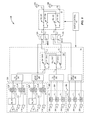
FIG. 4 is a functional schematic of radio frequency (RF) front end circuitry 26. The RF front end circuitry 26 includes a primary antenna 28A, a secondary antenna 28B, antenna swapping circuitry 30, multiplexer circuitry 32, transceiver switching circuitry 34, primary transceiver circuitry 36, secondary receiver circuitry 38, and switch control circuitry 40. The antenna swapping circuitry 30 is coupled between the multiplexer circuitry 32, the primary antenna 28A, and the secondary antenna 28B. The transceiver switching circuitry 34 is coupled between the multiplexer circuitry 32, the primary transceiver circuitry 36, and the secondary receiver circuitry 38. Each one of the antenna swapping circuitry 30 and the transceiver switching circuitry 34 are shown as a dual-pole dual-throw (DP2T) switch, however, other switch configurations may similarly be used without departing from the principles of the present disclosure. The switch control circuitry 40 is coupled to the antenna swapping circuitry 30 and the transceiver switching circuitry 34.
The multiplexer circuitry 32 includes a first multiplexer 32A and a second multiplexer 32B. Each one of the first multiplexer 32A and the second multiplexer 32B include a low-band node LB, a mid/high-band node MBHB, and a common node C, and are configured to pass low-band signals between the low-band node LB and the common node C, pass mid/high-band signals between the mid/high-band node MBHB and the common node C, and attenuate other signals.
The primary transceiver circuitry 36 includes low-band primary transceiver circuitry 36A and mid/high-band primary transceiver circuitry 36B. Similarly, the secondary receiver circuitry 38 includes low-band secondary receiver circuitry 38A and mid/high-band secondary receiver circuitry 38B. The transceiver switching circuitry 34 includes low-band primary transceiver switching circuitry 34A, mid/high-band primary transceiver switching circuitry 34B, low-band secondary receiver switching circuitry 34C, mid/high-band secondary receiver switching circuitry 34D, and low-band antenna swapping circuitry 34E. The low-band primary transceiver switching circuitry 34A is coupled between the low-band primary transceiver circuitry 36A and the low-band antenna swapping circuitry 34E. The mid/high-band primary transceiver switching circuitry 34B is coupled between the mid/high-band primary transceiver circuitry 36B and the mid/high-band node MBHB of the first multiplexer 32A. The low-band secondary receiver switching circuitry 34C is coupled between the low-band secondary receiver circuitry 38A and the low-band antenna swapping circuitry 34E. The mid/high-band secondary receiver switching circuitry 34D is coupled between the mid/high-band secondary receiver circuitry 38B and the mid/high-band node MBHB of the second multiplexer 32B. The low-band antenna swapping circuitry 34E is coupled between the low-band primary transceiver switching circuitry 34A, the low-band secondary receiver switching circuitry 34C, the low-band node LB of the first multiplexer 32A, and the low-band node LB of the second multiplexer 32B. In some configurations, the primary antenna 28A and the secondary antenna 28B may be located on opposite ends of a mobile communication device in which the RF front end circuitry 26 is used. The primary transceiver circuitry 36 may be located near the primary antenna 28A and the second transceiver circuitry 38 may be located near the secondary antenna 28B in order to reduce the distance between the components and thus improve performance. Shielded signal paths such as those provided by a coaxial cable may connect the primary transceiver circuitry 36 and the secondary transceiver circuitry 38, for example, via the transceiver switching circuitry 34. Such a configuration does not change the connections shown in FIG. 6.
The low-band antenna swapping circuitry 34E includes a first pole P1, a second pole P2, a first throw T1, a second throw T2, and a number of low-band antenna swapping switching elements SW_LBAS. The first pole P1 of the low-band antenna swapping circuitry 34E is coupled to the low-band primary transceiver switching circuitry 34A. The second pole P2 of the low-band antenna swapping circuitry 34E is coupled to the low-band secondary receiver switching circuitry 34C. The first throw T1 of the low-band antenna swapping circuitry 34E is coupled to the low-band node LB of the first multiplexer 32A. The second throw T2 of the low-band antenna swapping circuitry 34E is coupled to the low-band node LB of the second multiplexer 32B. A first low-band antenna swapping switching element SW_LBAS1 is coupled between the first pole P1 and the first throw T1. A second low-band antenna swapping switching element SW_LBAS2 is coupled between the first pole P1 and the second throw T2. A third low-band antenna swapping switching element SW_LBAS3 is coupled between the second pole P2 and the first throw T1. A fourth low-band antenna swapping switching element SW_LBAS4 is coupled between the second pole P2 and the second throw T2.
Notably, while the low-band antenna swapping circuitry 34E is shown including four low-band antenna swapping switching elements SW_LBAS arranged in a particular configuration, the present disclosure is not so limited. That is, the low-band antenna swapping circuitry 34E may include any number of switching elements arranged in any number of configurations without departing from the principles herein. Further, while the low-band antenna swapping circuitry 34E is shown separate from the other switching circuitry in the transceiver switching circuitry 34, the functionality of any of the switching circuitry in the transceiver switching circuitry 34 may be separated or combined according to well known principles. Finally, while the low-band antenna swapping circuitry 34E is shown as part of the transceiver switching circuitry 34, the low-band antenna swapping circuitry 34E may be provided independently of the transceiver switching circuitry 34 or integrated with any other portion of the RF front end circuitry 26.
The antenna swapping circuitry 30 includes a first pole P1, a second pole P2, a first throw T1, a second throw T2, and a number of antenna swapping switching elements SW_AS1-SW_AS4. A first antenna swapping switching element SW_AS1 is coupled between the first pole P1 and the first throw T1. A second antenna swapping switching element SW_AS2 is coupled between the first pole P1 and the second throw T2. A third antenna swapping switching element SW_AS3 is coupled between the second pole P2 and the first throw T1. A fourth antenna swapping switching element SW_AS4 is coupled between the second pole P2 and the second throw T2. The first pole P1 is coupled to the common node C of the first multiplexer 32A. The second pole P2 is coupled to the common node C of the second multiplexer 32B. The first throw T1 is coupled to the primary antenna 28A. The second throw T2 is coupled to the secondary antenna 28B.
While the antenna swapping circuitry 30 is shown including a specific number of antenna swapping switching elements SW_AS arranged in a particular manner, the present disclosure is not so limited. Those skilled in the art will appreciate that the principles of the present disclosure apply to antenna swapping circuitry having any number of antenna swapping switching elements SW_AS that are arranged in any manner.
The low-band primary transceiver circuitry 36A includes a number of duplexers DUP each including a transmit node T, a receive node R, and a common node C, power amplifier switching circuitry PA_SW, a power amplifier PA, and a number of low-noise amplifiers LNA. The power amplifier PA is coupled to the transmit node T of each one of the duplexers DUP via the power amplifier switching circuitry PA_SW. Each one of the low-noise amplifiers LNA is coupled to a receive node R of a different one of the duplexers DUP. Each one of the duplexers DUP is configured to pass transmit signals within one or more operating bands provided at the common node C to the transmit node T, pass receive signals within the one or more operating bands provided at the receive node R to the common node C, and attenuate other signals. A common node C of each one of the duplexers DUP is coupled to the low-band primary transceiver switching circuitry 34A.
The mid/high-band primary transceiver circuitry 36B similarly includes a number of duplexers DUP each including a transmit node T, a receive node R, and a common node C, power amplifier switching circuitry PA_SW, a power amplifier PA, and a number of low-noise amplifiers LNA. The power amplifier PA is coupled to the transmit node T of each one of the duplexers DUP via the power amplifier switching circuitry PA_SW. Each one of the low-noise amplifiers LNA is coupled to a receive node R of a different one of the duplexers DUP. Each one of the duplexers DUP is configured to pass transmit signals within one or more operating bands provided at the common node C to the transmit node T, pass receive signals within the one or more operating bands provided at the receive node R to the common node C, and attenuate other signals. A common node C of each one of the duplexers DUP is coupled to the mid/high-band primary transceiver switching circuitry 34B.
The low-band secondary receiver circuitry 38A includes a number of receiver filters FIL and a number of low-noise amplifiers LNA. Each one of the low-noise amplifiers LNA is coupled to a different one of the receiver filters FIL. Each one of the receiver filters FIL is in turn coupled to the low-band secondary receiver switching circuitry 34C. Further, each one of the filters FIL is configured to filter receive signals within one or more different operating bands.
The mid/high-band secondary receiver circuitry 38B similarly includes a number of receiver filters FIL and a number of low-noise amplifiers LNA. Each one of the low-noise amplifiers LNA is coupled to a different one of the receiver filters FIL. Each one of the receiver filters FIL is in turn coupled to the mid/high-band secondary receiver switching circuitry 34D. Further, each one of the filters FIL is configured to filter receive signals within one or more different operating bands.
As is apparent from the foregoing description of FIG. 4, the transceiver switching circuitry 34 includes low-band antenna swapping circuitry 34E that is not present in conventional RF front end circuitry. This low-band antenna swapping circuitry 34E allows for antenna swapping to be performed for low-band primary transmit signals before the multiplexer circuitry 32, which has several advantages that are discussed in detail below.
When operating the primary antenna 28A as intended, the switch control circuitry 40 configures the antenna swapping circuitry 30 and the low-band antenna swapping circuitry 34E as shown in FIG. 5. Specifically, the first low-band antenna swapping switching element SW_LBAS1 and the fourth low-band antenna swapping switching element SW_LBAS4 are closed, while the second low-band antenna swapping switching element SW_LBAS2 and the third low-band antenna swapping switching element SW_LBAS3 are open. Further, the first antenna swapping switching element SW_AS1 and the fourth antenna swapping switching element SW_AS4 are closed, while the second antenna swapping switching element SW_AS2 and the third antenna swapping switching element SW_AS3 are open. Accordingly, the low-band primary transceiver switching circuitry 34A is coupled to the low-and node LB of the first multiplexer 32A, the low-band secondary receiver switching circuitry 34C is coupled to the low-band node LB of the second multiplexer 32B, the common node C of the first multiplexer 32A is coupled to the primary antenna 28A, and the common node C of the second multiplexer 32B is coupled to the secondary antenna 28B. Primary transmit signals provided at the common node C of the first multiplexer 32A from the primary transceiver circuitry 36 are therefore provided to the primary antenna 28A, primary receive signals from the primary antenna 28A are provided to the common node C of the first multiplexer 32A and forwarded to the primary transceiver circuitry 36, and secondary receive signals from the secondary antenna 28B are provided to the common node C of the second multiplexer 32B and forwarded to the secondary receiver circuitry 38. Notably, if a low-band primary transmit signal and/or low-band primary receiver signal is not being used, the first low-band antenna swapping switch SW_LBAS1 in the low-band antenna swapping circuitry 34E may be opened to reduce loading at the first multiplexer 32A. Similarly, if a low-band secondary receiver signal is not being used, the fourth low-band antenna swapping switch SW_LBAS4 in the low-band antenna swapping circuitry 34E may be opened to reduce loading at the second multiplexer 32B.
When the primary antenna 28A and the secondary antenna 28B are switched, the configuration by the switch control circuitry 40 depends on whether a primary transmit signal is a low-band signal or a mid/high-band signal. If a primary transmit signal is a low-band signal, the switch control circuitry 40 configures the antenna swapping circuitry 30 and the low-band antenna swapping circuitry 34E as shown in FIG. 6. Specifically, the first low-band antenna swapping switching element SW_LBAS1 and the fourth low-band antenna swapping switching element SW_LBAS4 of the low-band antenna swapping circuitry 34E are open, while the second low-band antenna swapping switching element SW_LBAS2 and the third low-band antenna swapping switching element SW_LBAS3 are closed. Further, the first antenna swapping switching element SW_AS1 and the fourth antenna swapping switching element SW_AS4 of the antenna swapping circuitry 30 are closed, while the second antenna swapping switching element SW_AS2 and the third antenna swapping switching element SW_AS3 are open. Accordingly, the low-band primary transceiver switching circuitry 34A is coupled to the low-band node LB of the second multiplexer 32B, the low-band secondary receiver switching circuitry 34C is coupled to the low-band node LB of the first multiplexer 32A, the common node C of the first multiplexer 32A is coupled to the primary antenna 28A, and the common node C of the second multiplexer 32B is coupled to the secondary antenna 28B. Primary transmit signals provided at the common node C of the second multiplexer 32B from the primary transceiver circuitry 36 are therefore provided to the secondary antenna 28B, primary receive signals from the secondary antenna 28B are provided to the common node C of the second multiplexer 32B and forwarded to the primary transceiver circuitry 36, and secondary receive signals from the primary antenna 28A are provided to the common node C of the first multiplexer 32A and forwarded to the secondary receiver circuitry 38.
In short, when transmitting a low-band primary transmit signal, any antenna swapping is performed by the low-band antenna swapping circuitry 34E in the transceiver switching circuitry 34 before the multiplexer circuitry 32. The benefits to such an approach are numerous. First, since the first antenna swapping switching element SW_AS1 and the fourth antenna swapping switching element SW_AS4 are always closed in the presence of a low-band primary transmit signal and the second antenna swapping switching element SW_AS2 and the third antenna swapping switching element SW_AS3 are always open in the presence of a low-band primary transmit signal, the first antenna swapping switching element SW_AS1 and the fourth antenna swapping switching element SW_AS4 may be optimized to reduce harmonic generation in the closed state, while the second antenna swapping switching element SW_AS2 and the third antenna swapping switching element SW_AS3 may be optimized to reduce harmonic distortion in the open state. Specifically, a channel width of a number of switching devices in the first antenna swapping switching element SW_AS1 and the fourth antenna swapping switching element SW_AS4 may be increased to reduce the on-state resistance RON of the switching elements, while the number of parallel-stacked switching devices in the second antenna swapping switching element SW_AS2 and the third antenna swapping switching element SW_AS3 may be increased to reduce the off-state capacitance COFF of the switching elements. Since it is known that the first antenna swapping switching element SW_AS1 and the fourth antenna swapping switching element SW_AS4 will always be closed in the presence of a primary low-band transmit signal, these switching elements can be optimized to reduce the on-state resistance RON at the expense of the off-state capacitance COFF thereof. In other words, the off-state capacitance COFF of the first antenna swapping switching element SW_AS1 and the fourth antenna swapping switching element SW_AS4 is no longer a design factor to be concerned with. Similarly, the on-state resistance RON of the second antenna swapping switching element SW_AS2 and the third antenna swapping switching element SW_AS3 is no longer a design factor to be concerned with, and thus optimizations to the off-state capacitance COFF of these switching elements may be made at the expense of the on-state resistance RON. In some embodiments, a third harmonic distortion generated by the first antenna swapping switching element SW_AS1 and the fourth antenna swapping switching element SW_AS4 may therefore be about 6 dB to 12 dB greater in the open state than in the closed state, while a third harmonic distortion generated by the second antenna swapping switching element SW_AS2 and the third antenna swapping switching element SW_AS3 may be about 6 dB to 12 dB greater in the closed state than in the open state.
Second, since the multiplexer circuitry 32 is located between the low-band antenna swapping circuitry 34E and the antennas 28, any harmonic distortion generated by the low-band antenna swapping switching elements SW_LBAS therein is filtered by the multiplexer circuitry 32. Accordingly, the low-band antenna swapping switching elements SW_LBAS do not need to be optimized to the same degree as the antenna swapping switching elements SW_AS in the antenna swapping circuitry 30. Providing the low-band antenna swapping circuitry 34E and operating it as described above when transmitting a low-band signal may provide significant improvements in linearity due to the reduction of harmonics by the antenna swapping switching elements SW_AS in the antenna swapping circuitry 30. For example, third harmonic distortion generated by the antenna swapping switching elements SW_AS may be reduced by about 6 dB to 12 dB using the foregoing approach in some embodiments.
If a primary transmit signal is not a low-band signal, the switch control circuitry 40 configures the antenna swapping circuitry 30 and the low-band antenna swapping circuitry 34E as shown in FIG. 7. Specifically, the first low-band antenna swapping switching element SW_LBAS1 and the fourth low-band antenna swapping switching element SW_LBAS4 are closed, while the second low-band antenna swapping switching element SW_LBAS2 and the third low-band antenna swapping switching element SW_LBAS3 are open. Further, the first antenna swapping switching element SW_AS1 and the fourth antenna swapping switching element SW_AS4 are open, while the second antenna swapping switching element SW_AS2 and the third antenna swapping switching element SW_AS3 are closed. Accordingly, the low-band primary transceiver switching circuitry 34A is coupled to the low-band node LB of the first multiplexer 32A, the low-band secondary receiver switching circuitry 34C is coupled to the low-band node LB of the second multiplexer 32B, the common node C of the first multiplexer 32A is coupled to the secondary antenna 28B, and the common node C of the second multiplexer 32B is coupled to the primary antenna 28A. Primary transmit signals provided at the common node C of the first multiplexer 32A from the primary transceiver circuitry 36 are therefore provided to the secondary antenna 28B, primary receive signals from the secondary antenna 28B are provided to the common node C of the first multiplexer 32A and forwarded to the primary transceiver circuitry 36, and secondary receive signals from the primary antenna 28A are provided at the common node C of the second multiplexer 32B and forwarded to the secondary receiver circuitry 38. If a primary low-band receive signal is not being used, the first low-band antenna swapping switching element SW_LBAS1 may be opened to reduce loading at the first multiplexer 32A. Similarly, if a secondary low-band receive signal is not being used, the fourth low-band antenna swapping switching element SW_LBAS4 may be opened to reduce loading at the second multiplexer 32B.
Those skilled in the art will recognize improvements and modifications to the embodiments of the present disclosure. All such improvements and modifications are considered within the scope of the concepts disclosed herein and the claims that follow.

Claims (14)

What is claimed is:
1. Radio frequency (RF) front end circuitry comprising:
transceiver switching circuitry;
antenna swapping circuitry comprising:
a first pole and a second pole;
a first throw and a second throw; and
a first switching element coupled between the first pole and the first throw, a second switching element coupled between the first pole and the second throw, a third switching element coupled between the second pole and the first throw, and a fourth switching element coupled between the second pole and the second throw; and
multiplexer circuitry coupled between the transceiver switching circuitry and the antenna swapping circuitry; and
switch control circuitry coupled to the transceiver switching circuitry and the antenna swapping circuitry and configured to:
in a first low-band transmit mode, provide a primary low-band transmit signal at the first pole of the antenna swapping circuitry via the transceiver switching circuitry and forward the primary low-band transmit signal to the first throw via the first switching element in the antenna swapping circuitry; and
in a second low-band transmit mode, provide a primary low-band transmit signal at the second pole of the antenna swapping circuitry via the transceiver switching circuitry and forward the primary low-band transmit signal to the second throw via the fourth switching element in the antenna swapping circuitry.
2. The RF front end circuitry of claim 1 further comprising a primary antenna coupled to the first throw and a secondary antenna coupled to the second throw.
3. The RF front end circuitry of claim 1 wherein a linearity of the first switching element and the fourth switching element at low-band frequencies is greater in a closed state than in an open state, and a linearity of the second switching element and the third switching element at low-band frequencies is greater in a closed state than in an open state.
4. The RF front end circuitry of claim 3 wherein a third harmonic distortion generated by the first switching element and the fourth switching element at low-band frequencies is 6 dB to 12 dB greater in the open state than in the closed state.
5. The RF front end circuitry of claim 4 wherein a third harmonic distortion generated by the second switching element and the third switching element at low-band frequencies is 6 dB to 12 dB greater in the closed state than in the open state.
6. The RF front end circuitry of claim 5 wherein each of the first switching element, the second switching element, the third switching element, and the fourth switching element include a plurality of switching devices, each of the switching devices having a particular channel width.
7. The RF front end circuitry of claim 6 wherein the channel width of the plurality of switching devices in each of the first switching element and the fourth switching element is greater than the channel width of the plurality of switching devices in each of the second switching element and the fourth switching element.
8. The RF front end circuitry of claim 7 wherein the plurality of switching devices in each of the second switching element and the third switching element is greater than the plurality of switching devices in each of the first switching element and the fourth switching element.
9. The RF front end circuitry of claim 1 wherein the switch control circuitry is further configured to:
in a first mid/high-band transmit mode, provide a mid/high-band transmit signal at the first pole of the antenna swapping circuitry via the transceiver switching circuitry and forward the primary mid/high-band transmit signal to the first throw via the first switching element in the antenna swapping circuitry; and
in a second mid/high-band transmit mode, provide a mid/high-band transmit signal at the first pole of the antenna swapping circuitry via the transceiver switching circuitry and forward the primary mid/high-band transmit signal to the second throw via the second switching element.
10. The RF front end circuitry of claim 9 wherein a linearity of the first switching element and the fourth switching element at low-band frequencies is greater in a closed state than in an open state, and a linearity of the second switching element and the third switching element at low-band frequencies is greater in a closed state than in an open state.
11. The RF front end circuitry of claim 10 wherein a third harmonic distortion generated by the first switching element and the fourth switching element at low-band frequencies is 6 dB to 12 dB greater in the open state than in the closed state.
12. The RF front end circuitry of claim 11 wherein a third harmonic distortion generated by the second switching element and the third switching element at low-band frequencies is 6 dB to 12 dB greater in the closed state than in the open state.
13. The RF front end circuitry of claim 12 wherein a channel width of the plurality of switching devices in each of the first switching element and the fourth switching element is greater than a channel width of a plurality of switching devices in each of the second switching element and the fourth switching element.
14. The RF front end circuitry of claim 13 wherein the plurality of switching devices in each of the second switching element and the third switching element is greater than the plurality of switching devices in each of the first switching element and the fourth switching element.
US15/084,142 2015-06-17 2016-03-29 High linearity antenna swapping circuitry Active US9735850B2 (en)

Priority Applications (1)

Application Number Priority Date Filing Date Title
US15/084,142 US9735850B2 (en) 2015-06-17 2016-03-29 High linearity antenna swapping circuitry

Applications Claiming Priority (2)

Application Number Priority Date Filing Date Title
US201562180648P 2015-06-17 2015-06-17
US15/084,142 US9735850B2 (en) 2015-06-17 2016-03-29 High linearity antenna swapping circuitry

Publications (2)

Publication Number Publication Date
US20160373176A1 US20160373176A1 (en) 2016-12-22
US9735850B2 true US9735850B2 (en) 2017-08-15

Family

ID=57588624

Family Applications (1)

Application Number Title Priority Date Filing Date
US15/084,142 Active US9735850B2 (en) 2015-06-17 2016-03-29 High linearity antenna swapping circuitry

Country Status (1)

Country Link
US (1) US9735850B2 (en)

Cited By (1)

* Cited by examiner, † Cited by third party
Publication number Priority date Publication date Assignee Title
US11528010B2 (en) * 2019-01-31 2022-12-13 Murata Manufacturing Co., Ltd. Multiplexer and communication apparatus

Families Citing this family (4)

* Cited by examiner, † Cited by third party
Publication number Priority date Publication date Assignee Title
US10476534B2 (en) * 2016-12-06 2019-11-12 Qorvo Us, Inc. Multi-band radio frequency circuit
US12003974B2 (en) * 2018-07-30 2024-06-04 Qualcomm Incorporated Carrier switching and antenna switching for long term evolution and new radio dual connectivity
US20210314007A1 (en) * 2020-04-05 2021-10-07 Skyworks Solutions, Inc. Bridge combiners and filters for radio-frequency applications
CN111600616B (en) * 2020-07-10 2020-12-04 锐石创芯(深圳)科技有限公司 A radio frequency front-end architecture, antenna device and communication terminal

Citations (4)

* Cited by examiner, † Cited by third party
Publication number Priority date Publication date Assignee Title
US6560443B1 (en) * 1999-05-28 2003-05-06 Nokia Corporation Antenna sharing switching circuitry for multi-transceiver mobile terminal and method therefor
US6609010B1 (en) * 1998-11-30 2003-08-19 Sony International (Europe) Gmbh Dual frequency band transceiver
US7400862B2 (en) * 2004-10-25 2008-07-15 Skyworks Solutions, Inc. Transmit-receive switch architecture providing pre-transmit isolation
US9002282B1 (en) * 2011-12-15 2015-04-07 Marvell International Ltd. Method and apparatus for priority based coexistence arbitration

Patent Citations (4)

* Cited by examiner, † Cited by third party
Publication number Priority date Publication date Assignee Title
US6609010B1 (en) * 1998-11-30 2003-08-19 Sony International (Europe) Gmbh Dual frequency band transceiver
US6560443B1 (en) * 1999-05-28 2003-05-06 Nokia Corporation Antenna sharing switching circuitry for multi-transceiver mobile terminal and method therefor
US7400862B2 (en) * 2004-10-25 2008-07-15 Skyworks Solutions, Inc. Transmit-receive switch architecture providing pre-transmit isolation
US9002282B1 (en) * 2011-12-15 2015-04-07 Marvell International Ltd. Method and apparatus for priority based coexistence arbitration

Cited By (1)

* Cited by examiner, † Cited by third party
Publication number Priority date Publication date Assignee Title
US11528010B2 (en) * 2019-01-31 2022-12-13 Murata Manufacturing Co., Ltd. Multiplexer and communication apparatus

Also Published As

Publication number Publication date
US20160373176A1 (en) 2016-12-22

Similar Documents

Publication Publication Date Title
US10727878B2 (en) Multi-band radio frequency circuit
US9172441B2 (en) Front end circuitry for carrier aggregation configurations
US9503150B2 (en) Antenna and RF front-end arrangement
US9288031B2 (en) Switch arrangement
KR102140190B1 (en) Device including a switching unit and applications thereof
US9225382B2 (en) Tunable filter front end architecture for non-contiguous carrier aggregation
CN105049068B (en) Bypass path loss reduction
CN103155431B (en) Tunable radio front end and method
CN105827269B (en) A kind of radiofrequency signal R-T unit and electronic equipment
US10554232B2 (en) Multi-band radio frequency front-end circuit
US10084489B2 (en) Multiple antenna system and transceiver front end for interband downlink carrier aggregation
US10044375B2 (en) Multiband transmitter circuit with integrated circulators and filters
US9735850B2 (en) High linearity antenna swapping circuitry
US20120243446A1 (en) Multi-band wireless communication device with multiplexer and method of multiplexing multi-band wireless signals
US11239873B2 (en) Front-end circuit and communication device
TW201743573A (en) Mobile device
CN112769438B (en) Radio frequency MMPA device, radio frequency system and communication equipment
US20160352368A1 (en) Tunable notch filter
US20210211146A1 (en) Front end module
US20140376428A1 (en) Multi-frequency range processing for rf front end
US20180192320A1 (en) Reducing intermodulation distortion in a radio frequency circuit
US20140378075A1 (en) Multi-frequency range processing for rf front end
US10003375B2 (en) Radio frequency circuitry for carrier aggregation
KR102625588B1 (en) Antenna switch for supporting high linearity and electronic communication device including the same
CN112425082A (en) Adjustable antenna and communication terminal

Legal Events

Date Code Title Description
AS Assignment

Owner name: RF MICRO DEVICES, INC., NORTH CAROLINA

Free format text: ASSIGNMENT OF ASSIGNORS INTEREST;ASSIGNORS:KHLAT, NADIM;GRANGER-JONES, MARCUS;SIGNING DATES FROM 20160407 TO 20160411;REEL/FRAME:038267/0887

AS Assignment

Owner name: QORVO US, INC., NORTH CAROLINA

Free format text: MERGER;ASSIGNOR:RF MICRO DEVICES, INC.;REEL/FRAME:039196/0941

Effective date: 20160330

STCF Information on status: patent grant

Free format text: PATENTED CASE

MAFP Maintenance fee payment

Free format text: PAYMENT OF MAINTENANCE FEE, 4TH YEAR, LARGE ENTITY (ORIGINAL EVENT CODE: M1551); ENTITY STATUS OF PATENT OWNER: LARGE ENTITY

Year of fee payment: 4

MAFP Maintenance fee payment

Free format text: PAYMENT OF MAINTENANCE FEE, 8TH YEAR, LARGE ENTITY (ORIGINAL EVENT CODE: M1552); ENTITY STATUS OF PATENT OWNER: LARGE ENTITY

Year of fee payment: 8