US9735310B2 - Damage-and-resist-free laser patterning of dielectric films on textured silicon - Google Patents
Damage-and-resist-free laser patterning of dielectric films on textured silicon Download PDFInfo
- Publication number
- US9735310B2 US9735310B2 US15/280,247 US201615280247A US9735310B2 US 9735310 B2 US9735310 B2 US 9735310B2 US 201615280247 A US201615280247 A US 201615280247A US 9735310 B2 US9735310 B2 US 9735310B2
- Authority
- US
- United States
- Prior art keywords
- sinx
- film
- laser
- mask
- etch
- Prior art date
- Legal status (The legal status is an assumption and is not a legal conclusion. Google has not performed a legal analysis and makes no representation as to the accuracy of the status listed.)
- Expired - Fee Related
Links
Images


Classifications
-
- H—ELECTRICITY
- H10—SEMICONDUCTOR DEVICES; ELECTRIC SOLID-STATE DEVICES NOT OTHERWISE PROVIDED FOR
- H10F—INORGANIC SEMICONDUCTOR DEVICES SENSITIVE TO INFRARED RADIATION, LIGHT, ELECTROMAGNETIC RADIATION OF SHORTER WAVELENGTH OR CORPUSCULAR RADIATION
- H10F71/00—Manufacture or treatment of devices covered by this subclass
- H10F71/121—The active layers comprising only Group IV materials
-
- H01L31/1804—
-
- H01L31/02167—
-
- H01L31/022441—
-
- H01L31/028—
-
- H01L31/0682—
-
- H—ELECTRICITY
- H10—SEMICONDUCTOR DEVICES; ELECTRIC SOLID-STATE DEVICES NOT OTHERWISE PROVIDED FOR
- H10F—INORGANIC SEMICONDUCTOR DEVICES SENSITIVE TO INFRARED RADIATION, LIGHT, ELECTROMAGNETIC RADIATION OF SHORTER WAVELENGTH OR CORPUSCULAR RADIATION
- H10F10/00—Individual photovoltaic cells, e.g. solar cells
- H10F10/10—Individual photovoltaic cells, e.g. solar cells having potential barriers
- H10F10/14—Photovoltaic cells having only PN homojunction potential barriers
- H10F10/146—Back-junction photovoltaic cells, e.g. having interdigitated base-emitter regions on the back side
-
- H—ELECTRICITY
- H10—SEMICONDUCTOR DEVICES; ELECTRIC SOLID-STATE DEVICES NOT OTHERWISE PROVIDED FOR
- H10F—INORGANIC SEMICONDUCTOR DEVICES SENSITIVE TO INFRARED RADIATION, LIGHT, ELECTROMAGNETIC RADIATION OF SHORTER WAVELENGTH OR CORPUSCULAR RADIATION
- H10F77/00—Constructional details of devices covered by this subclass
- H10F77/10—Semiconductor bodies
- H10F77/12—Active materials
- H10F77/122—Active materials comprising only Group IV materials
-
- H—ELECTRICITY
- H10—SEMICONDUCTOR DEVICES; ELECTRIC SOLID-STATE DEVICES NOT OTHERWISE PROVIDED FOR
- H10F—INORGANIC SEMICONDUCTOR DEVICES SENSITIVE TO INFRARED RADIATION, LIGHT, ELECTROMAGNETIC RADIATION OF SHORTER WAVELENGTH OR CORPUSCULAR RADIATION
- H10F77/00—Constructional details of devices covered by this subclass
- H10F77/20—Electrodes
- H10F77/206—Electrodes for devices having potential barriers
- H10F77/211—Electrodes for devices having potential barriers for photovoltaic cells
- H10F77/219—Arrangements for electrodes of back-contact photovoltaic cells
-
- H—ELECTRICITY
- H10—SEMICONDUCTOR DEVICES; ELECTRIC SOLID-STATE DEVICES NOT OTHERWISE PROVIDED FOR
- H10F—INORGANIC SEMICONDUCTOR DEVICES SENSITIVE TO INFRARED RADIATION, LIGHT, ELECTROMAGNETIC RADIATION OF SHORTER WAVELENGTH OR CORPUSCULAR RADIATION
- H10F77/00—Constructional details of devices covered by this subclass
- H10F77/30—Coatings
- H10F77/306—Coatings for devices having potential barriers
- H10F77/311—Coatings for devices having potential barriers for photovoltaic cells
-
- H—ELECTRICITY
- H10—SEMICONDUCTOR DEVICES; ELECTRIC SOLID-STATE DEVICES NOT OTHERWISE PROVIDED FOR
- H10F—INORGANIC SEMICONDUCTOR DEVICES SENSITIVE TO INFRARED RADIATION, LIGHT, ELECTROMAGNETIC RADIATION OF SHORTER WAVELENGTH OR CORPUSCULAR RADIATION
- H10F77/00—Constructional details of devices covered by this subclass
- H10F77/70—Surface textures, e.g. pyramid structures
- H10F77/703—Surface textures, e.g. pyramid structures of the semiconductor bodies, e.g. textured active layers
-
- Y—GENERAL TAGGING OF NEW TECHNOLOGICAL DEVELOPMENTS; GENERAL TAGGING OF CROSS-SECTIONAL TECHNOLOGIES SPANNING OVER SEVERAL SECTIONS OF THE IPC; TECHNICAL SUBJECTS COVERED BY FORMER USPC CROSS-REFERENCE ART COLLECTIONS [XRACs] AND DIGESTS
- Y02—TECHNOLOGIES OR APPLICATIONS FOR MITIGATION OR ADAPTATION AGAINST CLIMATE CHANGE
- Y02E—REDUCTION OF GREENHOUSE GAS [GHG] EMISSIONS, RELATED TO ENERGY GENERATION, TRANSMISSION OR DISTRIBUTION
- Y02E10/00—Energy generation through renewable energy sources
- Y02E10/50—Photovoltaic [PV] energy
- Y02E10/547—Monocrystalline silicon PV cells
-
- Y—GENERAL TAGGING OF NEW TECHNOLOGICAL DEVELOPMENTS; GENERAL TAGGING OF CROSS-SECTIONAL TECHNOLOGIES SPANNING OVER SEVERAL SECTIONS OF THE IPC; TECHNICAL SUBJECTS COVERED BY FORMER USPC CROSS-REFERENCE ART COLLECTIONS [XRACs] AND DIGESTS
- Y02—TECHNOLOGIES OR APPLICATIONS FOR MITIGATION OR ADAPTATION AGAINST CLIMATE CHANGE
- Y02P—CLIMATE CHANGE MITIGATION TECHNOLOGIES IN THE PRODUCTION OR PROCESSING OF GOODS
- Y02P70/00—Climate change mitigation technologies in the production process for final industrial or consumer products
- Y02P70/50—Manufacturing or production processes characterised by the final manufactured product
Definitions
- Embodiments of the invention relate generally to the field of materials, and more particularly, to methods and systems for damage-and-resist-free laser patterning of dielectric films on textured silicon.
- PECVD Plasma Enhanced Chemical Vapor Deposition
- PECVD tools enable a process by which thin films are deposited from a gas state (vapor) to a solid state onto a substrate by chemical reactions which occur after creation of a plasma of the reacting gases.
- the plasma is generally created by RF (AC) frequency or DC discharge between two electrodes, the space between which is filled with the reacting gases.
- Dielectric films such as Silicon-Nitride and Silicon-Dioxide are used in the production of silicon solar cells. It is desirable, for the purpose of creating selective, well defined structures and metallizations to pattern these films on the surface of alkaline textured silicon.
- An industrially feasible method for patterning these films is to remove them with a laser.
- Presently known and conventional laser removal processes unfortunately causes damage to the surface of the silicon. Such processes are the best known techniques in the current state of the art and therefore, a balance is made between the extent of film removal via laser and resulting damage to the underlying silicon. For instance, greater removal of the layers exposes more silicon, and thus increases efficiency of the cell, whilst simultaneously causing increasing amounts of damage to the silicon, thus reducing efficiency of the cell.
- a lower cost laser removal process which provides sufficient layer removal and reduces damage to the underlying silicon is needed.
- FIG. 1A illustrates both direct and indirect laser removal processing schemes in accordance with the described embodiments
- FIG. 1B illustrates an alternative indirect laser removal processing scheme in accordance with the described embodiments
- FIG. 2 depicts film bandgaps in accordance with the described embodiments
- FIG. 3 depicts Scanning Electron Microscope (SEM) laser ablation images in accordance with described embodiments
- FIG. 4 depicts SEM laser ablation images from indirect laser removal processing in accordance with described embodiments
- FIG. 5 depicts camera images of plated cells
- FIG. 6 depicts SEM images of laser ablation
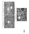
- FIG. 7 depicts SEM images of laser ablation
- FIG. 8 depicts SEM images of laser ablation
- FIG. 9 depicts SEM images with and without ghost plating
- FIG. 10 depicts a Passivated Emitter Rear Contacted (PERC) cell for which there is selected doping, contact doping, and back contacted cells; and
- PERC Passivated Emitter Rear Contacted
- FIG. 11A shows a solar cell under Illuminated Lock In Thermography (ILIT) in accordance with described embodiments
- FIG. 11B shows a solar cell under Transmission Electron Microscopy (TEM) in accordance with described embodiments
- FIG. 12 depicts Spreading Resistance Analysis (SRA) of active dopant profiles for POCl 3 emitter optimization.
- FIG. 13 is a flow diagram illustrating a method for implementing damage-and-resist-free laser patterning of dielectric films on textured silicon in accordance with described embodiments.
- Described herein are methods and systems for implementing damage-and-resist-free laser patterning of dielectric films on textured silicon.
- PECVD Plasma Enhanced Chemical Vapor Deposition
- PECVD Plasma Enhanced Chemical Vapor Deposition
- SiN x or SiO x is deposited onto c-Si.
- Dielectric films may also be thermally grown (SiO2) or deposited with techniques such as Atomic Layer Deposition (ALD), thermal evaporation, and sputtering.
- Other films include Al2O3, MgF, etc.
- a thin layer of a-Si is deposited on top of the SiN x or SiO x .
- the a-Si film is very susceptible to laser removal, but is insensitive to a Buffered Oxide Etch (BOE) (which contains hydrofluoric acid).
- BOE Buffered Oxide Etch
- the underlying SiN x or SiO x film is sensitive to BOE, but not sensitive to the laser.
- an etch mask is defined for the SiN x or SiO x which can then later be removed by a low power hydrogen plasma in the PECVD tool.
- the resultant damage free surface may then be plated with metal or exposed to other selective processes.
- Laser patterning of thin films such as SiN x , SiO x , and a-Si is desirable for solar cell production as it allows for patterning similar to what is achieved with photolithography at a fraction of the cost and may be used for processes such as contact patterning and selective doping.
- a major problem with laser ablation processes is the c-Si damage which is induced by the laser. While ‘low damage’ laser patterning is trivial on smooth surfaces, performing such patterning on surfaces textured by standard alkaline etch processes prove far more difficult and problematic.
- crystalline silicon is textured with an alkaline etch, resulting in pyramidal structures in the 1-6 micron regime.
- ⁇ 78 nm of SiN x are deposited with NH 3 and SiH 4 in a N 2 dilute plasma at ⁇ 320 degrees Celsius.
- a ⁇ 20 nm layer of a-Si is deposited with a SiH 4 in an H 2 dilute plasma at ⁇ 270 degrees Celsius.
- the resulting film stack is then used with a laser that is absorbed in the a-Si layer.
- the top layer of the film stack is ablated with a laser, in which ablating the film constitutes removal of the film from the stack.
- Both the a-Si and c-Si absorb the laser, however, the weakly bound nature of the a-Si leads to vaporization of the film before visible damage is done to the c-Si lattice.
- FIG. 1A illustrates both direct laser removal 115 and indirect laser removal 140 processing schemes in accordance with the described embodiments.
- a direct removal scheme 115 depicted on the left
- an indirect laser removal scheme 140 depicted on the right.
- Direct laser removal 115 of SiN x 105 depicted on the left details the processing scheme for direct removal of SiN x from the c-Si 110 layer at lower power conditions with an 800 nm laser causing photon vaporization of the underlying c-Si 110 .
- Vaporization of the c-Si 110 substrate can be a damage intensive process, especially with the laser intensity variation introduced with texturing processes.
- the indirect laser removal 140 process of SiN x 105 utilizes a film which can directly absorb the laser under normal conditions. It is therefore possible to remove that film without relying on vaporization of the underlying c-Si 110 substrate.
- the SiN x can be patterned with a Buffered Oxide Etch (BOE) at operation 130 owing to the chemical sensitivity of SiN x to hydrofluoric acid (HF).
- BOE Buffered Oxide Etch
- P d P avg n * t p * f , where P d is the instantaneous power density, where P avg is the measured time average power, where n is the number of triggered pulses per pulse train, where t p is the duration of the pulse, and where f is the frequency of the pulse trains from the laser system.
- the intensity variation of the laser with a textured substrate complicates the power optimization process for SiN x direct laser removal 115 and SiN x indirect laser removal 140 processes.
- For the direct laser removal 115 process an increase in the film removal is accompanied by a corresponding increase in damage. Greater film removal improves efficiency of the cell, however, the greater damage caused to the cell negates and ultimately overcomes the efficiency improvements gained. Though a balance between film removal and silicon damage may be attained, there is nevertheless a limit to the efficiency of a resulting cell due to such a tradeoff.
- undercutting e.g., chemical etching via the BOE 130 operation beneath a mask, at the perforated sites
- undercutting e.g., chemical etching via the BOE 130 operation beneath a mask, at the perforated sites
- Described in greater detail below and depicted via the following images are a series of samples, all of which are generated from p-type mono-crystalline boron doped wafers with a bulk resistivity of 1-3 ⁇ cm with a thickness of 170-200 microns.
- the substrates are pseudo square and measure 156+0.5 mm.
- Film depositions are performed with an Applied Materials Precision 5000 Plasma Enhanced Chemical Vapor Deposition (PECVD) tool.
- Laser processing of the thin films is performed with a 140 femtosecond laser with a repetition rate of 5 kHz. Each repetition of the laser generates a pulse train of approximately 6 laser pulses separated by 12.5 nanoseconds.
- Intensity control of the laser may be managed using neutral density reflective filters. When fine control is required, multiple filters are used causing pulse echoing ⁇ 1% of the transmitted power. For the processes described, such effects are purposefully neglected as the ablation process is attributed to the peak laser intensity, not the absorbed power, which remains unaffected by sub-peak intensity pulse echoing. Pulse overlap may be controlled by the scanning speed of the flying optics used to steer and focus the laser over the Si substrate.
- partial ablation is defined as the complete film removal over the defined laser spot area less than 70%. Regions covered in a thin layer of SiN x are considered as non-removed sites and are observable in the Scanning Electron Microscope (SEM) images depicted via the subsequent figures.
- SEM Scanning Electron Microscope
- Solar cells such as those depicted at FIG. 5
- elements 501 and 502 are electrical devices which convert the energy of light directly into electricity by the photovoltaic effect, which is a physical and chemical phenomenon.
- Solar or photovoltaic cells are one type of photoelectric cells representing a class of devices having electrical characteristics, such as current, voltage, or resistance, that vary when exposed to light.
- Such solar or photovoltaic cells are the building blocks of photovoltaic modules, otherwise known as solar panels which are revolutionizing the energy market today.
- PV photovoltaic
- contacts on the front of a solar cell there are contacts on the front of a solar cell and these contacts are made of metal. Because the metal contacts themselves are not transparent to light, any light that hits the metal contacts is not absorbed by the solar cell as it is reflected away. In such a way, the contacts reduce the amount of power that the solar cell potentially could have generated if not for the light hitting these metal contacts.
- the conventional metal contacts are reduced in size to make finer metal contacts which in turn overcomes some of the resistance to light absorption and increases the amount of light energy received by the photovoltaic cells by decreasing the amount of light blocked by such contacts.
- the leading technology by which the metallic contacts are formed is through a process called screen printing, in which there is a metal mesh screen through which paste is pushed to assume the shape of the emulsion on the metal mesh screen.
- screen printing in which there is a metal mesh screen through which paste is pushed to assume the shape of the emulsion on the metal mesh screen.
- practice of the disclosed embodiments permits the creation of metal contacts of significantly smaller size, reduced from the present 80 to 100 microns range to less than 20 microns reliably.
- Such a size represents a significant improvement in light absorption over present technologies and is reaching the point where smaller contacts yield negligible improvement due to the diminishing returns alluded to above.
- a 10 micron contact may be negligibly better in terms of efficiency, the gains are insignificant compared to the improvement gains achieved by reducing the metal contact size from the present 80 to 100 microns range to less than 20 microns.
- prior solutions involve the removal of a non-conductive film from a surface with an ultraviolet (UV), very short, pico-second pulsed laser.
- UV ultraviolet
- Such a laser removes silicon nitride though a thermal process. More particularly, the energy absorbed in the silicon nitride non-conductive film produces just so much heat that the film is removed in that area.
- Silicon nitride non-conductive film has a melting temperature of over 2,000 degrees C. and is layered on top of a silicon material which has a melting temperature of just over 1400 degrees.
- Solar cells are intentionally rough with an intentionally design induced alkaline texture which increases their efficiency and thus provides an appreciable increase in output current. If the surface is polished or melted smooth then the surface becomes increasingly reflective and simply reflects a greater portion of the light energy received rather than absorbing the light to produce electricity.
- defects manifest themselves as either point defects, threading defects into the silicon, or trench defects observable within the silicon.
- one type of defect causes ridging all the way up the pyramidal structures formed by the intentionally design induced alkaline texture, in which the ridging occurs at the wavelength of the laser that utilized with the depth of the defect being a function of the wavelength in addition to a function of the intensity of the laser light.
- Such a cell as two main regions, a first region of a material that prefers the absence of an electron, a hole, and then also a very thin top surface of a material made to prefer electrons.
- the first region which prefers the absence of an electron usually varies between, approximately 400 nanometers and 1,000 nanometers in thickness.
- the second region which prefers the presence of an electron and which forms the top surface must be protected as any damage makes it less efficient as it is more difficult for the current to reach the contacts and thus reduces electrical power output.
- the sacrificial layer may be the a-Si 125 thin film layer as depicted at FIG. 1 , however, the sacrificial layer may be other materials which are sensitive to a removal process.
- the a-Si 125 thin film is sensitive to laser removal whereas the other film, the silicon nitride SiNx 105 is a non-conductive film which is not sensitive to the laser removal.
- the top sacrificial layer is patterned at the top surface to expose the substrate of the potential solar cell. In so doing, the pattern induced into the top film is then set into the bottom film.
- the sacrificial a-Si 125 layer is placed upon the substrate via a screen printing process which is then lithographically exposed to light.
- the sacrificial a-Si 125 layer is printed upon the substrate and then patterned with a laser.
- the printing operation introduces yet another operation in to the process and may therefore represent a less preferred method.
- both the SiNx 105 layer and the a-Si 125 sacrificial layer are placed in the same step or operation by changing gas flows during the operation.
- the gases utilized by the tool to place the layers are available whether or not they are typically utilized for the process.
- a tool capable of placing down silicon nitride can also place down the a-Si sacrificial layer through a change in gas flows and can place the a-Si sacrificial thin film on top of the silicon nitride layer during the same operation simply by changing the gas flows.
- FIG. 1B illustrates an alternative indirect laser removal 141 processing scheme in accordance with the described embodiments.
- a low level plasma etch is not utilized.
- operation 135 depicting the H2 plasma from FIG. 1A is replaced with a different operation at FIG. 1B .
- alternative processing for indirect laser removal 414 of silicon nitride with the laser process begins with depositing the amorphous silicon (a-Si) 125 mass on top of the Silicon Nitride (SiNx) 125 and at operation 120 laser patterning creates the desired mask.
- a-Si amorphous silicon
- SiNx Silicon Nitride
- the patterned solar cell under manufacture is then exposed to a buffered oxide etch (BOE) at operation 120 which takes the laser patterned mask from the amorphous silicon (a-Si) 125 and sets it into the silicon nitride (SiNx) 105 , however, rather than utilizing the hydrogen plasma at operation 135 from FIG. 1A , the operation is replaced with a dilute Potassium Hydroxide (KOH) operation 136 as depicted at FIG. 1B .
- BOE buffered oxide etch
- the low level plasma etch operation of FIG. 1A accelerates protons at the surface with a reactive ion etch tool, however, certain manufacturing facilities may not have such a reactive ion etch tool and therefore, the dilute Potassium Hydroxide (KOH) operation 136 may be preferred for certain implementations to attain the same result.
- KOH Potassium Hydroxide
- both the dilute KOH 136 of FIG. 1B and the hydrogen plasma etch operation at element 135 of FIG. 1A work effectively well.
- FIG. 2 depicts film bandgaps in accordance with the described embodiments.
- the crosshatched region indicates where both the film and c-Si exhibit direct absorption of the femto-second laser.
- the a-Si sacrificial layer is an amorphous silicon differentiated from the silicon nitride as the amorphous silicon a-Si sacrificial layer is void or substantially void of measurable quantities of nitrogen.
- the amorphous silicon a-Si sacrificial layer presents optical characteristics which are different from the underlying silicon nitride layer which can be exploited. More particularly, the amorphous silicon a-Si sacrificial layer absorbs light more strongly than the silicon nitride.
- the Tuac Plot 201 of PECVD SiNx and a-Si Versus Laser Energy is also called a Lorenz plot and the plot having both of the different films demonstrates the optical absorption characteristics of the two different films, both the silicon nitride layer and the amorphous silicon a-Si sacrificial layer.
- silicon nitride 205 plot there is observable a very wide-bandgap material meaning that it does not absorb light very well, which is beneficial as the layer is being placed at a top surface of a solar cell where the intention is for the solar cell to absorb the light and not the film on top.
- silicon nitride because of the wide-bandgap film, the silicon nitride also does not absorb the laser energy well either and consequently, patterning the silicon nitride is very challenging.
- an ultraviolet laser is utilized for the patterning process because the ultraviolet light is absorbed by the silicon nitride.
- the amorphous silicon making up the sacrificial layer exhibits a much smaller bandgap which may be tailored all the way down to approximately 1.3 or 1.4 electron volts. Consequently, the film will very strongly absorb the laser light and because the laser light is absorbed more readily the film is significantly easier to remove.
- the potential solar cell being manufactured is then placed into a hydrofluoric acid with a buffer chemical.
- the buffer chemical is utilized to make the process stable over time, however the hydrofluoric acid actually causes the removal of the hue.
- the amorphous silicon does not etch in hydrofluoric acid however, the silicon nitride SiNx layer does etch, and therefore, depending on the manner by which the silicon nitride is deposited, the SiNx layer will either etch very quickly or very slowly or moderately quickly.
- the silicon nitride SiNx layer is deposited via plasma-enhanced chemical vapor deposition, PECVD, process which enables the SiNX to be easily removed with the hydrofluoric acid prior to any high temperature processes.
- PECVD plasma-enhanced chemical vapor deposition
- the solar cell being manufactured is exposed to a 10:1 buffered oxide etch which contains hydrofluoric acid for 5 minutes to remove the silicon nitride where it caused damage to the amorphous silicon leaving behind a non-ideal amorphous silicon layer on top of the silicon nitride layer which will absorb light and decrease the efficiency of the solar cells.
- a 10:1 buffered oxide etch which contains hydrofluoric acid for 5 minutes to remove the silicon nitride where it caused damage to the amorphous silicon leaving behind a non-ideal amorphous silicon layer on top of the silicon nitride layer which will absorb light and decrease the efficiency of the solar cells.
- the substrate is then returned to the PECVD tool, however, rather than running a depositing plasma or plasma that deposits material, an etching plasma operation is run using a relatively low power hydrogen plasma.
- This etching plasma operation removes the amorphous silicon because the amorphous silicon already has a significant quantity of hydrogen within it and therefore, by hitting the amorphous silicon layer with hydrogen atoms via the etching plasma, the remaining amorphous silicon is removed as it reverts back to the silane SiH4 gas originally utilized to deposit the film.
- the molecular bonds of silicon nitrogen are significantly stronger than the bonds of silicon hydrogen and consequently, the silicon nitride film does not change in thickness via this process and it would be very difficult to remove the silicon nitride film with hydrogen plasma etch due to the high preference whereas removal of the amorphous silicon film is very easy to remove via the hydrogen plasma etch (e.g., as depicted at FIG. 1 , element 135 ).
- the crystalline silicon with the patterned silicon nitride remains behind with nothing else, thus leaving the desired patterned silicon nitride film.
- a light-induced plating process is then utilized to deposit the metal contacts and because there is no damage or only minimal damage to the crystalline silicon a much higher efficiency solar cell with very small metal contacts defined with laser is provided.
- the 1.2 shots (SEM image 303 ) and 1.3 shots (SEM image 302 ) indicate a 20% and 30% spot overlap, respectively.
- the 5 shots (element 301 ) indicate that each location in the laser line was exposed to 5 shots from the laser. Overlaps of 20 and 30% are used in order to achieve a consistent line.
- Elements 301 and 302 demonstrate a direct removal of the SiN x film. Peeling at the edge of the lasing site indicates that the film is lifted off from the underlying c-Si from c-Si vaporization.
- the cone or pyramid shape is very pitted and ragged, which reduces efficiency of the resulting solar cell.
- Amorphous silicon is a poor conductor but it does conduct electrons.
- silicon nitride is an extremely poor conductor. As can be seen here at element 402 the amorphous silicon has been mostly removed and the surfaced is no longer visible. When the solar cell being manufactured is then placed into the hydrofluoric acid the silicon nitride is removed. After removal of the silicon nitride it is then possible to see the surface again, thus exposing the alkaline texturing and resulting in greater film removal with significantly less damage to the silicon substrate.
- HF may thus be utilized to selectively remove the SiN x where the a-Si has been ablated. If the a-Si is incompletely ablated, then etch time is extended to undercut the residual film and fully open the contact without visible surface defects.
- the film stack now demonstrates charging, when imaged with SEM, where the laser has removed the top layer of the film.
- the substrate c-Si with its film stacks
- BOE comprised of, by way of example, NH 4 F and HF for 7 minutes in accordance with a particular embodiment.
- SiO x functions as the film to be removed.
- Alternative etch processes may likewise be utilized to optimize the etch as well.
- Such a chemical etch results in the removal of SiNx (or SiO x ) only where the a-Si has been removed by the laser.
- the a-Si film is then removed with a low power H 2 plasma etch in the PECVD tool.
- the H 2 plasma etch does not etch the SiN x or SiOx films, resulting in a fully patterned dielectric film with no absorbing a-Si layer.
- the patterning depicted at SEM images 301 - 304 at FIG. 3 from direct ablation of SiN x without the chemical masking as depicted at SEM images 401 and 402 results in either incomplete ablation such as that which is depicted by SEM image 301 at FIG.
- SEM image 401 demonstrates the charging of the local opening in the a-Si film from the laser ablation of the film.
- the charging is indicative of a non-conductive film and is the result of exposure of the underlying SiN x film.
- SEM image 402 contains a much clearer image, as the SiN x film has been locally removed with BOE.
- the a-Si film is then removed with a low power hydrogen plasma, leaving the SiN x intact.
- the 5 nm a-Si mask does not prove to be robust enough for fully blocking HF across the substrate, and causes the formation of pinholes in the SiN x film.
- Pinholes coupled with Light-Induced-Plating (LIP) lead to ghost plating which is the deposition and growth of metal in non-contact locations.
- ghost plating reduces finger conductivity, causes pattern loss, and shades the cell, all of which are undesirable and degrades efficiency and power generation of the resulting cell.
- FIG. 5 depicts camera images of plated cells. Specifically depicted are a camera image 501 of a plated cell with a 5 nm a-Si etch mask and camera image 502 of a plated cell with a 20 nm a-Si etch mask in accordance with described embodiments.
- the cells pictured at camera images 501 and 502 were formed using the indirect laser removal process 101 as depicted at FIG. 1 , followed by LIP Ni and Cu on c-Si(p) bulk cells with a bulk resistivity of 1-3 ohm-cm and an n-type emitter with a sheet resistance of 60 ohms/square.
- the cell pictured at camera image 501 has substantial ghost plating and pattern loss whereas the cell pictured at camera image 502 does not.
- the increase in the a-Si mask thickness decreases the non-contact area plating, but it also makes laser removal of the a-Si more challenging with the same laser intensity.
- FIG. 6 depicts SEM images of laser ablation. Specifically depicted are SEM image 601 of a laser ablation line with 20 nm a-Si etch mask after BOE etch and SEM image 602 of a laser ablation line with 40 nm a-Si etch mask after BOE in accordance with described embodiments.
- SEM image 601 of a laser ablation line with 20 nm a-Si etch mask after BOE etch SEM image 602 of a laser ablation line with 40 nm a-Si etch mask after BOE in accordance with described embodiments.
- SEM images 701 and 702 A and 702 B share the same BOE etch time and demonstrated that an increase in laser intensity increases the local opening in the SiN x for a fixed BOE etch time.
- close inspection SEM images 702 A and 702 B show the emergence of small visible laser induced defects (LID) at the peaks of the pyramids as indicated by the red circles in SEM image 702 A.
- the white lines bounding the defect in SEM image 702 B shows the defect is ⁇ 200 nm in diameter, a quarter the wavelength of the laser.
- SEM image 701 with its 20 nm mask has substantially less film residue after the BOE process compared to the 40 nm mask in SEM image 602 at FIG. 6 .
- the increase in mask thickness will completely obscure the contact region for plating, and prevent proper contact to the emitter (the top layer of the c-Si solar cell).
- a-Si layer acts as a shield for the c-Si and sufficiently absorbs the laser to prevent damage of the underlying substrate, then higher laser powers may be utilized to process and remove the residual film without causing damage.
- SEM images 801 and 802 show the defects generated at this intersection resultant from pulse overlap. Such behavior is similar to the defect generation observed at SEM image 301 of FIG. 3 for smooth surfaces.
- the white lines in SEM image 801 show the approximate size of the defects to again be ⁇ 200 nm.
- the laser pulse exposure overlaps with a previous laser pulse exposure there is a double pulse of intensity resulting in the small pit holes. Because the laser applied is a pulsed laser, at a given frequency, there is a short but more intense and localized burst of energy.
- the amorphous silicon layer As a sacrificial layer, the amorphous silicon is effectively silicon, however, because it is weakly bound silicon, the amount of energy needed to get an electron to break a bond is much lower.
- these energetic electrons are generated which break the bonds to create a plasma resulting in plasma ablation without damaging the pristine crystalline silicon structure which must remain for optimal solar cell operational efficiency.
- FIG. 9 depicts SEM images with and without ghost plating. Specifically depicted are SEM image 901 of a finger without ghost plating, SEM image 902 of a finger/busbar intersection without ghost plating, SEM image 903 of a finger with ghost plating, and SEM image 904 of a finger/busbar intersection with ghost plating.
- SEM images 901 and 902 show the formation of 20-25 micron micro-wires with an 8-12 micron SiN x opening without the presence of ghost plating.
- SEM images 903 and 904 show the presence of ghost plating and the effect it has on finger formation.
- the spacing between the wires in SEM images 902 and 904 that comprise the busbar reduces the film stress in the busbar and improves metal adhesion. Samples without this spacing would experience peeling at the busbar after a 5 minute 350° C. anneal, samples with adequate spacing to prevent wire-merging did not have this issue.
- Enhancing the absorption of the laser in the a-Si may further decrease the power required for film ablation, reduction in c-Si damage, and minimize residual film at the contact location. Furthermore, a lighter doped n-region may improve passivation of the emitter.
- FIG. 10 depicts a depicts a Passivated Emitter Rear Contacted (PERC) cell 1001 for which there is selected doping, contact doping, and back contacted cells.
- PERC Passivated Emitter Rear Contacted
- FIG. 10 depicts a depicts a Passivated Emitter Rear Contacted (PERC) cell 1001 for which there is selected doping, contact doping, and back contacted cells.
- a solar cell resulting from the above described processes may be observed, in which there is a bottom AI base layer 1045 upon which a c-Si (p-type) substrate layer 1020 is provided, over which a SiO 2 layer 1050 is depicted and finally at the top surface a SiN x layer 1005 is provided.
- FIG. 11A shows a solar cell under Illuminated Lock In Thermography (ILIT) in accordance with described embodiments.
- ILIT Illuminated Lock In Thermography
- the small defects 1105 observed the ILIT image 1101 are a likely source of shunting. Conversely, the lack of bright spots in ILIT image 1102 indicates that removing the busbar—and laser line intersections with it—eliminates the shunts in the cell which will therefore result in a more efficient solar cell as captured energy is converted to electrical output rather than converted to wasteful heat due to the shunts.
- the small laser induced defects exhibit a relatively low defect density. Ideally any defects which due occur are shallow enough that they won't perforate the emitter of a silicon solar cell under manufacture as it will reduce the operational efficiency of the same solar cell once in operation. Any apparent shunting as a result of defects 1105 appear as a bright spot from localized heating.
- the bight spots identified at element 1101 as defects 1105 are thus a likely source of shunting.
- FIG. 11B shows a solar cell under Transmission Electron Microscopy (TEM) in accordance with described embodiments. Specifically depicted is a cross sectional TEM image of laser line intersection with Laser Induced Damage or “LIDs.”
- TEM Transmission Electron Microscopy
- a TEM image at a scale of 2 microns showing pyramid peak, sidewall, and trough damage On the top right at element 1121 is a TEM image at a scale of 0.5 microns showing pyramid trough damage with a depth of 500 nanometers.
- a TEM image of pyramid peak damage with a depth of 40 nm On the bottom right at element 1123 is a TEM image at a scale of 200 nanometers showing a pyramid sidewall defect.
- Investigation utilizing the TEM imagery of the busbar/finger intersection indicates the source of the shunting defects 1105 observed in FIG. 11A at element 1101 .
- There are a series of varied defects in as depicted at FIG. 11B most of which are approximately ⁇ 40 nm deep.
- the random nature of the size and distribution of the pyramids occasionally causes an interaction with the laser (constructive interference) with a sufficient intensity to form a deeper defect thus resulting n the shunt defects 1105 depicted and causing a reduce efficiency of the solar cell due to the defects resulting in heating rather than conversion to electrical output.
- silicon nitride SiNx
- silicon oxide SiOx
- hydrogenated amorphous silicon a-Si:H
- Photolithography is a well-developed standard in integrated chip manufacturing, however, can be expensive for implementation in industrial production of solar cells.
- Laser patterning provides a cheaper alternative to photolithography, but conventionally would create defects in textured surfaces.
- LID defects attributable to the intersection of the laser patterning and the busbar are removed entirely by creating an effective busbar with an alternative technology, such as press on tin coated-copper wires.
- a shunt defect is the result when the front side of the solar cell contacts the back side of the solar cell. More specifically, the defect is a result of shunting the solar cell emitter which causes a drop in cell performance because the shunt resistance drops which results in hot spots due to the conversion of energy to heat rather than electrical output.
- the busbar is not patterned by the laser thus avoiding the laser line intersection with the busbar which result in the LID defects.
- the laser patterning of the solar cell is conducted without patterning the busbar and the busbar is therefore put down via a different method, such as via the replacing of the busbar with press on tin coated copper wires.
- FIG. 12 depicts Spreading Resistance Analysis (SRA) 1201 of active dopant profiles for POCl 3 emitter optimization.
- SRA Spreading Resistance Analysis
- polished p-type silicon wafers were processed and analyzed with SRA resulting in the SRA analysis shown here having profiles resulting from the varied O2/N2 carrier gas ratio 1205 with concentration (cm ⁇ 3 ) on the vertical axis and depth in microns ( ⁇ m) on the horizontal axis.
- the finger/busbar intersection resulted in defects that fully perforated all of the emitters depicted via the SRA 1201 profile.
- Removal of the busbar pattern from the solar cell under manufacture solves this problem and then the adoption of a multi-wire approach to make contact with the fingers of the solar cell provides the necessary electrical connectivity.
- the multi-wire solution (eliminating the patterning of the busbar) offers several advantages over a busbar design including the elimination of contact resistance and shunt resistance of the resulting solar cell which therefore will exhibit greater efficiencies in terms of increased electrical output.
- the defect goes 500 nanometers deep, from the first dotted line the depth of the defect can be seen to be approximately 0.2 microns.
- the next line to the right shows a defect with a depth of approximately 0.3 microns.
- the next depth is shown at approximately 0.4 microns and the last is shown with a depth of approximately 0.44 microns.
- the 500 nanometer deep defect goes through every single one of these meaning that a front region of the solar cell will be shorted to the back region by the metal contacts deposited on the surface, thus negatively affecting performance of the solar cell manufactured.
- FIG. 13 is a flow diagram 1300 illustrating a method for implementing damage-and-resist-free laser patterning of dielectric films on textured silicon in accordance with described embodiments.
- Some of the blocks and/or operations listed below are optional in accordance with certain embodiments. The numbering of the blocks presented is for the sake of clarity and is not intended to prescribe an order of operations in which the various blocks must occur. Additionally, operations from flow 1300 may be utilized in a variety of combinations.
- Method 1300 begins at block 1305 where the method includes depositing a Silicon nitride (SiNx) or SiOx (silicon oxide) layer onto a crystalline silicon (c-Si) substrate by a Plasma Enhanced Chemical Vapor Deposition (PECVD) processing.
- SiNx Silicon nitride
- SiOx silicon oxide
- PECVD Plasma Enhanced Chemical Vapor Deposition
- processing includes depositing an amorphous silicon (a-Si) film on top of the SiNx or SiOx layer.
- a-Si amorphous silicon
- processing includes patterning the a-Si film to define an etch mask for the SiNx or SiOx layer.
- processing includes removing the SiNx or SiOx layer via a Buffered Oxide Etch (BOE) chemical etch to expose the c-Si surface.
- BOE Buffered Oxide Etch
- processing includes removing the a-Si mask with a hydrogen plasma etch in a PECVD tool to prevent current loss from the mask.
- processing includes plating the exposed c-Si surface with metal contacts.
- depositing a thin layer of a-Si on top of the SiN x or SiO x prepares the film for metallization without damaging the underlying c-Si.
- the a-Si film is susceptible to laser removal, but is insensitive to the BOE chemical etch.
- the underlying SiN x or SiO x film is sensitive to BOE chemical etch, but not sensitive to the laser.
- removing the SiN x or SiO x layer via a low power hydrogen plasma in a PECVD tool comprises exposing the c-Si surface to expose a damage free c-Si surface.
- method 1300 further includes exposing the exposed damage free c-Si surface to other selective processing before plating with metal.
Landscapes
- Life Sciences & Earth Sciences (AREA)
- Engineering & Computer Science (AREA)
- Sustainable Development (AREA)
- Sustainable Energy (AREA)
- Drying Of Semiconductors (AREA)
- Photovoltaic Devices (AREA)
Abstract
Description
where Pd is the instantaneous power density, where Pavg is the measured time average power, where n is the number of triggered pulses per pulse train, where tp is the duration of the pulse, and where f is the frequency of the pulse trains from the laser system.
Claims (19)
Priority Applications (1)
| Application Number | Priority Date | Filing Date | Title |
|---|---|---|---|
| US15/280,247 US9735310B2 (en) | 2015-10-21 | 2016-09-29 | Damage-and-resist-free laser patterning of dielectric films on textured silicon |
Applications Claiming Priority (3)
| Application Number | Priority Date | Filing Date | Title |
|---|---|---|---|
| US201562244516P | 2015-10-21 | 2015-10-21 | |
| US201662286914P | 2016-01-25 | 2016-01-25 | |
| US15/280,247 US9735310B2 (en) | 2015-10-21 | 2016-09-29 | Damage-and-resist-free laser patterning of dielectric films on textured silicon |
Publications (2)
| Publication Number | Publication Date |
|---|---|
| US20170117432A1 US20170117432A1 (en) | 2017-04-27 |
| US9735310B2 true US9735310B2 (en) | 2017-08-15 |
Family
ID=58559065
Family Applications (1)
| Application Number | Title | Priority Date | Filing Date |
|---|---|---|---|
| US15/280,247 Expired - Fee Related US9735310B2 (en) | 2015-10-21 | 2016-09-29 | Damage-and-resist-free laser patterning of dielectric films on textured silicon |
Country Status (1)
| Country | Link |
|---|---|
| US (1) | US9735310B2 (en) |
Cited By (1)
| Publication number | Priority date | Publication date | Assignee | Title |
|---|---|---|---|---|
| EP4475196A1 (en) * | 2023-06-08 | 2024-12-11 | Zhejiang Jinko Solar Co., Ltd. | Solar cell and method for producing the same |
Families Citing this family (7)
| Publication number | Priority date | Publication date | Assignee | Title |
|---|---|---|---|---|
| KR101998743B1 (en) * | 2017-06-14 | 2019-07-10 | 엘지전자 주식회사 | Compound semiconductor solar cell and method of manufacturing the same |
| KR20180138267A (en) | 2017-06-20 | 2018-12-31 | 삼성디스플레이 주식회사 | Condensed cyclic compound and organic light emitting device comprising the same |
| CN110634999A (en) * | 2018-06-21 | 2019-12-31 | 君泰创新(北京)科技有限公司 | Solar cell and manufacturing method thereof |
| JP7202396B2 (en) * | 2018-12-26 | 2023-01-11 | 株式会社カネカ | SOLAR CELL MANUFACTURING METHOD AND SOLAR CELL MANUFACTURING APPARATUS |
| US11393938B2 (en) | 2019-04-02 | 2022-07-19 | Utica Leaseco, Llc | Laser-textured thin-film semiconductors by melting and ablation |
| CN109935640B (en) * | 2019-04-02 | 2021-11-05 | 江苏微导纳米科技股份有限公司 | A kind of coating method of crystalline silicon solar cell |
| CN117285002B (en) * | 2023-11-23 | 2024-02-23 | 华东理工大学 | Method for rapidly manufacturing silicon micro-channel by laser induction and wet etching |
Citations (6)
| Publication number | Priority date | Publication date | Assignee | Title |
|---|---|---|---|---|
| US4992847A (en) * | 1988-06-06 | 1991-02-12 | Regents Of The University Of California | Thin-film chip-to-substrate interconnect and methods for making same |
| US5011567A (en) * | 1989-12-06 | 1991-04-30 | Mobil Solar Energy Corporation | Method of fabricating solar cells |
| US5017509A (en) * | 1988-07-19 | 1991-05-21 | Regents Of The University Of California | Stand-off transmission lines and method for making same |
| US20090239331A1 (en) * | 2008-03-24 | 2009-09-24 | Palo Alto Research Center Incorporated | Methods for forming multiple-layer electrode structures for silicon photovoltaic cells |
| US20140370650A1 (en) * | 2012-11-05 | 2014-12-18 | Solexel, Inc. | Monolithically isled back contact back junction solar cells using bulk wafers |
| US20160126369A1 (en) * | 2014-11-04 | 2016-05-05 | Atomic-Energy Council-Institute Of Nuclear Engergy Research | Semiconductor device and patterning method for plated electrode thereof |
-
2016
- 2016-09-29 US US15/280,247 patent/US9735310B2/en not_active Expired - Fee Related
Patent Citations (6)
| Publication number | Priority date | Publication date | Assignee | Title |
|---|---|---|---|---|
| US4992847A (en) * | 1988-06-06 | 1991-02-12 | Regents Of The University Of California | Thin-film chip-to-substrate interconnect and methods for making same |
| US5017509A (en) * | 1988-07-19 | 1991-05-21 | Regents Of The University Of California | Stand-off transmission lines and method for making same |
| US5011567A (en) * | 1989-12-06 | 1991-04-30 | Mobil Solar Energy Corporation | Method of fabricating solar cells |
| US20090239331A1 (en) * | 2008-03-24 | 2009-09-24 | Palo Alto Research Center Incorporated | Methods for forming multiple-layer electrode structures for silicon photovoltaic cells |
| US20140370650A1 (en) * | 2012-11-05 | 2014-12-18 | Solexel, Inc. | Monolithically isled back contact back junction solar cells using bulk wafers |
| US20160126369A1 (en) * | 2014-11-04 | 2016-05-05 | Atomic-Energy Council-Institute Of Nuclear Engergy Research | Semiconductor device and patterning method for plated electrode thereof |
Cited By (4)
| Publication number | Priority date | Publication date | Assignee | Title |
|---|---|---|---|---|
| EP4475196A1 (en) * | 2023-06-08 | 2024-12-11 | Zhejiang Jinko Solar Co., Ltd. | Solar cell and method for producing the same |
| NL2035738A (en) * | 2023-06-08 | 2024-12-17 | Jinko Solar Co Ltd | Solar cell and method for producing the same |
| US12278302B2 (en) | 2023-06-08 | 2025-04-15 | Zhejiang Jinko Solar Co., Ltd. | Solar cell and method for producing the same |
| US12283642B2 (en) | 2023-06-08 | 2025-04-22 | Zhejiang Jinko Solar Co., Ltd. | Solar cell and method for producing the same |
Also Published As
| Publication number | Publication date |
|---|---|
| US20170117432A1 (en) | 2017-04-27 |
Similar Documents
| Publication | Publication Date | Title |
|---|---|---|
| US9735310B2 (en) | Damage-and-resist-free laser patterning of dielectric films on textured silicon | |
| Röder et al. | Add‐on laser tailored selective emitter solar cells | |
| US8637340B2 (en) | Patterning of silicon oxide layers using pulsed laser ablation | |
| US9768343B2 (en) | Damage free laser patterning of transparent layers for forming doped regions on a solar cell substrate | |
| US9455362B2 (en) | Laser irradiation aluminum doping for monocrystalline silicon substrates | |
| TWI845484B (en) | Interdigitated back-contacted solar cell with p-type conductivity and manufacturing thereof and photovoltaic module | |
| US9508886B2 (en) | Method for making a crystalline silicon solar cell substrate utilizing flat top laser beam | |
| US20120225515A1 (en) | Laser doping techniques for high-efficiency crystalline semiconductor solar cells | |
| US20130130430A1 (en) | Spatially selective laser annealing applications in high-efficiency solar cells | |
| US20150017747A1 (en) | Method for forming a solar cell with a selective emitter | |
| US20130164883A1 (en) | Laser annealing applications in high-efficiency solar cells | |
| KR101384853B1 (en) | Laser processing methods for photovoltaic solar cells | |
| KR101457427B1 (en) | Solar cells and methods of fabrication thereof | |
| US9214585B2 (en) | Annealing for damage free laser processing for high efficiency solar cells | |
| US20130199606A1 (en) | Methods of manufacturing back surface field and metallized contacts on a solar cell device | |
| US20170005206A1 (en) | Patterning of silicon oxide layers using pulsed laser ablation | |
| Hsiao et al. | 266-nm ps laser ablation for copper-plated p-type selective emitter PERC silicon solar cells | |
| Fırat et al. | Industrial metallization of fired passivating contacts for n-type tunnel oxide passivated contact (n-TOPCon) solar cells | |
| Wang et al. | Silicon solar cells based on all‐laser‐transferred contacts | |
| EP2819181A1 (en) | Laser annealing applications in high-efficiency solar cells | |
| CN102498577A (en) | Threshold adjustment implants for reducing surface recombination in solar cells | |
| WO2014179366A1 (en) | Annealing for damage free laser processing for high efficiency solar cells | |
| KR20130007582A (en) | A method for forming a selective contact | |
| KR101954436B1 (en) | Method for forming metal silicide layers | |
| KR20140008533A (en) | Spatially selective laser annealing applications in high-efficiency solar cells |
Legal Events
| Date | Code | Title | Description |
|---|---|---|---|
| AS | Assignment |
Owner name: ARIZONA BOARD OF REGENTS ON BEHALF OF ARIZONA STAT Free format text: ASSIGNMENT OF ASSIGNORS INTEREST;ASSIGNOR:BAILLY, MARK SCOTT;REEL/FRAME:039898/0322 Effective date: 20160922 |
|
| AS | Assignment |
Owner name: NATIONAL SCIENCE FOUNDATION, VIRGINIA Free format text: CONFIRMATORY LICENSE;ASSIGNOR:ARIZONA STATE UNIVERSITY, TEMPE;REEL/FRAME:040315/0809 Effective date: 20161011 |
|
| STCF | Information on status: patent grant |
Free format text: PATENTED CASE |
|
| MAFP | Maintenance fee payment |
Free format text: PAYMENT OF MAINTENANCE FEE, 4TH YEAR, MICRO ENTITY (ORIGINAL EVENT CODE: M3551); ENTITY STATUS OF PATENT OWNER: MICROENTITY Year of fee payment: 4 |
|
| FEPP | Fee payment procedure |
Free format text: MAINTENANCE FEE REMINDER MAILED (ORIGINAL EVENT CODE: REM.); ENTITY STATUS OF PATENT OWNER: MICROENTITY |
|
| LAPS | Lapse for failure to pay maintenance fees |
Free format text: PATENT EXPIRED FOR FAILURE TO PAY MAINTENANCE FEES (ORIGINAL EVENT CODE: EXP.); ENTITY STATUS OF PATENT OWNER: MICROENTITY |
|
| STCH | Information on status: patent discontinuation |
Free format text: PATENT EXPIRED DUE TO NONPAYMENT OF MAINTENANCE FEES UNDER 37 CFR 1.362 |
|
| FP | Lapsed due to failure to pay maintenance fee |
Effective date: 20250815 |