US9716496B2 - Non-contact switch device - Google Patents
Non-contact switch device Download PDFInfo
- Publication number
- US9716496B2 US9716496B2 US14/371,267 US201314371267A US9716496B2 US 9716496 B2 US9716496 B2 US 9716496B2 US 201314371267 A US201314371267 A US 201314371267A US 9716496 B2 US9716496 B2 US 9716496B2
- Authority
- US
- United States
- Prior art keywords
- switch
- key top
- key
- current
- switch key
- Prior art date
- Legal status (The legal status is an assumption and is not a legal conclusion. Google has not performed a legal analysis and makes no representation as to the accuracy of the status listed.)
- Expired - Fee Related, expires
Links
- 238000006073 displacement reaction Methods 0.000 claims abstract description 53
- 230000006698 induction Effects 0.000 claims description 12
- 238000010586 diagram Methods 0.000 description 8
- 238000001514 detection method Methods 0.000 description 7
- 230000000694 effects Effects 0.000 description 6
- 230000008859 change Effects 0.000 description 5
- 230000004907 flux Effects 0.000 description 5
- 230000004044 response Effects 0.000 description 4
- 238000004519 manufacturing process Methods 0.000 description 3
- 239000000758 substrate Substances 0.000 description 3
- 239000002699 waste material Substances 0.000 description 3
- 230000005674 electromagnetic induction Effects 0.000 description 2
- 239000013589 supplement Substances 0.000 description 2
- 238000004804 winding Methods 0.000 description 2
- 239000000919 ceramic Substances 0.000 description 1
- 230000005611 electricity Effects 0.000 description 1
- 238000005516 engineering process Methods 0.000 description 1
- 238000003780 insertion Methods 0.000 description 1
- 230000037431 insertion Effects 0.000 description 1
- 230000009467 reduction Effects 0.000 description 1
- 230000008439 repair process Effects 0.000 description 1
- 239000011347 resin Substances 0.000 description 1
- 229920005989 resin Polymers 0.000 description 1
- 239000004065 semiconductor Substances 0.000 description 1
- 238000000926 separation method Methods 0.000 description 1
- 229910000859 α-Fe Inorganic materials 0.000 description 1
Images


Classifications
-
- H—ELECTRICITY
- H03—ELECTRONIC CIRCUITRY
- H03K—PULSE TECHNIQUE
- H03K17/00—Electronic switching or gating, i.e. not by contact-making and –breaking
- H03K17/94—Electronic switching or gating, i.e. not by contact-making and –breaking characterised by the way in which the control signals are generated
- H03K17/965—Switches controlled by moving an element forming part of the switch
-
- G—PHYSICS
- G01—MEASURING; TESTING
- G01B—MEASURING LENGTH, THICKNESS OR SIMILAR LINEAR DIMENSIONS; MEASURING ANGLES; MEASURING AREAS; MEASURING IRREGULARITIES OF SURFACES OR CONTOURS
- G01B7/00—Measuring arrangements characterised by the use of electric or magnetic techniques
- G01B7/14—Measuring arrangements characterised by the use of electric or magnetic techniques for measuring distance or clearance between spaced objects or spaced apertures
-
- H—ELECTRICITY
- H01—ELECTRIC ELEMENTS
- H01F—MAGNETS; INDUCTANCES; TRANSFORMERS; SELECTION OF MATERIALS FOR THEIR MAGNETIC PROPERTIES
- H01F38/00—Adaptations of transformers or inductances for specific applications or functions
- H01F38/14—Inductive couplings
-
- H—ELECTRICITY
- H03—ELECTRONIC CIRCUITRY
- H03K—PULSE TECHNIQUE
- H03K17/00—Electronic switching or gating, i.e. not by contact-making and –breaking
- H03K17/94—Electronic switching or gating, i.e. not by contact-making and –breaking characterised by the way in which the control signals are generated
- H03K17/945—Proximity switches
- H03K17/95—Proximity switches using a magnetic detector
- H03K17/952—Proximity switches using a magnetic detector using inductive coils
- H03K17/9525—Proximity switches using a magnetic detector using inductive coils controlled by an oscillatory signal
-
- H—ELECTRICITY
- H03—ELECTRONIC CIRCUITRY
- H03K—PULSE TECHNIQUE
- H03K17/00—Electronic switching or gating, i.e. not by contact-making and –breaking
- H03K17/94—Electronic switching or gating, i.e. not by contact-making and –breaking characterised by the way in which the control signals are generated
- H03K17/965—Switches controlled by moving an element forming part of the switch
- H03K17/97—Switches controlled by moving an element forming part of the switch using a magnetic movable element
-
- H—ELECTRICITY
- H03—ELECTRONIC CIRCUITRY
- H03M—CODING; DECODING; CODE CONVERSION IN GENERAL
- H03M1/00—Analogue/digital conversion; Digital/analogue conversion
- H03M1/12—Analogue/digital converters
-
- H—ELECTRICITY
- H01—ELECTRIC ELEMENTS
- H01H—ELECTRIC SWITCHES; RELAYS; SELECTORS; EMERGENCY PROTECTIVE DEVICES
- H01H2239/00—Miscellaneous
- H01H2239/024—Miscellaneous with inductive switch
-
- H—ELECTRICITY
- H03—ELECTRONIC CIRCUITRY
- H03K—PULSE TECHNIQUE
- H03K2217/00—Indexing scheme related to electronic switching or gating, i.e. not by contact-making or -breaking covered by H03K17/00
- H03K2217/94—Indexing scheme related to electronic switching or gating, i.e. not by contact-making or -breaking covered by H03K17/00 characterised by the way in which the control signal is generated
- H03K2217/94057—Rotary switches
- H03K2217/94068—Rotary switches with magnetic detection
Definitions
- the present disclosure pertains to a switch device, and particularly pertains to a key top and key bottom in a switch device where the two components can freely move relative to each other.
- Patent Literature 1 discloses a conventional example.
- Such a switch device includes coils provided on each of a switch key top and a switch key bottom. When the switch key top is pressed, a phase of induced current is detected upon production in a coil of the switch key bottom, enabling a switch key top pressing determination to be performed.
- This type of switch device has merits seen in switch devices that use physical contact, such as the absence of incomplete contact due to contact pin friction or waste adhesion.
- the switch device of Patent Literature 1 has wiring connecting a coil of the switch key top to a current supplier. As such, this wiring is worn down over the course of repeated pressing on the switch key top, and may lead to problems in that pressing determination of the switch key top is made inappropriately.
- the present disclosure seeks to provide a switch device having high durability.
- a switch device of the present disclosure comprises: a switch key top and a switch key bottom that are freely displaceable relative to each other, wherein the switch key top includes a key top receiving coil and a key top transmitting coil that are connected to each other, and the switch key bottom includes: a key bottom transmitting coil having a relative positional relationship with the key top receiving coil that changes according to a relative displacement operation with respect to the switch key top; a key bottom receiving coil having a relative positional relationship with the key top transmitting coil that changes according to the relative displacement operation with respect to the switch key top; a current supplier supplying current to the key bottom transmitting coil; and a determiner determining a relative displacement with respect to the switch key top, according to an induced current occurring in the key bottom receiving coil.
- the switch device of the present disclosure enables an increase in durability by determining a relative displacement operation state of a switch key top using the effect of electromagnetic induction without requiring wiring that imposes a load according to the relative displacement between a switch key top and a switch key bottom.
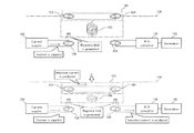
- FIG. 1 illustrates a switch device 100 as installed according to Embodiment 1.
- FIG. 2 is an overall schematic diagram of the switch device 100 pertaining to Embodiment 1.
- FIGS. 3A-3E illustrate the configuration of the switch device 100 pertaining to Embodiment 1.
- FIGS. 4A and 4B are schematic diagram of the operations of the switch device 100 pertaining to Embodiment 1.
- FIG. 5 is a flowchart of the operations of a determiner 140 pertaining to Embodiment 1.
- FIG. 6 shows an example of induced current occurring in a key bottom receiving coil 109 over time, pertaining to Embodiment 1.
- FIG. 7 is an overall schematic diagram of a switch device 200 pertaining to Embodiment 2.
- FIG. 8 shows an example of induced current occurring in a key bottom receiving coil over time, pertaining to Embodiment 2.
- FIG. 9 is an overall schematic diagram of a switch device 400 pertaining to Embodiment 3.
- FIG. 10 shows an example of induced current occurring in a key bottom receiving coil over time, pertaining to Embodiment 3.
- FIGS. 11A and 11B are overall schematic diagrams of a switch device pertaining to Patent Literature 1.
- FIG. 12 illustrates an implementation example of the switch device.
- a switch device having high durability is desired.
- a switch device In a typical switch device, physical contact between a switch key top and a switch key bottom is detected to perform a switch key top pressing detection. Such a switch device poses a problem in that insufficient contact may occur over the course of repeated use, as contact pins are subject to friction and waste adhesion.
- the switch device of Patent Literature 1 performs a pressing detection on a switch key top 601 , which is equipped with a coil A 602 , by having a detection circuit 605 detect a phase of induced current produced in a coil B 604 when the switch key top 601 is pressed.
- the switch device of Patent Literature 1 does not use the physical contact with the switch key top for detection, and thus prevents incomplete contact from occurring due to the aforementioned issues of contact pin friction and waste adhesion.
- the switch device of Patent Literature 1 uses wiring to connect the coil A 602 to a current production circuit 603 supplying electric current. As such, this wiring is worn down over the course of repeated pressing on the switch key top 601 , and may lead to problems in that pressing determination of the switch key top 601 is made inappropriately.
- the inventors have arrived at the switch device of the present disclosure, by discovering that the effect of induced current is usable for making the switch key top pressing detection, and does not require wiring imposing a load according to relative displacement of the switch key top and the switch key bottom.
- a switch device 100 pertaining to Embodiment 1 is, for example, installed on a mobile terminal 10 as shown in FIG. 1 .
- FIG. 2 is a schematic diagram of the switch device 100 .
- the switch device 100 includes a switch key top 101 and a switch key bottom 106 .
- the switch key top 101 is a flat, rectangular plate as large as a human index finger that includes a key top receiving coil 103 and a key top transmitting coil 104 . As shown in FIG. 2 , the two coils are provided with a degree of mutual separation.
- the switch key top 101 is, for example, made of a moulded insulating resin.
- the key top receiving coil 103 and the key top transmitting coil 104 are spiral coils. As shown in FIG. 3A , the spiral coils are formed by printing on a substrate 102 .
- the key top receiving coil 103 and the key top transmitting coil 104 are connected to each other by a connection pattern 111 .
- the switch key top 101 has a bottom face with an axial rod 105 protruding from the centre thereof.
- the axial rod 105 is inserted into a hole 115 of the later-described switch key bottom 106 so as to slide freely.
- the switch key bottom 106 is a switch base that is part of or is provided on the mobile terminal 10 , and has a concavity 107 in a top face thereof for accommodating the switch key top 101 .
- the concavity 107 has the hole 115 formed therein for passing the axial rod 105 of the switch key top 101 .
- the hole 115 has a coil spring 117 arranged therein.
- a key groove 115 a is formed vertically in a part of the circumferential wall of the hole 115 .
- a ball-shaped protrusion 105 a is formed on a circumferential wall of the axial rod 105 of the switch key top 101 , in correspondence with the key groove 115 a.
- the ball-shaped protrusion 105 a fits into the key groove 115 a when the switch key top 101 is pressed.
- the ball-shaped protrusion 105 a serves as a guide within the key groove 115 a and prevents the switch key top 101 from rotating irregularly.
- the ball-shaped protrusion 105 a has elastic bias applied thereto by the coil spring 117 under the axial rod 105 .
- the key groove 115 a is shaped to make the top of the hole 115 unreachable. That is, the key groove 115 a is not formed at the top of the hole 115 .
- the ball-shaped protrusion 105 a is set up to receive elastic bias so that, when the switch key top 101 and switch key bottom 106 are assembled, the ball-shaped protrusion 105 a retreats within the axial rod 105 to allow insertion into the hole 115 . However, after assembly, the ball-shaped protrusion 105 a protrudes into the key groove 115 a and prevents easy removal from the hole 115 .
- FIG. 3C illustrates the positional relationship of the switch key top 101 and the switch key bottom 106 when the switch key top 101 is not being pressed.
- FIG. 3D illustrates the positional relationship of the switch key top 101 and the switch key bottom 106 when the switch key top 101 is pressed to maximum depth.
- the bottom face of the concavity 107 in the switch key bottom 106 is provided with a key bottom transmitting coil 108 and a key bottom receiving coil 109 , respectively corresponding to the key top receiving coil 103 and the key top transmitting coil 104 of the switch key top 101 .
- the key bottom transmitting coil 108 is connected to a current supplier 120 of the switch key bottom 106 and the key bottom receiving coil 109 is connected to an A/D converter 130 of the switch key bottom 106 .
- the current supplier 120 uses a phase-locked loop (hereinafter, PLL) or the like to generate alternating current at a predetermined frequency, and supplies the alternating current to the key bottom transmitting coil 108 .
- PLL phase-locked loop
- the A/D converter 130 converts an induced current, induced in the key bottom receiving coil 109 by magnetic induction, into a digital value.
- a determiner 140 determines the state of the switch key top 101 by comparing the digital value obtained from the A/D converter 130 to threshold I and threshold II, serving as references for press determination.
- the current supplier 120 the A/D converter 130 , and the determiner 140 are provided on the switch key bottom 106 .
- these components may also be incorporated into a semiconductor integrated circuit within the mobile terminal 10 .
- FIGS. 4A and 4B are schematic diagrams of the operations of the switch device 100 .
- the current supplier 120 supplies current to the key bottom transmitting coil 108 , thereby producing a magnetic field in the key bottom transmitting coil 108 .
- the key top receiving coil 103 and the key bottom transmitting coil 104 are connected at this time, such that the force of induction causes current flow in the key top transmitting coil 104 .
- the magnetic field lines produced by the current are interlinked with the key bottom receiving coil 109 and produce an induced current therein. Current flow then reaches an input circuit of the A/D converter 130 , which outputs a digital value in accordance with an analogue value.
- the determiner 140 determines the state of the switch key top 101 by comparing the digital value obtained from the A/D converter 130 to threshold I and threshold II, serving as references for press determination.
- FIG. 5 is a flowchart describing the operations of the determiner 140 .
- the switch key top 101 is found not to be pressed (S 12 ).
- the switch key top 101 is found to be half pressed (S 14 ).
- the switch key top 101 is found to be fully pressed (S 15 ).
- FIG. 6 illustrates the induced current produced in the key bottom receiving coil 109 over time, in response to operation and non-operation of the switch key top 101 .
- the key bottom receiving coil 103 and the key bottom transmitting coil 104 must be separated to an extent sufficient for preventing cross-talk.
- the effect of cross-talk can be avoided by appropriately setting the thresholds used by the determiner 140 to compensate for a certain level of cross-talk.
- the current supplier 120 supplies periodically-varying current to the key bottom transmitting coil 108 .
- the flux interlinking the transmitting coil and the receiving coil in response to the current varies even when the switch is not pressed, and may produce a slight induced current. However, this slight amount is not enough to prevent determination of pressing by the determiner 140 .
- Embodiment 1 describes a switch device determining pressing in one place.
- the switch device may also be configured as a switch device determining pressing in a plurality of places, such as on a directional pad.
- Embodiment 2 discloses a switch device determining pressing in a plurality of places.
- FIG. 7 shows a switch device 200 pertaining to Embodiment 2.
- the switch device 200 includes a switch key top 201 and a switch key bottom 206 .
- the switch key top 201 is a directional pad having an X axis and a Y axis with ends A, B, C, and D. Each of the ends A, B, C, and D is configured identically to the switch key top of Embodiment 1. Coil patterns a 1 , b 1 , c 1 , and d 1 are provided, and connect the key top transmitting coil and key top receiving coil at each of the ends.
- the switch key bottom 206 is provided with a concavity 207 shaped to accommodate the switch key top 201 .
- coil springs 217 a , 217 b , 217 c , and 217 d are provided at predetermined positions of a bottom face of the concavity 207 in correspondence with the ends A, B, C, and D of the switch key top 201 .
- the coil springs 217 a , 217 b , 217 c , and 217 d keep the switch key top 201 elevated above the bottom face of the concavity 207 .
- a protrusion 208 is provided at the centre of the concavity 20 , and is shaped as a cone.
- the protrusion 208 is in contact with the switch key top 201 such that when one of the ends A, B, C, or D of the switch key top 201 is pressed, the other ends are prevented from also being driven downward. Furthermore, the protrusion 209 is not required in cases where the ability to press all of the ends A, B, C, and D simultaneously to turn all switches ON is desired.
- the bottom face of the concavity 207 of the switch key bottom 206 has key bottom transmitting coils a 2 , b 2 , c 2 , and d 2 and key bottom receiving coils a 3 , b 3 , c 3 , and d 3 , provided in correspondence with the key top receiving coil and the key top transmitting coil of the ends A, B, C, and D of the switch key top 201 .
- the key bottom transmitting coils a 2 , b 2 , c 2 , and d 2 are connected to the current supplier as described in Embodiment 1, and the key bottom receiving coils a 3 , b 3 , c 3 , and d 3 are each separately connected to an A/D converter and a determiner as described in Embodiment 1.
- the above-described switch device 200 has four determiners, each independently determining whether a corresponding end A, B, C, or D of the switch key top 201 is pressed, according to induced current in the respective key bottom receiving coils a 3 , b 3 , c 3 , and d 3 .
- the operations of the switch device 200 pertaining to the pressing of the ends A, B, C, and D of the switch key top 201 are identical to the operations of the switch device 100 described in Embodiment 1 and the description thereof is thus omitted.
- FIG. 8 illustrates the induced current produced in the key bottom receiving coils a 3 , b 3 , c 3 , and d 3 over time, in response to the ends A, B, C, and D of the switch key top 201 being pressed.
- induced current in key bottom receiving coil a 3 has a digital value that is equal to or greater than threshold I. As such, a determination is made such that end A is being pressed. At the same time, the induced current in the other key bottom receiving coils b 3 , c 3 , and d 3 has a digital value less than threshold I. A determination is thus made that ends B, C, and D are not being pressed. Also, from t7 to t10, the induced current in key bottom receiving coils a 3 and d 3 has a digital value that is greater than or equal to threshold I. Thus, a determination is made that ends A and D are being pressed simultaneously.
- the switch key top is operated by pressing.
- the switch key top is operated by rotation. Rotation also causes a change in the distance between the switch key top coils and the switch key bottom coils, which produces an induced current and enables ON/OFF determination.
- the switch key top is simply rotated, which enables a special detection operation of detecting the rotation angle.
- FIG. 9 shows a switch device 400 pertaining to Embodiment 3.
- the switch device 200 includes a switch key top 401 and a switch key bottom 406 .
- the switch key top 401 has an axial rod 405 at the centre of a bottom face thereof.
- the axial rod 405 is inserted into an axial hole 415 so as to rotate freely.
- the axial hole 415 is formed in the centre of a bottom face of a concavity 407 in the switch key bottom 406 .
- the rotational configuration is identical to that of a conventional rotary switch. The details thereof are thus omitted.
- the switch key top 401 is configured identically to the switch key top of Embodiment, and has a pair of coil patterns respectively connected to a key top receiving coil s 1 and a key top transmitting coil s 2 , which are provided at positions offset from the centre.
- the switch key bottom 406 has key bottom transmitting coils a 4 , b 4 , c 4 , and d 4 and key bottom receiving coils a 5 , b 5 , c 5 , and d 5 arranged circumferentially at roughly 90-degree intervals and offset from the centre of the axial hole 415 so as to match the respective positions of the key top receiving coil s 1 and the key top transmitting coil s 2 .
- the positional relationship between the coils is identical to the position of the switch key top receiving coil s 1 and the switch key top transmitting coil s 2 .
- the key bottom transmitting coils a 4 , b 4 , c 4 , and d 4 are connected to the current supplier as described in Embodiment 2, and the key bottom receiving coils a 5 , b 5 , c 5 , and d 5 are separately connected to the A/D converter and to the determiner.
- the switch device 400 when the switch key top 401 is rotated, the key top receiving coil s 1 and the key top transmitting coil s 2 approach one of the pairs of key bottom transmitting coil and key bottom receiving coil on the switch key bottom. This approach intensifies magnetic linkage and produces an induced current. A determination of the rotation position reached by the switch key top 401 is made according to the induced current produced in one of the key bottom receiving coils.
- FIG. 10 illustrates the induced current produced in the key bottom receiving coils a 5 , b 5 , c 5 , and d 5 over time, in response to the switch key top 401 being rotated.
- key bottom receiving coil a 5 has an induced current that is greater than or equal to threshold I. Then, from t4 to t7, key bottom receiving coil d 5 has an induced current that is greater than or equal to threshold I, and from t8 to t11, key bottom receiving coil c 5 has an induced current that is greater than or equal to threshold I. Accordingly, a determination is made that from t0 to t11, the switch key top 401 is rotated rightward by 180 degrees.
- the switch device of the above-described Embodiments is described as including a A/D converter and a determiner that determines a relative change in operating state of a switch key top by using a current value of induced current produced in a key bottom receiving coil and digitized by the A/D converter.
- the A/D converter may be omitted, and the determiner may instead use the analogue value of the induced current in the key bottom receiving coil as-is to determine the relative change in operating state of the switch key top.
- the switch device of the above-described Embodiments has receiving coils and transmitting coils printed on a substrate. However, other coils such as windings or stacks may also be used. In recent years, coil miniaturization technology has become widespread.
- the current supplier may not supply current to the key bottom transmitting coil when, for example, the terminal on which the switch device is installed is in sleep mode or locked mode. Accordingly, the supply of current is constrained according to the current mode of the terminal on which the switch device is installed, which reduces electric power consumption for the terminal.
- the current supplier uses a PLL, for example. However, no limitation to the PLL is intended. Various other types of current-producing circuits may also be used.
- the current supplied to the key bottom transmitting coil need not necessarily be a high-speed signal having a fixed period like PLL, but may also be any signal with a period that is equal to or less than half the determination interval.
- an individual determination is made regarding whether each the ends A, B, C, and D of the switch key top 201 is pressed. However, no such limitation is intended. The determiner may also make a general determination of whether the switch key top 201 is being pressed.
- a determination may be made such that end A has been pressed toward end C, on the switch key top 201 .
- the switch device 200 is described as a directional pad. However, no such limitation is intended.
- the switch key top may have any of a variety of shapes. Furthermore, a determination may be made regarding pressing of the switch key top at any position.
- a single threshold I is used to make the pressing determination for each end A, B, C, and D of the switch key top 201 .
- the switch device 200 of Embodiment 2 may, like the switch device 100 of Embodiment 1, also use a plurality of thresholds to determine a plurality of pressing states according to the degree of pressing at each of the ends A, B, C, and D.
- the switch key top and the switch key bottom are described as being used with a rotation operation with respect to a relative displacement.
- the switch key top may also be configured for a sliding operation and a determination may be made regarding whether or not the switch key top has been slid.
- the switch key bottom may have a key bottom transmitting and receiving coil arranged over a slide operation line and determine the position of the key top transmitting coil according to induced current occurring in a key bottom receiving coil, thereby determining whether a slide operation is performed on the switch key top.
- the paired transmitting and receiving coils are provided as one pair on the switch key top and as four pairs on the switch key bottom. However, depending on the relative displacement operation performed on the switch key top and the switch key bottom, the paired transmitting and receiving coils may be provided in plurality on the switch key top while only one pair is provided on the switch key bottom.
- a single switch key top is provided.
- a plurality of switch key tops may be provided and a determination of relative displacement may be performed for each of the switch key tops.
- the relative displacement for each of the switch key tops need not be determined individually, but may be a general determination of switch operation made from a combination of current values in the switch key tops.
- the switch device of the above-described Embodiments may be used as a shutter button 700 - 1 of a still camera, as a record or zoom button ( 700 - 2 , 700 - 3 ) of a video camera, and so on.
- a switch device comprises: a switch key top and a switch key bottom that are freely displaceable relative to each other, wherein the switch key top includes a key top receiving coil and a key top transmitting coil that are connected to each other, and the switch key bottom includes: a key bottom transmitting coil having a relative positional relationship with the key top receiving coil that changes according to a relative displacement operation with respect to the switch key top; a key bottom receiving coil having a relative positional relationship with the key top transmitting coil that changes according to the relative displacement operation with respect to the switch key top; a current supplier supplying current to the key bottom transmitting coil; and a determiner determining a relative displacement with respect to the switch key top, according to an induced current occurring in the key bottom receiving coil.
- the switch device of aspect (A) uses the effect of induced current to determine the operating state of the switch key top, without requiring any wiring that would impose a load according to the relative displacement of the switch key top and the switch key bottom.
- the switch device of aspect (A) presents a great increase in durability, and can easily be installed in a water-resistance terminal.
- the switch key bottom further includes an A/D converter digitizing a current value of the induced current, and the determiner compares the current value of the induced current digitized by the A/D converter to a threshold serving as a basis for determination to determine the relative displacement with respect to the switch key top.
- the switch device of aspect (B) is able to correctly determine the operating state of the switch key top.
- the relative displacement operation is one of a pressing operation, a rotation operation, and a sliding operation.
- the threshold includes a first threshold value and a second threshold value that is larger than the first threshold value, and the determiner compares the current value to the first threshold value and to the second threshold value, and determines the relative displacement with respect to the switch key top according to an amount of pressing in the pressing operation.
- the switch device of aspect (D) is able to determine a plurality of pressing states according to an amount of pressing on the switch key top.
- the current supplier supplies the current to the key bottom transmitting coil when a terminal incorporating the switch device is in a standby state, and does not supply the current to the key bottom transmitting coil otherwise.
- the current supplier controls the supply of electricity according to a mode of the terminal, thereby achieving power consumption reduction.
- the key bottom transmitting coil is provided in plurality, each of the key bottom transmitting coils having an individual relative positional relationship with the key top receiving coil that changes according to the relative displacement operation with respect to the switch key top
- the key bottom receiving coil is provided in plurality, each of the key bottom receiving coils having an individual relative positional relationship with the key top transmitting coil that changes according to the relative displacement operation with respect to the switch key top
- the current supplier supplies the current to each of the key bottom transmitting coils
- the determiner determines the relative displacement with respect to the switch key top according to the induced current occurring each of the key bottom receiving coils.
- the switch device of aspect (F) is able to determine more operating states.
- the key bottom transmitting coil is provided in plurality, each of the key bottom transmitting coils having an individual relative positional relationship with the key top receiving coil that changes according to the relative displacement operation with respect to the switch key top
- the key bottom receiving coil is provided in plurality, each of the key bottom receiving coils having an individual relative positional relationship with the key top transmitting coil that changes according to the relative displacement operation with respect to the switch key top
- the current supplier supplies the current to each of the key bottom transmitting coils
- the A/D converter digitizes a respective current value of the induced current in each of the key bottom receiving coils
- the determiner compares the respective current value of the induced current in each of the key bottom receiving coils, digitized by the A/D converter, to the threshold serving as the basis for determination to determine the relative displacement with respect to the switch key top.
- the switch device of aspect (G) is able to correctly determine more operating states.
- the relative displacement operation is a pressing operation
- the key top receiving coil and the key top transmitting coil in the switch key top are connected to each other so as to be displaced by the pressing operation, in the switch key bottom, the relative positional relationship between the key bottom transmitting coil and the key top receiving coil changes according to the pressing operation, and the relative positional relationship between the key bottom receiving coil and the key top transmitting coil changes according to the pressing operation
- the current supplier supplies the current to the key bottom transmitting coil
- the determiner determines the relative displacement with respect to the switch key top according to the induced current occurring in the key bottom receiving coil due to the pressing operation.
- the switch device of aspect (H) is able to determine a pressing state at various pressing positions of the switch key top, such as on a directional pad. Also, the switch device of aspect (H) is able to determine an overall pressing state of the switch key top by using a combination of key bottom receiving coils producing induced current, such as when the switch key top is pressed obliquely.
- the key top receiving coil and the key top transmitting coil in the switch key top are connected to each other so as to be displaced by the pressing operation, in the switch key bottom, the key bottom transmitting coil is provided in plurality, each of the key bottom transmitting coils having an individual relative positional relationship with the key top receiving coil that changes according to the relative displacement operation with respect to the switch key top, the key bottom receiving coil is provided in plurality, each of the key bottom receiving coils having an individual relative positional relationship with the key top transmitting coil that changes according to the relative displacement operation with respect to the switch key top, the current supplier supplies the current to each of the key bottom transmitting coils, the A/D converter digitizes the respective current value of the induced current in each of the key bottom receiving coils, and the determiner compares each of the respective current values digitized by the A/D converter to the first threshold value and to the second threshold value to determine the relative displacement with respect to the switch key top.
- the switch device of aspect (I) is able to determine a pressing state according to the amount of pressing at various pressing positions of the switch key top, such as on a directional pad. Also, the switch device of aspect ( 1 ) is able to determine an overall pressing state of the switch key top by using a combination of key bottom receiving coils producing induced current, such as when the switch key top is pressed obliquely. Further, the switch device of aspect ( 1 ) is also able to determine the overall pressing state of the switch key top using a combination of induced current values produced in each of the key bottom receiving coils.
- the switch key top is provided in plurality, and the determiner determines the relative displacement with respect to each of the switch key tops.
- the switch device of aspect (J) not only determined individual operating states of each of a plurality of switch key tops, but also makes an overall determination for a plurality of a operating states of the switch device using a combination of key bottom receiving coils producing induction voltage, a combination of induced current values produced in each of the key bottom receiving coils, or both.
- the electronic terminal of aspect (K) is able to greatly improve switch durability.
- the switch device of the present disclosure enables a great increase in durability by determining a pressing state of a switch key top using the effect of electromagnetic induction without requiring wiring that imposes a load according to the relative displacement between a switch key top and a switch key bottom.
- the switch device is applicable to terminals with high switch usage requiring high durability therefor.
Landscapes
- Engineering & Computer Science (AREA)
- Power Engineering (AREA)
- Physics & Mathematics (AREA)
- General Physics & Mathematics (AREA)
- Theoretical Computer Science (AREA)
- Push-Button Switches (AREA)
- Switches That Are Operated By Magnetic Or Electric Fields (AREA)
Abstract
Description
[2] The switch device of the above-described Embodiments has receiving coils and transmitting coils printed on a substrate. However, other coils such as windings or stacks may also be used. In recent years, coil miniaturization technology has become widespread. For instance, stacked ceramic coils made using ferrite and microcoil windings are undergoing development. These may, of course, be applied to the present disclosure.
[3] In the switch device of the above-described Embodiments, the current supplier may not supply current to the key bottom transmitting coil when, for example, the terminal on which the switch device is installed is in sleep mode or locked mode. Accordingly, the supply of current is constrained according to the current mode of the terminal on which the switch device is installed, which reduces electric power consumption for the terminal.
[4] In the switch device of the above-described Embodiments, the current supplier uses a PLL, for example. However, no limitation to the PLL is intended. Various other types of current-producing circuits may also be used. The current supplied to the key bottom transmitting coil need not necessarily be a high-speed signal having a fixed period like PLL, but may also be any signal with a period that is equal to or less than half the determination interval.
[5] In the
[6] In Embodiment 2, described above, the
[7] In Embodiment 2, described above, a single threshold I is used to make the pressing determination for each end A, B, C, and D of the switch
[8] In the
[9] In the
[10] In the above-described Embodiments, a single switch key top is provided. However, no such limitation is intended. A plurality of switch key tops may be provided and a determination of relative displacement may be performed for each of the switch key tops. Furthermore, the relative displacement for each of the switch key tops need not be determined individually, but may be a general determination of switch operation made from a combination of current values in the switch key tops.
[11] The switch device of the above-described Embodiments may be installed in a variety of electronic terminals. For example, the switch device of the above-described Embodiments may be used as a home button in a smartphone or tablet terminal. Also, as shown in the example of
- 10 Mobile terminal
- 100, 200, 400 Switch device
- 101, 201, 401 Switch key top
- 102 Substrate
- 103 Key top receiving coil
- 104 Key top transmitting coil
- 105 Axial rod
- 105 a, 208 Protrusion
- 106, 206, 406 Switch key bottom
- 107, 207, 407 Concavity
- 108 Key bottom transmitting coil
- 109 Key bottom receiving coil
- 111 Connection pattern
- 115, 415 Hole
- 115 a Key groove
- 117, 217 Coil spring
- 120 Current supplier
- 130 A/D converter
- 140 Determiner
- 601 Switch key top
- 602 Coil A
- 603 Current production circuit
- 604 Coil B
- 605 Detection circuit
- 700-1, 700-2, 700-3 Switch device
- a1, b1, c1, d1 Coil pattern
- a2, b2, c2, d2, a4, b4, c4, d4 Key bottom transmitting coil
- a3, b3, c3, d3, a5, b5, c5, d5 Key bottom receiving coil
- s1 Key bottom transmitting coil
- s2 Key bottom receiving coil
Claims (9)
Applications Claiming Priority (3)
| Application Number | Priority Date | Filing Date | Title |
|---|---|---|---|
| JP2012-255239 | 2012-11-21 | ||
| JP2012255239 | 2012-11-21 | ||
| PCT/JP2013/006489 WO2014080578A1 (en) | 2012-11-21 | 2013-11-01 | Non-contact switch device |
Publications (2)
| Publication Number | Publication Date |
|---|---|
| US20140354070A1 US20140354070A1 (en) | 2014-12-04 |
| US9716496B2 true US9716496B2 (en) | 2017-07-25 |
Family
ID=50775775
Family Applications (1)
| Application Number | Title | Priority Date | Filing Date |
|---|---|---|---|
| US14/371,267 Expired - Fee Related US9716496B2 (en) | 2012-11-21 | 2013-11-01 | Non-contact switch device |
Country Status (5)
| Country | Link |
|---|---|
| US (1) | US9716496B2 (en) |
| JP (1) | JPWO2014080578A1 (en) |
| CN (1) | CN104067365B (en) |
| TW (1) | TWI608510B (en) |
| WO (1) | WO2014080578A1 (en) |
Families Citing this family (4)
| Publication number | Priority date | Publication date | Assignee | Title |
|---|---|---|---|---|
| US10675532B2 (en) | 2014-04-21 | 2020-06-09 | Steelseries Aps | Variable actuators of an accessory and methods thereof |
| US10022622B2 (en) | 2014-04-21 | 2018-07-17 | Steelseries Aps | Programmable actuation inputs of an accessory and methods thereof |
| WO2017179803A1 (en) * | 2016-04-15 | 2017-10-19 | Lg Electronics Inc. | Displacement sensor and camera module having the same |
| CN114125091B (en) * | 2020-08-31 | 2023-10-27 | 深圳市万普拉斯科技有限公司 | An input structure and electronic device |
Citations (9)
| Publication number | Priority date | Publication date | Assignee | Title |
|---|---|---|---|---|
| US4425511A (en) * | 1981-02-09 | 1984-01-10 | Amnon Brosh | Planar coil apparatus employing a stationary and a movable board |
| JPH0575012A (en) | 1991-09-18 | 1993-03-26 | Seiko Epson Corp | Semiconductor integrated circuit |
| JP2000311541A (en) | 1999-04-28 | 2000-11-07 | Nec Home Electronics Ltd | Key switch device |
| JP2001325066A (en) | 2000-05-15 | 2001-11-22 | Tokai Rika Co Ltd | Touch operation input device |
| JP2004087250A (en) | 2002-08-26 | 2004-03-18 | Paloma Ind Ltd | Noncontact switch device |
| JP2005100917A (en) | 2003-06-23 | 2005-04-14 | Casio Comput Co Ltd | Signal generation device, operation signal generation device, operation input device, camera release device, and electronic camera |
| JP2009245723A (en) | 2008-03-31 | 2009-10-22 | Brother Ind Ltd | Multidirectional key switch |
| JP2010192410A (en) | 2009-02-20 | 2010-09-02 | Nikon Corp | Button type switch, imaging device, and electronic device |
| JP2012049950A (en) | 2010-08-30 | 2012-03-08 | Tokai Rika Co Ltd | Combination switch |
Family Cites Families (3)
| Publication number | Priority date | Publication date | Assignee | Title |
|---|---|---|---|---|
| JPH0575012U (en) * | 1992-03-13 | 1993-10-12 | ナイルス部品株式会社 | Vehicle load control device |
| DE19840620C1 (en) * | 1998-09-05 | 2000-04-27 | Steute Schaltgeraete Gmbh & Co | Non-contact safety switch |
| JP2008026217A (en) * | 2006-07-24 | 2008-02-07 | Toshiba Corp | Proximity sensor and electronic device |
-
2013
- 2013-11-01 WO PCT/JP2013/006489 patent/WO2014080578A1/en not_active Ceased
- 2013-11-01 US US14/371,267 patent/US9716496B2/en not_active Expired - Fee Related
- 2013-11-01 JP JP2014548438A patent/JPWO2014080578A1/en active Pending
- 2013-11-01 CN CN201380006137.1A patent/CN104067365B/en not_active Expired - Fee Related
- 2013-11-18 TW TW102141916A patent/TWI608510B/en not_active IP Right Cessation
Patent Citations (9)
| Publication number | Priority date | Publication date | Assignee | Title |
|---|---|---|---|---|
| US4425511A (en) * | 1981-02-09 | 1984-01-10 | Amnon Brosh | Planar coil apparatus employing a stationary and a movable board |
| JPH0575012A (en) | 1991-09-18 | 1993-03-26 | Seiko Epson Corp | Semiconductor integrated circuit |
| JP2000311541A (en) | 1999-04-28 | 2000-11-07 | Nec Home Electronics Ltd | Key switch device |
| JP2001325066A (en) | 2000-05-15 | 2001-11-22 | Tokai Rika Co Ltd | Touch operation input device |
| JP2004087250A (en) | 2002-08-26 | 2004-03-18 | Paloma Ind Ltd | Noncontact switch device |
| JP2005100917A (en) | 2003-06-23 | 2005-04-14 | Casio Comput Co Ltd | Signal generation device, operation signal generation device, operation input device, camera release device, and electronic camera |
| JP2009245723A (en) | 2008-03-31 | 2009-10-22 | Brother Ind Ltd | Multidirectional key switch |
| JP2010192410A (en) | 2009-02-20 | 2010-09-02 | Nikon Corp | Button type switch, imaging device, and electronic device |
| JP2012049950A (en) | 2010-08-30 | 2012-03-08 | Tokai Rika Co Ltd | Combination switch |
Non-Patent Citations (1)
| Title |
|---|
| International Search Report issued Feb. 4, 2014 in International (PCT) Application No. PCT/JP2013/006489. |
Also Published As
| Publication number | Publication date |
|---|---|
| US20140354070A1 (en) | 2014-12-04 |
| WO2014080578A1 (en) | 2014-05-30 |
| TWI608510B (en) | 2017-12-11 |
| CN104067365A (en) | 2014-09-24 |
| CN104067365B (en) | 2017-03-01 |
| TW201421519A (en) | 2014-06-01 |
| JPWO2014080578A1 (en) | 2017-01-05 |
Similar Documents
| Publication | Publication Date | Title |
|---|---|---|
| US10033231B2 (en) | System and method for providing wireless power transfer functionality to an electrical device | |
| US20230298810A1 (en) | Receiver unit of a wireless power transfer system | |
| US9716496B2 (en) | Non-contact switch device | |
| US8712324B2 (en) | Inductive signal transfer system for computing devices | |
| CN204069546U (en) | There is the portable set containment vessel of slide connector | |
| WO2013093922A2 (en) | System and method for providing wireless power transfer functionality to an electrical device | |
| CN105934863B (en) | Power receiving device, power receiving control method, wireless power supply system, and electronic device | |
| US10615629B2 (en) | Wireless device | |
| TWI728652B (en) | Wireless charging mouse and charging method thereof | |
| US9985674B2 (en) | SIM card connector and mobile terminal having the SIM card connector | |
| JP2012205366A (en) | Input/output circuit | |
| CN105474507A (en) | Apparatus and method for non-compliant object detection | |
| US9985394B2 (en) | Polarity control for a flat connector | |
| JP2012139033A (en) | Non-contact power transmission system and power reception antenna | |
| EP3128623B1 (en) | Sim card connector | |
| CN111060851B (en) | Electronic equipment and card holder forward and backward insertion detection method | |
| US12261525B2 (en) | Power supply device, power supply system and method for controlling the same | |
| TW201803249A (en) | Wireless charging | |
| US20130076986A1 (en) | Batteryless digital television receiver | |
| US20170163091A1 (en) | Wireless power transmitter | |
| CN102842458A (en) | Magnetic control switch | |
| Kim et al. | An effective technique for preventing cross-connection errors in dense loosely-coupled wireless charging pad environments | |
| TWM421659U (en) | Digital television receiver with no battery | |
| KR100985908B1 (en) | Electrical connection system | |
| TW201312469A (en) | Radio frequency identifier structure of radio frequency identification (RFID) system |
Legal Events
| Date | Code | Title | Description |
|---|---|---|---|
| AS | Assignment |
Owner name: PANASONIC CORPORATION, JAPAN Free format text: ASSIGNMENT OF ASSIGNORS INTEREST;ASSIGNORS:WATANABE, KAZUHIRO;ISHINO, KOUICHI;NAKAYAMA, TAKESHI;AND OTHERS;SIGNING DATES FROM 20140612 TO 20140618;REEL/FRAME:034076/0614 |
|
| AS | Assignment |
Owner name: PANASONIC INTELLECTUAL PROPERTY MANAGEMENT CO., LT Free format text: ASSIGNMENT OF ASSIGNORS INTEREST;ASSIGNOR:PANASONIC CORPORATION;REEL/FRAME:034537/0136 Effective date: 20141110 |
|
| STCF | Information on status: patent grant |
Free format text: PATENTED CASE |
|
| FEPP | Fee payment procedure |
Free format text: MAINTENANCE FEE REMINDER MAILED (ORIGINAL EVENT CODE: REM.); ENTITY STATUS OF PATENT OWNER: LARGE ENTITY |
|
| LAPS | Lapse for failure to pay maintenance fees |
Free format text: PATENT EXPIRED FOR FAILURE TO PAY MAINTENANCE FEES (ORIGINAL EVENT CODE: EXP.); ENTITY STATUS OF PATENT OWNER: LARGE ENTITY |
|
| STCH | Information on status: patent discontinuation |
Free format text: PATENT EXPIRED DUE TO NONPAYMENT OF MAINTENANCE FEES UNDER 37 CFR 1.362 |
|
| FP | Lapsed due to failure to pay maintenance fee |
Effective date: 20210725 |